JP2004017171A - Electronic component and method of manufacturing the same - Google Patents
Electronic component and method of manufacturing the same Download PDFInfo
- Publication number
- JP2004017171A JP2004017171A JP2002171852A JP2002171852A JP2004017171A JP 2004017171 A JP2004017171 A JP 2004017171A JP 2002171852 A JP2002171852 A JP 2002171852A JP 2002171852 A JP2002171852 A JP 2002171852A JP 2004017171 A JP2004017171 A JP 2004017171A
- Authority
- JP
- Japan
- Prior art keywords
- substrate
- electronic component
- lid
- hole
- forming
- Prior art date
- Legal status (The legal status is an assumption and is not a legal conclusion. Google has not performed a legal analysis and makes no representation as to the accuracy of the status listed.)
- Pending
Links
Images


Landscapes
- Measuring Fluid Pressure (AREA)
- Photometry And Measurement Of Optical Pulse Characteristics (AREA)
- Micromachines (AREA)
- Piezo-Electric Or Mechanical Vibrators, Or Delay Or Filter Circuits (AREA)
Abstract
Description
【0001】
【発明の属する技術分野】
本発明は、封止体によって封止された電子部品、特に赤外線センサ、加速度センサ、圧力センサ、圧電共振子等の電子部品に関する。
【0002】
【従来の技術】
本発明の従来の技術として、特開平8−139339号公報に開示される技術がある。図12に断面図を示す。単結晶シリコンからなり、上面にエッチングなどにより形成された凹部25を有する素子形成基板20と、素子形成基板20上に形成された誘電体膜21と、前記凹部25上にあって、前記基板20に振動可能に支持されている、単結晶シリコンからなる振動部本体27、下部電極22a、圧電体膜23、上部電極22bがあり、単結晶シリコンからなり裏面に凹部12を有する蓋11によって振動部本体27が封止されている。蓋11にはコンタクトホール17が形成されており、コンタクトホール17を通して外部回路と上部電極22bおよび下部電極22aとの電気的接続をはかる。
【0003】
【発明が解決しようとする課題】
前記従来技術では、封止体である蓋11と素子形成基板20の接合部分にコンタクトホール17が設けられており、封止が難しいコンタクトホール17部分での封止が必要で、製造コストが上昇する。また、外部回路との接続は、コンタクトホール17を通して下部電極22aおよび上部電極22bと直接行うため、フリップチップ実装ができない。さらに、電極一箇所につき一つのコンタクトホール17をあける必要があるため、加工するコンタクトホール17の数が多くなって製造コストが上昇し、また、部品の小型化にも限界がある。
【0004】
本発明は、蓋材の側面に外部電極を形成することにより、前記従来技術よりも封止が容易で封止の信頼性も向上し、さらに、部品の小型化および部品のフリップチップ実装も可能となる電子部品を提供することを目的とする。
【0005】
【課題を解決するための手段】
上記の問題点を解決するために本発明は、素子部と蓋とからなる電子部品であって、前記素子部は素子形成基板を有し、前記蓋の側面には切り欠き部があり、前記切り欠き部では前記素子形成基板の上面が露出しており、前記切り欠き部と前記素子形成基板の上面が露出している部分とに外部電極が形成されていることを特徴とする。蓋の側面に切り欠き部を設けて素子形成基板の上面を露出させ、切り欠き部と素子形成基板の上面の露出している部分とに外部電極を形成することにより、素子部の電極と外部電極とが面と面とで接合して接合面が大きくなり、接合強度が大きくなる。
【0006】
前記外部電極が、前記蓋の側面と上面に形成されていることが好ましい。外部との電気的接続が容易であり、フリップチップ実装も可能となるからである。
【0007】
前記蓋と前記素子部とを接合する接合部材が、前記外部電極よりも内側に構成されていることが好ましい。孔によって外部電極を構成した場合、孔部分での封止は難しいからである。
【0008】
前記素子部が少なくとも1層以上の圧電体膜を有する薄膜部の上面と下面を少なくとも一対の上部電極および下部電極を対向させて挟む構造の振動部を有することが望ましい。このような振動部を有する電子部品は、振動部を封止することが必要であり、本発明の構造によれば低コストかつ信頼性の高い封止と電子部品の小型化を実現できるからである。
【0009】
前記素子形成基板に孔または凹部が設けられており、前記振動部が前記孔または前記凹部上に位置して前記素子形成基板に振動可能に支持されて形成されていることが望ましい。このようなダイヤフラム構造を有する電子部品に本発明は有効である。
【0010】
本発明において、素子部が圧電共振子あるいは赤外線センサであることが望ましい。圧電共振子あるいは赤外線センサは素子部の封止が必要であり、本発明によれば、低コストかつ信頼性の高い封止と電子部品の小型化を実現できるからである。
【0011】
前記素子部は、裏面基板を備えることが好ましい。該裏面基板によって、前記素子形成基板に形成された素子部の封止をするとともに、素子形成基板を補強する効果が得られる。
【0012】
前記蓋の裏面に凹部が形成されていることをが望ましい。凹部が、前記振動部の振動を許すための振動空間となるからである。
【0013】
前記接合部材の厚みが、前記振動部の厚みよりも厚いことが望ましい。接合部材の厚みによって形成される前記蓋と前記素子形成基板との間の空間が、前記振動部の振動を許すための振動空間となるからである。
【0014】
本発明の製造方法は、複数の蓋を一体に形成する蓋材基板に孔を形成する工程と、前記蓋材基板と素子形成基板を接合して積層体を形成する工程と、前記素子部の電極と電気的に接続する外部電極を前記孔に形成する工程と、複数個分の電子部品が一体に形成された前記積層体を前記孔上を通る線で切断して個々の電子部品を切り出す工程と、を含むことを特徴とする。複数個分の電子部品が一体に形成された前記積層体を前記孔上を通る線で切断して個々の電子部品を切り出すことにより、一つの孔が複数個の電子部品の外部電極となるから、加工する孔の数を減らすことができ、加工時間の短縮化によりコストダウンを図ることができる。また、個々の電子部品に占める孔の面積が小さくなるため、部品の小型化を図ることができる。あるいは、従来よりも口径の大きな孔を用いることも可能であり、サンドブラスト処理によって孔を形成するときには孔の口径が大きくなるほど加工速度が速くなるため、電子部品の加工時間が短縮されて加工コストが低減される。
【0015】
前記孔に導電材を充填してビアホールとし、前記ビアホールを外部電極とする工程を含むことが好ましい。
【0016】
前記蓋材基板と前記素子形成基板を接合する工程において、前記蓋材基板と前記素子形成基板を接合する接合部材を前記孔よりも内側に形成することが好ましい。孔より内側で封止を行うことになるので、技術的に難しい孔部分での封止を避けることができる。
【0017】
前記素子形成基板に裏面基板を接合する工程を含むことが好ましい。該裏面基板によって、前記素子形成基板に形成された素子部の封止をするとともに、素子形成基板を補強する効果が得られる。
【0018】
以上のような構成および製造方法により、封止が容易で封止の信頼性も高く、従来よりも小型の電子部品を提供することができる。
【0019】
【発明の実施の形態】
本発明の実施形態を、図面を用いて以下に説明する。本実施例では、圧電薄膜共振子を例に挙げて説明する。
【0020】
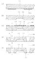
図1は、本発明の実施例における電子部品として、圧電薄膜共振子を示す断面図であり、図2は蓋材基板の工程を示す断面図であり、図3は蓋材基板の平面図を示す。パイレックスガラス(登録商標)などからなる蓋材基板10の裏面に、図2(a)に示すようにレジスト15aを形成し、このレジスト15aをマスクとして蓋材基板10にエッチングなどの方法によって図2(b)に示すように凹部12を形成する。凹部12は、素子部に形成される振動部の振動を許すための振動空間となる。次に、蓋材基板10の表面に図2(c)に示すようにレジスト15bを形成し、サンドブラスト処理などの方法より孔13を、図2(d)および図3に示すように切断線40をまたぐように形成する。この孔13が蓋の側面に形成される切り欠き部となり、切り欠き部に外部電極が形成されるので、一つの孔13が複数個分の圧電薄膜共振子の外部電極となるから、加工する孔13の数を減らすことができ、加工時間の短縮によって製造コストが低減される。また、個々の圧電薄膜共振子に占める孔13の面積が小さくなることから、圧電薄膜共振子の微細化が可能となる。あるいは、孔13が複数個の電子部品に分割されることになるため、従来よりも口径の大きい孔を用いることも可能となり、サンドブラスト処理によって孔13を形成する場合には加工する孔13の口径が大きいほど加工速度が速くなるため、電子部品の加工時間が短縮されて加工コストが低減される。
【0021】
図4は素子部の工程を示す断面図である。素子部は、素子形成基板20上に複数形成され、誘電体膜21、上部電極22b、下部電極22a、圧電体膜23からなる。まず、シリコンからなる素子形成基板20に、酸化シリコンの誘電体膜21を形成する。図4(a)は素子形成基板20と誘電体膜21を示す。次に、素子形成基板20の予め定められた範囲を素子形成基板20の裏面から誘電体膜21に至るまでエッチングし、ダイヤフラム24を形成する。図4(b)はダイヤフラム24が形成された状態を示している。図4(c)に示すように、誘電体膜21上に下部電極22a、酸化亜鉛などからなる圧電体膜23、上部電極22bを積層して振動部を形成する。下部電極22aおよび上部電極22bはアルミニウムなどの薄膜金属からなり、切断後には素子部の端部となる切断線40近くまで伸長して形成される。
【0022】
蓋材と素子部をそれぞれ形成した後、蓋材基板10と素子部が形成された素子形成基板20とを、例えばフリットガラスや接着剤などの接合部材14を用いて接合する。孔13が設けられている部分では、素子形成基板20の上面は露出している。また、図2(e)に示すように、蓋11と素子形成基板20とを接合する接合部材14は、孔13よりも内側に形成する。封止のための接合領域が孔13よりも内側に形成されることによって、ペーストなどの気密埋め込みや成膜による孔13部分での封止を行わずにすみ、封止が容易となり、また、封止の信頼性も向上する。図5(a)に素子形成基板と蓋材とを接合する前の状態を示す断面図を、図5(b)に蓋材基板と素子形成基板とを接合した後の状態を示す断面図をそれぞれ示す。また、図6は、蓋の裏面を示す斜視図である。接合部材14が、凹部12を取り囲んで形成されている状態を示す。蓋11は、蓋材基板10に複数個分を一体に形成し、素子部と接合した後にダイシングするが、図6では、蓋11一個分のみを図示している。孔13が蓋11の側面の切り欠き部となることがわかる。
【0023】
蓋材基板10と素子形成基板20を接合した後、孔13をすず半田などの導電材で充填してビアホールとし、素子部の上部電極22bおよび下部電極22aと電気的に接続する外部電極16を形成する。このとき、上部電極22bおよび下部電極22aは切断線40付近まで引き出されて形成されているため、上部電極22bあるいは下部電極22aと外部電極16との接合面が大きくなり、大きな接合強度が得られる。
【0024】
次に、振動部を裏面から封止するための裏面基板30を、素子形成基板20の裏面に接合する。裏面基板30は素子形成基板20の補強ともなる。図5(c)に孔13が導電材で充填され、裏面基板30が接合された状態の断面図を示す。蓋材基板10と素子形成基板20を形成する前、あるいは外部電極16を形成する前に裏面基板30を接合してもよい。
【0025】
本実施例においては、素子部が封止されてから外部電極16を形成するため、外部電極16の形成にあたってウェットプロセスを用いることが可能である。すなわち、例えばめっきやフォトリソグラフィーによって外部電極16を形成したり、ウェットエッチングによって外部電極16をパターニングすることなどができる。
【0026】
そして、ビアホール上を通っている切断線40をダイシングなどによって切断し、個々の圧電薄膜共振子を切り出す。圧電薄膜共振子が切り出された状態を図1に示す。ビアホールを外部電極16とし、ビアホール上を通る切断線でダイシングすることにより外部電極16は蓋11の側面より突出せずに形成され、外部電極16の位置および形状の精度が高く形成される。また、外部電極16は圧電薄膜共振子の表面にあり、蓋の側面と上面とに形成されているから、蓋11側が実装面となり、外部回路との接続は、ワイヤボンディングによる接続だけではなく、フリップチップ実装が可能である。
【0027】
以上、圧電薄膜共振子を例に挙げて実施の形態を説明してきたが、圧電薄膜共振子に限らず、封止を必要とする電子部品であればなんでもよく、例えば赤外線センサや加速度センサ、圧力センサ、デュプレクサなどであってもよい。
【0028】
上記実施例では、蓋材基板10にパイレックスガラス(登録商標)を用いているが、プラスチックやAl2O3セラミックス基板、シリコン基板などを用いてもよい。凹部12および孔13のいずれを先に形成するかは問わない。凹部12の形成方法は問わない。また、変形例として、図7に示したように、凹部12を形成せず、接合部材14の厚みによって振動部の振動を許す振動空間を確保する構造であってもよい。
【0029】
上記実施例では孔13はサンドブラスト処理によって形成しているが、CO2レーザやエッチングなどの方法によって形成してもよい。また、図3では、個々の電子部品に形成される外部電極の数が四個になっているが、電子部品の種類にあわせて孔13の数を変えることによって外部電極の数を変えることができる。例えば、図8に示すように孔13を形成すれば、個々の電子部品に設けられる外部電極の数は六個となる。
【0030】
素子部の上部電極22bおよび下部電極22aは、アルミニウムのほかにニッケル、金、白金、チタン、クロム、モリブデン、銅などの導電性金属であればよい。圧電体膜23は、酸化亜鉛やチタン酸ジルコン酸鉛、窒化アルミニウムなどの圧電性を有する材料であればよい。
【0031】
素子形成基板20にダイヤフラム24を形成する方法及びダイヤフラム24の形状は上記に限らず、例えば、図9に示すような工程であってもよい。図9(a)に示すように、素子形成基板20にエッチングなどの方法で凹部25を形成したのち、素子形成基板20の表面に誘電体膜21を形成する。次に、図9(b)に示すように、凹部を燐石英ガラスなどの下地材料26で埋める。そして、図9(c)に示すように下部電極22a、圧電体膜23および上部電極22bを積層して振動部を形成したのちにエッチングなどの方法で下地材料26を除去してダイヤフラム24を形成する。図9(d)は、ダイヤフラム24を形成した状態をしめす。そして、上記実施例に示した工程で作成した蓋材基板10や裏面基板30と接合し、外部電極16を形成したのちに切断線40で切断して個々の圧電薄膜共振子を切り出す。図10はこの方法で製造した圧電薄膜共振子の断面図である。この方法でダイヤフラム24を形成する場合、裏面基板30は接合されないこともある。
【0032】
裏面基板30は、素子形成基板20にダイヤフラム24を形成する工程の後であり、かつ個々の電子部品を切り出す工程の前であれば、どの工程の間でも素子形成基板20と接合してもよい。
【0033】
素子部が封止されてから外部電極16を形成するため、外部電極16の形成にあたってウェットプロセスを用いることが可能である。すなわち、例えばめっきやフォトリソグラフィーによって外部電極16を形成したり、ウェットエッチングによって外部電極16をパターニングすることなどができる。
【0034】
孔13を充填する導電材には、すず半田のほかに銀、銅などのペーストを用いることもできる。
【0035】
また変形例として、孔13をペーストで充填せずに、図11に示すようにスパッタや蒸着などの方法によって孔13の側面に金属膜を成膜して外部電極16とすることもできる。
【0036】
蓋材基板10と素子形成基板20を接合する前に、ペースト埋め込みや金属膜の成膜によって孔13に外部電極16を形成してもよい。この場合には、導電性接着剤によって外部電極16と上部電極22bおよび下部電極22aとの電気的接続を図る。
【0037】
【発明の効果】
以上のように本発明によれば、孔を複数の電子部品にまたがるように形成してあるから、一つの孔が複数個の電子部品の外部電極となり、加工する孔の数が少なくなって加工コストが低減される。また、電子部品に占める孔の面積が小さくなるから、電子部品のいっそうの小型化が可能となる。
【0038】
孔を導電材で埋めてビアホールとし、ビアホール上を通る先で切断するため、外部電極が電子部品の側面および上面に形成されているから、フリップチップ実装が可能である。
【0039】
また、蓋材と素子部の接合部分が孔よりも内側に設けられているため、孔部分での封止を行う必要がなく、封止が容易であり、封止の信頼性も向上する。
【0040】
また、本発明において素子部を赤外線センサあるいは圧電共振子とすることにより、小型かつ製造コストが低く、封止の信頼性も高い赤外線センサあるいは圧電共振子を得ることができる。
【0041】
裏面基板を接合することにより、振動部を封止するとともに、素子部の強度を増すことができる。
【0042】
本発明の製造方法によれば、複数の電子部品が一体に形成された後に個々の電子部品を切り出すから、複数の電子部品を一度に多数製造することができ、小型でかつ封止の信頼性の高い電子部品を低コストで製造できる。
【図面の簡単な説明】
【図1】本発明の実施例である圧電薄膜共振子を示す断面図である。
【図2】本発明の蓋材基板の工程を示す断面図である。
【図3】本発明の蓋材基板を示す平面図である。
【図4】本発明の素子部の工程を示す断面図である。
【図5】本発明の工程を示す断面図である。
【図6】本発明の蓋を示す斜視図である。
【図7】本発明の実施例の変形例を示す断面図である。
【図8】本発明の蓋材基板を示す平面図である。
【図9】本発明の素子部の工程を示す断面図である。
【図10】本発明の電子部品を示す断面図である。
【図11】本発明の実施例の変形例を示す断面図である。
【図12】従来の電子部品を示す断面図である。
【符号の説明】
10 蓋材基板
11 蓋
12 凹部
13 孔
14 接合部材
15a、15b レジスト
16 外部電極
17 コンタクトホール
20 素子形成基板
21 誘電体膜
22a 下部電極
22b 上部電極
23 圧電体膜
24 ダイヤフラム
25 凹部
26 下地材料
27 振動部本体[0001]
TECHNICAL FIELD OF THE INVENTION
The present invention relates to electronic components sealed by a sealing body, particularly to electronic components such as an infrared sensor, an acceleration sensor, a pressure sensor, and a piezoelectric resonator.
[0002]
[Prior art]
As a conventional technique of the present invention, there is a technique disclosed in JP-A-8-139339. FIG. 12 shows a sectional view. An
[0003]
[Problems to be solved by the invention]
In the above-described conventional technology, the
[0004]
The present invention forms an external electrode on the side surface of the lid member, so that the sealing is easier and the reliability of the sealing is improved as compared with the related art, and furthermore, the downsizing of the component and the flip chip mounting of the component are possible. It is intended to provide an electronic component that becomes
[0005]
[Means for Solving the Problems]
In order to solve the above problems, the present invention is an electronic component comprising an element portion and a lid, wherein the element portion has an element forming substrate, a side surface of the lid has a cutout portion, An upper surface of the element forming substrate is exposed in the notch, and an external electrode is formed in the notch and a portion where the upper surface of the element forming substrate is exposed. A notch is provided on the side surface of the lid to expose the upper surface of the element forming substrate, and external electrodes are formed on the notch and the exposed portion of the upper surface of the element forming substrate. The electrodes are joined face to face, so that the joining surface becomes large, and the joining strength increases.
[0006]
It is preferable that the external electrode is formed on a side surface and an upper surface of the lid. This is because electrical connection with the outside is easy and flip-chip mounting is also possible.
[0007]
It is preferable that a joining member that joins the lid and the element unit is formed inside the external electrode. This is because, when an external electrode is formed by holes, it is difficult to seal at the holes.
[0008]
It is preferable that the element section has a vibrating section having a structure in which the upper and lower surfaces of a thin film section having at least one or more piezoelectric films are sandwiched between at least a pair of upper and lower electrodes. The electronic component having such a vibrating portion needs to seal the vibrating portion, and according to the structure of the present invention, it is possible to realize low cost and highly reliable sealing and downsizing of the electronic component. is there.
[0009]
It is preferable that a hole or a concave portion is provided in the element forming substrate, and the vibrating portion is formed on the element forming substrate so as to be vibrated and positioned on the hole or the concave portion. The present invention is effective for an electronic component having such a diaphragm structure.
[0010]
In the present invention, it is desirable that the element portion is a piezoelectric resonator or an infrared sensor. This is because the piezoelectric resonator or the infrared sensor requires sealing of the element part, and according to the present invention, low-cost and highly reliable sealing and miniaturization of electronic components can be realized.
[0011]
Preferably, the element section includes a back substrate. The back substrate seals the element portion formed on the element forming substrate and has the effect of reinforcing the element forming substrate.
[0012]
It is preferable that a concave portion is formed on the back surface of the lid. This is because the concave portion becomes a vibration space for allowing the vibration of the vibrating portion.
[0013]
It is desirable that the thickness of the joining member is larger than the thickness of the vibrating part. This is because the space between the lid and the element forming substrate formed by the thickness of the joining member becomes a vibration space for allowing the vibration of the vibration portion.
[0014]
The manufacturing method of the present invention includes a step of forming a hole in a lid material substrate that integrally forms a plurality of lids, a step of joining the lid material substrate and an element forming substrate to form a laminate, Forming an external electrode electrically connected to an electrode in the hole, and cutting out the individual electronic components by cutting the laminate in which a plurality of electronic components are integrally formed by a line passing over the hole; And a step. By cutting the laminate in which a plurality of electronic components are integrally formed with a line passing over the holes and cutting out individual electronic components, one hole becomes an external electrode of the plurality of electronic components. The number of holes to be processed can be reduced, and the cost can be reduced by shortening the processing time. Further, since the area of the hole occupying each electronic component is reduced, the size of the component can be reduced. Alternatively, it is also possible to use a hole having a larger diameter than before, and when forming a hole by sandblasting, the processing speed increases as the hole diameter increases, so that the processing time of the electronic component is shortened and the processing cost is reduced. Reduced.
[0015]
The method preferably includes a step of filling the hole with a conductive material to form a via hole, and using the via hole as an external electrode.
[0016]
In the step of bonding the lid material substrate and the element formation substrate, it is preferable that a bonding member for bonding the lid material substrate and the element formation substrate is formed inside the hole. Since sealing is performed inside the hole, it is possible to avoid sealing at a hole portion that is technically difficult.
[0017]
It is preferable to include a step of bonding a back substrate to the element forming substrate. The back substrate seals the element portion formed on the element forming substrate and has the effect of reinforcing the element forming substrate.
[0018]
With the above-described configuration and manufacturing method, it is possible to provide an electronic component that is easily sealed, has high sealing reliability, and is smaller than a conventional electronic component.
[0019]
BEST MODE FOR CARRYING OUT THE INVENTION
An embodiment of the present invention will be described below with reference to the drawings. In this embodiment, a piezoelectric thin film resonator will be described as an example.
[0020]
FIG. 1 is a cross-sectional view showing a piezoelectric thin-film resonator as an electronic component according to an embodiment of the present invention, FIG. 2 is a cross-sectional view showing a process of a lid substrate, and FIG. 3 is a plan view of the lid substrate. Show. As shown in FIG. 2A, a resist 15a is formed on the back surface of the
[0021]
FIG. 4 is a cross-sectional view showing the steps of the element section. A plurality of element portions are formed on the
[0022]
After forming the lid member and the element portion, the
[0023]
After bonding the
[0024]
Next, a
[0025]
In this embodiment, since the
[0026]
Then, the cutting
[0027]
The embodiment has been described above by taking the piezoelectric thin-film resonator as an example. However, the present invention is not limited to the piezoelectric thin-film resonator, and may be any electronic component that requires sealing, such as an infrared sensor, an acceleration sensor, and a pressure sensor. It may be a sensor, a duplexer, or the like.
[0028]
In the above embodiment, Pyrex glass (registered trademark) is used for the
[0029]
In the above embodiment, the
[0030]
The upper electrode 22b and the lower electrode 22a of the element portion may be made of a conductive metal such as nickel, gold, platinum, titanium, chromium, molybdenum, and copper, in addition to aluminum. The
[0031]
The method for forming the
[0032]
The
[0033]
Since the
[0034]
As the conductive material filling the
[0035]
As a modified example, the
[0036]
The
[0037]
【The invention's effect】
As described above, according to the present invention, since a hole is formed so as to extend over a plurality of electronic components, one hole serves as an external electrode of a plurality of electronic components, and the number of holes to be processed is reduced, so that Cost is reduced. Further, since the area of the hole occupying the electronic component is reduced, the electronic component can be further reduced in size.
[0038]
Since the hole is filled with a conductive material to form a via hole and cut at a point passing over the via hole, flip-chip mounting is possible because external electrodes are formed on the side and top surfaces of the electronic component.
[0039]
Further, since the joining portion between the lid member and the element portion is provided inside the hole, there is no need to perform sealing at the hole portion, which facilitates sealing and improves sealing reliability.
[0040]
Further, by using an infrared sensor or a piezoelectric resonator as the element portion in the present invention, an infrared sensor or a piezoelectric resonator having a small size, low manufacturing cost, and high sealing reliability can be obtained.
[0041]
By joining the back substrate, the vibrating portion can be sealed and the strength of the element portion can be increased.
[0042]
According to the manufacturing method of the present invention, individual electronic components are cut out after a plurality of electronic components are integrally formed, so that a large number of electronic components can be manufactured at one time, and a small size and reliability of sealing are achieved. Electronic components with high cost can be manufactured at low cost.
[Brief description of the drawings]
FIG. 1 is a sectional view showing a piezoelectric thin-film resonator according to an embodiment of the present invention.
FIG. 2 is a cross-sectional view showing a step of a lid material substrate of the present invention.
FIG. 3 is a plan view showing a lid member substrate of the present invention.
FIG. 4 is a cross-sectional view showing a step of the element section of the present invention.
FIG. 5 is a sectional view showing a step of the present invention.
FIG. 6 is a perspective view showing a lid of the present invention.
FIG. 7 is a sectional view showing a modification of the embodiment of the present invention.
FIG. 8 is a plan view showing a lid substrate of the present invention.
FIG. 9 is a cross-sectional view showing a step of the element section of the present invention.
FIG. 10 is a sectional view showing an electronic component of the present invention.
FIG. 11 is a sectional view showing a modification of the embodiment of the present invention.
FIG. 12 is a sectional view showing a conventional electronic component.
[Explanation of symbols]
Claims (18)
前記素子部は少なくとも1層以上の圧電体膜を有する薄膜部の上面と下面を少なくとも一対の上部電極および下部電極を対向させて挟む構造の振動部を有し、前記素子形成基板に孔または凹部が設けられており、前記振動部が前記孔または前記凹部上に位置して前記素子形成基板に振動可能に支持されて形成されている圧電共振子あるいは赤外線センサであることを特徴とする電子部品。An electronic component comprising at least an element portion and a lid, wherein the element portion has an element formation substrate, and an external electrode is formed on at least a side surface of the lid and the element formation substrate. An electrode and the external electrode are electrically connected,
The element portion has a vibrating portion having a structure in which an upper surface and a lower surface of a thin film portion having at least one or more piezoelectric films are sandwiched with at least a pair of upper and lower electrodes opposed to each other. Wherein the vibrating portion is a piezoelectric resonator or an infrared sensor formed on the element forming substrate so as to be vibrated and positioned on the hole or the concave portion. .
前記蓋材基板と、複数の素子部が形成された素子形成基板とを接合して積層体を形成する工程と、
前記素子部の電極と電気的に接続する外部電極を前記孔に形成する工程と、
複数個分の電子部品が一体に形成された前記積層体を前記孔上を通る線で切断して個々の電子部品を切り出す工程と、
を含むことを特徴とする、電子部品の製造方法。Forming a hole in a lid material substrate integrally forming a plurality of lids,
A step of joining the lid material substrate and an element formation substrate on which a plurality of element portions are formed to form a laminate;
Forming an external electrode in the hole that is electrically connected to the electrode of the element portion;
A step of cutting out the individual electronic components by cutting the laminate in which a plurality of electronic components are integrally formed with a line passing over the hole,
A method for manufacturing an electronic component, comprising:
前記孔に外部電極を形成する工程と、
前記蓋材基板と、複数の素子部が形成された素子形成基板とを接合して積層体を形成する工程と、
複数個分の電子部品が一体に形成された前記積層体を前記孔上を通る線で切断して個々の電子部品を切り出す工程と、
を含むことを特徴とする、電子部品の製造方法。Forming a hole in a lid material substrate integrally forming a plurality of lids,
Forming an external electrode in the hole;
A step of joining the lid material substrate and an element formation substrate on which a plurality of element portions are formed to form a laminate;
A step of cutting out the individual electronic components by cutting the laminate in which a plurality of electronic components are integrally formed with a line passing over the hole,
A method for manufacturing an electronic component, comprising:
Priority Applications (1)
| Application Number | Priority Date | Filing Date | Title |
|---|---|---|---|
| JP2002171852A JP2004017171A (en) | 2002-06-12 | 2002-06-12 | Electronic component and method of manufacturing the same |
Applications Claiming Priority (1)
| Application Number | Priority Date | Filing Date | Title |
|---|---|---|---|
| JP2002171852A JP2004017171A (en) | 2002-06-12 | 2002-06-12 | Electronic component and method of manufacturing the same |
Publications (1)
| Publication Number | Publication Date |
|---|---|
| JP2004017171A true JP2004017171A (en) | 2004-01-22 |
Family
ID=31171603
Family Applications (1)
| Application Number | Title | Priority Date | Filing Date |
|---|---|---|---|
| JP2002171852A Pending JP2004017171A (en) | 2002-06-12 | 2002-06-12 | Electronic component and method of manufacturing the same |
Country Status (1)
| Country | Link |
|---|---|
| JP (1) | JP2004017171A (en) |
Cited By (18)
| Publication number | Priority date | Publication date | Assignee | Title |
|---|---|---|---|---|
| EP1585218A2 (en) * | 2004-04-06 | 2005-10-12 | Samsung Electronics Co., Ltd. | Bulk acoustic wave resonator and methods of making the same |
| JPWO2005062356A1 (en) * | 2003-12-24 | 2007-07-19 | 株式会社日立製作所 | Apparatus and manufacturing method thereof |
| JP2007522730A (en) * | 2004-02-05 | 2007-08-09 | エプコス アクチエンゲゼルシャフト | Electrical component and manufacturing method |
| US7436272B2 (en) | 2004-06-25 | 2008-10-14 | Murata Manufacturing Co., Ltd. | Piezoelectric device |
| US7443270B2 (en) | 2005-07-28 | 2008-10-28 | Kabushiki Kaisha Toshiba | Film bulk acoustic resonator, filter circuit and method for manufacturing a film bulk acoustic resonator |
| US7482194B2 (en) | 2004-03-31 | 2009-01-27 | Kabushiki Kaisha Toshiba | Electronic component having micro-electrical mechanical system |
| JP2009036627A (en) * | 2007-08-01 | 2009-02-19 | Denso Corp | Semiconductor device |
| JP2009068863A (en) * | 2007-09-10 | 2009-04-02 | Toshiba Corp | Infrared detecting element and infrared image sensor using it |
| US7663450B2 (en) | 2004-11-23 | 2010-02-16 | Samsung Electronics Co., Ltd. | Monolithic duplexer |
| JP2010535641A (en) * | 2007-08-07 | 2010-11-25 | クォルコム・メムズ・テクノロジーズ・インコーポレーテッド | MEMS device and wiring thereof |
| JP2011512260A (en) * | 2008-01-23 | 2011-04-21 | エプコス アクチエンゲゼルシャフト | MEMS component, method for manufacturing MEMS component, and method for handling MEMS component |
| CN102297741A (en) * | 2010-06-25 | 2011-12-28 | 中国科学院电子学研究所 | Silicon resonant air pressure sensor based on Micro-Electro-Mechanical Systems |
| JP2015039204A (en) * | 2014-09-29 | 2015-02-26 | 京セラ株式会社 | Elastic wave device and manufacturing method of the same |
| JP2017512307A (en) * | 2014-02-28 | 2017-05-18 | メジャメント スペシャリティーズ, インコーポレイテッド | Differential pressure detection die |
| JP2017112630A (en) * | 2017-02-06 | 2017-06-22 | 京セラ株式会社 | Acoustic wave device and method of manufacturing the same |
| JP2021503725A (en) * | 2018-10-31 | 2021-02-12 | ウーハン イエンシー マイクロ コンポーネンツ カンパニーリミテッド | Sound wave device and its manufacturing method |
| JP2021133478A (en) * | 2020-02-28 | 2021-09-13 | 京セラ株式会社 | Mems element and piezoelectric resonance device |
| JP2022508120A (en) * | 2018-12-29 | 2022-01-19 | 中芯集成電路(寧波)有限公司上海分公司 | Integrated structure of crystal resonator and control circuit and its integrated method |
-
2002
- 2002-06-12 JP JP2002171852A patent/JP2004017171A/en active Pending
Cited By (26)
| Publication number | Priority date | Publication date | Assignee | Title |
|---|---|---|---|---|
| JPWO2005062356A1 (en) * | 2003-12-24 | 2007-07-19 | 株式会社日立製作所 | Apparatus and manufacturing method thereof |
| JP4838732B2 (en) * | 2004-02-05 | 2011-12-14 | エプコス アクチエンゲゼルシャフト | Electrical component and manufacturing method |
| JP2007522730A (en) * | 2004-02-05 | 2007-08-09 | エプコス アクチエンゲゼルシャフト | Electrical component and manufacturing method |
| US7482194B2 (en) | 2004-03-31 | 2009-01-27 | Kabushiki Kaisha Toshiba | Electronic component having micro-electrical mechanical system |
| EP1585218A2 (en) * | 2004-04-06 | 2005-10-12 | Samsung Electronics Co., Ltd. | Bulk acoustic wave resonator and methods of making the same |
| US7622846B2 (en) | 2004-04-06 | 2009-11-24 | Samsung Electronics Co., Ltd. | Bulk acoustic wave resonator, filter and duplexer and methods of making same |
| EP1585218B1 (en) * | 2004-04-06 | 2012-04-04 | Samsung Electronics Co., Ltd. | Bulk acoustic wave resonator and methods of making the same |
| US7436272B2 (en) | 2004-06-25 | 2008-10-14 | Murata Manufacturing Co., Ltd. | Piezoelectric device |
| US8720023B2 (en) | 2004-11-23 | 2014-05-13 | Samsung Electronics Co., Ltd. | Method of manufacturing a monolithic duplexer |
| US7663450B2 (en) | 2004-11-23 | 2010-02-16 | Samsung Electronics Co., Ltd. | Monolithic duplexer |
| US7443270B2 (en) | 2005-07-28 | 2008-10-28 | Kabushiki Kaisha Toshiba | Film bulk acoustic resonator, filter circuit and method for manufacturing a film bulk acoustic resonator |
| JP2009036627A (en) * | 2007-08-01 | 2009-02-19 | Denso Corp | Semiconductor device |
| JP2010535641A (en) * | 2007-08-07 | 2010-11-25 | クォルコム・メムズ・テクノロジーズ・インコーポレーテッド | MEMS device and wiring thereof |
| JP2009068863A (en) * | 2007-09-10 | 2009-04-02 | Toshiba Corp | Infrared detecting element and infrared image sensor using it |
| US8674464B2 (en) | 2008-01-23 | 2014-03-18 | Epcos Ag | MEMS component, method for producing a MEMS component, and method for handling a MEMS component |
| JP2011512260A (en) * | 2008-01-23 | 2011-04-21 | エプコス アクチエンゲゼルシャフト | MEMS component, method for manufacturing MEMS component, and method for handling MEMS component |
| KR101561316B1 (en) * | 2008-01-23 | 2015-10-16 | 에프코스 아게 | Mems component, method for producing a mems component and method for handling a mems component |
| CN102297741A (en) * | 2010-06-25 | 2011-12-28 | 中国科学院电子学研究所 | Silicon resonant air pressure sensor based on Micro-Electro-Mechanical Systems |
| CN102297741B (en) * | 2010-06-25 | 2013-06-05 | 中国科学院电子学研究所 | Silicon resonant air pressure sensor based on Micro-Electro-Mechanical Systems |
| JP2017512307A (en) * | 2014-02-28 | 2017-05-18 | メジャメント スペシャリティーズ, インコーポレイテッド | Differential pressure detection die |
| JP2015039204A (en) * | 2014-09-29 | 2015-02-26 | 京セラ株式会社 | Elastic wave device and manufacturing method of the same |
| JP2017112630A (en) * | 2017-02-06 | 2017-06-22 | 京セラ株式会社 | Acoustic wave device and method of manufacturing the same |
| JP2021503725A (en) * | 2018-10-31 | 2021-02-12 | ウーハン イエンシー マイクロ コンポーネンツ カンパニーリミテッド | Sound wave device and its manufacturing method |
| US11362633B2 (en) | 2018-10-31 | 2022-06-14 | Wuhan Yanxi Micro Components Co., Ltd. | Acoustic wave device and fabrication method thereof |
| JP2022508120A (en) * | 2018-12-29 | 2022-01-19 | 中芯集成電路(寧波)有限公司上海分公司 | Integrated structure of crystal resonator and control circuit and its integrated method |
| JP2021133478A (en) * | 2020-02-28 | 2021-09-13 | 京セラ株式会社 | Mems element and piezoelectric resonance device |
Similar Documents
| Publication | Publication Date | Title |
|---|---|---|
| JP2004017171A (en) | Electronic component and method of manufacturing the same | |
| JP4588753B2 (en) | Electronic device package manufacturing method and electronic device package | |
| JP4212137B2 (en) | Bulk acoustic wave (BAW) filter having a top including a protective acoustic mirror | |
| JP4517992B2 (en) | Conducting hole forming method, piezoelectric device manufacturing method, and piezoelectric device | |
| US7564177B2 (en) | Crystal unit having stacked structure | |
| US7291904B2 (en) | Downsized package for electric wave device | |
| JP4221756B2 (en) | Piezoelectric oscillator and manufacturing method thereof | |
| WO2006106831A1 (en) | Surface acoustic wave device and method for manufacturing same | |
| KR20060069312A (en) | Surface acoustic wave device and manufacturing method thereof, ic card, and portable electronic device | |
| WO2010005061A1 (en) | Functional device and manufacturing method therefor | |
| JP2007005948A (en) | Electronic component and manufacturing method thereof | |
| JP4292825B2 (en) | Method for manufacturing quartz vibrating piece | |
| JP2008028713A (en) | Surface acoustic wave device | |
| JP4122512B2 (en) | Piezoelectric vibration device | |
| JP4706399B2 (en) | Oscillator and electronic equipment | |
| JP7161709B2 (en) | Electronic device and its manufacturing method | |
| JP6015010B2 (en) | Vibration element, vibrator, oscillator and electronic equipment | |
| WO2021059731A1 (en) | Piezoelectric vibration plate, piezoelectric vibration device, and method for manufacturing piezoelectric vibration device | |
| JP4535778B2 (en) | Device device manufacturing method | |
| JP2013046168A (en) | Manufacturing method of vibration device | |
| JP5599057B2 (en) | Package and piezoelectric vibrator | |
| WO2021210214A1 (en) | Piezoelectric vibrator and method for manufacturing same | |
| TW201234544A (en) | Sealing member for electronic component package, electronic component package, and method for manufacturing the sealing member for electronic component package | |
| JP4758123B2 (en) | Piezoelectric device and manufacturing method thereof | |
| JP2006157504A (en) | Piezoelectric device and method for manufacturing glass lid |
Legal Events
| Date | Code | Title | Description |
|---|---|---|---|
| A621 | Written request for application examination |
Free format text: JAPANESE INTERMEDIATE CODE: A621 Effective date: 20050510 |
|
| A977 | Report on retrieval |
Free format text: JAPANESE INTERMEDIATE CODE: A971007 Effective date: 20080428 |
|
| A131 | Notification of reasons for refusal |
Free format text: JAPANESE INTERMEDIATE CODE: A131 Effective date: 20080819 |
|
| A02 | Decision of refusal |
Free format text: JAPANESE INTERMEDIATE CODE: A02 Effective date: 20090113 |