【書類名】 明細書
【発明の名称】 多連チップ抵抗器の製造方法
【特許請求の範囲】
【請求項1】 分割溝を有するシート状基板の前記分割溝を跨いで前記シート状基板の上面および前記分割溝内にスパッタリング法により複数対の上面電極層を形成する工程と、前記複数対の上面電極層間を電気的に接続するように複数の抵抗層を形成する工程と、少なくとも前記複数の抵抗層を覆うように保護層を形成する工程と、前工程で得られた前記シート状基板の分割溝で前記シート状基板を短冊状基板に分割する工程と、前記短冊状基板を個片に分割する工程とを備えた多連チップ抵抗器の製造方法。
【請求項2】 分割溝を有するシート状基板の前記分割溝を跨いで前記シート状基板の上面および前記分割溝内にスパッタリング法により複数対の第1の上面電極層を形成する工程と、前記複数対の第1の上面電極層と電気的に接続するように複数対の第2の上面電極層を形成する工程と、前記複数対の第2の上面電極層間を電気的に接続するように複数の抵抗層を形成する工程と、少なくとも前記複数の抵抗層を覆うように保護層を形成する工程と、前工程で得られた前記シート状基板の分割溝で前記シート状基板を短冊状基板に分割する工程と、前記短冊状基板を個片に分割する工程とを備えた多連チップ抵抗器の製造方法。
【発明の詳細な説明】
【0001】
【発明の属する技術分野】
本発明は、各種電子機器に使用される多連チップ抵抗器の製造方法に関するものである。
【0002】
【従来の技術】
近年、電子機器の小型化に伴い、回路基板に使用される電子部品に対しても実装密度を上げるため、ますます小形化への要求が高まっている。抵抗器に対しても、実装基板上の実装面積を縮小化するため、小形な抵抗器だけでなく、独立抵抗素子が一つのユニットとなっている多連チップ抵抗器への要求が高まってきている。
【0003】
従来のこの種の抵抗器としては、実願平2−79430号(実開平4−3801号)のマイクロフィルムに開示されたものが知られている。
【0004】
以下、従来の多連チップ抵抗器およびその製造方法について、図面を参照しながら説明する。
【0005】
図9(a)は従来の多連チップ抵抗器の斜視図、図9(b)は同断面図である。
【0006】
図9(a),(b)において、1は両側面の中央に切欠き2を有するセラミックからなる基板である。3は基板1の上面の側部に設けられた二対の上面電極層である。4は二対の上面電極層3に一部が重なるように設けられた2つの抵抗層である。5は2つの抵抗層4を覆うように設けられた保護層である。6aは二対の上面電極層3に一部が重なるように基板1の側面から下面の側部にかけて設けられ、導電ペーストを印刷・焼成してなる二対の側面電極層である。6bは二対の上面電極層2および二対の側面電極層6aを覆うように設けられたはんだめっきまたはニッケルとはんだめっきからなるめっき層である。
【0007】
以上のように構成された従来の多連チップ抵抗器について、以下にその製造方法を説明する。
【0008】
図10(a),(b)および図11(a),(b)は従来の多連チップ抵抗器の製造方法を示す工程図である。
【0009】
まず、図10(a)に示すように、セラミックからなるシート状の基板8aにスルーホール9と、この基板8aを後工程で分割するための縦方向の分割溝10aおよび横方向の分割溝10bを形成する。
【0010】
次に、図10(b)に示すように、シート状の基板8aの上面に、複数対の上面電極層3を印刷形成し、さらに対となる上面電極層3の一部に重なるように複数の抵抗層4を印刷形成する。
【0011】
次に、図11(a)に示すように、複数の抵抗層3の全体を覆うように複数の保護層5を印刷形成した後、横方向の分割溝10b(図10(a),(b)に図示)に沿って分割し、短冊状の基板8bを得る。
【0012】
次に、図11(b)に示すように、短冊状の基板8bの上面電極層3に一部が重なるようにして短冊状の基板8bの側面から下面の側部にかけて側面電極層6aを塗着形成した後、短冊状の基板8bを縦方向の分割溝10aに沿って分割し、個片状の基板(図示せず)を得る。
【0013】
最後に、上面電極層3の一部および側面電極層6aの表面にはんだめっきまたはニッケルとはんだめっきを施すことにより、図9(a),(b)に示すようなめっき層6bを形成し、従来の多連チップ抵抗器を製造していた。
【0014】
【発明が解決しようとする課題】
しかしながら、上記従来の構成では、この多連チップ抵抗器をプリント基板等の実装基板にはんだ付けで実装した場合、図12(a)の実装状態を示す断面図に示すように、多連チップ抵抗器は側面電極層(図示せず)が設けられた側面と下面の側部との双方で実装基板のはんだランドパターン12にはんだ付けされ、このはんだによるフィレット13が形成された状態となる。この場合、図12(b)の実装状態の上面図に示すように、多連チップ抵抗器11の部品面積14に加えて側面をはんだ付けする面積15が必要であり、これらを合わせた実装面積16が必要となるものである。しかも、実装密度を向上させるため、部品外形寸法を小さくすればするほど、実装面積に対するはんだ付け面積の占める割合が大きくなり、その結果、電子機器を小型化するための実装密度を向上させることには限界が生ずるという課題を有していた。
【0015】
本発明は上記従来の課題を解決するもので、実装基板に実装した際の実装面積に占めるはんだ付け面積を低減できる多連チップ抵抗器の製造方法を提供することを目的とするものである。
【0016】
【課題を解決するための手段】
上記目的を達成するために本発明の多連チップ抵抗器の製造方法は、分割溝を有するシート状基板の前記分割溝を跨いで前記シート状基板の上面および前記分割溝内にスパッタリング法により複数対の上面電極層を形成する工程と、前記複数対の上面電極層間を電気的に接続するように複数の抵抗層を形成する工程と、少なくとも前記複数の抵抗層を覆うように保護層を形成する工程と、前工程で得られた前記シート状基板の分割溝で前記シート状基板を短冊状基板に分割する工程と、前記短冊状基板を個片に分割する工程とを備えたもので、この製造方法によれば、この製造方法により得られた多連チップ抵抗器をプリント基板等の実装基板に実装した際の実装面積に占めるはんだ付け面積を低減することができるものである。また、多連チップ抵抗器であるため、チップ抵抗器単品のものに比べて、はんだ付けによる実装時に必要なはんだランドパターンの面積をより小さくすることができるものである。
【0017】
【発明の実施の形態】
本発明の請求項1に記載の発明は、分割溝を有するシート状基板の前記分割溝を跨いで前記シート状基板の上面および前記分割溝内にスパッタリング法により複数対の上面電極層を形成する工程と、前記複数対の上面電極層間を電気的に接続するように複数の抵抗層を形成する工程と、少なくとも前記複数の抵抗層を覆うように保護層を形成する工程と、前工程で得られた前記シート状基板の分割溝で前記シート状基板を短冊状基板に分割する工程と、前記短冊状基板を個片に分割する工程とを備えたもので、この製造方法によれば、基板の側面全体ではなく、側面の一部のみに電極を形成するため、この多連チップ抵抗器を実装基板にはんだ付けで実装した際、はんだフィレットが形成される部分を小さくすることができ、これにより、実装面積に占めるはんだ付け面積を低減させることができるという作用を有するものである。
【0018】
本発明の請求項2に記載の発明は、分割溝を有するシート状基板の前記分割溝を跨いで前記シート状基板の上面および前記分割溝内にスパッタリング法により複数対の第1の上面電極層を形成する工程と、前記複数対の第1の上面電極層と電気的に接続されるように複数対の第2の上面電極層を形成する工程と、前記複数対の第2の上面電極層間を電気的に接続するように複数の抵抗層を形成する工程と、少なくとも前記複数の抵抗層を覆うように保護層を形成する工程と、前工程で得られた前記シート状基板の分割溝で前記シート状基板を短冊状基板に分割する工程と、前記短冊状基板を個片に分割する工程とを備えたもので、この製造方法によれば、基板の側面全体ではなく、側面の一部のみに電極を形成するため、この多連チップ抵抗器を実装基板にはんだ付けで実装した際、はんだフィレットが形成される部分を小さくすることができ、これにより、実装面積に占めるはんだ付け面積を低減させることができるという作用を有するものである。
【0019】
(実施の形態1)
以下、本発明の実施の形態1における多連チップ抵抗器およびその製造方法について、図面を参照しながら説明する。
【0020】
図1は本発明の実施の形態1における多連チップ抵抗器の断面図である。
【0021】
図1において、21は96%のアルミナを含有してなる絶縁性の基板である。22は基板21の上面の側部から側面の一部にかけて金系のスパッタリング法により設けられた金属材料からなる複数対の上面電極層であり、この上面電極層22の稜線には丸みをもたせている。また基板21の側面上に設けられた上面電極層22の面積は、基板21の側面の面積の半分以下である。23は前記複数対の上面電極層22に電気的に接続するように基板21の上面に設けられた酸化ルテニウムを主成分とする複数の抵抗層である。24は少なくとも前記複数の抵抗層23の上面を覆うように設けられたガラスまたは樹脂等からなる保護層である。25、26は必要に応じて上面電極層22を覆うように設けられ、かつはんだ付け時の信頼性等を確保できるようにしたニッケルめっき層およびはんだめっき層である。
【0022】
以上のように構成された本発明の実施の形態1における多連チップ抵抗器の製造方法について、以下に図面を参照しながら説明する。
【0023】
図2(a)〜(c)および図3(a)〜(c)は本発明の実施の形態1における多連チップ抵抗器の製造方法を示す工程図である。
【0024】
まず、図2(a)に示すように、表面に後工程で短冊状および個片状に分割するために設けた複数の縦方向および横方向の分割溝27、28を有する耐熱性および絶縁性に優れた96%のアルミナを含有してなるシート状基板21の上面全体および縦方向、横方向の分割溝27、28内にスパッタリング工法により金を着膜する。この後、フォトリソ法により、着膜された金を所望の電極パターンとして約300〜400℃の温度で熱処理を行い、複数対の上面電極層22を形成する。このとき横方向の分割溝28内まで金を着膜するため、横方向の分割溝28の奥まで上面電極層22を形成することができる。また、この縦方向および横方向の分割溝27、28のシート状基板21の厚みに対する深さは、製造工程での取り扱い時に割れないように、シート状基板21の厚みの半分以下になるように形成されている。
【0025】
次に、図2(b)に示すように、複数対の上面電極層22間を電気的に接続するようにシート状基板21の上面に酸化ルテニウムを主成分とする抵抗ペーストを印刷後、約850℃で焼成して複数の抵抗層23を形成する。
【0026】
次に、図2(c)に示すように、抵抗層23の抵抗値を所定の値に修正するために、YAGレーザーでトリミング溝29を施してトリミングを行う。このとき、抵抗値測定用のトリミングプローブは、上面電極層22上にセットしてトリミングを行う。
【0027】
次に、図3(a)に示すように、抵抗値修正済みの抵抗層23を保護するため、少なくとも抵抗層23を覆うようにガラスを主成分とするペーストを印刷し、約600℃で焼成して保護層24を形成する。この場合、横方向に並ぶ複数の抵抗層23を縦方向の分割溝27を跨いで連続して覆うように保護層24の印刷パターンを形成してもよい。
【0028】
次に、図3(b)に示すように、上面電極層22、抵抗層23、トリミング溝29、保護層24を形成したシート状基板21を横方向の分割溝28に沿って分割し、短冊状基板30を形成する。このとき、短冊状基板30の長手方向の側面には、先に形成した上面電極層22が横方向の分割溝28の深さまで形成された状態になっている。
【0029】
最後に、図3(c)に示すように、露出している上面電極層22にめっきを施すための準備工程として、短冊状基板30を縦方向の分割溝27に沿って分割し、個片状の基板31を形成する。そして露出している上面電極層22を覆うように電気めっきによって、ニッケルめっき層(図示せず)と、はんだめっき層(図示せず)とを形成して、多連チップ抵抗器を製造するものである。
【0030】
以上のように構成、かつ製造された本発明の実施の形態1における多連チップ抵抗器をプリント基板等の実装基板にはんだ付けで実装した状態について説明する。
【0031】
図4(a)は本発明の実施の形態1における多連チップ抵抗器の実装状態を示す断面図、図4(b)は同上面図である。本発明の実施の形態1における多連チップ抵抗器を保護層24を下にしてプリント基板等の実装基板のはんだランドパターン32にはんだ付けで実装した場合、図4(a)に示すように、基板21の側面に設けられた側面電極層(図示せず)の面積が小さいため、基板21の側面にはほとんどはんだが付かず、このはんだによるフィレット33がわずかに形成されるのみとなる。すなわち、基板21の側部に設けられた上面電極層(図示せず)で実装基板のはんだランドパターン32にはんだ付けされ、このはんだによるフィレット33がわずかに形成された状態となる。このとき、図4(b)の実装状態の上面図に示すように、多連チップ抵抗器の部品面積34に対して側面をはんだ付けする面積35は小さくなり、その結果、これらを合わせた実装面積36を低減させることができるものである。
【0032】
また、図4(b)のように、部品面積34と側面をはんだ付けするために必要な面積35とを合わせた面積が実装面積36となる場合、例えば1.0×1.0mmサイズの多連チップ抵抗器を実装して従来構造の製品と実装面積を比較すると、約20%の縮小化を図ることができるものである。よって、本発明の構成によれば、基板21の側面に設けられた電極の面積が小さいため、この多連チップ抵抗器をプリント基板等の実装基板に実装した際、実装面積に占めるはんだ付け面積を低減させることができるとともに、フィレット33を小さく形成するため、使用するはんだの量を低減させることができるものである。
【0033】
なお、本発明の実施の形態1において、はんだめっき層26と保護層24とを面一またははんだめっき層26の高さを保護層24より高くすることにより、はんだめっき層26と実装時のランドパターン32との隙間が生じにくく実装品質をさらに向上させることができるものである。
【0034】
また、本発明の実施の形態1において、複数対の上面電極層22、複数の抵抗層23および保護層24を(表1)に示す組み合わせとしたときには、(表1)に示すように、他の特性を向上させることができるものである。
【0035】
【表1】
【0036】
(実施の形態2)
以下、本発明の実施の形態2における多連チップ抵抗器およびその製造方法について、図面を参照しながら説明する。
【0037】
図5は本発明の実施の形態2における多連チップ抵抗器の断面図である。
【0038】
図5において、41は96%のアルミナを含有してなる絶縁性の基板である。42は基板41の上面の側部から側面の一部にかけて金系のスパッタリング法により設けられた金属材料からなる複数対の第1の上面電極層であり、この第1の上面電極層42の稜線には丸みをもたせている。また基板41の側面上に設けられた第1の上面電極層42の面積は、基板41の側面の面積の半分以下である。43は前記複数対の第1の上面電極層42に電気的に接続するように基板41の上面に設けられた銀系の導電粉体にガラスを含有してなる複数対の第2の上面電極層である。44は前記複数対の第2の上面電極層43に電気的に接続するように基板41の上面に設けられた酸化ルテニウムを主成分とする複数の抵抗層である。45は少なくとも複数の抵抗層44の上面を覆うように設けられたガラスまたは樹脂等からなる保護層である。46、47は必要に応じて第1、第2の上面電極層42、43を覆うように設けられ、かつはんだ付け時の信頼性等を確保できるようにしたニッケルめっき層およびはんだめっき層である。
【0039】
以上のように構成された本発明の実施の形態2における多連チップ抵抗器の製造方法について、以下に図面を参照しながら説明する。
【0040】
図6(a)〜(c)および図7(a)〜(d)は本発明の実施の形態2における多連チップ抵抗器の製造方法を示す工程図である。
【0041】
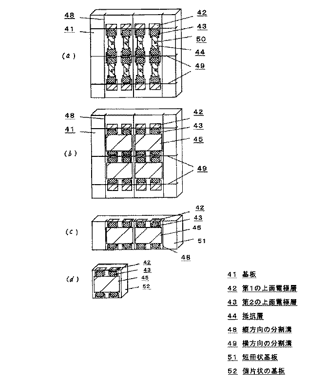
まず、図6(a)に示すように、表面に後工程で短冊状および個片状に分割するために設けた複数の縦方向および横方向の分割溝48、49を有する耐熱性および絶縁性に優れた96%のアルミナを含有してなるシート状基板41の上面全体および縦方向、横方向の分割溝48、49内にスパッタリング工法により金を着膜する。この後、フォトリソ法により、着膜された金を所望の電極パターンとして約300〜400℃の温度で熱処理を行い、複数対の第1の上面電極層42を形成する。このとき横方向の分割溝49内まで金を着膜するため、横方向の分割溝49の奥まで第1の上面電極層42を形成することができる。また、この縦方向および横方向の分割溝48、49のシート状基板41の厚みに対する深さは、製造工程での取り扱い時に割れないように、基板41の厚みの半分以下になるように形成されている。
【0042】
次に、図6(b)に示すように、複数対の第1の上面電極層42の一部に重なるようにシート状基板41の上面に銀系の導電粉体とガラスとを含有してなる電極ペーストを印刷後、約850℃で焼成して複数対の第2の上面電極層43を形成する。
【0043】
次に、図6(c)に示すように、複数対の第2の上面電極層43間を電気的に接続するようにシート状基板41の上面に酸化ルテニウムを主成分とする抵抗ペーストを印刷後、約850℃で焼成して複数の抵抗層44を形成する。
【0044】
次に、図7(a)に示すように、抵抗層44の抵抗値を所定の値に修正するために、YAGレーザーでトリミング溝50を施してトリミングを行う。このとき、抵抗値測定用のトリミングプローブは、第2の上面電極層43上にセットしてトリミングを行う。
【0045】
次に、図7(b)に示すように、抵抗値修正済みの抵抗層44を保護するため、少なくとも抵抗層44を覆うようにガラスを主成分とするペーストを印刷し、約600℃で焼成して保護層45を形成する。この場合、横方向に並ぶ複数の抵抗層44を縦方向の分割溝48を跨いで連続して覆うように保護層45の印刷パターンを形成してもよい。
【0046】
次に、図7(c)に示すように、第1の上面電極層42、抵抗層44、トリミング溝50、保護層45を形成したシート状基板41を横方向の分割溝49に沿って分割し、短冊状基板51を形成する。このとき、短冊状基板51の長手方向の側面には、先に形成した第1の上面電極層42が横方向の分割溝49の深さまで形成された状態になっている。
【0047】
最後に、図7(d)に示すように、露出している第1、第2の上面電極層42、43にめっきを施すための準備工程として、短冊状基板51を縦方向の分割溝48に沿って分割し、個片状の基板52を形成する。そして露出している第1、第2の上面電極層42、43を覆うように電気めっきによって、ニッケルめっき層(図示せず)と、はんだめっき層(図示せず)とを形成して、多連チップ抵抗器を製造するものである。
【0048】
以上のように構成、かつ製造された本発明の実施の形態2における多連チップ抵抗器をプリント基板等の実装基板にはんだ付けで実装した状態について説明する。
【0049】
図8(a)は本発明の実施の形態2における多連チップ抵抗器の実装状態を示す断面図、図8(b)は同上面図である。本発明の実施の形態2における多連チップ抵抗器を保護層45を下にしてプリント基板等の実装基板のはんだランドパターン53にはんだ付けで実装した場合、図8(a)に示すように、基板41の側面に設けられた側面電極層(図示せず)の面積が小さいため、基板41の側面にはほとんどはんだが付かず、このはんだによるフィレット54がわずかに形成されるのみとなる。すなわち、基板41の側部に設けられた第1、第2の上面電極層(図示せず)で実装基板のはんだランドパターン53にはんだ付けされるため、このはんだによるフィレット54がわずかに形成された状態となる。このとき、図8(b)の実装状態の上面図に示すように、多連チップ抵抗器の部品面積55に対して側面をはんだ付けする面積56は小さくなり、その結果、これらを合わせた実装面積57を低減させることができるものである。
【0050】
また、図8(b)のように、部品面積55と側面をはんだ付けするために必要な面積56とを合わせた面積が実装面積57となる場合、例えば1.0×1.0mmサイズの多連チップ抵抗器を実装して従来構造の製品と実装面積を比較すると、約20%の縮小化を図ることができるものである。よって、本発明の構成によれば、基板41の側面に設けられた電極の面積が小さいため、この多連チップ抵抗器をプリント基板等の実装基板に実装した際、実装面積に占めるはんだ付け面積を低減させることができるとともに、フィレット54を小さく形成できるため、使用するはんだの量を低減させることができるものである。
【0051】
なお、本発明の実施の形態2において、はんだめっき層47と保護層45とを面一またははんだめっき層47の高さを保護層45より高くすることにより、はんだめっき層47と実装時のランドパターン53との隙間が生じにくくなって、実装品質をさらに向上させることができるものである。
【0052】
また、本発明の実施の形態2において、複数対の上面電極層42、複数の第2の上面電極層43、複数の抵抗層44および保護層45を(表2)に示す組み合わせとしたときには、(表2)に示すように、他の特性を向上させることができるものである。
【0053】
【表2】
【0054】
【発明の効果】
以上のように本発明の多連チップ抵抗器の製造方法によれば、複数対の上面電極層が、基板の上面の側部から側面の一部にかけて設けられており、そして基板の側面に設けられている上面電極層は基板の厚みの半分以外であり、さらにこの上面電極層は、基板の側面全体ではなく、側面の一部のみに設けられているため、この多連チップ抵抗器を実装基板にはんだ付けで実装した際、はんだフィレットが形成される部分を小さくすることができ、これにより、実装面積に占めるはんだ付け面積を低減させることができるものである。また、多連チップ抵抗器であるため、チップ抵抗器単品のものに比べて、はんだフィレットを複数対形成する必要がなく、これにより、はんだ付けによる実装時に必要なはんだランドパターンの面積をより小さくすることができるため、さらに実装面積を低減させることができるという効果を奏するものである。
【図面の簡単な説明】
【図1】
本発明の実施の形態1における多連チップ抵抗器の断面図
【図2】
(a)〜(c)同多連チップ抵抗器の製造方法を示す工程図
【図3】
(a)〜(c)同多連チップ抵抗器の製造方法を示す工程図
【図4】
(a)同多連チップ抵抗器の実装状態を示す断面図
(b)同多連チップ抵抗器の実装状態を示す上面図
【図5】
本発明の実施の形態2における多連チップ抵抗器の断面図
【図6】
(a)〜(c)同多連チップ抵抗器の製造方法を示す工程図
【図7】
(a)〜(d)同多連チップ抵抗器の製造方法を示す工程図
【図8】
(a)同多連チップ抵抗器の実装状態を示す断面図
(b)同多連チップ抵抗器の実装状態を示す上面図
【図9】
(a)従来の多連チップ抵抗器の斜視図
(b)従来の多連チップ抵抗器の断面図
【図10】
(a)(b)同多連チップ抵抗器の製造方法を示す工程図
【図11】
(a)(b)同多連チップ抵抗器の製造方法を示す工程図
【図12】
(a)同多連チップ抵抗器の実装状態を示す断面図
(b)同多連チップ抵抗器の実装状態を示す上面図
【符号の説明】
21,41 基板
22 上面電極層
23,44 抵抗層
24,45 保護層
27,48 縦方向の分割溝
28,49 横方向の分割溝
30,51 短冊状基板
31,52 個片状の基板
42 第1の上面電極層
43 第2の上面電極層
[Document name] Specification [Title of invention] Manufacturing method of multiple chip resistor [Claims]
1. A step of forming a plurality of pairs of upper surface electrode layers on the upper surface of the sheet-shaped substrate and in the divided grooves by a sputtering method across the divided grooves of a sheet-shaped substrate having a dividing groove, and the plurality of pairs. A step of forming a plurality of resistance layers so as to electrically connect the upper surface electrode layers, a step of forming a protective layer so as to cover at least the plurality of resistance layers, and a step of forming the sheet-like substrate obtained in the previous step. A method for manufacturing a multiple chip resistor, comprising a step of dividing the sheet-shaped substrate into strip-shaped substrates by a dividing groove and a step of dividing the strip-shaped substrate into individual pieces.
2. A step of forming a plurality of pairs of first upper surface electrode layers on the upper surface of the sheet-shaped substrate and in the divided grooves by a sputtering method across the divided grooves of the sheet-shaped substrate having the divided grooves, and the above-mentioned step. The step of forming the plurality of pairs of the second upper surface electrode layers so as to electrically connect the plurality of pairs of the first upper surface electrode layers and the plurality of pairs of the second upper surface electrode layers so as to electrically connect the layers. The sheet-like substrate is formed into a strip-shaped substrate by a step of forming a plurality of resistance layers, a step of forming a protective layer so as to cover at least the plurality of resistance layers, and a dividing groove of the sheet-like substrate obtained in the previous step. A method for manufacturing a multiple chip resistor, comprising a step of dividing the strip-shaped substrate into individual pieces and a step of dividing the strip-shaped substrate into individual pieces.
Description: TECHNICAL FIELD [Detailed description of the invention]
[0001]
[Technical field to which the invention belongs]
The present invention relates to a method for manufacturing a multiple chip resistor used in various electronic devices.
0002.
[Conventional technology]
In recent years, with the miniaturization of electronic devices, there is an increasing demand for miniaturization in order to increase the mounting density of electronic components used for circuit boards. As for resistors, in order to reduce the mounting area on the mounting board, there is an increasing demand for not only small resistors but also multiple chip resistors in which independent resistance elements are one unit. There is.
0003
As a conventional resistor of this type, the one disclosed in the microfilm of Jitsugyo No. 2-79430 (Jitsukaihei No. 4-3801) is known.
0004
Hereinafter, a conventional multiple chip resistor and a method for manufacturing the same will be described with reference to the drawings.
0005
9 (a) is a perspective view of a conventional multiple chip resistor, and FIG. 9 (b) is a cross-sectional view of the conventional multiple chip resistor.
0006
FIG. 9 (a), in (b), 1 is a substrate made of ceramic with a cut-out 2 in the center of both sides. Reference numeral 3 denotes two pairs of upper surface electrode layers provided on the side surface of the upper surface of the substrate 1. Reference numeral 4 denotes two resistance layers provided so as to partially overlap the two pairs of upper surface electrode layers 3. Reference numeral 5 denotes a protective layer provided so as to cover the two resistance layers 4. Reference numeral 6a is two pairs of side electrode layers provided from the side surface of the substrate 1 to the side surface of the lower surface so as to partially overlap the two pairs of upper surface electrode layers 3, and the conductive paste is printed and fired. Reference numeral 6b is a solder plating or a plating layer composed of nickel and solder plating provided so as to cover the two pairs of the upper surface electrode layers 2 and the two pairs of the side electrode layers 6a.
0007
The manufacturing method of the conventional multiple chip resistor configured as described above will be described below.
0008
10 (a) and 10 (b) and 11 (a) and 11 (b) are process charts showing a method of manufacturing a conventional multiple chip resistor.
0009
First, as shown in FIG. 10 (a), a through hole 9 in a sheet-like substrate 8a made of ceramic, vertical dividing grooves 10a and lateral dividing groove 10b for dividing in a subsequent step the substrate 8a To form.
0010
Next, as shown in FIG. 10 (b), the upper surface of the sheet-like substrate 8a, a plurality to the top electrode layer 3 of the plurality of pairs formed by printing, overlaps a part of the upper surface electrode layers 3 becomes more pairs The resistance layer 4 of the above is printed and formed.
0011
Next, as shown in FIG. 11 (a), after printing and forming the plurality of protective layers 5 so as to cover the entire plurality of resistance layers 3, the lateral dividing grooves 10b (FIGS. 10 (a) and 10 (b)). ) Is divided to obtain a strip-shaped substrate 8b.
0012
Next, as shown in FIG. 11 (b), coating the side surface electrode layers 6a so as to partially overlap the upper surface electrode layers 3 of the strip-shaped substrate 8b from the side surface of the strip-shaped substrate 8b toward the lower surface side After forming, the strip-shaped substrate 8b is divided along the vertical dividing groove 10a to obtain an individual piece-shaped substrate (not shown).
0013
Finally, by applying solder plating or nickel and solder plating on the surface of the portion of the upper surface electrode layers 3 and the side electrode layers 6a, FIG. 9 (a), forming a plating layer 6b as (b), the A conventional multi-chip resistor was manufactured.
0014.
[Problems to be Solved by the Invention]
However, in the above-mentioned conventional configuration, when this multiple chip resistor is soldered to a mounting board such as a printed circuit board, the multiple chip resistor is shown in the cross-sectional view showing the mounting state of FIG. 12 (a). The vessel is soldered to the solder land pattern 12 of the mounting board on both the side surface provided with the side electrode layer (not shown) and the side portion of the lower surface, and the fillet 13 is formed by this solder. In this case, as shown in the top view of the mounting state of FIG. 12 (b), the requires area 15 for soldering the side surfaces in addition to the component area 14 of the array type chip resistor 11, mounting the total area of these 16 is required. Moreover, in order to improve the mounting density, the smaller the external dimensions of the parts, the larger the ratio of the soldered area to the mounting area, and as a result, the mounting density for miniaturizing electronic devices is improved. Had the problem of limitations.
0015.
The present invention solves the above-mentioned conventional problems, and an object of the present invention is to provide a method for manufacturing a multiple chip resistor capable of reducing the soldering area occupying the mounting area when mounted on a mounting board.
0016.
[Means for solving problems]
In order to achieve the above object, a plurality of methods for manufacturing a multiple chip resistor of the present invention are performed by a sputtering method on the upper surface of the sheet-shaped substrate and in the divided grooves across the divided grooves of the sheet-shaped substrate having the divided grooves. A step of forming a pair of top electrode layers, a step of forming a plurality of resistance layers so as to electrically connect the plurality of pairs of top electrode layers, and a step of forming a protective layer so as to cover at least the plurality of resistance layers. A step of dividing the sheet-shaped substrate into strip-shaped substrates by a dividing groove of the sheet-shaped substrate obtained in the previous step, and a step of dividing the strip-shaped substrate into individual pieces. According to this manufacturing method, it is possible to reduce the soldering area occupying the mounting area when the multiple chip resistor obtained by this manufacturing method is mounted on a mounting board such as a printed circuit board. Further, since it is a multiple chip resistor, the area of the solder land pattern required for mounting by soldering can be made smaller than that of a single chip resistor.
[0017]
BEST MODE FOR CARRYING OUT THE INVENTION
According to the first aspect of the present invention, a plurality of pairs of upper surface electrode layers are formed on the upper surface of the sheet-shaped substrate and in the divided grooves by a sputtering method so as to straddle the divided grooves of the sheet-shaped substrate having the divided grooves. A step, a step of forming a plurality of resistance layers so as to electrically connect the plurality of pairs of upper surface electrode layers, a step of forming a protective layer so as to cover at least the plurality of resistance layers, and a step obtained in the previous step. The sheet-shaped substrate is divided into strip-shaped substrates by the divided grooves of the sheet-shaped substrate, and the strip-shaped substrate is divided into individual pieces. According to this manufacturing method, the substrate is divided. Since the electrodes are formed only on a part of the side surface, not on the entire side surface, when this multiple chip resistor is soldered to the mounting board, the part where the solder fillet is formed can be reduced. Therefore, it has an effect that the soldering area occupying the mounting area can be reduced.
0018
The invention according to claim 2 of the present invention is a plurality of pairs of first upper surface electrode layers by a sputtering method in the upper surface of the sheet-shaped substrate and in the divided grooves straddling the divided grooves of the sheet-shaped substrate having the divided grooves. A step of forming a plurality of pairs of the second upper surface electrode layers so as to be electrically connected to the plurality of pairs of the first upper surface electrode layers, and a step of forming the plurality of pairs of the second upper surface electrode layers. In the step of forming a plurality of resistance layers so as to electrically connect the two, a step of forming a protective layer so as to cover at least the plurality of resistance layers, and a dividing groove of the sheet-like substrate obtained in the previous step. It includes a step of dividing the sheet-shaped substrate into strip-shaped substrates and a step of dividing the strip-shaped substrate into individual pieces. According to this manufacturing method, not the entire side surface of the substrate but a part of the side surface thereof. Since the electrodes are formed only on the mounting board, when this multiple chip resistor is mounted on the mounting board by soldering, the portion where the solder fillet is formed can be reduced, thereby reducing the soldering area occupying the mounting area. It has the effect of being able to reduce it.
0019
(Embodiment 1 )
Hereinafter, the multiple chip resistor according to the first embodiment of the present invention and a method for manufacturing the same will be described with reference to the drawings.
0020
FIG. 1 is a cross-sectional view of the multiple chip resistor according to the first embodiment of the present invention.
0021.
In FIG. 1 , reference numeral 21 denotes an insulating substrate containing 96% alumina. Reference numeral 22 denotes a plurality of pairs of upper surface electrode layers made of a metal material provided by a gold-based sputtering method from a side portion to a part of the upper surface surface of the substrate 21 , and the ridgeline of the upper surface electrode layer 22 is rounded. There is. The area of the upper surface electrode layers 22 provided on the side surface of the substrate 21 is less than half the area of the side surface of the substrate 21. Reference numeral 23 denotes a plurality of resistance layers containing ruthenium oxide as a main component, which are provided on the upper surface of the substrate 21 so as to be electrically connected to the plurality of pairs of upper surface electrode layers 22. Reference numeral 24 denotes a protective layer made of glass, resin or the like provided so as to cover at least the upper surfaces of the plurality of resistance layers 23. Reference numerals 25 and 26 are a nickel plating layer and a solder plating layer, which are provided so as to cover the upper surface electrode layer 22 as needed and can ensure reliability at the time of soldering.
0022.
The method for manufacturing the multiple chip resistor according to the first embodiment of the present invention configured as described above will be described below with reference to the drawings.
[0023]
2 (a) to 2 (c) and 3 (a) to 3 (c) are process diagrams showing a method for manufacturing a multiple chip resistor according to the first embodiment of the present invention.
0024
First, as shown in FIG. 2 (a), heat resistance and insulation have a plurality of vertical and horizontal dividing grooves 27 , 28 provided on the surface for dividing into strips and individual pieces in a later process. Gold is deposited on the entire upper surface of the sheet-shaped substrate 21 containing 96% alumina, and in the dividing grooves 27 and 28 in the vertical and horizontal directions by a sputtering method. Then, by the photolithography method, the film-formed gold is heat-treated at a temperature of about 300 to 400 ° C. as a desired electrode pattern to form a plurality of pairs of upper surface electrode layers 22. At this time, since the gold is applied to the inside of the dividing groove 28 in the lateral direction, the upper surface electrode layer 22 can be formed to the depth of the dividing groove 28 in the lateral direction. The depth to the thickness of the sheet-like substrate 21 of the vertical and horizontal dividing grooves 27, 28 so as not crack during handling in the manufacturing process, half to be less than the thickness of the sheet-like substrate 21 It is formed.
0025
Next, as shown in FIG. 2 (b), after printing a resistance paste containing ruthenium oxide as a main component on the upper surface of the sheet-shaped substrate 21 so as to electrically connect a plurality of pairs of the upper surface electrode layers 22, about A plurality of resistance layers 23 are formed by firing at 850 ° C.
0026
Next, as shown in FIG. 2 (c), to modify the resistance value of the resistive layer 23 to a predetermined value, trimming by performing trimming groove 29 in YAG laser. At this time, the trimming probe for measuring the resistance value is set on the upper surface electrode layer 22 for trimming.
[0027]
Next, as shown in FIG. 3 (a), in order to protect the resistance value corrected for the resistive layer 23, and printing a paste composed mainly of glass so as to cover at least the resistance layer 23, fired at about 600 ° C. To form the protective layer 24. In this case, the print pattern of the protective layer 24 may be formed so as to continuously cover the plurality of resistance layers 23 arranged in the horizontal direction across the division grooves 27 in the vertical direction.
[0028]
Next, as shown in FIG. 3 (b), the upper surface electrode layers 22, the resistance layer 23, the trimming groove 29 is divided along a sheet-like substrate 21 to form a protective layer 24 in the lateral direction of the dividing groove 28, the strip The shape substrate 30 is formed. At this time, the upper surface electrode layer 22 formed earlier is formed on the side surface of the strip-shaped substrate 30 in the longitudinal direction to the depth of the dividing groove 28 in the lateral direction.
[0029]
Finally, as shown in FIG. 3 (c), as a preparation step for plating the upper surface electrode layers 22 exposed, and divided along the strip-shaped substrate 30 in the longitudinal direction of the dividing grooves 27, pieces A shaped substrate 31 is formed. Then, a nickel plating layer (not shown) and a solder plating layer (not shown) are formed by electroplating so as to cover the exposed upper surface electrode layer 22, and a multiple chip resistor is manufactured. Is.
[0030]
A state in which the multiple chip resistor according to the first embodiment of the present invention, which is configured and manufactured as described above, is soldered to a mounting substrate such as a printed circuit board will be described.
0031
FIG. 4A is a cross-sectional view showing a mounted state of the multiple chip resistor according to the first embodiment of the present invention, and FIG. 4B is a top view of the same. When the multiple chip resistor according to the first embodiment of the present invention is soldered to the solder land pattern 32 of a mounting board such as a printed circuit board with the protective layer 24 facing down, as shown in FIG. 4A. Since the area of the side electrode layer (not shown) provided on the side surface of the substrate 21 is small, almost no solder is attached to the side surface of the substrate 21, and the fillet 33 formed by this solder is only slightly formed. That is, the upper surface electrode layer (not shown) provided on the side portion of the substrate 21 is soldered to the solder land pattern 32 of the mounting substrate, and the fillet 33 formed by this solder is slightly formed. At this time, as shown in the top view of the mounted state of FIG. 4 (b), the area 35 for soldering the side surface is smaller than the component area 34 of the multiple chip resistor, and as a result, these are combined and mounted. The area 36 can be reduced.
[0032]
Further, as shown in FIG. 4B, when the total area of the component area 34 and the area 35 required for soldering the side surface is the mounting area 36, for example, a large number of 1.0 × 1.0 mm size. Comparing the mounting area with a product having a conventional structure by mounting a continuous chip resistor, it is possible to reduce the size by about 20%. Therefore, according to the configuration of the present invention, since the area of the electrodes provided on the side surface of the substrate 21 is small, when this multiple chip resistor is mounted on a mounting board such as a printed circuit board, the soldering area occupying the mounting area. In addition to being able to reduce the amount of solder used, the amount of solder used can be reduced because the fillet 33 is formed to be small.
0033
In the first embodiment of the present invention, the solder plating layer 26 and the protective layer 24 are flush with each other, or the height of the solder plating layer 26 is made higher than that of the protective layer 24, so that the solder plating layer 26 and the land at the time of mounting are landed. It is possible to further improve the mounting quality because a gap with the pattern 32 is unlikely to occur.
0034
Further, in the first embodiment of the present invention, when the combination shown top electrode layer 22 of the plurality of pairs, a plurality of resistance layers 23 and a protective layer 24 in (Table 1), as shown in (Table 1), the other It is possible to improve the characteristics of.
0035.
[Table 1 ]
0036
(Embodiment 2 )
Hereinafter, the multiple chip resistor according to the second embodiment of the present invention and a method for manufacturing the same will be described with reference to the drawings.
0037
FIG. 5 is a cross-sectional view of the multiple chip resistor according to the second embodiment of the present invention.
[0038]
In FIG. 5 , reference numeral 41 denotes an insulating substrate containing 96% alumina. Reference numeral 42 denotes a plurality of pairs of first upper surface electrode layers made of a metal material provided by a gold-based sputtering method from a side portion to a part of the upper surface surface of the substrate 41 , and a ridge line of the first upper surface electrode layer 42. Is rounded. The area of the first upper surface electrode layer 42 provided on the side surface of the substrate 41 is less than half the area of the side surface of the substrate 41. Reference numeral 43 denotes a plurality of pairs of second upper surface electrodes formed by containing glass in a silver-based conductive powder provided on the upper surface of the substrate 41 so as to be electrically connected to the plurality of pairs of the first upper surface electrode layers 42. It is a layer. Reference numeral 44 denotes a plurality of resistance layers containing ruthenium oxide as a main component, which are provided on the upper surface of the substrate 41 so as to be electrically connected to the plurality of pairs of the second upper surface electrode layers 43. Reference numeral 45 denotes a protective layer made of glass, resin or the like provided so as to cover the upper surfaces of at least a plurality of resistance layers 44. Reference numerals 46 and 47 are nickel-plated layers and solder-plated layers that are provided so as to cover the first and second upper surface electrode layers 42 and 43 as needed and that can ensure reliability during soldering. ..
[0039]
The method for manufacturing the multiple chip resistor according to the second embodiment of the present invention configured as described above will be described below with reference to the drawings.
0040
6 (a) to 6 (c) and 7 (a) to 7 (d) are process diagrams showing a method for manufacturing a multiple chip resistor according to the second embodiment of the present invention.
[0041]
First, as shown in FIG. 6 (a), heat resistance and insulation have a plurality of vertical and horizontal dividing grooves 48 and 49 provided on the surface for dividing into strips and individual pieces in a later process. Gold is deposited on the entire upper surface of the sheet-shaped substrate 41 containing 96% alumina, and in the dividing grooves 48 and 49 in the vertical and horizontal directions by a sputtering method. Then, by the photolithography method, the film-formed gold is heat-treated at a temperature of about 300 to 400 ° C. as a desired electrode pattern to form a plurality of pairs of the first upper surface electrode layers 42. At this time, since the gold is applied to the inside of the dividing groove 49 in the lateral direction, the first upper surface electrode layer 42 can be formed to the depth of the dividing groove 49 in the lateral direction. Further, the depth of the vertical and horizontal dividing grooves 48 and 49 with respect to the thickness of the sheet-shaped substrate 41 is formed so as to be less than half the thickness of the substrate 41 so as not to be cracked during handling in the manufacturing process. ing.
[0042]
Next, as shown in FIG. 6 (b), contains a conductive powder and glass silver based on the upper surface of the sheet substrate 41 so as to overlap a portion of the first top electrode layer 42 of the plurality of pairs After printing, the electrode paste is fired at about 850 ° C. to form a plurality of pairs of second top electrode layers 43 .
[0043]
Next, as shown in FIG. 6 (c), a resistance paste containing ruthenium oxide as a main component is printed on the upper surface of the sheet-like substrate 41 so as to electrically connect a plurality of pairs of the second upper surface electrode layers 43. After that, it is fired at about 850 ° C. to form a plurality of resistance layers 44.
[0044]
Next, as shown in FIG. 7 (a), in order to modify the resistance value of the resistive layer 44 to a predetermined value, trimming by performing trimming groove 50 in YAG laser. At this time, the trimming probe for measuring the resistance value is set on the second upper surface electrode layer 43 to perform trimming.
0045
Next, as shown in FIG. 7 (b), for protecting the resistance value corrected for the resistive layer 44, and printing a paste composed mainly of glass so as to cover at least the resistance layer 44, fired at about 600 ° C. To form the protective layer 45. In this case, the print pattern of the protective layer 45 may be formed so as to continuously cover the plurality of resistance layers 44 arranged in the horizontal direction across the division grooves 48 in the vertical direction.
[0046]
Next, as shown in FIG. 7 (c), divided along the first upper surface electrode layers 42, the resistance layer 44, the trimming groove 50, the sheet-like substrate 41 to form a protective layer 45 in the lateral direction of the dividing grooves 49 Then, the strip-shaped substrate 51 is formed. At this time, the first upper surface electrode layer 42 formed earlier is formed on the side surface of the strip-shaped substrate 51 in the longitudinal direction to the depth of the division groove 49 in the lateral direction.
[0047]
Finally, as shown in FIG. 7 (d), first exposed, as a preparation step for plating the second upper surface electrode layers 42, 43, a strip-shaped substrate 51 in the longitudinal dividing grooves 48 It is divided along the above to form an individual piece-shaped substrate 52 . Then, a nickel plating layer (not shown) and a solder plating layer (not shown) are formed by electroplating so as to cover the exposed first and second upper surface electrode layers 42 and 43. It manufactures continuous chip resistors.
0048
A state in which the multiple chip resistor according to the second embodiment of the present invention, which is configured and manufactured as described above, is soldered to a mounting substrate such as a printed circuit board will be described.
[0049]
FIG. 8A is a cross-sectional view showing a mounted state of the multiple chip resistor according to the second embodiment of the present invention, and FIG. 8B is a top view of the same. When the multiple chip resistor according to the second embodiment of the present invention is soldered to the solder land pattern 53 of a mounting board such as a printed circuit board with the protective layer 45 facing down, as shown in FIG. 8 (a). Since the area of the side electrode layer (not shown) provided on the side surface of the substrate 41 is small, almost no solder is attached to the side surface of the substrate 41, and the fillet 54 formed by this solder is only slightly formed. That is, since the first and second upper surface electrode layers (not shown) provided on the side portion of the substrate 41 are soldered to the solder land pattern 53 of the mounting substrate, a fillet 54 formed by this solder is slightly formed. It will be in a state of being soldered. At this time, as shown in the top view of the mounted state of FIG. 8B, the area 56 for soldering the side surface is smaller than the component area 55 of the multiple chip resistor, and as a result, these are combined and mounted. The area 57 can be reduced.
0050
Further, as shown in FIG. 8B, when the total area of the component area 55 and the area 56 required for soldering the side surface is the mounting area 57, for example, a large number of 1.0 × 1.0 mm size. Comparing the mounting area with a product having a conventional structure by mounting a continuous chip resistor, it is possible to reduce the size by about 20%. Therefore, according to the configuration of the present invention, since the area of the electrodes provided on the side surface of the substrate 41 is small, when this multiple chip resistor is mounted on a mounting board such as a printed circuit board, the soldering area occupying the mounting area. The amount of solder used can be reduced because the fillet 54 can be formed to be small.
0051
In the second embodiment of the present invention, the solder plating layer 47 and the protective layer 45 are flush with each other, or the height of the solder plating layer 47 is made higher than that of the protective layer 45, so that the solder plating layer 47 and the land at the time of mounting are landed. The gap with the pattern 53 is less likely to occur, and the mounting quality can be further improved.
[0052]
In the second embodiment of the present invention, when the combination shown top electrode layer 42 of the plurality of pairs, the plurality of second upper surface electrode layers 43, a plurality of resistive layers 44 and the protective layer 45 (Table 2) As shown in (Table 2 ), other characteristics can be improved.
[0053]
[Table 2 ]
0054
【Effect of the invention】
According to the manufacturing method of multiple-chip resistor of the present invention as described above, the upper surface electrode layer pairs are provided over the portion of the side surface from the side of the upper surface of the substrate, and provided on the side surface of the substrate is in the upper surface electrode layers are is other than half the thickness of the substrate, further the upper electrode layer, not the entire side surface of the substrate, because it is provided only on a part of the side surface, mounting the multiple-chip resistor When the solder fillet is formed on the substrate by soldering, the portion where the solder fillet is formed can be reduced, whereby the soldering area occupying the mounting area can be reduced. Moreover, since a multiple-chip resistor, as compared with the chip resistor separately, it is not necessary to a plurality of pairs form a solder fillet, thereby more reducing the area of the soldering land pattern required when mounting by soldering Therefore, the mounting area can be further reduced.
[Simple explanation of drawings]
FIG. 1
FIG. 2 is a cross-sectional view of the multiple chip resistor according to the first embodiment of the present invention.
(A) to (c) FIG. 3 is a process diagram showing a method for manufacturing the same multiple chip resistor.
(A) to (c) FIG. 4 is a process diagram showing a method for manufacturing the same multiple chip resistor.
(A) Cross-sectional view showing the mounted state of the multiple chip resistor (b) Top view showing the mounted state of the multiple chip resistor [FIG. 5]
FIG. 6 is a cross-sectional view of a multiple chip resistor according to a second embodiment of the present invention.
(A) to (c) FIG. 7 is a process diagram showing a method for manufacturing the same multiple chip resistor.
(A) to (d) Process diagrams showing a method for manufacturing the same multiple chip resistor (FIG. 8 ).
(A) Cross-sectional view showing the mounted state of the multiple chip resistor (b) Top view showing the mounted state of the multiple chip resistor [FIG. 9 ]
(A) a perspective view of a conventional multiple-chip resistor (b) cross-sectional view of a conventional multiple-chip resistor [10]
(A) (b) Process diagram showing a method of manufacturing the same multiple chip resistor (FIG. 11 ).
(A) (b) Process diagram showing a method of manufacturing the same multiple chip resistor (FIG. 12 ).
(A) Cross-sectional view showing the mounted state of the multiple chip resistor (b) Top view showing the mounted state of the multiple chip resistor [Explanation of reference numerals]
21, 41 board
22 Top electrode layer 23, 44 Resistance layer 24, 45 Protective layer 27, 48 Vertical division groove 28, 49 Horizontal division groove 30, 51 Strip-shaped substrate
31 and 52 piece-shaped substrates
42 First top electrode layer
43 Second top electrode layer