EP4155756A1 - Fmcw radar - Google Patents
Fmcw radar Download PDFInfo
- Publication number
- EP4155756A1 EP4155756A1 EP21199046.0A EP21199046A EP4155756A1 EP 4155756 A1 EP4155756 A1 EP 4155756A1 EP 21199046 A EP21199046 A EP 21199046A EP 4155756 A1 EP4155756 A1 EP 4155756A1
- Authority
- EP
- European Patent Office
- Prior art keywords
- signal
- aux
- antenna
- radar
- auxiliary
- Prior art date
- Legal status (The legal status is an assumption and is not a legal conclusion. Google has not performed a legal analysis and makes no representation as to the accuracy of the status listed.)
- Pending
Links
Images


Classifications
-
- G—PHYSICS
- G01—MEASURING; TESTING
- G01S—RADIO DIRECTION-FINDING; RADIO NAVIGATION; DETERMINING DISTANCE OR VELOCITY BY USE OF RADIO WAVES; LOCATING OR PRESENCE-DETECTING BY USE OF THE REFLECTION OR RERADIATION OF RADIO WAVES; ANALOGOUS ARRANGEMENTS USING OTHER WAVES
- G01S7/00—Details of systems according to groups G01S13/00, G01S15/00, G01S17/00
- G01S7/02—Details of systems according to groups G01S13/00, G01S15/00, G01S17/00 of systems according to group G01S13/00
- G01S7/023—Interference mitigation, e.g. reducing or avoiding non-intentional interference with other HF-transmitters, base station transmitters for mobile communication or other radar systems, e.g. using electro-magnetic interference [EMI] reduction techniques
-
- G—PHYSICS
- G01—MEASURING; TESTING
- G01S—RADIO DIRECTION-FINDING; RADIO NAVIGATION; DETERMINING DISTANCE OR VELOCITY BY USE OF RADIO WAVES; LOCATING OR PRESENCE-DETECTING BY USE OF THE REFLECTION OR RERADIATION OF RADIO WAVES; ANALOGOUS ARRANGEMENTS USING OTHER WAVES
- G01S13/00—Systems using the reflection or reradiation of radio waves, e.g. radar systems; Analogous systems using reflection or reradiation of waves whose nature or wavelength is irrelevant or unspecified
- G01S13/02—Systems using reflection of radio waves, e.g. primary radar systems; Analogous systems
- G01S13/06—Systems determining position data of a target
- G01S13/08—Systems for measuring distance only
- G01S13/32—Systems for measuring distance only using transmission of continuous waves, whether amplitude-, frequency-, or phase-modulated, or unmodulated
- G01S13/34—Systems for measuring distance only using transmission of continuous waves, whether amplitude-, frequency-, or phase-modulated, or unmodulated using transmission of continuous, frequency-modulated waves while heterodyning the received signal, or a signal derived therefrom, with a locally-generated signal related to the contemporaneously transmitted signal
- G01S13/343—Systems for measuring distance only using transmission of continuous waves, whether amplitude-, frequency-, or phase-modulated, or unmodulated using transmission of continuous, frequency-modulated waves while heterodyning the received signal, or a signal derived therefrom, with a locally-generated signal related to the contemporaneously transmitted signal using sawtooth modulation
-
- G—PHYSICS
- G01—MEASURING; TESTING
- G01S—RADIO DIRECTION-FINDING; RADIO NAVIGATION; DETERMINING DISTANCE OR VELOCITY BY USE OF RADIO WAVES; LOCATING OR PRESENCE-DETECTING BY USE OF THE REFLECTION OR RERADIATION OF RADIO WAVES; ANALOGOUS ARRANGEMENTS USING OTHER WAVES
- G01S13/00—Systems using the reflection or reradiation of radio waves, e.g. radar systems; Analogous systems using reflection or reradiation of waves whose nature or wavelength is irrelevant or unspecified
- G01S13/02—Systems using reflection of radio waves, e.g. primary radar systems; Analogous systems
- G01S13/50—Systems of measurement based on relative movement of target
- G01S13/58—Velocity or trajectory determination systems; Sense-of-movement determination systems
- G01S13/583—Velocity or trajectory determination systems; Sense-of-movement determination systems using transmission of continuous unmodulated waves, amplitude-, frequency-, or phase-modulated waves and based upon the Doppler effect resulting from movement of targets
- G01S13/584—Velocity or trajectory determination systems; Sense-of-movement determination systems using transmission of continuous unmodulated waves, amplitude-, frequency-, or phase-modulated waves and based upon the Doppler effect resulting from movement of targets adapted for simultaneous range and velocity measurements
-
- G—PHYSICS
- G01—MEASURING; TESTING
- G01S—RADIO DIRECTION-FINDING; RADIO NAVIGATION; DETERMINING DISTANCE OR VELOCITY BY USE OF RADIO WAVES; LOCATING OR PRESENCE-DETECTING BY USE OF THE REFLECTION OR RERADIATION OF RADIO WAVES; ANALOGOUS ARRANGEMENTS USING OTHER WAVES
- G01S13/00—Systems using the reflection or reradiation of radio waves, e.g. radar systems; Analogous systems using reflection or reradiation of waves whose nature or wavelength is irrelevant or unspecified
- G01S13/88—Radar or analogous systems specially adapted for specific applications
- G01S13/93—Radar or analogous systems specially adapted for specific applications for anti-collision purposes
- G01S13/931—Radar or analogous systems specially adapted for specific applications for anti-collision purposes of land vehicles
-
- G—PHYSICS
- G01—MEASURING; TESTING
- G01S—RADIO DIRECTION-FINDING; RADIO NAVIGATION; DETERMINING DISTANCE OR VELOCITY BY USE OF RADIO WAVES; LOCATING OR PRESENCE-DETECTING BY USE OF THE REFLECTION OR RERADIATION OF RADIO WAVES; ANALOGOUS ARRANGEMENTS USING OTHER WAVES
- G01S7/00—Details of systems according to groups G01S13/00, G01S15/00, G01S17/00
- G01S7/02—Details of systems according to groups G01S13/00, G01S15/00, G01S17/00 of systems according to group G01S13/00
- G01S7/03—Details of HF subsystems specially adapted therefor, e.g. common to transmitter and receiver
-
- G—PHYSICS
- G01—MEASURING; TESTING
- G01S—RADIO DIRECTION-FINDING; RADIO NAVIGATION; DETERMINING DISTANCE OR VELOCITY BY USE OF RADIO WAVES; LOCATING OR PRESENCE-DETECTING BY USE OF THE REFLECTION OR RERADIATION OF RADIO WAVES; ANALOGOUS ARRANGEMENTS USING OTHER WAVES
- G01S13/00—Systems using the reflection or reradiation of radio waves, e.g. radar systems; Analogous systems using reflection or reradiation of waves whose nature or wavelength is irrelevant or unspecified
- G01S13/88—Radar or analogous systems specially adapted for specific applications
- G01S13/93—Radar or analogous systems specially adapted for specific applications for anti-collision purposes
- G01S13/931—Radar or analogous systems specially adapted for specific applications for anti-collision purposes of land vehicles
- G01S2013/9321—Velocity regulation, e.g. cruise control
-
- G—PHYSICS
- G01—MEASURING; TESTING
- G01S—RADIO DIRECTION-FINDING; RADIO NAVIGATION; DETERMINING DISTANCE OR VELOCITY BY USE OF RADIO WAVES; LOCATING OR PRESENCE-DETECTING BY USE OF THE REFLECTION OR RERADIATION OF RADIO WAVES; ANALOGOUS ARRANGEMENTS USING OTHER WAVES
- G01S13/00—Systems using the reflection or reradiation of radio waves, e.g. radar systems; Analogous systems using reflection or reradiation of waves whose nature or wavelength is irrelevant or unspecified
- G01S13/88—Radar or analogous systems specially adapted for specific applications
- G01S13/93—Radar or analogous systems specially adapted for specific applications for anti-collision purposes
- G01S13/931—Radar or analogous systems specially adapted for specific applications for anti-collision purposes of land vehicles
- G01S2013/9327—Sensor installation details
- G01S2013/93271—Sensor installation details in the front of the vehicles
Definitions
- the present disclosure relates to the field of radar sensors, in particular to radar sensing techniques that allow the detection of interfering RF signals.
- Radar sensors can be found in numerous sensing applications in which distances and velocities of objects are to be measured.
- ADAS advanced driver-assistance systems
- Examples of advanced driver assistive systems include “adaptive cruise control” (ACC) and “radar cruise control” systems. Such systems may be used to automatically adjust the speed of an automobile so as to maintain a safe distance from other automobiles driving ahead.
- Other examples of advanced driver assistive system are blind-spot monitors, which may employ radar sensors to detect other vehicles in the blind spot of a vehicle.
- Particularly autonomous cars may use numerous sensors, such as radar sensors, to detect and locate various objects in their surroundings. Information about the position and velocity of objects in the area of an autonomous car is used to help navigate safely.
- Modern radar systems make use of highly integrated RF circuits which may incorporate all core functions of an RF font-end of a radar transceiver in one single package (single chip transceiver).
- Such RF front-ends usually include, inter alia, a local RF oscillator (LO), power amplifiers (PA), low-noise amplifiers (LNA), and mixers.
- LO local RF oscillator
- PA power amplifiers
- LNA low-noise amplifiers
- FMCW Frequency-modulated continuous-wave
- radar signals are often referred to as “chirp signals” or simply as “chirps”.
- chirp signals In case of linear chirp signals the term "LFM signals” is sometimes used, wherein LFM stands for "linear frequency modulation”.
- a radar sensor usually radiates sequences of chirps using one or more antennas, and the radiated signal is backscattered by one or more objects (referred to as radar targets) located in the "field of view" of a radar sensor.
- the backscattered signals (radar echoes) are received and processed by the radar sensor.
- the detection of the radar targets is usually accomplished using digital signal processing.
- the radar signal radiated by a first radar sensor may intersperse to the reception antenna of a second radar sensor (installed in another automobile) and impair the operation of the second radar sensor.
- the inventors have identified the need for improvement of the interference detection in radar systems. Accordingly, the problem addressed by the examples described herein is the improvement of the interference detection in radar systems.
- the system comprises an RF coupler that has a first RF port for receiving an RF antenna from an antenna, a second RF port configured to output a representation of the RF antenna signal, and a third RF port.
- the system further includes an auxiliary receiver channel having an RF input coupled to the second RF port of the RF coupler.
- the auxiliary receiver channel is configured to receive the representation of the RF antenna signal and is configured to generate an auxiliary base-band signal based on the representation of the RF antenna signal.
- the system includes a detection circuit configured to detect, based on the auxiliary base-band signal, an external radar interference signal transmitted from an external radar device and incident at the antenna.
- the method includes receiving - via a first RF port of a coupler - an antenna signal from an antenna, receiving - with an auxiliary receiver - a representation of the antenna signal via a second RF port of the coupler, and generating - with the auxiliary receiver - an auxiliary base-band signal from the representation of the antenna signal. Based on the auxiliary base-band signal, an external radar interference signal transmitted from an external radar device incident at the antenna is detected.
- Fig. 1 illustrates a conventional frequency-modulated continuous-wave (FMCW) radar sensor 1.
- TX transmission
- RX reception
- the transmission antenna 5 continuously radiates an RF signal SRF (t) which is frequency-modulated, for example, by a saw-tooth-shaped signal.
- SRF RF signal
- more than one target may be in the field of view of a radar sensor, and an antenna array may be used instead of a single RX antenna.
- an antenna array may be used instead of a single TX antenna.
- DoA direction of arrival
- Fig. 2 illustrates the mentioned conventional frequency-modulation of the signal SRF (t).
- the signal SRF (t) is composed of a series of "chirps", i.e. sinusoidal waveforms with increasing (up-chirp) or decreasing (down-chirp) frequency.
- the instantaneous frequency f LO (t) of a chirp increases linearly from a start frequency f START to a stop frequency f STOP within a defined time span T CHIRP (see bottom diagram of Fig. 2 ).
- Such a chirp is also referred to as a linear frequency ramp.
- LFM linear frequency-modulated
- Fig. 2 A linear frequency-modulated (LFM) signal with a sequence of three identical linear frequency ramps is illustrated in Fig. 2 .
- the parameters f START , f STOP , T CHIRP as well as the pause between the individual frequency ramps may vary dependent on the actual implementation of the radar device 1 and may also vary during operation of the radar device.
- the frequency variation may be, for example, linear (linear chirp, frequency ramp), exponential (exponential chirp) or hyperbolic (hyperbolic chirp).
- Fig. 3 illustrates one simple example showing how interferers can disturb the operation of a radar sensor.
- Fig. 3 illustrates a road with three lanes and five vehicles A1, A2, A3, A4, and A5.
- vehicle A1 is considered to be the "own vehicle” (ego vehicle) and its radar sensor as "own radar sensor".
- the own radar sensor transmits a signal and senses an echo signal E1 back-scattered from vehicle A5, which is the radar target T to be detected by the own radar sensor.
- the own radar sensor receives disturbing signals D2, D3, D4 transmitted by the on-board radar sensors of vehicles A2, A3 and A4. These disturbing signals interfere with the desired radar echo E1 and may negatively affect the detection of radar targets from the received radar signal (which includes the echo signal E1 and the disturbing signals D2, D3, and D4).
- Fig. 4 schematically illustrates an LFM signal with an exemplary FM scheme as is commonly implemented in FMCW radar sensors.
- a sequence of sixteen up-chirps is transmitted for one data acquisition.
- a chirp sequence usually includes many more chirps (e.g. 256 chirps) and the present example has been simplified for illustration purposes only.
- a radar sensor transmits an LFM signal, such as depicted in Fig.4 , and receives a respective radar echo signal. The detection of radar echoes is usually performed for each acquisition (i.e. chirp sequence for chirp sequence).
- Suitable signal processing methods are, for example, Range-Doppler Processing or Range-Doppler Analysis.
- Figs. 5 and 6 illustrate examples of how an interferer may disturb the received radar echoes when the interfering signals include chirps that have different parameters, particularly a different frequency slope, than those of the desired radar echoes.
- Fig. 6 illustrates the frequency over time of one chirp (solid line, chirp duration 60 ⁇ s) radiated by the own radar sensor in the example of Fig. 3 .
- the start frequency of the radiated signal SRF (t) is approximately 76250 MHz and the stop frequency is approximately 76600 MHz.
- An interference signal (e.g.
- disturbing signal D3 in the example of Fig. 3 ) generated by another radar sensor includes an up-chirp which starts at approximately 76100 MHz and stops at 76580 MHz (chirp duration 30 ⁇ s) and a subsequent down-chirp which starts at the stop frequency of the preceding up-chirp (76580 MHz) and stops at the start frequency of the next up-chirp (76100 MHz), which has a chirp duration of 10 ⁇ s.
- the bandwidth B of the base band signal of the own radar sensor is indicated in Fig. 5 by the dashed lines.
- Fig. 6 illustrates an exemplary waveform of the (pre-processed) base band signal resulting from the received radar signal and including a desired radar echo, as well as interference.
- the signal components resulting from the interference have a significant magnitude in those time intervals in which the frequency of the interference signal is within the bandwidth B of the radar sensor (see Fig. 5 ).
- the interference occurs three times during the 60 ⁇ s chirp duration, namely at approximately 7 ⁇ s, 28 ⁇ s and 42 ⁇ s (where the chirp slopes shown in Fig. 5 intersect).
- the power of interference signals is usually higher than the power of radar echoes from real targets.
- interferences appear as comparably short bursts whose duration corresponds to the time during which the bandwidths of the signals overlap. Therefore, not all chirps of one acquisition sequence (see Fig, 4 ) are usually affected by interference. Further, interference signals and the transmitted signal of a specific radar sensor are, in the present example, uncorrelated and thus the interference can be regarded as noise which increases the overall noise floor.
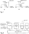
- Fig. 7 illustrates the effect of an interferer on the base-band radar signal in the frequency domain, in which the detection of radar targets is usually performed (e.g. using Range-Doppler Processing).
- the frequency of the interferer (relative to the frequency of the radar signal radiated by the own radar sensor) changes and the spectral line representing the interferer moves into the frequency band B, causing the interference shown, for example, in Fig. 6 .
- Diagram (b) on the right side of Fig. 7 illustrates this situation in which the interferer signal has moved into the frequency band B of the radar receiver. This situation is similar to the situation that arises at a time t 0 + ⁇ T of, e.g., 42 ⁇ s illustrated in the example of Fig. 5 .
- the examples discussed further below aim to detect the interferer earlier, if possible before the interferer enters the frequency band B of the radar receiver.
- Fig. 8 is a block diagram that illustrates an exemplary structure of radar sensor 1.
- At least one transmission antenna 5 (TX antenna(s)) and at least one reception antenna 6 (RX antenna(s)) are connected to an RF frontend 10, which may be integrated in a semiconductor chip, usually referred to as monolithic microwave integrated circuit (MMIC) 100.
- MMIC monolithic microwave integrated circuit
- the RF frontend 10 may include all of the circuit components needed for RF signal processing.
- Such circuit components may include, for example, a local oscillator (LO), RF power amplifiers, low noise amplifiers (LNAs), directional couplers such as rat-race-couplers and circulators, and mixers for the down-conversion of RF signals (e.g. the received signal y RF (t), see Fig. 1 ) in the base-band or IF-band.
- LO local oscillator
- LNA low noise amplifier
- directional couplers such as rat-race-couplers and circulators
- mixers for the down-conversion of RF signals (e.g. the received signal y RF (t), see Fig. 1 ) in the base-band or IF-band.
- antenna-arrays may be used instead of single antennas.
- the depicted example shows a bistatic (or pseudo-monostatic) radar system, which has separate RX and TX antennas.
- a single antenna or a single antenna array may be used for both, receiving and transmitting electromagnetic (
- the RF signals radiated by the TX antenna 5 may be in a range of between approximately 20 GHz (e.g. 24 GHz) and 81 GHz (e.g. about 77 GHz in automotive applications).
- the RF signal received by the RX antenna 6 includes the radar echoes, i.e. the signals that have been back-scattered at the radar target(s).
- the received RF signal y RF (t) is down-converted into the base band and is further processed in the base-band using analog signal processing (see Fig.
- base-band signal processing chain 20 which basically includes filtering and amplification of the base-band signal and thus determines the bandwidth of the received signal (cf. Fig. 5 , bandwidth B).
- the base-band signal is finally digitized using one or more analog-to-digital converters 30 and is then further processed in the digital domain (see Fig. 3 , digital signal processing chain implemented, e.g., in digital signal processor 40).
- the overall system is controlled by a system controller 50, which may be at least partly implemented in a processor which can execute appropriate firmware.
- the processor may be included, e.g. in a microcontroller, a digital signal processor, or the like.
- the digital signal processor 40 may be part of the system controller 50 or separate therefrom.
- the digital signal processor 40 may be partly implemented using hard-wired or one-time programmable logic circuitry and partly using a processor executing software (firmware). Alternatively, the digital signal processor may be substantially implemented using a processor programmed with software/firmware to perform the functions described herein. It is noted that the components shown in Fig. 8 may, in some examples, be integrated in a single semiconductor chip. For example, the RF frontend 10 and the analog baseband signal processing chain 20 and, in some examples, the ADC 30, the signal processor 40 and the system controller 50 may be integrated into a single MMIC to form a single chip radar system. However, the components may also be distributed among two or more integrated circuits.
- Fig. 9 illustrates one example of the RF frontend 10, which may be included in the radar sensor shown in Fig. 8 . It is noted that Fig. 9 is a simplified circuit diagram illustrating the basic structure of an RF frontend. Actual implementations, which may depend on the application, may be more complex. In particular, many practical implementations include multiple reception and transmission channels, wherein only one reception channel and one transmission channel is shown in the depicted example in order to keep the illustration simple.
- the RF frontend 10 includes a local oscillator (LO) 101 that generates a RF signal s LO (t), which may be frequency-modulated as explained above with reference to Figs. 2 and 4 .
- the signal s LO (t) is also referred to as LO signal).
- the LO signal is usually in the SHF (Super High Frequency) or the EHF (Extremely High Frequency) band, e.g. between 76 GHz and 81 GHz in automotive applications.
- the LO signal s LO (t) is processed in the transmitted signal path (transmission channel, TX channel), as well as in the receive signal path (reception channel, RX channel).
- the transmit signal s RF (t) which is radiated by the TX antenna 5, is generated by amplifying the (frequency-modulated) LO signal s LO (t), e.g., using an RF power amplifier 102.
- the output of the amplifier 102 is coupled to the TX antenna 5 e.g. via strip lines, a coupler, matching network, etc. (not shown in Fig. 9 ).
- the received signal y RF (t) which is provided by the RX antenna 6, is provided to a mixer 104.
- the received signal y RF (t) (i.e. the antenna signal) is pre-amplified by RF amplifier 103 (e.g. by a low-noise amplifier, LNA, with gain g), so that the mixer receives the amplified signal g ⁇ y RF (t) at its RF input.
- the mixer 104 further receives the frequency-modulated LO signal s LO (t) at its reference input and is configured to down-convert the amplified signal g ⁇ y RF (t) into the base band.
- the resulting base-band signal at the mixer output is denoted as y BB (t).
- the base-band signal y BB (t) is further processed by the analog base band signal processing chain 20 (see also Fig.
- the analog output signal of the base-band signal processing chain 20 is denoted as y(t) and may be supplied to an analog-to-digital converter (ADC) 30 (see also Fig. 8 ).
- ADC analog-to-digital converter
- the digital signal y[n] output by the ADC 30 is referred to as digital radar signal and includes the digital radar data.
- the digital radar signal may be supplied to a processor such as digital signal processor 40, which is programmed to further process the digital radar signal, e.g. by applying algorithms summarized as Range/Doppler processing.
- the implementation of the circuit components shown in Fig. 9 are as such known in the field of radar sensors and is thus not explained in more detail.
- Fig. 9 also illustrates how a desired radar echo and a radar signal transmitted by another radar sensor interfere with each other.
- Fig. 9 further shows the radar frontend 10' of a further radar sensor, wherein only the local oscillator 101' and the transmission channel (including amplifier 102') and the transmission antenna 5' are shown in order to keep the illustration simple.
- the further radar sensor radiates a signal s RF '(t).
- the resulting RF signal arriving at the reception antenna 6 of the first radar sensor is denoted as RF interference signal y RF,I (t).
- the reception antenna 6 of the first radar sensor receives the RF interference signal y RF,I (t) together with the desired RF echo signal y RF,T (t) caused by the radar target T at which the signal s RF (t) radiated by the first radar sensor is back-scattered.
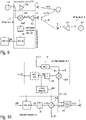
- Fig. 10 illustrates a first example which allows, at least in some situations, the detection of an interferer signal component generated outside of the MMIC (e.g. by another radar system) and received by a reception antenna before the signal is (e.g. digitally) processed in the baseband.
- the circuit of Fig. 10 illustrates a reception channel RX1 with a mixer 104 that receives the LO signal s LO (t) generated by the local oscillator and an RF signal y RF (t) received by antenna 6.
- the resulting baseband signal y BB (t) is further processed by the analog base band signal processing chain 20, and the analog output signal y(t) of the baseband signal processing chain 20 is supplied to ADC 30.
- the reception channel RX1 is basically identical to the example of Fig.
- a directional coupler 106 is inserted between the antenna port and the RF input of the reception channel RX1, which corresponds to the RF input port of the mixer 104 in the depicted example.
- the directional coupler 106 is configured to direct the signal y RF (t) received from antenna 109 to the mixer 104 and to divert a portion of the received signal power of signal y RF (t) to an additional auxiliary channel AUX. That is, the auxiliary channel is connected to the reverse signal port of the coupler at which the signal incident at the antenna port is output.
- the signal diverted from the reception channel RX1 is denoted as y RF,AUX (t) in Fig. 10 .
- the directional coupler 106 is configured to operate and couple RF signals in the range above 24 GHz, e.g. in the range of 76 to 81 GHz or above.
- the auxiliary channel AUX is constructed to receive and process RF signals similarly to other reception channels of the MMIC 100 (e.g. reception channel RX1) and therefore also includes a signal processing chain of a mixer 304, an analog base-band signal processing chain 320 and an ADC 330 configured to digitize the base-band signal y AUX (t) provided by the signal processing chain 320 at its output.
- the bandwidth of the signal processing chain 320 may be the same as the bandwidth B of the signal processing chain 20 of the reception channel RX1.
- the mixer 304 receives, at the RF port of the mixer, the RF signal y RF,AUX (t) diverted from the reception channel RX1 by the coupler 106. Different from a "normal" reception channel, a frequency shifted LO signal s LO,AUX (t) is supplied to the reference port of mixer 304 and used to down-convert the RF signal y RF,AUX (t) into the base band according to one example.
- the frequency of the LO signal s LO (t) is f LO
- the frequency of the frequency-shifted (auxiliary) LO signal s LO,AUX (t) is f LO + ⁇ f.
- the frequency shifted LO signal s LO,AUX (t) can be generated based on LO signal s LO (t) by modulating the LO signal s LO (t) with a sinusoidal signal that has a frequency equal to the frequency offset ⁇ f. Therefore, in the present example, the auxiliary channel AUX includes a modulator 305, which receives the LO signal s LO (t) and is configured to modulate the LO signal s LO (t) using a modulation signal which has a frequency equal to the frequency offset ⁇ f.
- the output signal of the modulator 305 is the frequency shifted LO signal s LO,AUX (t). Suitable modulators are known and thus not discussed herein in greater detail.
- the modulator is an IQ-modulator.
- the frequency offset ⁇ f between the signals s LO (t) and s LO,AUX (t) may be positive or negative.
- the frequency bands (e.g. of band width B) of the digital output signals y[n] and y AUX [n] of the reception channel RX1 and, respectively, the auxiliary channel AUX have a frequency offset equal to ⁇ f.
- the output signal y AUX [n] of the auxiliary channel AUX is in the frequency band B AUX which has also the bandwidth B but is frequency shifted (with respect to the frequency band B RX ) by the frequency offset ⁇ f. Accordingly, the interferer signal is detectable in the signal y AUX [n] while being absent from (and thus not detectable in) the output signal y[n] of reception channel RX1 in the depicted situation. Therefore, the presence of an interferer can be detected using the signal y AUX (t) or its digital representation y AUX [n].
- the frequency offset ⁇ f is approximately B/2, i.e. half the bandwidth of the frequency bands B RX and B AUX .
- the auxiliary channel AUX may be constructed such that the bandwidth of the frequency band B AUX is greater than the bandwidth of the frequency band B RX .
- the requirements concerning linearity e.g. linearity of the ADC
- linearity may be less strict for the auxiliary channel AUX than the requirements for a normal reception signal, where linearity is paramount for a precise detection of radar targets. Therefore, in the examples the auxiliary channel is not a copy of the reception channel, although the same functional components (e.g. ADCs 30, 330, Filters 20, 320) may be implemented in the auxiliary channel AUX and reception channel.
- the auxiliary channel may take up less area on the silicon chip.
- the depicted circuit includes an analog detector circuit 400 which is configured to detect an interferer signal (cf. Fig. 11 ) based on the analog signal y AUX (t) provided at the output of the analog signal processing chain 320.
- the analog detector circuit 400 may use one or more threshold values to detect an interferer in the time domain.
- the detector circuit 400 may modify the characteristics of one or more of the following elements of the reception channel RX1: the mixer 104, the signal processing chain 20, and the ADC 30.
- the detector circuit 400 may modify the gain of the mixer 104. With a reduced gain the mixer 104 is less likely to saturate.
- a saturated mixer output makes detection of a radar target almost impossible, wherein detection of a target may still be possible in the presence of an interferer if saturation is avoided.
- the detector circuit 400 is able to "look" ahead for a short period of time, which, however, is sufficiently long for the analog detector circuit to react and trigger suitable countermeasures such as, for example, reducing the gain of the mixer 104.
- a frequency offset ⁇ f of 20 MHz is necessary for a look-ahead time of 1 ⁇ s.
- Fig. 12 is a circuit diagram illustrating another example of an RF frontend with an auxiliary channel AUX for detecting an interferer signal.
- the present example is very similar to the previous example of Fig. 10 .
- the RF input signal y RF,AUX (t) of the auxiliary channel AUX is diverted from the antenna port of the transmission channel TX1 (using a directional coupler) instead of from the antenna port of the reception channel RX1 (as it is the case in Fig. 10 ).
- the directional coupler 106 which may be, for example, a rat-race coupler, a circulator, or the like, is connected between the RF output of the transmission channel TX1 of the radar device and the respective transmission antenna 5.
- the transmission channel TX1 also includes the RF power amplifier 102 (cf. Fig. 9 ) for amplifying the LO signal s LO (t) which is then directed to the antenna port by the directional coupler 106.
- the transmission antenna 5 is connected to the antenna port of the transmission channel and radiates the radar signal SRF (t) (amplified LO signal).
- an interferer signal (cf. signal y RF,I (t) in Fig. 9 ) can be received by the transmission antenna 5, as can any other RF signal.
- the signal received from the transmission antenna 5 is not dissipated in a termination resistance but is directed to the auxiliary channel AUX by the directional coupler 106.
- the received signal diverted from the transmission channel TX1 and received by the auxiliary channel is denoted as y RF,AUX (t).
- the auxiliary channel RX1 and the analog detector 400 operate in the same way as described above in connection with the previous example of Fig. 10 and reference is made to the respective description.
- the auxiliary channel AUX may differ from normal reception channels in some aspects.
- normal reception channels such as the reception channel RX1 need to be designed for a high linearity in order to allow for a precise detection of radar targets.
- the coupler 106 attenuates the interferer signal by approximately 15dB, the linearity requirements for the auxiliary channel can be lowered significantly.
- the auxiliary channel can be designed to have a significantly lower dynamic range than a normal reception channel because the detection of very small signals is not required for interference detection.
- the requirements concerning the signal to noise ratio at the output of the auxiliary channel are also significantly laxer than a normal reception channel.
- the laxer requirements for the auxiliary receiver allow for the integration of the auxiliary channel into a relatively small chip area (as compared to a normal reception channel). Accordingly, the auxiliary channel AUX will usually be integrated in the same MMIC as the normal reception channel(s). However, in some examples the auxiliary channel AUX may be implemented in a separate chip.
- the auxiliary channel AUX can be operated concurrently (operating at the same time) to the normal reception channel(s). That is, the detection of radar targets and the detection of interferer signals can be achieved in parallel (at the same time).
- the frequency offset ⁇ f introduced by the modulator in the auxiliary channel allows for an early detection of an interferer signal shortly before it disturbs / distorts the signal received by the normal reception channel(s).
- the achievable "look-ahead" time is proportional to the frequency offset ⁇ f. This look-ahead time allows the analog detector 400 to react before the interferer impairs the radar target detection.
- the frequency offset ⁇ f may be configurable or programmable, which allows for more flexibility in the implementation.
- the digital output signal y AUX [n] may be processed using, e.g. the digital signal processor 40 (cf. Fig. 8 )) in order to detect interferer signals.
- the digital signal processing for detecting interferer signals allows, for example, for the use of cognitive signal processing for the tracking and prediction of interferer signals. That is, the radar system can "learn” in which frequency bands interferences typically occur in specific situations, how often interferences occur, from which direction interferences are incident, etc.
- digital signal processing may be used to measure, based on the digital output signal y AUX [n] of the auxiliary channel AUX, at which power levels and for which duration a specific chirp is affected. Based upon this information, different interference mitigation techniques can be applied (e.g. discarding the whole chirp in the worst case or only making minor corrections to the chirp data in the best case).
- the auxiliary channel AUX and the reception channel RX1 can be operated simultaneously to concurrently detect interferer signals and radar targets.
- the auxiliary channel AUX is operated during the idle times of the reception channel RX1, i.e. between two subsequent acquisition sequences (see Fig. 4 , the time span between chirp sequences is labeled "1 st acquisition” and "2 nd acquisition”).
- the radar sensor can make use of an approach in which the radar channel is monitored for interference during idle times before an acquisition is started.
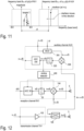
- a method for a radar system is illustrated in the flow chart in Fig. 13 . Accordingly, the method includes receiving - via a first RF port of a coupler (see, e.g. Fig. 10 or 12 , coupler 106) - an antenna signal y RF (t)) from an antenna ( Fig. 13 , step S1). The method further includes receiving - by an auxiliary receiver (see, e.g. Fig. 10 or 12 , auxiliary receiver AUX) - a representation of the antenna signal (e.g., Fig.
- an LO signal is generated e.g. by a local oscillator, and a frequency-shifting of the LO signal is performed by modulating the LO signal with a modulation signal which has a frequency equal to an offset frequency ⁇ f (cf. Fig. 10 or 12 , modulator 305).
- Generating the auxiliary base-band signal may include demodulating the mentioned representation of the antenna signal by mixing it with the frequency-shifted LO signal (cf. Fig. 10 or 12 , mixer 304).
- the method includes receiving - in a reception channel (see e.g. Fig. 10 or 12 , channel RX1) of the radar system - a further representation of the antenna signal via a third RF port of the coupler.
- the method includes generating - in a transmission channel (see e.g. Fig. 12 , channel TX1) of the radar system - an RF output signal based on the LO signal, wherein the RF output signal is supplied to a third port of the coupler (see Fig. 12 , coupler 106) which directs the RF output signal to the antenna.
- the signal power of the representation of the antenna signal received at the RF input of the reception channel is greater than a signal power of the representation of the antenna signal received by the auxiliary receiver ((see e.g. Fig. 10 , auxiliary channel AUX).
- n external radar interference signal may be performed using an analog circuit which has a control output coupled to the reception channel (see e.g. Fig. 10 or 12 , channel RX1), wherein the analog circuit may be configured to adjust the gain of one or more circuit components of the reception channel upon the detection of an interference.
Landscapes
- Engineering & Computer Science (AREA)
- Radar, Positioning & Navigation (AREA)
- Remote Sensing (AREA)
- Computer Networks & Wireless Communication (AREA)
- Physics & Mathematics (AREA)
- General Physics & Mathematics (AREA)
- Electromagnetism (AREA)
- Radar Systems Or Details Thereof (AREA)
Abstract
A radar system and a corresponding method for a radar system are described herein. In accordance with one example, the method includes receiving - via a first RF port of a coupler (106) - an antenna signal from an antenna (5,6), receiving - with an auxiliary receiver (AUX) - a representation of the antenna signal via a second RF port of the coupler, and generating - with the auxiliary receiver - an auxiliary base-band signal from the representation of the antenna signal. Based on the auxiliary base-band signal, an external radar interference signal transmitted from an external radar device incident at the antenna is detected.
Description
- The present disclosure relates to the field of radar sensors, in particular to radar sensing techniques that allow the detection of interfering RF signals.
- Radar sensors can be found in numerous sensing applications in which distances and velocities of objects are to be measured. In the automotive sector, there is an increasing demand for radar sensors that may be used in so-called advanced driver-assistance systems (ADAS). Examples of advanced driver assistive systems include "adaptive cruise control" (ACC) and "radar cruise control" systems. Such systems may be used to automatically adjust the speed of an automobile so as to maintain a safe distance from other automobiles driving ahead. Other examples of advanced driver assistive system are blind-spot monitors, which may employ radar sensors to detect other vehicles in the blind spot of a vehicle. Particularly autonomous cars may use numerous sensors, such as radar sensors, to detect and locate various objects in their surroundings. Information about the position and velocity of objects in the area of an autonomous car is used to help navigate safely.
- Modern radar systems make use of highly integrated RF circuits which may incorporate all core functions of an RF font-end of a radar transceiver in one single package (single chip transceiver). Such RF front-ends usually include, inter alia, a local RF oscillator (LO), power amplifiers (PA), low-noise amplifiers (LNA), and mixers. Frequency-modulated continuous-wave (FMCW) radar systems use radar signals whose frequency is modulated by ramping the signal frequency up and down. Such radar signals are often referred to as "chirp signals" or simply as "chirps". In case of linear chirp signals the term "LFM signals" is sometimes used, wherein LFM stands for "linear frequency modulation". A radar sensor usually radiates sequences of chirps using one or more antennas, and the radiated signal is backscattered by one or more objects (referred to as radar targets) located in the "field of view" of a radar sensor. The backscattered signals (radar echoes) are received and processed by the radar sensor. The detection of the radar targets is usually accomplished using digital signal processing.
- As more and more automobiles are being equipped with radar sensors, interference is becoming an issue. That is, the radar signal radiated by a first radar sensor (installed in one automobile) may intersperse to the reception antenna of a second radar sensor (installed in another automobile) and impair the operation of the second radar sensor. The inventors have identified the need for improvement of the interference detection in radar systems. Accordingly, the problem addressed by the examples described herein is the improvement of the interference detection in radar systems.
- The problem mentioned above is solved by the radar system of
claim 1 and the method ofclaim 10. Various examples and further developments are covered by the dependent claims. - A radar system is described herein. In accordance with one example, the system comprises an RF coupler that has a first RF port for receiving an RF antenna from an antenna, a second RF port configured to output a representation of the RF antenna signal, and a third RF port. The system further includes an auxiliary receiver channel having an RF input coupled to the second RF port of the RF coupler. The auxiliary receiver channel is configured to receive the representation of the RF antenna signal and is configured to generate an auxiliary base-band signal based on the representation of the RF antenna signal. Moreover, the system includes a detection circuit configured to detect, based on the auxiliary base-band signal, an external radar interference signal transmitted from an external radar device and incident at the antenna.
- Further, a method for a radar system is described herein. In accordance with one example, the method includes receiving - via a first RF port of a coupler - an antenna signal from an antenna, receiving - with an auxiliary receiver - a representation of the antenna signal via a second RF port of the coupler, and generating - with the auxiliary receiver - an auxiliary base-band signal from the representation of the antenna signal. Based on the auxiliary base-band signal, an external radar interference signal transmitted from an external radar device incident at the antenna is detected.
- The invention can be better understood with reference to the following drawings and descriptions. The components in the figures are not necessarily to scale; instead emphasis is placed upon illustrating the principles of the invention. In the figures, like reference numerals designate corresponding parts. In the drawings:
-
Figure 1 is a sketch illustrating the operating principle of an FMCW radar system for distance and/or velocity measurement. -
Figure 2 includes two timing diagrams illustrating the frequency modulation of the RF signal used in FMCW radar systems. -
Figure 3 illustrates one example of how interference is interspersed to the receiver of a radar sensor. -
Figure 4 is a timing diagram illustrating a sequence of chirps used for data acquisition in a radar sensor. -
Figure 5 illustrates in a timing diagram a transmitted signal of a radar sensor and an interference signal from an interferer, wherein the frequency-over-time waveforms of these signals at least partially overlap. -
Figure 6 illustrates one exemplary waveform including a radar signal (after down-conversion to the base band) including a radar echo from a target and interference as shown inFig. 5 . -
Figure 7 is a diagram illustrating how interference may affect the detection of radar targets or lead to the detection of so-called "ghost targets". -
Figure 8 is a block diagram illustrating the basic structure of an FMCW radar device. -
Figure 9 is a circuit diagram illustrating one example of an analog RF frontend of a radar sensor and an analog RF frontend of an interferer. -
Figure 10 is a circuit diagram illustrating one example of an RF frontend with an auxiliary channel for detecting an interferer signal. -
Figure 11 is a diagram visualizing, in a spectrum, function and purpose of the auxiliary channel in the example ofFig. 10 . -
Figure 12 is a circuit diagram illustrating another example of an RF frontend with an auxiliary channel for detecting an interferer signal. -
Figure 13 is a flow-chart illustrating one example of a method for a radar system. -
Fig. 1 illustrates a conventional frequency-modulated continuous-wave (FMCW)radar sensor 1. In the present example, separate transmission (TX) and reception (RX)antennas reception antenna 6. The object T is usually referred to as "radar target". - In a more general example, more than one target may be in the field of view of a radar sensor, and an antenna array may be used instead of a single RX antenna. Similarly, an antenna array may be used instead of a single TX antenna. Using multiple RX and TX antennas in a multi-channel radar system allows for the measurement of the angle of incidence of a radar echo, usually referred to as direction of arrival (DoA). Measuring the direction of arrival is important for many applications, and thus most radar sensors will make use of antenna arrays. To keep the drawings simple, only one TX antenna and one RX antenna (and respective TX and RX channels) are shown in the figures. It is understood that the concepts described herein are readily applicable to multi-channel radar sensors with antenna arrays, as well.
-
Fig. 2 illustrates the mentioned conventional frequency-modulation of the signal SRF(t). As shown in the top diagram ofFig, 2 , the signal SRF(t) is composed of a series of "chirps", i.e. sinusoidal waveforms with increasing (up-chirp) or decreasing (down-chirp) frequency. In the present example, the instantaneous frequency fLO(t) of a chirp increases linearly from a start frequency fSTART to a stop frequency fSTOP within a defined time span TCHIRP (see bottom diagram ofFig. 2 ). Such a chirp is also referred to as a linear frequency ramp. A linear frequency-modulated (LFM) signal with a sequence of three identical linear frequency ramps is illustrated inFig. 2 . It is noted, however, that the parameters fSTART, fSTOP, TCHIRP as well as the pause between the individual frequency ramps may vary dependent on the actual implementation of theradar device 1 and may also vary during operation of the radar device. In practice the frequency variation may be, for example, linear (linear chirp, frequency ramp), exponential (exponential chirp) or hyperbolic (hyperbolic chirp). -
Fig. 3 illustrates one simple example showing how interferers can disturb the operation of a radar sensor.Fig. 3 illustrates a road with three lanes and five vehicles A1, A2, A3, A4, and A5. In the present example, vehicle A1 is considered to be the "own vehicle" (ego vehicle) and its radar sensor as "own radar sensor". The own radar sensor transmits a signal and senses an echo signal E1 back-scattered from vehicle A5, which is the radar target T to be detected by the own radar sensor. However, in addition to the desired echo signal E1, the own radar sensor receives disturbing signals D2, D3, D4 transmitted by the on-board radar sensors of vehicles A2, A3 and A4. These disturbing signals interfere with the desired radar echo E1 and may negatively affect the detection of radar targets from the received radar signal (which includes the echo signal E1 and the disturbing signals D2, D3, and D4). -
Fig. 4 schematically illustrates an LFM signal with an exemplary FM scheme as is commonly implemented in FMCW radar sensors. In the depicted example, a sequence of sixteen up-chirps is transmitted for one data acquisition. It is noted that, in practice, a chirp sequence usually includes many more chirps (e.g. 256 chirps) and the present example has been simplified for illustration purposes only. A radar sensor transmits an LFM signal, such as depicted inFig.4 , and receives a respective radar echo signal. The detection of radar echoes is usually performed for each acquisition (i.e. chirp sequence for chirp sequence). Suitable signal processing methods are, for example, Range-Doppler Processing or Range-Doppler Analysis. - Dependent on the characteristics of the interfering signals (cf.
Fig. 3 , signals D2, D3, and D4), the desired radar echoes may be affected in different ways.Figs. 5 and 6 illustrate examples of how an interferer may disturb the received radar echoes when the interfering signals include chirps that have different parameters, particularly a different frequency slope, than those of the desired radar echoes.Fig. 6 illustrates the frequency over time of one chirp (solid line,chirp duration 60 µs) radiated by the own radar sensor in the example ofFig. 3 . The start frequency of the radiated signal SRF(t) is approximately 76250 MHz and the stop frequency is approximately 76600 MHz. An interference signal (e.g. disturbing signal D3 in the example ofFig. 3 ) generated by another radar sensor includes an up-chirp which starts at approximately 76100 MHz and stops at 76580 MHz (chirp duration 30 µs) and a subsequent down-chirp which starts at the stop frequency of the preceding up-chirp (76580 MHz) and stops at the start frequency of the next up-chirp (76100 MHz), which has a chirp duration of 10 µs. The bandwidth B of the base band signal of the own radar sensor is indicated inFig. 5 by the dashed lines. -
Fig. 6 illustrates an exemplary waveform of the (pre-processed) base band signal resulting from the received radar signal and including a desired radar echo, as well as interference. One can see that the signal components resulting from the interference have a significant magnitude in those time intervals in which the frequency of the interference signal is within the bandwidth B of the radar sensor (seeFig. 5 ). In the present example, the interference occurs three times during the 60 µs chirp duration, namely at approximately 7 µs, 28 µs and 42 µs (where the chirp slopes shown inFig. 5 intersect). As mentioned, the power of interference signals is usually higher than the power of radar echoes from real targets. Nevertheless, interferences appear as comparably short bursts whose duration corresponds to the time during which the bandwidths of the signals overlap. Therefore, not all chirps of one acquisition sequence (seeFig, 4 ) are usually affected by interference. Further, interference signals and the transmitted signal of a specific radar sensor are, in the present example, uncorrelated and thus the interference can be regarded as noise which increases the overall noise floor. -
Fig. 7 illustrates the effect of an interferer on the base-band radar signal in the frequency domain, in which the detection of radar targets is usually performed (e.g. using Range-Doppler Processing). Diagram (a) on the left side ofFig. 7 illustrates three radar targets Ti (i=1, 2, 3) present within the bandwidth B of the baseband of the considered own radar sensor, wherein an interferer is outside the bandwidth B. This situation is similar to the situation that arises at a time to of, e.g., 40 µs illustrated in the example ofFig. 5 . However, the frequency of the interferer (relative to the frequency of the radar signal radiated by the own radar sensor) changes and the spectral line representing the interferer moves into the frequency band B, causing the interference shown, for example, inFig. 6 . Diagram (b) on the right side ofFig. 7 illustrates this situation in which the interferer signal has moved into the frequency band B of the radar receiver. This situation is similar to the situation that arises at a time t0+ΔT of, e.g., 42 µs illustrated in the example ofFig. 5 . The examples discussed further below aim to detect the interferer earlier, if possible before the interferer enters the frequency band B of the radar receiver. - Before discussing the examples in more detail, the generic structure of an example of a radar system will be described.
Fig. 8 is a block diagram that illustrates an exemplary structure ofradar sensor 1. At least one transmission antenna 5 (TX antenna(s)) and at least one reception antenna 6 (RX antenna(s)) are connected to anRF frontend 10, which may be integrated in a semiconductor chip, usually referred to as monolithic microwave integrated circuit (MMIC) 100. TheRF frontend 10 may include all of the circuit components needed for RF signal processing. Such circuit components may include, for example, a local oscillator (LO), RF power amplifiers, low noise amplifiers (LNAs), directional couplers such as rat-race-couplers and circulators, and mixers for the down-conversion of RF signals (e.g. the received signal yRF(t), seeFig. 1 ) in the base-band or IF-band. As mentioned, antenna-arrays may be used instead of single antennas. The depicted example shows a bistatic (or pseudo-monostatic) radar system, which has separate RX and TX antennas. In the case of a monostatic radar system, a single antenna or a single antenna array may be used for both, receiving and transmitting electromagnetic (radar) signals. In this case a directional coupler (e.g. a circulator) may be used to separate RF signals to be transmitted to the radar channel from RF signals received from the radar channel. - In the case of a frequency-modulated continuous-wave (FMCW) radar sensor, the RF signals radiated by the
TX antenna 5 may be in a range of between approximately 20 GHz (e.g. 24 GHz) and 81 GHz (e.g. about 77 GHz in automotive applications). As mentioned, the RF signal received by theRX antenna 6 includes the radar echoes, i.e. the signals that have been back-scattered at the radar target(s). The received RF signal yRF(t) is down-converted into the base band and is further processed in the base-band using analog signal processing (seeFig. 8 , base-band signal processing chain 20), which basically includes filtering and amplification of the base-band signal and thus determines the bandwidth of the received signal (cf.Fig. 5 , bandwidth B). The base-band signal is finally digitized using one or more analog-to-digital converters 30 and is then further processed in the digital domain (seeFig. 3 , digital signal processing chain implemented, e.g., in digital signal processor 40). The overall system is controlled by asystem controller 50, which may be at least partly implemented in a processor which can execute appropriate firmware. The processor may be included, e.g. in a microcontroller, a digital signal processor, or the like. The digital signal processor 40 (DSP) may be part of thesystem controller 50 or separate therefrom. Thedigital signal processor 40 may be partly implemented using hard-wired or one-time programmable logic circuitry and partly using a processor executing software (firmware). Alternatively, the digital signal processor may be substantially implemented using a processor programmed with software/firmware to perform the functions described herein. It is noted that the components shown inFig. 8 may, in some examples, be integrated in a single semiconductor chip. For example, theRF frontend 10 and the analog basebandsignal processing chain 20 and, in some examples, theADC 30, thesignal processor 40 and thesystem controller 50 may be integrated into a single MMIC to form a single chip radar system. However, the components may also be distributed among two or more integrated circuits. -
Fig. 9 illustrates one example of theRF frontend 10, which may be included in the radar sensor shown inFig. 8 . It is noted thatFig. 9 is a simplified circuit diagram illustrating the basic structure of an RF frontend. Actual implementations, which may depend on the application, may be more complex. In particular, many practical implementations include multiple reception and transmission channels, wherein only one reception channel and one transmission channel is shown in the depicted example in order to keep the illustration simple. TheRF frontend 10 includes a local oscillator (LO) 101 that generates a RF signal sLO(t), which may be frequency-modulated as explained above with reference toFigs. 2 and4 . The signal sLO(t) is also referred to as LO signal). In radar applications, the LO signal is usually in the SHF (Super High Frequency) or the EHF (Extremely High Frequency) band, e.g. between 76 GHz and 81 GHz in automotive applications. - The LO signal sLO(t) is processed in the transmitted signal path (transmission channel, TX channel), as well as in the receive signal path (reception channel, RX channel). The transmit signal sRF(t), which is radiated by the
TX antenna 5, is generated by amplifying the (frequency-modulated) LO signal sLO(t), e.g., using anRF power amplifier 102. The output of theamplifier 102 is coupled to theTX antenna 5 e.g. via strip lines, a coupler, matching network, etc. (not shown inFig. 9 ). The received signal yRF(t), which is provided by theRX antenna 6, is provided to amixer 104. In the present example, the received signal yRF(t) (i.e. the antenna signal) is pre-amplified by RF amplifier 103 (e.g. by a low-noise amplifier, LNA, with gain g), so that the mixer receives the amplified signal g·yRF(t) at its RF input. Themixer 104 further receives the frequency-modulated LO signal sLO(t) at its reference input and is configured to down-convert the amplified signal g·yRF(t) into the base band. The resulting base-band signal at the mixer output is denoted as yBB(t). The base-band signal yBB(t) is further processed by the analog base band signal processing chain 20 (see alsoFig. 8 ), which basically includes one or more filters (e.g. a band-pass or a low-pass) for removing undesired side bands and image frequencies, as well as one or more amplifiers. The analog output signal of the base-bandsignal processing chain 20 is denoted as y(t) and may be supplied to an analog-to-digital converter (ADC) 30 (see alsoFig. 8 ). The digital signal y[n] output by theADC 30 is referred to as digital radar signal and includes the digital radar data. The digital radar signal may be supplied to a processor such asdigital signal processor 40, which is programmed to further process the digital radar signal, e.g. by applying algorithms summarized as Range/Doppler processing. The implementation of the circuit components shown inFig. 9 are as such known in the field of radar sensors and is thus not explained in more detail. -
Fig. 9 also illustrates how a desired radar echo and a radar signal transmitted by another radar sensor interfere with each other.Fig. 9 further shows the radar frontend 10' of a further radar sensor, wherein only the local oscillator 101' and the transmission channel (including amplifier 102') and the transmission antenna 5' are shown in order to keep the illustration simple. The further radar sensor radiates a signal sRF'(t). The resulting RF signal arriving at thereception antenna 6 of the first radar sensor is denoted as RF interference signal yRF,I(t). Thereception antenna 6 of the first radar sensor receives the RF interference signal yRF,I(t) together with the desired RF echo signal yRF,T(t) caused by the radar target T at which the signal sRF(t) radiated by the first radar sensor is back-scattered. - Both, the radar echo yRF,T(t) and the interference signal yRF,I(t) are received by the
antenna 6 and superpose each other at the RF input of mixer 104 (yRF(t)= yRF,T(t)+yRF,I(t)). It can be seen fromFig. 9 that the interference signal component yRF,I(t) of the received signal yRF(t) is down-converted into the base band in the same way as radar echoes yRF,T(t) included in the received signal yRF(t). Accordingly, when the frequency difference between the instantaneous frequency fLO of the transmit signal sRF(t) and the instantaneous frequency of the received interference signal yRF,I(t) lies within the bandwidth B of the base-bandsignal processing chain 20, interference will also be present in the digital signal y[n]. - Various approaches to mitigate or cancel interference are known. However, in order to mitigate or cancel interferer signal components, the presence of an interferer signal component needs first to be detected.
Fig. 10 illustrates a first example which allows, at least in some situations, the detection of an interferer signal component generated outside of the MMIC (e.g. by another radar system) and received by a reception antenna before the signal is (e.g. digitally) processed in the baseband. - The circuit of
Fig. 10 illustrates a reception channel RX1 with amixer 104 that receives the LO signal sLO(t) generated by the local oscillator and an RF signal yRF(t) received byantenna 6. The resulting baseband signal yBB(t) is further processed by the analog base bandsignal processing chain 20, and the analog output signal y(t) of the basebandsignal processing chain 20 is supplied toADC 30. In the depicted example, the reception channel RX1 is basically identical to the example ofFig. 9 , except that theLNA 103 has been omitted (in order to keep the illustration simple) and adirectional coupler 106 is inserted between the antenna port and the RF input of the reception channel RX1, which corresponds to the RF input port of themixer 104 in the depicted example. Thedirectional coupler 106 is configured to direct the signal yRF(t) received from antenna 109 to themixer 104 and to divert a portion of the received signal power of signal yRF(t) to an additional auxiliary channel AUX. That is, the auxiliary channel is connected to the reverse signal port of the coupler at which the signal incident at the antenna port is output. The signal diverted from the reception channel RX1 is denoted as yRF,AUX(t) inFig. 10 . In some examples, thedirectional coupler 106 is configured to operate and couple RF signals in the range above 24 GHz, e.g. in the range of 76 to 81 GHz or above. - The auxiliary channel AUX is constructed to receive and process RF signals similarly to other reception channels of the MMIC 100 (e.g. reception channel RX1) and therefore also includes a signal processing chain of a
mixer 304, an analog base-bandsignal processing chain 320 and anADC 330 configured to digitize the base-band signal yAUX(t) provided by thesignal processing chain 320 at its output. The bandwidth of thesignal processing chain 320 may be the same as the bandwidth B of thesignal processing chain 20 of the reception channel RX1. - The
mixer 304 receives, at the RF port of the mixer, the RF signal yRF,AUX(t) diverted from the reception channel RX1 by thecoupler 106. Different from a "normal" reception channel, a frequency shifted LO signal sLO,AUX(t) is supplied to the reference port ofmixer 304 and used to down-convert the RF signal yRF,AUX(t) into the base band according to one example. The frequency of the LO signal sLO(t) is fLO, whereas the frequency of the frequency-shifted (auxiliary) LO signal sLO,AUX(t) is fLO+Δf. - The frequency shifted LO signal sLO,AUX(t) can be generated based on LO signal sLO(t) by modulating the LO signal sLO(t) with a sinusoidal signal that has a frequency equal to the frequency offset Δf. Therefore, in the present example, the auxiliary channel AUX includes a
modulator 305, which receives the LO signal sLO(t) and is configured to modulate the LO signal sLO(t) using a modulation signal which has a frequency equal to the frequency offset Δf. The output signal of themodulator 305 is the frequency shifted LO signal sLO,AUX(t). Suitable modulators are known and thus not discussed herein in greater detail. In one example, the modulator is an IQ-modulator. The frequency offset Δf between the signals sLO(t) and sLO,AUX(t) may be positive or negative. As a consequence, the frequency bands (e.g. of band width B) of the digital output signals y[n] and yAUX[n] of the reception channel RX1 and, respectively, the auxiliary channel AUX, have a frequency offset equal to Δf. - The diagram of
Fig. 11 illustrates the effect of the frequency offset Δf. Similar to diagram (a) ofFig. 7 ,Fig. 11 illustrates the digital output signal y[n] of reception channel RX1, which includes three radar targets Ti (i=1, 2, 3) in a frequency band BRX of bandwidth B, which is basically determined by the band-pass characteristics of the analog signal processing chain 20 (cf.Fig. 10 ).Fig. 11 also shows a spectral line illustrating an interferer signal, which is outside of the frequency band BRX and thus does not (yet) affect the digital radar signal y[n] and the detection of the radar targets Ti. However, for FMCW, the interferer (to be precise: the spectral line caused by the interferer signal) is "moving" towards the frequency band BRX and will disturb the digital radar signal y[n] some short time later. - However, the output signal yAUX[n] of the auxiliary channel AUX is in the frequency band BAUX which has also the bandwidth B but is frequency shifted (with respect to the frequency band BRX) by the frequency offset Δf. Accordingly, the interferer signal is detectable in the signal yAUX[n] while being absent from (and thus not detectable in) the output signal y[n] of reception channel RX1 in the depicted situation. Therefore, the presence of an interferer can be detected using the signal yAUX(t) or its digital representation yAUX[n]. In one example the frequency offset Δf is approximately B/2, i.e. half the bandwidth of the frequency bands BRX and BAUX. It is understood that the auxiliary channel AUX may be constructed such that the bandwidth of the frequency band BAUX is greater than the bandwidth of the frequency band BRX. Further, it is noted that the requirements concerning linearity (e.g. linearity of the ADC) may be less strict for the auxiliary channel AUX than the requirements for a normal reception signal, where linearity is paramount for a precise detection of radar targets. Therefore, in the examples the auxiliary channel is not a copy of the reception channel, although the same functional components (
e.g. ADCs Filters 20, 320) may be implemented in the auxiliary channel AUX and reception channel. In some examples, the auxiliary channel may take up less area on the silicon chip. - Referring again to
Fig. 10 , the depicted circuit includes ananalog detector circuit 400 which is configured to detect an interferer signal (cf.Fig. 11 ) based on the analog signal yAUX(t) provided at the output of the analogsignal processing chain 320. For this purpose, theanalog detector circuit 400 may use one or more threshold values to detect an interferer in the time domain. Upon detection of an interferer that is moving towards the frequency band BRX, thedetector circuit 400 may modify the characteristics of one or more of the following elements of the reception channel RX1: themixer 104, thesignal processing chain 20, and theADC 30. For example, thedetector circuit 400 may modify the gain of themixer 104. With a reduced gain themixer 104 is less likely to saturate. A saturated mixer output makes detection of a radar target almost impossible, wherein detection of a target may still be possible in the presence of an interferer if saturation is avoided. - It should be noted that, due to the frequency offset Δf discussed above, the
detector circuit 400 is able to "look" ahead for a short period of time, which, however, is sufficiently long for the analog detector circuit to react and trigger suitable countermeasures such as, for example, reducing the gain of themixer 104. According to one example, in which the RF chirps have a steepness of 20 MHz/µs, a frequency offset Δf of 20 MHz is necessary for a look-ahead time of 1 µs. In one example, the bandwidth B of the reception channel RX1 is equal to Δf (e.g. B= Δf=20 MHz). -
Fig. 12 is a circuit diagram illustrating another example of an RF frontend with an auxiliary channel AUX for detecting an interferer signal. The present example is very similar to the previous example ofFig. 10 . However, according toFig. 5 , the RF input signal yRF,AUX(t) of the auxiliary channel AUX is diverted from the antenna port of the transmission channel TX1 (using a directional coupler) instead of from the antenna port of the reception channel RX1 (as it is the case inFig. 10 ). - In the example of
Fig. 12 , thedirectional coupler 106, which may be, for example, a rat-race coupler, a circulator, or the like, is connected between the RF output of the transmission channel TX1 of the radar device and therespective transmission antenna 5. The transmission channel TX1 also includes the RF power amplifier 102 (cf.Fig. 9 ) for amplifying the LO signal sLO(t) which is then directed to the antenna port by thedirectional coupler 106. Thetransmission antenna 5 is connected to the antenna port of the transmission channel and radiates the radar signal SRF(t) (amplified LO signal). - Although the
transmission antenna 5 is configured for and operates by transmitting signals, an interferer signal (cf. signal yRF,I(t) inFig. 9 ) can be received by thetransmission antenna 5, as can any other RF signal. Different from other implementations, the signal received from thetransmission antenna 5 is not dissipated in a termination resistance but is directed to the auxiliary channel AUX by thedirectional coupler 106. The received signal diverted from the transmission channel TX1 and received by the auxiliary channel is denoted as yRF,AUX(t). The auxiliary channel RX1 and theanalog detector 400 operate in the same way as described above in connection with the previous example ofFig. 10 and reference is made to the respective description. - Irrespective of the specific implementation (e.g. according to
Fig. 10 or12 ), the auxiliary channel AUX (auxiliary receiver) may differ from normal reception channels in some aspects. For example, normal reception channels such as the reception channel RX1 need to be designed for a high linearity in order to allow for a precise detection of radar targets. As the coupler 106 (seeFig. 10 or12 ) attenuates the interferer signal by approximately 15dB, the linearity requirements for the auxiliary channel can be lowered significantly. Furthermore, the auxiliary channel can be designed to have a significantly lower dynamic range than a normal reception channel because the detection of very small signals is not required for interference detection. Moreover, the requirements concerning the signal to noise ratio at the output of the auxiliary channel are also significantly laxer than a normal reception channel. The laxer requirements for the auxiliary receiver allow for the integration of the auxiliary channel into a relatively small chip area (as compared to a normal reception channel). Accordingly, the auxiliary channel AUX will usually be integrated in the same MMIC as the normal reception channel(s). However, in some examples the auxiliary channel AUX may be implemented in a separate chip. - As can be seen in
Figs. 10-12 , the auxiliary channel AUX can be operated concurrently (operating at the same time) to the normal reception channel(s). That is, the detection of radar targets and the detection of interferer signals can be achieved in parallel (at the same time). As discussed above, the frequency offset Δf introduced by the modulator in the auxiliary channel (seeFig. 10 and12 , modulator 305) allows for an early detection of an interferer signal shortly before it disturbs / distorts the signal received by the normal reception channel(s). The achievable "look-ahead" time is proportional to the frequency offset Δf. This look-ahead time allows theanalog detector 400 to react before the interferer impairs the radar target detection. In some embodiments, the frequency offset Δf may be configurable or programmable, which allows for more flexibility in the implementation. - In addition, or as an alternative to, the
analog detector 400, the digital output signal yAUX[n] may be processed using, e.g. the digital signal processor 40 (cf.Fig. 8 )) in order to detect interferer signals. The digital signal processing for detecting interferer signals allows, for example, for the use of cognitive signal processing for the tracking and prediction of interferer signals. That is, the radar system can "learn" in which frequency bands interferences typically occur in specific situations, how often interferences occur, from which direction interferences are incident, etc. Additionally or alternatively, digital signal processing may be used to measure, based on the digital output signal yAUX[n] of the auxiliary channel AUX, at which power levels and for which duration a specific chirp is affected. Based upon this information, different interference mitigation techniques can be applied (e.g. discarding the whole chirp in the worst case or only making minor corrections to the chirp data in the best case). - As mentioned, the auxiliary channel AUX and the reception channel RX1 can be operated simultaneously to concurrently detect interferer signals and radar targets. In another example, the auxiliary channel AUX is operated during the idle times of the reception channel RX1, i.e. between two subsequent acquisition sequences (see
Fig. 4 , the time span between chirp sequences is labeled "1st acquisition" and "2nd acquisition"). Accordingly, the radar sensor can make use of an approach in which the radar channel is monitored for interference during idle times before an acquisition is started. - In the following, the various approaches and techniques implemented in the examples described herein are summarized. It is, however, emphasized that the following is not an exhaustive list of technical features but rather an exemplary summary. A method for a radar system is illustrated in the flow chart in
Fig. 13 . Accordingly, the method includes receiving - via a first RF port of a coupler (see, e.g.Fig. 10 or12 , coupler 106) - an antenna signal yRF(t)) from an antenna (Fig. 13 , step S1). The method further includes receiving - by an auxiliary receiver (see, e.g.Fig. 10 or12 , auxiliary receiver AUX) - a representation of the antenna signal (e.g.,Fig. 10 or12 , signal yRF,AUX(t)) via a second RF port of the coupler (Fig. 13 , step S2) and generating - by the auxiliary receiver - an auxiliary baseband signal from the representation of the antenna signal (Fig. 13 , step S3). Based on the auxiliary base-band signal (see, e.g.,Fig. 10 or12 , signal yAUX(t)), an external radar interference signal transmitted from an external radar device incident at the antenna is detected (Fig. 13 , step S4). - In one example, an LO signal is generated e.g. by a local oscillator, and a frequency-shifting of the LO signal is performed by modulating the LO signal with a modulation signal which has a frequency equal to an offset frequency Δf (cf.
Fig. 10 or12 , modulator 305). Generating the auxiliary base-band signal (cf.Fig, 13 , step S3) may include demodulating the mentioned representation of the antenna signal by mixing it with the frequency-shifted LO signal (cf.Fig. 10 or12 , mixer 304). - In one example, the method includes receiving - in a reception channel (see e.g.
Fig. 10 or12 , channel RX1) of the radar system - a further representation of the antenna signal via a third RF port of the coupler. In one example, the method includes generating - in a transmission channel (see e.g.Fig. 12 , channel TX1) of the radar system - an RF output signal based on the LO signal, wherein the RF output signal is supplied to a third port of the coupler (seeFig. 12 , coupler 106) which directs the RF output signal to the antenna. - In the examples described herein, the signal power of the representation of the antenna signal received at the RF input of the reception channel (see e.g.
Fig. 10 , channel RX1) is greater than a signal power of the representation of the antenna signal received by the auxiliary receiver ((see e.g.Fig. 10 , auxiliary channel AUX). - The detection of n external radar interference signal (see
Fig. 13 , step 4) may be performed using an analog circuit which has a control output coupled to the reception channel (see e.g.Fig. 10 or12 , channel RX1), wherein the analog circuit may be configured to adjust the gain of one or more circuit components of the reception channel upon the detection of an interference. - Although the invention has been illustrated and described with respect to one or more implementations, alterations and/or modifications may be made to the illustrated examples without departing from the spirit and scope of the appended claims. In particular regard to the various functions performed by the above described components or structures (units, assemblies, devices, circuits, systems, etc.), the terms (including a reference to a "means") used to describe such components are intended to correspond - unless otherwise indicated - to any component or structure which performs the specified function of the described component (e.g., that is functionally equivalent), even though not structurally equivalent to the disclosed structure which performs the function in the herein illustrated exemplary implementations of the invention.
Claims (15)
- A radar device comprising:an RF coupler (106) having a first RF port for receiving an RF antenna signal (yRF(t)) from an antenna (5, 6); a second RF port configured to output a representation (yRF,AUX(t)) of the RF antenna signal (yRF(t)), and a third RF port;an auxiliary receiver (AUX) having an RF input coupled to the second RF port of the RF coupler (106); the auxiliary receiver (AUX) being configured to receive the representation (yRF,AUX(t)) of the RF antenna signal (yRF(t)) and configured to generate an auxiliary base-band signal (yAUX(t)) based on the representation (yRF,AUX(t)) of the RF antenna signal (yRF(t)); anda detection circuit (400) configured to detect, based on the auxiliary base-band signal (yAUX(t)), an external radar interference signal transmitted from an external radar device incident at the antenna (5, 6).
- The radar system of claim 1, further comprising:a modulator (MOD) configured to generate a first RF signal (sLO'(t)) by frequency-shifting an LO signal (sLO(t)) by an offset frequency (Δf),wherein the auxiliary channel (AUX) is configured to generate the auxiliary base-band signal (yAUX(t) based on the first RF signal (sLO'(t)).
- The radar device of claim 1, further comprising:a transmission channel (TX1) configured to receive an LO signal (sLO(t)), to generate an RF output signal (sRF(t)) based on the LO signal (sLO(t)), and to output the RF output signal (sRF(t)) at an RF output of the transmission channel (TX1).
- The radar system of claim 3,
wherein the auxiliary receiver (AUX) includes a mixer (304) configured to receive the representation (yRF,AUX(t)) of the RF antenna signal (yRF(t)) from the coupler (106) and the first RF signal (sLO'(t)), the mixer providing the auxiliary base-band signal (yAUX(t)) at its output. - The radar system of claim 3 or 4,wherein the third port of the RF coupler (106) is coupled to the RF output of the transmit channel (TX1), andwherein the RF coupler (106) is configured to direct the RF output signal (sRF(t)) to the antenna (5).
- The radar system of any of claims 1 to 5,
wherein the third port of the RF coupler (106) is coupled to an RF input of a reception channel (RX1) that is configured to receive, from the RF coupler (106), a further representation of the antenna signal (yRF(t)) at its RF input and to generate a receiver base-band radar signal (yBB(t)) from the further representation of the antenna signal (yRF(t)) using the LO signal (sLO(t)). - The radar system of claim 6,
wherein a signal power of the further representation of the antenna signal (yRF(t)) received at the RF input of the reception channel (RX1) is greater than a signal power of the representation (yRF,AUX(t)) of the antenna signal (yRF(t)) received by the auxiliary receiver (AUX). - The radar system of any of claims 1 to 5,
wherein the detection circuit (400) is an analog circuit having a control output coupled to a reception channel (RX1), the analog circuit being configured to adjust the gain of the receive channel (RX1) upon the detection of an interference. - The radar system of an of claims 1 to 5,wherein the auxiliary receiver (AUX) includes and analog-to-digital converter (330) configured to digitize the auxiliary base-band signal (yAUX(t)), andwherein the detection circuit includes a digital signal processing circuit configured to detect of an interference based on the digitized auxiliary base-band signal (yAUX[n]).
- A method for a radar device, the method comprising:receiving via a first RF port of a coupler (106) an antenna signal (yRF(t)) from an antenna (5, 6);receiving, by an auxiliary receiver (AUX), a representation (yRF,AUX(t)) of the antenna signal (yRF(t)) via a second RF port of the coupler (106);generating, by the auxiliary receiver (AUX), an auxiliary base-band signal (yAUX(t)) from the representation of the antenna signal (yRF,AUX(t)); anddetecting, based on the auxiliary base-band signal (yAUX(t)), an external radar interference signal transmitted from an external radar device incident at the antenna (5, 6).
- The method of claim 10, further comprising:generating an LO signal (sLO(t)); andfrequency-shifting the LO signal (sLO(t)) by modulating the LO signal (sLO(t)) with a modulation signal having a frequency equal to the offset frequency (Δf).
- The method of claim 11, wherein generating the auxiliary base-band signal (yAUX(t)) comprises:
demodulating the representation of the antenna signal (yRF,AUX(t)) by mixing it with the frequency-shifted LO signal (sLO'(t)). - The method of any of claims 10 to 12, further comprising:
receiving, by a reception channel (RX1), a further representation of the antenna signal (yRF(t)) via a third RF port of the coupler (106). - The method of any of claims 10 to 12, further comprising:generating, by a transmission channel (TX1), an RF output signal (sRF(t)) based on the LO signal (sLO(t)),wherein the RF output signal (sRF(t)) is supplied to a third port of the coupler (106), which directs the RF output signal to the antenna (5).
- The method of any of claims 10 to 14, further comprising:digitizing the base-band signal,wherein detecting an external radar interference signal includes processing the digitized base-band signal.
Priority Applications (2)
| Application Number | Priority Date | Filing Date | Title |
|---|---|---|---|
| EP21199046.0A EP4155756A1 (en) | 2021-09-27 | 2021-09-27 | Fmcw radar |
| US17/930,267 US20230097888A1 (en) | 2021-09-27 | 2022-09-07 | Fmcw radar |
Applications Claiming Priority (1)
| Application Number | Priority Date | Filing Date | Title |
|---|---|---|---|
| EP21199046.0A EP4155756A1 (en) | 2021-09-27 | 2021-09-27 | Fmcw radar |
Publications (1)
| Publication Number | Publication Date |
|---|---|
| EP4155756A1 true EP4155756A1 (en) | 2023-03-29 |
Family
ID=77951635
Family Applications (1)
| Application Number | Title | Priority Date | Filing Date |
|---|---|---|---|
| EP21199046.0A Pending EP4155756A1 (en) | 2021-09-27 | 2021-09-27 | Fmcw radar |
Country Status (2)
| Country | Link |
|---|---|
| US (1) | US20230097888A1 (en) |
| EP (1) | EP4155756A1 (en) |
Citations (4)
| Publication number | Priority date | Publication date | Assignee | Title |
|---|---|---|---|---|
| US6121918A (en) * | 1996-10-17 | 2000-09-19 | Celsiustech Electronics Ab | Procedure for the elimination of interference in a radar unit of the FMCW type |
| US20110050484A1 (en) * | 2005-05-16 | 2011-03-03 | Motoi Nakanishi | Radar |
| US20160291130A1 (en) * | 2015-04-06 | 2016-10-06 | Texas Instruments Incorporated | Interference Detection in a Frequency Modulated Continuous Wave (FMCW) Radar System |
| US20190317187A1 (en) * | 2018-04-11 | 2019-10-17 | Infineon Technologies Ag | Fmcw radar with interference signal rejection |
-
2021
- 2021-09-27 EP EP21199046.0A patent/EP4155756A1/en active Pending
-
2022
- 2022-09-07 US US17/930,267 patent/US20230097888A1/en active Pending
Patent Citations (4)
| Publication number | Priority date | Publication date | Assignee | Title |
|---|---|---|---|---|
| US6121918A (en) * | 1996-10-17 | 2000-09-19 | Celsiustech Electronics Ab | Procedure for the elimination of interference in a radar unit of the FMCW type |
| US20110050484A1 (en) * | 2005-05-16 | 2011-03-03 | Motoi Nakanishi | Radar |
| US20160291130A1 (en) * | 2015-04-06 | 2016-10-06 | Texas Instruments Incorporated | Interference Detection in a Frequency Modulated Continuous Wave (FMCW) Radar System |
| US20190317187A1 (en) * | 2018-04-11 | 2019-10-17 | Infineon Technologies Ag | Fmcw radar with interference signal rejection |
Also Published As
| Publication number | Publication date |
|---|---|
| US20230097888A1 (en) | 2023-03-30 |
Similar Documents
| Publication | Publication Date | Title |
|---|---|---|
| US11215692B2 (en) | FMCW radar with additional AM for interference detection | |
| US11016171B2 (en) | Radar sensing with phase correction | |
| KR102186191B1 (en) | Radar sensing with interference suppression | |
| US11789114B2 (en) | FMCW radar with frequency hopping | |
| US11693106B2 (en) | Multiple input multiple output (MIMO) frequency-modulated continuous-wave (FMCW) radar system | |
| US11693085B2 (en) | FMCW radar with interference signal suppression | |
| US11592520B2 (en) | FMCW radar with interfering signal suppression in the time domain | |
| US6703968B2 (en) | System and method for mitigating co-channel interference in passive coherent location applications | |
| EP3306339A1 (en) | A vehicle radar system arranged for interference reduction | |
| US11567170B2 (en) | Calibration of a radar system using plurality of phase shifted oscillator signals | |
| US11428775B2 (en) | Detection of interference-induced perturbations in FMCW radar systems | |
| US11681011B2 (en) | Detection of interference-induced perturbations in FMCW radar systems | |
| CN110095759B (en) | Spectral estimation of noise in radar apparatus | |
| US11977180B2 (en) | Radar system with monitoring function | |
| EP4155756A1 (en) | Fmcw radar | |
| EP3832350A1 (en) | A vehicle radar system with monitoring function | |
| US20220334218A1 (en) | End-of line phase calibration of radar devices | |
| US11635489B2 (en) | Phase calibration of a radar system with crosstalk cancellation | |
| EP4053585A1 (en) | Frequency division multiplexing with polyphase shifters | |
| US20220034998A1 (en) | Dynamic radar signal channel deactivation in a cascaded radar system for active temperature control | |
| US11899125B2 (en) | Automatic interference detection and avoidance in radar transceiver systems | |
| CN109669161B (en) | Radar sensing with interference suppression | |
| US20230014179A1 (en) | Radar device and method for detecting hardware faults of a radar device | |
| GB2615297A (en) | Foreign object debris detection system | |
| JPS6343715B2 (en) |
Legal Events
| Date | Code | Title | Description |
|---|---|---|---|
| PUAI | Public reference made under article 153(3) epc to a published international application that has entered the european phase |
Free format text: ORIGINAL CODE: 0009012 |
|
| STAA | Information on the status of an ep patent application or granted ep patent |
Free format text: STATUS: REQUEST FOR EXAMINATION WAS MADE |
|
| 17P | Request for examination filed |
Effective date: 20220905 |
|
| AK | Designated contracting states |
Kind code of ref document: A1 Designated state(s): AL AT BE BG CH CY CZ DE DK EE ES FI FR GB GR HR HU IE IS IT LI LT LU LV MC MK MT NL NO PL PT RO RS SE SI SK SM TR |