EP3671563A1 - Method for manufacturing a metal smart card, preferably with relay antenna - Google Patents
Method for manufacturing a metal smart card, preferably with relay antenna Download PDFInfo
- Publication number
- EP3671563A1 EP3671563A1 EP18306795.8A EP18306795A EP3671563A1 EP 3671563 A1 EP3671563 A1 EP 3671563A1 EP 18306795 A EP18306795 A EP 18306795A EP 3671563 A1 EP3671563 A1 EP 3671563A1
- Authority
- EP
- European Patent Office
- Prior art keywords
- antenna
- card
- spiral
- cavity
- insert
- Prior art date
- Legal status (The legal status is an assumption and is not a legal conclusion. Google has not performed a legal analysis and makes no representation as to the accuracy of the status listed.)
- Withdrawn
Links
- 229910052751 metal Inorganic materials 0.000 title claims abstract description 29
- 239000002184 metal Substances 0.000 title claims abstract description 28
- 238000000034 method Methods 0.000 title claims abstract description 21
- 238000004519 manufacturing process Methods 0.000 title claims abstract description 10
- 239000003990 capacitor Substances 0.000 claims abstract description 35
- 230000015572 biosynthetic process Effects 0.000 claims abstract description 8
- 239000011810 insulating material Substances 0.000 claims abstract description 8
- 238000003780 insertion Methods 0.000 claims description 4
- 230000037431 insertion Effects 0.000 claims description 4
- 238000005034 decoration Methods 0.000 claims description 3
- 238000005520 cutting process Methods 0.000 description 4
- 238000004891 communication Methods 0.000 description 3
- 238000003698 laser cutting Methods 0.000 description 3
- 239000010410 layer Substances 0.000 description 3
- 238000000465 moulding Methods 0.000 description 3
- 238000004080 punching Methods 0.000 description 3
- 239000011347 resin Substances 0.000 description 3
- 229920005989 resin Polymers 0.000 description 3
- 229910052782 aluminium Inorganic materials 0.000 description 2
- XAGFODPZIPBFFR-UHFFFAOYSA-N aluminium Chemical compound [Al] XAGFODPZIPBFFR-UHFFFAOYSA-N 0.000 description 2
- 230000008878 coupling Effects 0.000 description 2
- 238000010168 coupling process Methods 0.000 description 2
- 238000005859 coupling reaction Methods 0.000 description 2
- PCHJSUWPFVWCPO-UHFFFAOYSA-N gold Chemical compound [Au] PCHJSUWPFVWCPO-UHFFFAOYSA-N 0.000 description 2
- 239000010931 gold Substances 0.000 description 2
- 229910052737 gold Inorganic materials 0.000 description 2
- 238000010030 laminating Methods 0.000 description 2
- 238000003475 lamination Methods 0.000 description 2
- 238000003754 machining Methods 0.000 description 2
- 239000000463 material Substances 0.000 description 2
- 238000003801 milling Methods 0.000 description 2
- 239000004033 plastic Substances 0.000 description 2
- 238000005096 rolling process Methods 0.000 description 2
- 238000005476 soldering Methods 0.000 description 2
- 239000000758 substrate Substances 0.000 description 2
- 208000031968 Cadaver Diseases 0.000 description 1
- RYGMFSIKBFXOCR-UHFFFAOYSA-N Copper Chemical compound [Cu] RYGMFSIKBFXOCR-UHFFFAOYSA-N 0.000 description 1
- BQCADISMDOOEFD-UHFFFAOYSA-N Silver Chemical compound [Ag] BQCADISMDOOEFD-UHFFFAOYSA-N 0.000 description 1
- 229910000831 Steel Inorganic materials 0.000 description 1
- RTAQQCXQSZGOHL-UHFFFAOYSA-N Titanium Chemical compound [Ti] RTAQQCXQSZGOHL-UHFFFAOYSA-N 0.000 description 1
- 239000000853 adhesive Substances 0.000 description 1
- 230000001070 adhesive effect Effects 0.000 description 1
- 239000012790 adhesive layer Substances 0.000 description 1
- 239000000956 alloy Substances 0.000 description 1
- 229910045601 alloy Inorganic materials 0.000 description 1
- 238000005452 bending Methods 0.000 description 1
- 239000007795 chemical reaction product Substances 0.000 description 1
- 239000004020 conductor Substances 0.000 description 1
- 238000001816 cooling Methods 0.000 description 1
- 229910052802 copper Inorganic materials 0.000 description 1
- 239000010949 copper Substances 0.000 description 1
- 230000009977 dual effect Effects 0.000 description 1
- 230000005672 electromagnetic field Effects 0.000 description 1
- 238000000605 extraction Methods 0.000 description 1
- 239000012530 fluid Substances 0.000 description 1
- 238000007731 hot pressing Methods 0.000 description 1
- 239000012943 hotmelt Substances 0.000 description 1
- 230000001939 inductive effect Effects 0.000 description 1
- 239000012212 insulator Substances 0.000 description 1
- 238000005304 joining Methods 0.000 description 1
- 239000007769 metal material Substances 0.000 description 1
- 230000002093 peripheral effect Effects 0.000 description 1
- 238000007650 screen-printing Methods 0.000 description 1
- 229910052709 silver Inorganic materials 0.000 description 1
- 239000004332 silver Substances 0.000 description 1
- 239000010959 steel Substances 0.000 description 1
- 229920001169 thermoplastic Polymers 0.000 description 1
- 239000004416 thermosoftening plastic Substances 0.000 description 1
- 239000010936 titanium Substances 0.000 description 1
- 229910052719 titanium Inorganic materials 0.000 description 1
- WFKWXMTUELFFGS-UHFFFAOYSA-N tungsten Chemical compound [W] WFKWXMTUELFFGS-UHFFFAOYSA-N 0.000 description 1
- 229910052721 tungsten Inorganic materials 0.000 description 1
- 239000010937 tungsten Substances 0.000 description 1
- 238000003466 welding Methods 0.000 description 1
Images

Classifications
-
- G—PHYSICS
- G06—COMPUTING; CALCULATING OR COUNTING
- G06K—GRAPHICAL DATA READING; PRESENTATION OF DATA; RECORD CARRIERS; HANDLING RECORD CARRIERS
- G06K19/00—Record carriers for use with machines and with at least a part designed to carry digital markings
- G06K19/06—Record carriers for use with machines and with at least a part designed to carry digital markings characterised by the kind of the digital marking, e.g. shape, nature, code
- G06K19/067—Record carriers with conductive marks, printed circuits or semiconductor circuit elements, e.g. credit or identity cards also with resonating or responding marks without active components
- G06K19/07—Record carriers with conductive marks, printed circuits or semiconductor circuit elements, e.g. credit or identity cards also with resonating or responding marks without active components with integrated circuit chips
- G06K19/077—Constructional details, e.g. mounting of circuits in the carrier
- G06K19/07749—Constructional details, e.g. mounting of circuits in the carrier the record carrier being capable of non-contact communication, e.g. constructional details of the antenna of a non-contact smart card
- G06K19/0775—Constructional details, e.g. mounting of circuits in the carrier the record carrier being capable of non-contact communication, e.g. constructional details of the antenna of a non-contact smart card arrangements for connecting the integrated circuit to the antenna
- G06K19/07756—Constructional details, e.g. mounting of circuits in the carrier the record carrier being capable of non-contact communication, e.g. constructional details of the antenna of a non-contact smart card arrangements for connecting the integrated circuit to the antenna the connection being non-galvanic, e.g. capacitive
-
- G—PHYSICS
- G06—COMPUTING; CALCULATING OR COUNTING
- G06K—GRAPHICAL DATA READING; PRESENTATION OF DATA; RECORD CARRIERS; HANDLING RECORD CARRIERS
- G06K19/00—Record carriers for use with machines and with at least a part designed to carry digital markings
- G06K19/06—Record carriers for use with machines and with at least a part designed to carry digital markings characterised by the kind of the digital marking, e.g. shape, nature, code
- G06K19/067—Record carriers with conductive marks, printed circuits or semiconductor circuit elements, e.g. credit or identity cards also with resonating or responding marks without active components
- G06K19/07—Record carriers with conductive marks, printed circuits or semiconductor circuit elements, e.g. credit or identity cards also with resonating or responding marks without active components with integrated circuit chips
- G06K19/077—Constructional details, e.g. mounting of circuits in the carrier
- G06K19/07749—Constructional details, e.g. mounting of circuits in the carrier the record carrier being capable of non-contact communication, e.g. constructional details of the antenna of a non-contact smart card
- G06K19/07773—Antenna details
- G06K19/07794—Antenna details the record carrier comprising a booster or auxiliary antenna in addition to the antenna connected directly to the integrated circuit
-
- H04B5/24—
Definitions
- the invention relates to the field of contactless smart cards comprising a card body with a high metallic content or commonly called metallic (or metal) card.
- a radiofrequency communication smart card comprising an insert comprising a relay antenna (passive antenna, amplifier or booster) configured so as to be electro-magnetically coupled with an inserted radio frequency module. in a card cavity.
- a relay antenna passive antenna, amplifier or booster
- the invention can envisage a normal non-relay antenna.
- Smart cards can be of the hybrid type (contacts and contactless) or purely contactless (without electrical contact terminal block).
- Smart cards can have a smart card module comprising on an insulating substrate, a radio frequency transponder with the chip and the antenna.
- the radio frequency chip card modules are generally inserted in a cavity of the card body.
- the invention relates more particularly to bank cards comprising a mainly metallic body by volume and / or by mass.
- the patent FR 2743649 describes a smart card module with antenna and / or contact pads which can be incorporated into a card body cavity or which can form an RFID electronic tag.
- the patent EP1031939 (B1 ) describes a radiofrequency card (or contactless) comprising a relay antenna (or passive) wound in the shape of an eight, housed in a card body and electromagnetically or inductively coupled with the antenna of the module.
- the antenna (relay) or passive comprises a narrow coil concentric with the antenna of the module and a wide coil to receive the electromagnetic cham of a reader.
- hybrid radio frequency devices such as contact and contactless cards, comprising a smart card module with contacts incorporated in a card body and connected to an antenna housed in the card body.
- bank cards with metallic elements inserted inside the body of plastic card or external surface of the card body such as aluminum, titanium, gold.
- the metal provides a feeling of heaviness of the card which is very appreciated by the users. It also gives a visible aesthetic appearance which makes it a high-end product for the privileged.
- WO 2018/152218 A1 describes a smart card having metal extending to the edge of the card. In one mode, it includes a metal frame extending along the edge of the card and a radio frequency inlay inside.
- the patent application US 2015/0269477 A1 describes a dual interface hybrid smart card comprising a metal plate placed in a plastic card body, a booster antenna, and an antenna module with contact pads arranged in a cavity of the card body.
- a metal plate can be placed around a peripheral portion of the card body and in the form of an open loop around a relay antenna.
- the invention aims to solve the aforementioned drawbacks.
- the invention consists in a preferred aspect of having the heaviest metal chip cards possible with metal while having good radio frequency performance.
- the invention relates to an electronic chip module structure for a smart card which makes it possible to have good radio frequency performance in two directions. at least (perpendicular to the main plane of the card), even if the card contains a maximum of metal which generally shields the electromagnetic fields from a contactless reader.
- the card may preferably also have a structure satisfying in particular the mechanical strength constraints of the ISO standard for smart cards and other tests of durability over time.
- Such cards can comply in particular with standard ISO 78016 and / or ISO / IEC 14443 or equivalent.
- the invention aims to solve the drawbacks or to satisfy the above-mentioned objectives. It preferably aims to have good radio frequency performance with a card having metal which may or may not extend to the edges of the card.
- the invention may consist in forming a relay antenna in the very thickness of a metal plate with a thickness which may be greater than 200 or 300 ⁇ m.
- the insert can comprise a large metallic mass at the level of the antenna itself since it is formed in the thickness of a metal plate which may have substantially or almost the thickness of a card to standard chip.
- the connection of the radio frequency module with the antenna is facilitated since it uses a relay antenna.
- the module is just fixed to the card, in particular by adhesive without ohmic connection (or soldering) with the relay antenna.
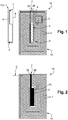
- step 100 (can correspond to step 100 ( fig. 4 ), a first possible step of the method for manufacturing a radiofrequency smart card according to a preferred embodiment is illustrated.
- the card envisaged by the invention is intended to include an insert (or inlay in English).
- this envisaged insert may include a relay antenna (passive or amplifier) which is configured so as to be electromagnetically (or inductively) coupled with a radio frequency module (or transponder).
- a radio frequency module or transponder
- the latter can be inserted into a cavity 3, 3bis of the insert or of the card or positioned at a corresponding location 3.
- the module can be in the form of a tag or RFID tag of fine structure, simply fixed to the card body at location 3 of the module, without being inserted into a cavity.
- the antenna is configured to ensure an inductive coupling or connection with the module, it is not excluded to configure the antenna to have its two ends 2I, (2E, 2D) coming close to the radio frequency module so as to connect in ohmic or capacitive connection.
- its internal end 2I could stop at the edge of the cavity or location 3 of the module.
- its external end 2E or 2F could be brought back with a conductive bridge 6 electrically isolated at the interface with the antenna 2.
- the method can include the step of forming an antenna spiral 12, a cavity 3 (optional but preferred for conventional modules of the smart card type) and a plate capacitor 4 in a metal plate, said spiral comprising an external terminal end and an internal terminal end, at least one forming a first capacitor plate,
- the antenna spiral 12 can be provided in this way or obtained by cutting from a metal plate.
- an antenna pattern 3 (or of a plurality of antenna) is formed in a metal plate in particular by laser cutting.
- Each antenna can be extracted from its metallic base plate, in particular after laminating a covering and / or decoration sheet.
- the plate is here made of steel, but it can be of any known metallic material such as gold, tungsten, silver, aluminum, copper or alloys.
- the cavity 3 can be formed by thinning the thickness of the turns (or thinning the thickness of the metal plate before cutting the turns); It can be obtained by machining or molding in a location 3 indicated by dotted lines on the figure 1 .
- the cavity can be formed by an antenna pattern 2bis which circumvents the location 3 of the cavity.
- the width of the turns is narrower in the area around the cavity.
- the width of the turns can be a few millimeters around the cavity while the turns close to the edge of the card (in particular the outer turn) can be much wider from (0.5 cm or 1 cm) to 2 cm.
- the cavity location 3 includes an opening 3bis passing through the cut metal plate 2.
- the spiral 12 ends at its internal end (terminal end 4) with a metal plate 3 which is obtained in the same way as the antenna turns.
- This plate forms a first capacitor plate which is intended to cooperate with a second capacitor plate 5.
- the method preferably provides for the addition of a second capacitor plate 5 facing at least one of said two end portions 4;
- the second plate extends via an insulated conductive bridge 6 to the other terminal portion 2D, 2E to connect it capacitively or ohmically to form a resonant circuit (RLC).
- RLC resonant circuit
- the method provides for making a PC portion of a conductive metal plate, in particular by cutting from another metal plate.
- the PC portion includes a zone 5 (forming a second capacitor plate) intended to be positioned opposite the first capacitor plate 4. It also includes a zone 6 forming a conductive bridge.
- the entire underside of the PC portion may include an insulator (deposited in particular by material jet, screen printing or other known technique) with the exception of its narrow end 7.
- the second portion PC can be thinned by operation 8 of rectification or milling (or cut from an already thin metal plate before its assembly with the antenna 2).
- a thinning 9 can be provided at the location of the PC portion, indicated in the figure of the second PC portion, can preferably be thinned in particular by milling or the like.
- the assembly of the antenna 2 with the capacitor element PC of the figure 1 is positioned opposite the first plate 4 and connected via its end 7 by electrical welding to an external end 2E of the antenna spiral 12.
- the insulated conductive bridge 6 could be connected, via its end 7, to another adjacent 2D end of the antenna.
- the external coil is sectioned at level "F” on its external transverse side but it could be sectioned at level "D" in the left corner joining the antenna pattern.
- first 4 and second portions 5 of the capacitor plate can be located outside (or at the outer edge) of the spiral 12 (rather than inside the spiral) and be connected capacitively while the end 4 of the central turn is ohmically connected (eg soldering) to one end 5 of the PC plate.
- the PC portion can be placed in the same location, being isolated at the interface with the antenna and forming a capacitive connection.
- the invention according to this preferred embodiment provides for a step 110 intended to keep the turns 2 well spaced from one another.
- the method can provide for the insertion of insulating material between the turns 2 of the antenna spiral 12 in particular by hot or cold lamination (or rolling) or by distributing polymerizable fluid insulating material between the turns.
- This step of holding the turns in place with respect to each other can be carried out before step 120 of adding the capacitor plate PC or after.
- the method may provide for laminating or hot pressing at least one thermoplastic or hot-melt sheet on the antenna.
- the fluidized material flows between the turns and then hardens on cooling.
- the antenna spiral 12 can extend to the edge of the card. This characteristic can be obtained after extraction of the antenna from a large format plate containing a plurality of cut antenna.
- the antenna can be completely embedded in insulating material (for example overmolded).
- the antenna can be extracted from a plate to be deposited inside an insulating frame arranged on an insulating substrate having a larger surface than the antenna then a sheet and / or resin is deposited on the antenna to carry out a lamination.
- each insert can be covered with at least one sheet or insulating covering layer on each main face.
- the antenna can receive in the cavity a radio frequency module (not shown) which conventionally comprises an antenna L1 on an insulating support connected to a radio frequency chip, if necessary, a tuning capacity can be included in the radio frequency chip.
- the module can only be of the contactless type or of the hybrid contact and contactless type. In all preferred cases (in particular for reasons of performance or ease of assembly or connection of the radio frequency module), the module can be inductively coupled with the relay antenna.
- the radio frequency module can be inserted into the cavity 3 before or after the addition of cover and / or finish sheets (from step 130).
- the method performs a rolling of sheets on the insert, the cavity 3 ( fig. 3 ) or the inter turn space may have been filled with resin.
- the method performs cavity machining 3 before inserting the antenna module (not shown).
- the module is thus in coupling position with the insert comprising a relay or passive type antenna (RLC circuit) which provides an extension of the radio frequency communication range of the antenna module (or radio frequency communication transponder).
- the relay antenna R comprises the RLC circuit formed by the spiral 12 (inductance L), and the capacitor 4, 5 (C); Resistance 5 is implicit.
- the antenna spiral can have a thickness of between 300 and 700 ⁇ m.
- the turns can be at least as wide in the plane of the card as high in the direction perpendicular to this plane.
- the turns can be fine in particular around the module (a few hundred microns, or even 1 mm to a few millimeters) and wide at least at the level of the external turn of the order of 0.5 cm from 1 cm.
- the card body plate may comprise an assembly of metal plates welded together or assembled by means of a thin adhesive layer. This last assembly can improve the mechanical resistance of bending / torsion.
- the external turn can have a greater width than the other turns.
- the width can be for example from 0.5 to 1 cm so as to have more mass at the edge.
Abstract
L'invention concerne un procédé de fabrication d'une carte à puce radiofréquence comportant un insert (1A, 1B) avec antenne relais, configurée de manière à être couplée électro-magnétiquement avec un module radiofréquence inséré dans une cavité (3) de la carte,caractérisé en ce que la formation de l'insert comprend les étapes suivantes :- formation d'une spirale d'antenne (12), de ladite cavité (3) et une plaque de condensateur (4) dans une plaque de métal, ladite spirale comportant une extrémité terminale externe (2E, 2F) et une extrémité terminale interne (21), l'une au moins formant ou connectant une première plaque de condensateur (4),- adjonction d'une seconde plaque (5) de condensateur en regard de l'une au moins desdites deux portions terminales de l'antenne (21, 2E, 2F), ladite seconde plaque (5) s'étendant via un pont conducteur isolé (6) jusqu'à l'autre portion terminale (2 E, 2D) pour la connecter de manière capacitive ou ohmique et former un circuit résonant (RLC),- insertion de matière isolante entre les spires (2) de la spirale d'antenne (12).L'invention concerne également un insert pour carte correspondant obtenu notamment par le procédé.The invention relates to a method for manufacturing a radiofrequency smart card comprising an insert (1A, 1B) with relay antenna, configured so as to be electromagnetically coupled with a radiofrequency module inserted in a cavity (3) of the card. , characterized in that the formation of the insert comprises the following stages: - formation of an antenna spiral (12), of said cavity (3) and a capacitor plate (4) in a metal plate, said spiral comprising an external terminal end (2E, 2F) and an internal terminal end (21), at least one forming or connecting a first capacitor plate (4), - adding a second capacitor plate (5) sight of at least one of said two terminal portions of the antenna (21, 2E, 2F), said second plate (5) extending via an insulated conductive bridge (6) to the other terminal portion (2 E, 2D) to connect it capacitively or ohmically and form a resonant circuit (RLC), - inserti there is insulating material between the turns (2) of the antenna spiral (12). The invention also relates to a corresponding card insert obtained in particular by the method.
Description
L'invention concerne le domaine des cartes à puce sans contact comportant un corps de carte à forte teneur métallique ou appelée communément carte métallique (ou métal).The invention relates to the field of contactless smart cards comprising a card body with a high metallic content or commonly called metallic (or metal) card.
Elle vise en particulier et de préférence un procédé de fabrication d'une carte à puce de communication radiofréquence, comportant un insert comprenant une antenne relais (antenne passive, amplificatrice ou booster) configurée de manière à être couplée électro-magnétiquement avec un module radiofréquence inséré dans une cavité de la carte. A la limite, l'invention peut envisager une antenne normale non relais.It relates in particular and preferably to a method of manufacturing a radiofrequency communication smart card, comprising an insert comprising a relay antenna (passive antenna, amplifier or booster) configured so as to be electro-magnetically coupled with an inserted radio frequency module. in a card cavity. Ultimately, the invention can envisage a normal non-relay antenna.
Les cartes à puce peuvent être du type hybride (contacts et sans-contact) ou purement sans-contact (sans bornier de contacts électriques).Smart cards can be of the hybrid type (contacts and contactless) or purely contactless (without electrical contact terminal block).
Les cartes à puce peuvent avoir un module de carte à puce comportant sur un substrat isolant, un transpondeur radiofréquence avec la puce et l'antenne. Les modules de carte à puce radiofréquence sont généralement encartés dans une cavité du corps de carte.Smart cards can have a smart card module comprising on an insulating substrate, a radio frequency transponder with the chip and the antenna. The radio frequency chip card modules are generally inserted in a cavity of the card body.
L'invention vise plus particulièrement les cartes bancaires comportant un corps majoritairement métallique en volume et/ou en masse.The invention relates more particularly to bank cards comprising a mainly metallic body by volume and / or by mass.
On connait un procédé de réalisation d'un insert (ou inlay en anglais) comprenant une antenne en forme de spirale découpée dans une feuille de métal et présentant ses deux extrémités terminales d'interconnexion disposées respectivement à l'intérieur et à l'extérieur des spires. Une résine isolante est coulée sur l'antenne, à l'exception des portions terminales d'interconnexion, de manière à remplir l'espace inter-spires et pour former une cavité de réception d'un module à puce électronique sans contact. Un module est inséré dans la cavité pour interconnecter de manière ohmique les portions terminales d'interconnexion.There is a known method of producing an insert (or inlay in English) comprising a spiral-shaped antenna cut out from a metal sheet and having its two terminal interconnection ends disposed respectively inside and outside the turns. An insulating resin is poured onto the antenna, with the exception of the terminal interconnection portions, so as to fill the inter-turn space and to form a receiving cavity of a contactless electronic chip module. A module is inserted into the cavity to ohmically interconnect the terminal interconnection portions.
Le brevet
Le brevet
Par ailleurs, on connait également des dispositifs radiofréquences hybrides, tels que des cartes à contacts et sans-contact, comportant un module de carte à puce à contacts incorporé dans un corps de carte et connecté à une antenne logée dans le corps de carte.Furthermore, hybrid radio frequency devices are also known, such as contact and contactless cards, comprising a smart card module with contacts incorporated in a card body and connected to an antenna housed in the card body.
Par ailleurs, il existe des cartes bancaires comportant des éléments métalliques en insert à l'intérieur le corps de carte en matière plastique ou en surface externe du corps de carte tel de l'aluminium, du titane, de l'or. Le métal procure une sensation de lourdeur de la carte qui est très appréciée par les utilisateurs. Il donne aussi un aspect esthétique visible qui en fait un produit haut de gamme pour privilégiés.In addition, there are bank cards with metallic elements inserted inside the body of plastic card or external surface of the card body such as aluminum, titanium, gold. The metal provides a feeling of heaviness of the card which is very appreciated by the users. It also gives a visible aesthetic appearance which makes it a high-end product for the privileged.
La demande internationale
La demande de brevet
Il y a donc actuellement une forte demande pour ce genre de carte à puce à forte teneur de métal.There is therefore currently a high demand for this type of smart card with a high metal content.
L'invention vise à résoudre les inconvénients précités.The invention aims to solve the aforementioned drawbacks.
L'invention consiste selon un aspect préféré à avoir des cartes à puce métalliques les plus lourdes possibles avec du métal tout en ayant de bonnes performances radiofréquences.The invention consists in a preferred aspect of having the heaviest metal chip cards possible with metal while having good radio frequency performance.
En particulier, l'invention vise une structure de module à puce électronique pour carte à puce qui permette d'avoir de de bonnes performances radiofréquences dans deux directions au moins (perpendiculaires au plan principal de la carte), même si la carte contient un maximum de métal qui généralement fait écran aux champs électromagnétiques d'un lecteur sans-contact.In particular, the invention relates to an electronic chip module structure for a smart card which makes it possible to have good radio frequency performance in two directions. at least (perpendicular to the main plane of the card), even if the card contains a maximum of metal which generally shields the electromagnetic fields from a contactless reader.
La carte peut de préférence avoir également une structure satisfaisant notamment les contraintes de tenue mécanique du standard ISO des cartes à puce et autres tests de durabilité dans le temps. De telles cartes peuvent être conformes notamment au standard ISO 78016 et/ ou ISO / IEC 14443 ou équivalents.The card may preferably also have a structure satisfying in particular the mechanical strength constraints of the ISO standard for smart cards and other tests of durability over time. Such cards can comply in particular with standard ISO 78016 and / or ISO / IEC 14443 or equivalent.
L'invention vise à résoudre les inconvénients ou à satisfaire objectifs précités. Elle vise de préférence à avoir de bonnes performances radiofréquences avec une carte ayant du métal pouvant s'étendre ou non jusqu'aux bords de la carte.The invention aims to solve the drawbacks or to satisfy the above-mentioned objectives. It preferably aims to have good radio frequency performance with a card having metal which may or may not extend to the edges of the card.
L'invention peut consister à former une antenne relais dans l'épaisseur même d'une plaque métallique avec une épaisseur pouvant être supérieure à 200 ou 300 µm.The invention may consist in forming a relay antenna in the very thickness of a metal plate with a thickness which may be greater than 200 or 300 μm.
A cet effet, l'invention a pour objet un procédé de fabrication d'une carte à puce radiofréquence comportant un insert avec antenne relais configurée de manière à être couplée électro-magnétiquement avec un module radiofréquence inséré dans une cavité de la carte,
caractérisé en ce que la formation de l'insert comprend les étapes suivantes :
- formation d'une spirale d'antenne, de ladite cavité et une plaque de condensateur dans une plaque de métal, ladite spirale comportant une extrémité terminale externe et une extrémité terminale interne, l'une au moins formant une première plaque de condensateur,
- adjonction d'une seconde plaque de condensateur en regard de l'une au moins desdites deux portions terminales et s'étendant via un pont conducteur isolé jusqu'à l'autre portion terminale pour la connecter de manière capacitive ou ohmique pour former un circuit résonant (RLC),
- insertion de matière isolante entre les spires de la spirale d'antenne.
characterized in that the formation of the insert comprises the following stages:
- forming an antenna spiral, said cavity and a capacitor plate in a metal plate, said spiral comprising an external terminal end and an internal terminal end, at least one forming a first capacitor plate,
- adding a second capacitor plate facing at least one of said two end portions and extending via an insulated conductive bridge to the other end portion to connect it capacitively or ohmically to form a resonant circuit (RLC),
- insertion of insulating material between the turns of the antenna spiral.
Grâce à l'invention, l'insert peut comprendre une masse métallique importante au niveau de l'antenne même puisqu'elle est formée dans l'épaisseur d'une plaque de métal pouvant avoir sensiblement ou presque l'épaisseur d'une carte à puce standard.Thanks to the invention, the insert can comprise a large metallic mass at the level of the antenna itself since it is formed in the thickness of a metal plate which may have substantially or almost the thickness of a card to standard chip.
La connexion du module radiofréquence avec l'antenne est facilitée puisqu'il est fait recours d'une antenne relais. Le module est juste fixé à la carte notamment par adhésif sans connexion ohmique (ou soudure) avec l'antenne relais.The connection of the radio frequency module with the antenna is facilitated since it uses a relay antenna. The module is just fixed to the card, in particular by adhesive without ohmic connection (or soldering) with the relay antenna.
Selon d'autres caractéristiques :
- La spirale d'antenne peut s'étendre de préférence jusqu'au bord de la carte ;
- L'insert peut être est recouvert d'au moins une feuille ou couche isolante de recouvrement sur chaque face principale ;
- Le module peut comprendre une antenne sur un support isolant connecté à une puce radiofréquence ;
- La spirale d'antenne peut avoir une épaisseur comprise entre 400 et 700 µm ;
- La cavité peut être formée notamment par formation des pistes ou spires et/ou amincissement de la largeur des pistes ou spires autour de la cavité ;
- La cavité peut être formée en partie dans l'épaisseur de la plaque et/ou quelques spires ;
- Les spires d'antenne peuvent être formées par découpe mécanique, poinçonnage, découpe laser, moulage de matériaux conducteurs.
- The antenna spiral can preferably extend to the edge of the card;
- The insert can be covered with at least one insulating sheet or covering layer on each main face;
- The module can include an antenna on an insulating support connected to a radio frequency chip;
- The antenna spiral can have a thickness of between 400 and 700 μm;
- The cavity can be formed in particular by forming tracks or turns and / or thinning the width of the tracks or turns around the cavity;
- The cavity can be formed partly in the thickness of the plate and / or a few turns;
- The antenna turns can be formed by mechanical cutting, punching, laser cutting, molding of conductive materials.
L'invention a également pour objet une carte à puce radiofréquence comprenant un insert (de carte à puce) comportant de préférence une antenne relais configurée de manière à être couplée électro-magnétiquement avec un module radiofréquence inséré dans une cavité de la carte, caractérisée en ce que l'insert comprend:
- une spirale d'antenne d'épaisseur (pouvant être comprise notamment entre 300 et 700 µm), ladite cavité et une plaque de condensateur, ladite spirale comportant une extrémité terminale externe et une extrémité terminale interne, l'une extrémité au moins formant ou connectant une première plaque de condensateur,
- une seconde plaque de condensateur ajoutée en regard de l'une au moins desdites deux portions terminales de l'antenne, ladite seconde plaque s'étendant via un pont conducteur isolé jusqu'à l'autre portion terminale pour la connecter de manière capacitive ou ohmique et former un circuit résonant (RLC),
- de la matière isolante insérée entre les spires de la spirale d'antenne.
- an antenna spiral of thickness (which may be in particular between 300 and 700 μm), said cavity and a capacitor plate, said spiral comprising an external terminal end and an internal terminal end, the at least one end forming or connecting a first capacitor plate,
- a second capacitor plate added opposite at least one of said two terminal portions of the antenna, said second plate extending via an insulated conductive bridge to the other terminal portion to connect it in a capacitive or ohmic manner and form a resonant circuit (RLC),
- insulating material inserted between the turns of the antenna spiral.
Selon d'autres caractéristiques :
- alternativement, (selon un mode moins préféré) l'antenne de l'insert peut configurée pour être connectée autrement (connexion ohmique, capacitive à un module radiofréquence) ;
- La spirale d'antenne peut s'étendre jusqu'au bord de la carte ;
- La spirale d'antenne ou la première plaque de condensateur peut être amincie localement au niveau de l'emplacement de la seconde plaque de condensateur, notamment pour éviter une surépaisseur localement de l'antenne relais ; Ainsi, le reste de l'antenne relais peut avoir une épaisseur avoisinant celle (0,76 mm) d'une carte à puce standard ISO 7816 et conserver un maximum de masse.
- L'insert peut être recouvert d'au moins une feuille ou couche isolante de recouvrement ou de décoration sur chacune de ses faces principales pour former un corps de carte.
- La spirale d'antenne relais peut présenter des spires ayant une section carrée ou rectangulaire obtenue par découpe laser, ou poinçonnage.
- alternatively, (according to a less preferred mode) the antenna of the insert can be configured to be connected otherwise (ohmic, capacitive connection to a radio frequency module);
- The antenna spiral can extend to the edge of the card;
- The antenna spiral or the first capacitor plate can be thinned locally at the location of the second capacitor plate, in particular to avoid an excess thickness locally of the relay antenna; So the rest of the relay antenna can have a thickness close to that (0.76 mm) of a standard ISO 7816 smart card and keep a maximum of mass.
- The insert can be covered with at least one insulating cover or decoration sheet or layer on each of its main faces to form a card body.
- The relay antenna spiral may have turns having a square or rectangular section obtained by laser cutting, or punching.
-
La
figure 1 illustre une étape de fabrication d'un insert pour carte radiofréquence conformément au mode préféré de l'invention ;Thefigure 1 illustrates a step of manufacturing an insert for a radio frequency card in accordance with the preferred mode of the invention; -
La
figure 2 illustre une étape subséquente d'assemblage comprise dans la fabrication de l'insert pour carte radiofréquence, conformément au mode préféré de l'invention ;Thefigure 2 illustrates a subsequent assembly step included in the manufacture of the insert for radio frequency card, in accordance with the preferred embodiment of the invention; -
La
figure 3 illustre une variante de réalisation de la cavité 3bis dans l'antenne relais, au cours du procédé de fabrication d'un insert pour carte radiofréquence;Thefigure 3 illustrates an alternative embodiment of the cavity 3bis in the relay antenna, during the process of manufacturing an insert for a radiofrequency card; -
La
figure 4 illustre des étapes possibles d'un procédé de fabrication d'un insert à antenne relais pour carte radiofréquence.Thefigure 4 illustrates possible steps in a process for manufacturing a relay antenna insert for a radio frequency card.
A la
On rappelle que la carte envisagée par l'invention est destinée à comporter un insert (ou inlay en anglais). Cet insert envisagé peut comprendre selon l'invention une antenne relais (passive ou amplificatrice) qui est configurée de manière à être couplée électro-magnétiquement (ou inductivement) avec un module (ou transpondeur) radiofréquence. Ce dernier peut être inséré dans une cavité 3, 3bis de l'insert ou de la carte ou positionné à un emplacement correspondant 3.
Par exemple, le module peut être sous forme de tag ou étiquette RFID de structure fine simplement fixé sur le corps de carte à l'emplacement 3 du module, sans être encarté dans une cavité.It will be recalled that the card envisaged by the invention is intended to include an insert (or inlay in English). According to the invention, this envisaged insert may include a relay antenna (passive or amplifier) which is configured so as to be electromagnetically (or inductively) coupled with a radio frequency module (or transponder). The latter can be inserted into a
For example, the module can be in the form of a tag or RFID tag of fine structure, simply fixed to the card body at
Bien que l'antenne soit configurée pour assurer un couplage ou connexion inductif avec le module, il n'est pas exclu de configurer l'antenne pour avoir ses deux extrémités 2I, (2E, 2D) parvenant proche du module radiofréquence de manière à le connecter en connexion ohmique ou capacitive. Par exemple, son extrémité interne 2I pourrait s'arrêter au bord de la cavité ou emplacement 3 de module. Et son extrémité externe 2E ou 2F pourrait être ramenée avec un pont conducteur 6 isolé électriquement à l'interface avec l'antenne 2.Although the antenna is configured to ensure an inductive coupling or connection with the module, it is not excluded to configure the antenna to have its two ends 2I, (2E, 2D) coming close to the radio frequency module so as to connect in ohmic or capacitive connection. For example, its internal end 2I could stop at the edge of the cavity or
Selon une caractéristique de ce mode préféré, le procédé peut comprendre l'étape de formation d'une spirale d'antenne 12, d'une cavité 3 (facultative mais préférée pour des modules classiques type carte à puce) et d'une plaque de condensateur 4 dans une plaque de métal, ladite spirale comportant une extrémité terminale externe et une extrémité terminale interne, l'une au moins formant une première plaque de condensateur,According to a characteristic of this preferred mode, the method can include the step of forming an
La spirale d'antenne 12 peut être fournie ainsi ou obtenue par une découpe dans une plaque de métal. Dans l'exemple (
Alternativement, elle peut être formée par poinçonnage ou par moulage. La plaque est ici en acier, mais elle peut être de toute matière métallique connue telles que de l'or, du tungstène, de l'argent, de l'aluminium, du cuivre ou alliages.Alternatively, it can be formed by punching or by molding. The plate is here made of steel, but it can be of any known metallic material such as gold, tungsten, silver, aluminum, copper or alloys.
La cavité 3 peut être formée par amincissement de l'épaisseur des spires (ou amincissement de l'épaisseur de la plaque de métal avant de découpe des spires) ; Elle peut être obtenue par usinage ou moulage dans un emplacement 3 indiqué en pointillé sur la
Alternativement, (
Ici, il y a une formation des pistes ou spires 2 sans amincissement de la largeur des pistes ou spires autour de la cavité. L'emplacement de cavité 3 comprend une ouverture 3bis traversant la plaque de métal découpée 2.Here, there is a formation of tracks or turns 2 without narrowing the width of the tracks or turns around the cavity. The
Concernant la plaque de condensateur 4 reliée à l'antenne, dans l'exemple (
Selon une caractéristique, le procédé prévoit, de préférence, une adjonction d'une seconde plaque de condensateur 5 en regard de l'une au moins desdites deux portions terminales 4 ; La seconde plaque s'étend via un pont conducteur isolé 6 jusqu'à l'autre portion terminale 2D, 2E pour la connecter de manière capacitive ou ohmique pour former un circuit résonant (RLC).According to one characteristic, the method preferably provides for the addition of a
Dans l'exemple
La seconde portion PC peut être amincie par opération 8 de rectification ou fraisage (ou découpée dans une plaque de métal déjà mince avant son assemblage avec l'antenne 2).The second portion PC can be thinned by
De même, un amincissement 9 peut être prévu à l'emplacement de la portion PC, indiquée sur la figure de la seconde portion PC peut être de préférence amincie notamment par fraisage ou autre.Similarly, a thinning 9 can be provided at the location of the PC portion, indicated in the figure of the second PC portion, can preferably be thinned in particular by milling or the like.
Ainsi, lors de l'assemblage des deux plaques de condensateur, il n'y a pas de surépaisseur au niveau du condensateur, ni du pont conducteur reliant l'extrémité externe de spirale à la seconde plaque de condensateur 5.Thus, during the assembly of the two capacitor plates, there is no additional thickness at the level of the capacitor, nor of the conductive bridge connecting the external end of the spiral to the
Dans les figures, des mêmes références d'une figure à une autre représentent des éléments identiques ou similaires.In the figures, the same references from one figure to another represent identical or similar elements.
A la
La seconde portion PC de plaque de condensateur est positionnée en regard de la première plaque 4 et connectée via son extrémité 7 par soudure électrique à une extrémité externe 2E de la spirale d'antenne 12. Alternativement, le pont conducteur isolé 6 pourrait être connecté, via son extrémité 7, à une autre extrémité adjacente 2D de l'antenne.
La spire externe est sectionnée au niveau « F » sur son côté transversal externe mais elle pourrait être sectionnée au niveau « D » dans l'angle gauche rejoignant le motif d'antenne.To the
The second portion PC of the capacitor plate is positioned opposite the
The external coil is sectioned at level "F" on its external transverse side but it could be sectioned at level "D" in the left corner joining the antenna pattern.
Inversement, les première 4 et seconde portions 5 de plaque de condensateur peuvent se trouver à l'extérieur (ou en bordure externe) de la spirale 12 (plutôt qu'à l'intérieur de la spirale) et être connectée de manière capacitive tandis que l'extrémité 4 de la spire centrale est connectée de manière ohmique (ex. soudure) à une extrémité 5 de la plaque PC.Conversely, the first 4 and
Alternativement, la portion PC peut être posée au même emplacement en étant isolée à l'interface avec l'antenne et former une connexion capacitive.Alternatively, the PC portion can be placed in the same location, being isolated at the interface with the antenna and forming a capacitive connection.
Selon une caractéristique, l'invention selon ce mode préféré prévoit une étape 110 destiné à maintenir les spires 2 bien espacées les unes des autres. A cet, effet, le procédé peut prévoir une insertion de matière isolante entre les spires 2 de la spirale d'antenne 12 notamment par une lamination (ou laminage) à chaud ou à froid ou par distribution de matière isolante fluide polymérisable entre les spires.According to one characteristic, the invention according to this preferred embodiment provides for a
Cette étape de maintien des spires en place les unes par rapport aux autres, peut être réalisée avant l'étape 120 d'adjonction de la plaque de condensateur PC ou après.This step of holding the turns in place with respect to each other, can be carried out before
Alternativement, le procédé peut prévoir de laminer ou presser à chaud au moins une feuille thermoplastique ou thermofusible sur l'antenne. La matière fluidifiée s'écoule entre les spires puis durcit en refroidissant.Alternatively, the method may provide for laminating or hot pressing at least one thermoplastic or hot-melt sheet on the antenna. The fluidized material flows between the turns and then hardens on cooling.
D'une manière générale dans tous les exemples, la spirale d'antenne 12 peut s'étendre jusqu'au bord de la carte. Cette caractéristique peut être obtenue après extraction de l'antenne d'une plaque grand format contenant une pluralité d'antenne découpée.In general in all the examples, the
Alternativement, l'antenne peut se trouver noyée complètement dans de la matière isolante (par exemple surmoulée).Alternatively, the antenna can be completely embedded in insulating material (for example overmolded).
L'antenne peut être extraite d'une plaque pour être déposée à l'intérieur d'un cadre isolant agencé sur un substrat isolant ayant une surface plus grande que l'antenne puis une feuille et/ou de la résine est déposée sur l'antenne pour effectuer une lamination.The antenna can be extracted from a plate to be deposited inside an insulating frame arranged on an insulating substrate having a larger surface than the antenna then a sheet and / or resin is deposited on the antenna to carry out a lamination.
Ainsi chaque insert peut être recouvert d'au moins une feuille ou couche isolante de recouvrement sur chaque face principale.Thus each insert can be covered with at least one sheet or insulating covering layer on each main face.
Une fois la cavité 3 réalisée, L'antenne peut recevoir dans la cavité un module radiofréquence (non représentée) qui comprend de manière classique une antenne L1 sur un support isolant connecté à une puce radiofréquence, le cas échéant, une capacité d'accord peut être incluse dans la puce radiofréquence. Le module peut être uniquement de type sans-contact ou de type hybride contacts et sans-contact. Dans tous les cas préférés (notamment pour des raisons de performance ou de facilité d'assemblage ou de connexion du module radiofréquence), le module peut être couplé inductivement avec l'antenne relais.Once the
Le module radiofréquence peut être inséré dans la cavité 3 avant ou après l'adjonction de feuilles de couverture et/ou de finition (de l'étape 130).
Dans l'exemple
In the example
Dans tous les exemples, la spirale d'antenne peut avoir une épaisseur comprise entre 300 et 700 µm.In all the examples, the antenna spiral can have a thickness of between 300 and 700 μm.
Les spires peuvent être au moins aussi larges dans le plan de la carte que hautes dans le sens perpendiculaire à ce plan. De préférence, les spires peuvent être fines notamment autour du module (quelques centaines de microns, voire 1 mm à quelques millimètres) et larges au moins au niveau de la spire externe de l'ordre de 0,5 cm du 1 cm.The turns can be at least as wide in the plane of the card as high in the direction perpendicular to this plane. Preferably, the turns can be fine in particular around the module (a few hundred microns, or even 1 mm to a few millimeters) and wide at least at the level of the external turn of the order of 0.5 cm from 1 cm.
Dans tous les exemples également, la plaque du corps de carte peut comprendre un assemblage de plaques métalliques soudées ensemble ou assemblées par l'intermédiaire d'une couche fine adhésive. Ce dernier assemblage peut améliorer la tenue mécanique de flexion / torsion.In all of the examples also, the card body plate may comprise an assembly of metal plates welded together or assembled by means of a thin adhesive layer. This last assembly can improve the mechanical resistance of bending / torsion.
De même, la spire externe peut avoir une largeur plus importante que les autres spires. La largeur peut être par exemple de 0,5 à 1 cm de manière à présenter plus de masse en bordure.Likewise, the external turn can have a greater width than the other turns. The width can be for example from 0.5 to 1 cm so as to have more mass at the edge.
Claims (11)
caractérisé en ce que la formation de l'insert comprend les étapes suivantes :
characterized in that the formation of the insert comprises the following stages:
caractérisée en ce que l'insert comprend:
characterized in that the insert comprises:
Priority Applications (2)
| Application Number | Priority Date | Filing Date | Title |
|---|---|---|---|
| EP18306795.8A EP3671563A1 (en) | 2018-12-21 | 2018-12-21 | Method for manufacturing a metal smart card, preferably with relay antenna |
| PCT/EP2019/084087 WO2020126572A1 (en) | 2018-12-21 | 2019-12-06 | Method for manufacturing a metal smart card, preferably with a relay antenna |
Applications Claiming Priority (1)
| Application Number | Priority Date | Filing Date | Title |
|---|---|---|---|
| EP18306795.8A EP3671563A1 (en) | 2018-12-21 | 2018-12-21 | Method for manufacturing a metal smart card, preferably with relay antenna |
Publications (1)
| Publication Number | Publication Date |
|---|---|
| EP3671563A1 true EP3671563A1 (en) | 2020-06-24 |
Family
ID=65228307
Family Applications (1)
| Application Number | Title | Priority Date | Filing Date |
|---|---|---|---|
| EP18306795.8A Withdrawn EP3671563A1 (en) | 2018-12-21 | 2018-12-21 | Method for manufacturing a metal smart card, preferably with relay antenna |
Country Status (2)
| Country | Link |
|---|---|
| EP (1) | EP3671563A1 (en) |
| WO (1) | WO2020126572A1 (en) |
Cited By (1)
| Publication number | Priority date | Publication date | Assignee | Title |
|---|---|---|---|---|
| RU2789826C1 (en) * | 2022-04-28 | 2023-02-10 | Олег Умарович Айбазов | Method for producing cards with metal layer and contactless interface (options) |
Families Citing this family (1)
| Publication number | Priority date | Publication date | Assignee | Title |
|---|---|---|---|---|
| CN112749571B (en) * | 2020-12-28 | 2022-07-05 | 杭州海康威视数字技术股份有限公司 | Card reading terminal and radio frequency identification system |
Citations (7)
| Publication number | Priority date | Publication date | Assignee | Title |
|---|---|---|---|---|
| FR2743649A1 (en) | 1996-01-17 | 1997-07-18 | Gemplus Card Int | CONTACTLESS ELECTRONIC MODULE, ELECTRONIC LABEL CARD INCORPORATING THE SAME, AND METHODS OF MAKING SAME |
| EP1031939B1 (en) | 1997-11-14 | 2005-09-14 | Toppan Printing Co., Ltd. | Composite ic card |
| US20080246664A1 (en) * | 2007-04-06 | 2008-10-09 | Murata Manufacturing Co., Ltd. | Wireless ic device |
| US20150269477A1 (en) | 2012-08-30 | 2015-09-24 | David Finn | Dual-interface hybrid metal smartcard with a booster antenna or coupling frame |
| FR3032294A1 (en) * | 2015-02-02 | 2016-08-05 | Smart Packaging Solutions | CONTACTLESS CHIP CARD WITH DOUBLE ANTENNA |
| EP3182336A1 (en) * | 2015-12-14 | 2017-06-21 | Gemalto Sa | Radiofrequency device with adjustable lc circuit including an electric and/or electronic module |
| WO2018152218A1 (en) | 2017-02-14 | 2018-08-23 | Cpi Card Group - Colorado, Inc. | Edge-to-edge metal card and production method |
-
2018
- 2018-12-21 EP EP18306795.8A patent/EP3671563A1/en not_active Withdrawn
-
2019
- 2019-12-06 WO PCT/EP2019/084087 patent/WO2020126572A1/en active Application Filing
Patent Citations (7)
| Publication number | Priority date | Publication date | Assignee | Title |
|---|---|---|---|---|
| FR2743649A1 (en) | 1996-01-17 | 1997-07-18 | Gemplus Card Int | CONTACTLESS ELECTRONIC MODULE, ELECTRONIC LABEL CARD INCORPORATING THE SAME, AND METHODS OF MAKING SAME |
| EP1031939B1 (en) | 1997-11-14 | 2005-09-14 | Toppan Printing Co., Ltd. | Composite ic card |
| US20080246664A1 (en) * | 2007-04-06 | 2008-10-09 | Murata Manufacturing Co., Ltd. | Wireless ic device |
| US20150269477A1 (en) | 2012-08-30 | 2015-09-24 | David Finn | Dual-interface hybrid metal smartcard with a booster antenna or coupling frame |
| FR3032294A1 (en) * | 2015-02-02 | 2016-08-05 | Smart Packaging Solutions | CONTACTLESS CHIP CARD WITH DOUBLE ANTENNA |
| EP3182336A1 (en) * | 2015-12-14 | 2017-06-21 | Gemalto Sa | Radiofrequency device with adjustable lc circuit including an electric and/or electronic module |
| WO2018152218A1 (en) | 2017-02-14 | 2018-08-23 | Cpi Card Group - Colorado, Inc. | Edge-to-edge metal card and production method |
Cited By (1)
| Publication number | Priority date | Publication date | Assignee | Title |
|---|---|---|---|---|
| RU2789826C1 (en) * | 2022-04-28 | 2023-02-10 | Олег Умарович Айбазов | Method for producing cards with metal layer and contactless interface (options) |
Also Published As
| Publication number | Publication date |
|---|---|
| WO2020126572A1 (en) | 2020-06-25 |
Similar Documents
| Publication | Publication Date | Title |
|---|---|---|
| EP0671705B1 (en) | Manufacturing process for a hybrid card | |
| EP0916144B1 (en) | Method for making a transponder coil | |
| FR2721733A1 (en) | Method for manufacturing a contactless card by overmolding and contactless card obtained by such a method. | |
| EP1428258B1 (en) | Method for making a thin electronic tag | |
| EP1141887B1 (en) | Method for making a contactless chip card | |
| EP3005244B1 (en) | Method for manufacturing an anti-cracking electronic device | |
| EP1190377B1 (en) | Method for the production of a portable integrated circuit electronic device comprising a low-cost dielectric | |
| WO2020126573A1 (en) | Method for producing a radiofrequency chip card insert comprising a metal plate | |
| EP3671563A1 (en) | Method for manufacturing a metal smart card, preferably with relay antenna | |
| EP3899792B1 (en) | Method for manufacturing a metal radiofrequency smart card with improved electromagnetic permittivity | |
| CA2293460A1 (en) | Method for making a contactless smart card | |
| WO2002001495A1 (en) | Hybrid card with ohmic contact and delocalized sinks | |
| FR2905494A1 (en) | ELECTRONIC DEVICE WITH INTEGRATED CIRCUIT MODULE AND ANTENNA CONNECTED BY CAPACITIVE ELECTRICAL CONNECTIONS | |
| WO2020114753A1 (en) | Method for manufacturing a metal or non-metal chip card with relay antenna | |
| WO2021233869A1 (en) | Method for electrochemical metallisation of a double-sided electrical circuit for a smart card and electrical circuit produced using said method | |
| EP4070241A1 (en) | Method for manufacturing a radio frequency smart card comprising a metal plate with a slot in the plate | |
| EP0969410B1 (en) | Chip card comprising an antenna | |
| WO2020099279A1 (en) | Method for producing an electronic insert for a portable multi-component support and insert obtained | |
| WO2020127109A1 (en) | Method for producing a metal radio-frequency smart card having improved permittivity with extended perforations | |
| WO2021048148A1 (en) | Method for manufacturing a metal chip card with mini relay antenna | |
| EP3663984A1 (en) | Method for manufacturing a smart card with interconnection of modules | |
| EP3427190B1 (en) | Method for manufacturing a module with an integrated circuit chip and device comprising such a module | |
| WO2001004988A1 (en) | Antenna for contactless cards, hybrid cards and electronic labels | |
| FR2736453A1 (en) | Fabrication of card accepting integrated circuit to make smart card - by making step-shaped connector strips distributed round edge of hole in card, with circuit placed between and connected by wires | |
| FR3030087A1 (en) | MODULE FOR MICROCIRCUIT CARDS, MICROCIRCUIT CARDS COMPRISING SUCH A MODULE AND METHOD OF MANUFACTURE |
Legal Events
| Date | Code | Title | Description |
|---|---|---|---|
| PUAI | Public reference made under article 153(3) epc to a published international application that has entered the european phase |
Free format text: ORIGINAL CODE: 0009012 |
|
| STAA | Information on the status of an ep patent application or granted ep patent |
Free format text: STATUS: THE APPLICATION HAS BEEN PUBLISHED |
|
| AK | Designated contracting states |
Kind code of ref document: A1 Designated state(s): AL AT BE BG CH CY CZ DE DK EE ES FI FR GB GR HR HU IE IS IT LI LT LU LV MC MK MT NL NO PL PT RO RS SE SI SK SM TR |
|
| AX | Request for extension of the european patent |
Extension state: BA ME |
|
| STAA | Information on the status of an ep patent application or granted ep patent |
Free format text: STATUS: THE APPLICATION IS DEEMED TO BE WITHDRAWN |
|
| 18D | Application deemed to be withdrawn |
Effective date: 20210112 |