EP3340010B1 - Printing apparatus and method for controlling the same - Google Patents
Printing apparatus and method for controlling the same Download PDFInfo
- Publication number
- EP3340010B1 EP3340010B1 EP17209009.4A EP17209009A EP3340010B1 EP 3340010 B1 EP3340010 B1 EP 3340010B1 EP 17209009 A EP17209009 A EP 17209009A EP 3340010 B1 EP3340010 B1 EP 3340010B1
- Authority
- EP
- European Patent Office
- Prior art keywords
- printing apparatus
- power supply
- control means
- image processing
- processing apparatus
- Prior art date
- Legal status (The legal status is an assumption and is not a legal conclusion. Google has not performed a legal analysis and makes no representation as to the accuracy of the status listed.)
- Active
Links
- 238000000034 method Methods 0.000 title claims description 153
- 230000006870 function Effects 0.000 description 12
- 230000004044 response Effects 0.000 description 8
- 238000004891 communication Methods 0.000 description 7
- 238000010586 diagram Methods 0.000 description 3
- 230000005540 biological transmission Effects 0.000 description 1
- 238000001514 detection method Methods 0.000 description 1
- 230000003287 optical effect Effects 0.000 description 1
- 239000007787 solid Substances 0.000 description 1
- 230000003068 static effect Effects 0.000 description 1
- 230000007704 transition Effects 0.000 description 1
Images
Classifications
-
- H—ELECTRICITY
- H04—ELECTRIC COMMUNICATION TECHNIQUE
- H04N—PICTORIAL COMMUNICATION, e.g. TELEVISION
- H04N1/00—Scanning, transmission or reproduction of documents or the like, e.g. facsimile transmission; Details thereof
- H04N1/00885—Power supply means, e.g. arrangements for the control of power supply to the apparatus or components thereof
- H04N1/00888—Control thereof
- H04N1/00896—Control thereof using a low-power mode, e.g. standby
-
- H—ELECTRICITY
- H04—ELECTRIC COMMUNICATION TECHNIQUE
- H04N—PICTORIAL COMMUNICATION, e.g. TELEVISION
- H04N1/00—Scanning, transmission or reproduction of documents or the like, e.g. facsimile transmission; Details thereof
- H04N1/00885—Power supply means, e.g. arrangements for the control of power supply to the apparatus or components thereof
- H04N1/00888—Control thereof
- H04N1/00891—Switching on or off, e.g. for saving power when not in use
-
- G—PHYSICS
- G06—COMPUTING; CALCULATING OR COUNTING
- G06F—ELECTRIC DIGITAL DATA PROCESSING
- G06F1/00—Details not covered by groups G06F3/00 - G06F13/00 and G06F21/00
- G06F1/26—Power supply means, e.g. regulation thereof
- G06F1/266—Arrangements to supply power to external peripherals either directly from the computer or under computer control, e.g. supply of power through the communication port, computer controlled power-strips
-
- G—PHYSICS
- G06—COMPUTING; CALCULATING OR COUNTING
- G06F—ELECTRIC DIGITAL DATA PROCESSING
- G06F1/00—Details not covered by groups G06F3/00 - G06F13/00 and G06F21/00
- G06F1/26—Power supply means, e.g. regulation thereof
- G06F1/32—Means for saving power
- G06F1/3203—Power management, i.e. event-based initiation of a power-saving mode
- G06F1/3234—Power saving characterised by the action undertaken
- G06F1/325—Power saving in peripheral device
- G06F1/3284—Power saving in printer
-
- G—PHYSICS
- G06—COMPUTING; CALCULATING OR COUNTING
- G06F—ELECTRIC DIGITAL DATA PROCESSING
- G06F13/00—Interconnection of, or transfer of information or other signals between, memories, input/output devices or central processing units
- G06F13/14—Handling requests for interconnection or transfer
- G06F13/20—Handling requests for interconnection or transfer for access to input/output bus
- G06F13/24—Handling requests for interconnection or transfer for access to input/output bus using interrupt
-
- H—ELECTRICITY
- H04—ELECTRIC COMMUNICATION TECHNIQUE
- H04N—PICTORIAL COMMUNICATION, e.g. TELEVISION
- H04N1/00—Scanning, transmission or reproduction of documents or the like, e.g. facsimile transmission; Details thereof
- H04N1/00885—Power supply means, e.g. arrangements for the control of power supply to the apparatus or components thereof
- H04N1/00907—Details of supply connection, e.g. arrangement of power cables
-
- H—ELECTRICITY
- H04—ELECTRIC COMMUNICATION TECHNIQUE
- H04N—PICTORIAL COMMUNICATION, e.g. TELEVISION
- H04N2201/00—Indexing scheme relating to scanning, transmission or reproduction of documents or the like, and to details thereof
- H04N2201/0077—Types of the still picture apparatus
- H04N2201/0082—Image hardcopy reproducer
-
- Y—GENERAL TAGGING OF NEW TECHNOLOGICAL DEVELOPMENTS; GENERAL TAGGING OF CROSS-SECTIONAL TECHNOLOGIES SPANNING OVER SEVERAL SECTIONS OF THE IPC; TECHNICAL SUBJECTS COVERED BY FORMER USPC CROSS-REFERENCE ART COLLECTIONS [XRACs] AND DIGESTS
- Y02—TECHNOLOGIES OR APPLICATIONS FOR MITIGATION OR ADAPTATION AGAINST CLIMATE CHANGE
- Y02D—CLIMATE CHANGE MITIGATION TECHNOLOGIES IN INFORMATION AND COMMUNICATION TECHNOLOGIES [ICT], I.E. INFORMATION AND COMMUNICATION TECHNOLOGIES AIMING AT THE REDUCTION OF THEIR OWN ENERGY USE
- Y02D10/00—Energy efficient computing, e.g. low power processors, power management or thermal management
Definitions
- a nonvolatile memory 115 is a non-rewritable nonvolatile storage medium.
- a static random access memory (SRAM), an electrically-erasable programmable read only memory (EEPROM), or the like is used as the nonvolatile memory.
- the image processing apparatus 1 When a predetermined period of time has elapsed after end of a job or when a predetermined period of time has elapsed after a latest input received by the input unit 113, the image processing apparatus 1 is switched to the power saving state. Specifically, the RTC 114 manages an elapsed time after a latest job is executed and a period of time after a latest input is received. When a period of time measured by the RTC 114 reaches a predetermined period of time, the normal state of the image processing apparatus 1 is switched to the power saving state.
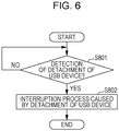
- the image processing apparatus 1 executes an interruption process to be performed when the VBUS is disconnected after stopping the power supply to the VBUS 202.
- the process to be performed when the VBUS is disconnected corresponds to a process to be executed when the USB device 206 is detached.
- the process to be executed when the USB device 206 is detached will be described below with reference to Fig. 6 .
- the CPU 101 executes the suspending process.
- the CPU 101 determines whether the USB device 206 has been attached (S701).
- the four signal lines that is, the VBUS 202, the signal line D-203, the signal line D+ 204, and the GND 205, are connected to the image processing apparatus 1. Thereafter, electric power is supplied from the image processing apparatus 1 to the USB device 206 through the VBUS 202.
- the USB host controller 107 recognizes the USB device 206 and the CPU 101 determines that a USB device is connected.
- the CPU 101 determines whether the USB device 206 has been detached (S801). When the USB device 206 is detached from the image processing apparatus 1, the VBUS 202, the signal line D- 203, the signal line D+ 204, and the GND 205 are not connected. Since the signal lines are brought to a non-connection state, transmission and reception of a signal may not be performed between the image processing apparatus 1 and the USB device 206.
- the USB host controller 107 detects the detachment of the USB device 206 and transmits a notification indicating the detachment of the USB device 206 to the CPU 101. When receiving the notification, the CPU 101 determines that the USB device 206 has been detached from the image processing apparatus 1.
- Fig. 3 is a flowchart of a process performed when the normal state of the image processing apparatus 1 is switched to the power saving state.
- the process in Fig. 3 is realized when the CPU 101 executes a program stored in the HDD 103 or the like.
- the CPU 101 determines whether the interruption process is completed (S306). When the determination is negative, the CPU 101 repeatedly performs the process in step S305 and step S306.
- the CPLD 109 When receiving the suspending completion signal from the CPU 101, the CPLD 109 stops power supply to the second blocks 121, 122, and 123 (S309).
- Fig. 4 is a flowchart of a process performed when the power saving state of the image processing apparatus 1 is switched to the normal state.
- the process in Fig. 4 is realized when the CPU 101 executes a program stored in the HDD 103 or the like.
- the process illustrated in Fig. 4 is started when the CPU 101 receives the restoration signal from the CPLD 109.
- the CPLD 109 restarts the power supply to the second blocks 121, 122, and 123 in which the power supply thereto is stopped in step S308 of Fig. 3 .
Landscapes
- Engineering & Computer Science (AREA)
- Theoretical Computer Science (AREA)
- General Engineering & Computer Science (AREA)
- Multimedia (AREA)
- Signal Processing (AREA)
- Physics & Mathematics (AREA)
- General Physics & Mathematics (AREA)
- Computer Hardware Design (AREA)
- Facsimiles In General (AREA)
- Power Sources (AREA)
- Control Or Security For Electrophotography (AREA)
- Accessory Devices And Overall Control Thereof (AREA)
Description
- The present invention relates to a printing apparatus connected to a device detachable by a user.
- Printing apparatuses which enter a power saving state of low power consumption from a normal state when an operation is not performed for a predetermined period of time are widely used. Before such a printing apparatus enters the power saving state, a suspending process of storing setting values of devices included in the printing apparatus in a memory is performed. Subsequently, power consumption is reduced in the power saving state by stopping supply of electric power to a number of the devices. Thereafter, before the printing apparatus returns from the power saving state to the normal state, the setting values stored in the memory are read and set to the devices. In this way, the consumed power is reduced in the power saving state and the power saving state is restored to the state as before the power saving state.
- When the printing apparatus executes the suspending process, a device connected to the printing apparatus may request execution of an interruption process having a priority level higher than that of the suspending process. The interruption process is performed when writing to the device connected to the printing apparatus is completed, for example. Here, the printing apparatus stops the suspending process so as to execute the interruption process, and therefore, the state of the printing apparatus may not be changed to the power saving state.
- Japanese Patent Laid-Open No.
2011-8688 - European patent publication No.
EP 2 738 642 A1 discloses a method of sensing connection of a USB device by an image forming apparatus in a power save mode. - A general image processing apparatus may be used with a device, such as a universal serial bus (USB) device attached thereto, which is detachable by a user. When such a device is attached to the image processing apparatus, the image processing apparatus performs an interruption process so as to start communication with the device. On the other hand, when the device is detached from the image processing apparatus, the image processing apparatus executes an interruption process so as to terminate the communication with the device.
- In Japanese Patent Laid-Open No.
2011-8688 - Therefore, while the image processing apparatus executes a suspending process, the interruption process caused by attachment or detachment of the device is preferentially executed if the user attaches the device to or detaches the device from the image processing apparatus. As a result of executing the interruption process, the suspending process is interrupted, and the image processing apparatus does not enter the power saving state.
- The present invention provides a process of preventing the interruption process from being performed when a device is attached or detached to the image processing apparatus by a user during a suspending process and entering a power saving state of the image processing apparatus.
- The present invention in its first aspect provides a printing apparatus as specified in
claims 1 to 12. - The present invention in its second aspect provides a method for controlling a printing apparatus as specified in claims 13 to 18.
- Further features of the present invention will become apparent from the following description of exemplary embodiments with reference to the attached drawings.
-
-
Fig. 1 is a diagram illustrating a hardware configuration of an image processing apparatus. -
Fig. 2 is a diagram illustrating a hardware configuration for controlling power supply to a USB device. -
Fig. 3 is a flowchart of a process performed when the image processing apparatus enters a power saving state. -
Fig. 4 is a flowchart of a process performed when the image processing apparatus is restored to a normal state. -
Fig. 5 is a flowchart of a process performed when the USB device is attached to the image processing apparatus in the normal state. -
Fig. 6 is a flowchart of a process performed when the USB device is detached from the image processing apparatus in the normal state. - Hereinafter, preferred embodiments of the present invention will be described with reference to the accompanying drawings. Note that the embodiments below do not limit the present invention associated with the scope of the claims below, and it is not necessarily the case that all combinations of characteristics described in the embodiments are required for solving problems of the present invention.
-
Fig. 1 is a diagram illustrating a hardware configuration of animage processing apparatus 1. The configuration of theimage processing apparatus 1 will be described with reference toFig. 1 . - A central processing unit (CPU) 101 is a central processing arithmetic apparatus which operates software for operating the
image processing apparatus 1. Asystem bus 102 is a path used when theCPU 101 accesses other units or when the other units transmit and receive information with one another. - A hard disk unit (HDD) 103 operates as a storage region which stores the software of the
image processing apparatus 1 and databases and files required for operating theimage processing apparatus 1. Although the HDD is used as the storage region, in this embodiment, a large-capacity nonvolatile memory, such as a solid state drive (SSD), may be used. A random access memory (RAM) 104 is a memory having a region in which a program of theimage processing apparatus 1 is developed. Furthermore, theRAM 104 operates as a storage region which stores variables used for operating programs and data to be transferred from the units by dynamic memory access (DMA). - A
network controller 105 is used when theimage processing apparatus 1 performs communication with other devices on a network. A network controller interface (I/F) 106 is used to connect thenetwork controller 105 with the network. - A
USB host controller 107 controls communication between theimage processing apparatus 1 and a USB device. A USB host I/F 108 is used for connection between theUSB host controller 107 and an external USB device. TheUSB host controller 107 performs device control for controlling aUSB device 206. Although only oneUSB host controller 107 is illustrated inFig. 1 , a plurality ofUSB host controllers 107 may be provided. Theimage processing apparatus 1 and an external USB device are connected to each other through the USB host I/F 108 and a USB cable, not illustrated. The USB device may be directly connected to theimage processing apparatus 1 without using the USB cable depending on a form of the USB device. - A
display unit 111 is a display device which displays an operation state of theimage processing apparatus 1 so that the user can check the operation state. Adisplay unit controller 110 performs display control of thedisplay unit 111. - An
input unit 113 is an input device which receives an instruction issued by the user to theimage processing apparatus 1. Aninput unit controller 112 controls theinput unit 113. Theinput unit 113 is an input device including a keyboard, a mouse, a numeric keypad, a cursor key, a touch panel, and an operation unit keyboard. Furthermore, in a case where theinput unit 113 is a touch panel, the touch panel is overlapped with a surface of thedisplay unit 111, and the touch panel and thedisplay unit 111 are integrated. - A real time clock (RTC) 114 has a clock function, an alarm function, a timer function, and the like of the
image processing apparatus 1. - A
nonvolatile memory 115 is a non-rewritable nonvolatile storage medium. A static random access memory (SRAM), an electrically-erasable programmable read only memory (EEPROM), or the like is used as the nonvolatile memory. - A complex programmable logic device (CPLD) 109 is a program-rewritable logic device. The
CPLD 109 executes a process when theCPU 101 reads a low (0)/high (1) state of a signal line on a base circuit or changes a setting of the low (0)/high (1) state. In this embodiment, the CPLD 109 enables control of ON/OFF of electric power of theimage processing apparatus 1. A general-purpose input/output (GPIO) is included in theCPLD 109. When theCPU 101 changes a setting value of a register of the GPIO, ON/OFF of power supply to various blocks in theimage processing apparatus 1 is enabled. - The
image processing apparatus 1 is connected to ascanner 117 through a scanner I/F 116. Thescanner 117 operates as a reading unit. Furthermore, theimage processing apparatus 1 is connected to aprinter 119 through thesystem bus 102 and a printer I/F 118. Theprinter 119 functions as a printing unit. - The
image processing apparatus 1 includes a first block which constantly maintains an energized state after power is on and second blocks which are not energized when a power saving state is entered. TheCPLD 109 controls an energized state of the first and second blocks. The first block is surrounded by a dottedline 124 inFig. 1 and constantly energized after power is on. On the other hand, the second blocks are surrounded by dottedlines CPU 101 transmits asignal 120 which notifies theCPLD 109 of completion of the suspending process. When receiving thesignal 120 indicating the completion of the suspending process, theCPLD 109 performs a process of stopping power supply to thesecond blocks -
Fig. 2 is a circuit configuration which realizes control of power supply to a USB device connected to theimage processing apparatus 1. - The
USB device 206 communicates with theUSB host controller 107 through four signal lines. AVBUS 202 is a power line used when theimage processing apparatus 1 supplies electric power to theUSB device 206. A signal line D- 203 and asignal line D+ 204 are used to supply data between theUSB device 206 and theUSB host controller 107. AGND 205 indicates a ground signal line. - An AND
circuit 201 controls output by obtaining a logical AND of an output of the GPIO of theCPLD 109 and an output of the VBUS of the USB host I/F 108. In a case where the output of the ANDcircuit 201 is 1, theimage processing apparatus 1 supplies electric power to theUSB device 206, and otherwise, the power supply is not performed. In this embodiment, a state in which an output of the GPIO of theCPLD 109 is changed from 1 to 0 and an output of the ANDcircuit 201 is 0 irrespective of an output of the USB host I/F 108 is referred to as "disconnection of the VBUS". On the other hand, a state in which an output of the GPIO of theCPLD 109 is changed from 0 to 1 and an output of theVBUS 202 when theUSB device 206 is attached to theimage processing apparatus 1 is 1 is referred to as "connection of the VBUS". - In this embodiment, an output of the VBUS of the
USB device 206 is controlled using the ANDcircuit 201. However, an output of theVBUS 202 of theUSB device 206 may be controlled using another general logic circuit. For example, an output of theVBUS 202 may be controlled using a high-side switch and an OR circuit. - Here, a flow of transition from the normal state to the power saving state of the
image processing apparatus 1 of this embodiment will be described with reference toFig. 2 . - When a predetermined period of time has elapsed after end of a job or when a predetermined period of time has elapsed after a latest input received by the
input unit 113, theimage processing apparatus 1 is switched to the power saving state. Specifically, theRTC 114 manages an elapsed time after a latest job is executed and a period of time after a latest input is received. When a period of time measured by theRTC 114 reaches a predetermined period of time, the normal state of theimage processing apparatus 1 is switched to the power saving state. - When the normal state of the
image processing apparatus 1 is switched to the power saving state, theCPU 101 changes an output of the GPIO of theCPLD 109 from 1 to 0. In this case, the ANDcircuit 201 outputs 0 irrespective of an output of the USB host I/F 108. By this, power supply to theVBUS 202 is stopped and the communication between theimage processing apparatus 1 and theUSB device 206 is stopped. - In a case where the
USB device 206 is not connected to theimage processing apparatus 1, after power supply to the VBUS is stopped, theimage processing apparatus 1 executes the suspending process without performing an interruption process to be performed in response to detachment of theUSB device 206. The suspending process includes a process of storing setting values of various devices controlled by corresponding device drivers and setting values indicating states of the drivers in a nonvolatile memory. - If the
USB device 206 is connected to theimage processing apparatus 1, theimage processing apparatus 1 executes an interruption process to be performed when the VBUS is disconnected after stopping the power supply to theVBUS 202. The process to be performed when the VBUS is disconnected corresponds to a process to be executed when theUSB device 206 is detached. The process to be executed when theUSB device 206 is detached will be described below with reference toFig. 6 . After the interruption process performed in response to the disconnection of theVBUS 202 is completed, theCPU 101 executes the suspending process. - In this embodiment, the
image processing apparatus 1 stops power supply to theVBUS 202, executes the interruption process that is performed when theUSB device 206 is detached, and performs the suspending process. By this, even if the user attaches or detaches theUSB device 206 while the suspending process is executed, the interruption process is not executed. - First, the interruption process performed when the
USB device 206 is attached to theimage processing apparatus 1 and the interruption process performed when theUSB device 206 is detached will be described with reference toFigs. 5 and6 . -
Fig. 5 is a flowchart of the interruption process performed when theUSB device 206 is attached to theimage processing apparatus 1. A program for executing the process of this flowchart is stored in theHDD 103 of theimage processing apparatus 1, and the process is realized when theCPU 101 executes the program. - The
CPU 101 determines whether theUSB device 206 has been attached (S701). When theUSB device 206 is attached to theimage processing apparatus 1, the four signal lines, that is, theVBUS 202, the signal line D-203, thesignal line D+ 204, and theGND 205, are connected to theimage processing apparatus 1. Thereafter, electric power is supplied from theimage processing apparatus 1 to theUSB device 206 through theVBUS 202. When the electric power is supplied to theUSB device 206 and differential signals of the signal line D- 203 and thesignal line D+ 204 are operated, theUSB host controller 107 recognizes theUSB device 206 and theCPU 101 determines that a USB device is connected. - The
CPU 101 receives a request for performing the interruption process in response to the attachment of theUSB device 206 from theUSB host controller 107 and executes the interruption process (S702). TheCPU 101 communicates with theUSB device 206 so as to execute an enumeration process for analyzing a specification and a configuration of theUSB device 206. Here, theCPU 101 requests theUSB device 206 to transmit a descriptor indicating the specification, such as a type or a function, of theUSB device 206. TheCPU 101 may determine a function of theconnected USB device 206 by analyzing the received descriptor. TheCPU 101 associates theUSB device 206 with a device driver corresponding to theUSB device 206 based on information obtained by the analysis and stores a result of the association in theRAM 104. - The
CPU 101 executes a process of realizing the function of the connected USB device 206 (S703). In step S702, for example, if theconnected USB device 206 is in a storage class and functions as a storage device, a process for enabling access to theUSB device 206 is performed through a storage class driver. By performing this process, theUSB device 206 may be mounted on theimage processing apparatus 1 and access to folders and data in theconnected USB device 206 is enabled through a file system. Furthermore, in step S702, if theconnected USB device 206 is an input type, such as a USB card reader, a notification indicating the connection of the card reader is transmitted to application software and a process for performing reading/writing of data from the card reader is executed. -
Fig. 6 is a flowchart of the process performed when theUSB device 206 is detached from theimage processing apparatus 1. A program for executing the process of the flowchart ofFig. 6 is stored in theHDD 103 of theimage processing apparatus 1, and the process is realized when theCPU 101 executes the program. - The
CPU 101 determines whether theUSB device 206 has been detached (S801). When theUSB device 206 is detached from theimage processing apparatus 1, theVBUS 202, the signal line D- 203, thesignal line D+ 204, and theGND 205 are not connected. Since the signal lines are brought to a non-connection state, transmission and reception of a signal may not be performed between theimage processing apparatus 1 and theUSB device 206. TheUSB host controller 107 detects the detachment of theUSB device 206 and transmits a notification indicating the detachment of theUSB device 206 to theCPU 101. When receiving the notification, theCPU 101 determines that theUSB device 206 has been detached from theimage processing apparatus 1. - In step S801, when it is determined that the
USB device 206 has not been detached, theCPU 101 executes the process of step S801 again. - In step S801, when it is determined that the
USB device 206 has been detached, theCPU 101 executes the interruption process to be performed when theUSB device 206 is detached (S802). Here, theCPU 101 cancels the association between theUSB device 206 and the device driver performed in step S702. Since the association between theUSB device 206 and the device driver is cancelled, any application may not access theUSB device 206. - In
Fig. 6 , a process performed after theUSB device 206 is detached from theimage processing apparatus 1 is described. In a case where theUSB device 206 attached to theimage processing apparatus 1 is a storage device, if theUSB device 206 is detached from theimage processing apparatus 1 in a state in which theUSB device 206 is mounted on theimage processing apparatus 1, the file system in theimage processing apparatus 1 may be destroyed. Therefore, before theUSB device 206 is detached from theimage processing apparatus 1, a process of stopping access from theimage processing apparatus 1 to theUSB device 206 is required to be performed. - The process of stopping access from the
image processing apparatus 1 to theUSB device 206 is started when an instruction for starting the process is received from the user. The user inputs an instruction for performing unmounting using a screen displayed in thedisplay unit 111 and theinput unit 113 so that access from theimage processing apparatus 1 to theUSB device 206 is stopped. When receiving the input, theCPU 101 unmounts the file system mounted in step S702. By performing this process, the storage device may be detached from theimage processing apparatus 1 without destroying the file system. -
Fig. 3 is a flowchart of a process performed when the normal state of theimage processing apparatus 1 is switched to the power saving state. The process inFig. 3 is realized when theCPU 101 executes a program stored in theHDD 103 or the like. - The
CPU 101 starts the process of the flowchart inFig. 3 when theRTC 114 detects that a predetermined period of time has elapsed after a latest job is terminated or that a predetermined period of time has elapsed after a latest input to theinput unit 113 is performed. - The
CPU 101 determines whether theimage processing apparatus 1 may enter the power saving state (S301). Here, theCPU 101 makes an inquiry indicating whether various software modules including a software module controlling theprinter 119 and a software module controlling thescanner 117 which operate in theimage processing apparatus 1 may enter the power saving state. A state in which such a software module may not enter the power saving state corresponds to a case where the software module is executing another process, for example. Theimage processing apparatus 1 proceeds to step S302 when all the modules which receive the inquiry may enter the power saving state. If at least one of the software modules may not enter the power saving state, theCPU 101 determines that theimage processing apparatus 1 may not enter the power saving state and terminates the process inFig. 3 . - When the determination is affirmative in step S301, the
CPU 101 requests the software module which controls theUSB host controller 107 to perform a process of stopping access to the USB device 206 (S302). When receiving a signal from theCPU 101, the software module which controls theUSB host controller 107 executes the process of stopping the access to theUSB device 206 connected to theimage processing apparatus 1. If a USB storage is connected to theimage processing apparatus 1, the mounting is cancelled so that access by theCPU 101 to the USB storage through the file system is prohibited. Furthermore, if a USB device, such as a USB card reader is connected, an instruction for stopping execution of a process of reading information from the USB card reader and writing information to the USB card reader is issued to application software which executes the process. - After the process of access to the
USB device 206 is stopped in step S302, theCPU 101 disconnects the VBUS 202 (S303). TheCPU 101 operates the register of the GPIO included in theCPLD 109 so as to cause a signal line which connects theCPLD 109 with the ANDcircuit 201 to output 0. TheCPLD 109 outputs a signal of 0 even though theUSB host controller 107 is in operation and the output is 1, and therefore, an output of theVBUS 202 corresponding to an output from the ANDcircuit 201 is 0. When theVBUS 202 outputs 0, even if theUSB device 206 is physically connected to theimage processing apparatus 1, theUSB device 206 is electrically disconnected from theimage processing apparatus 1. - The
CPU 101 determines whether the interruption process to be performed in response to the disconnection of theVBUS 202 has been detected (S304). In step S303, in a case where theUSB device 206 is connected while theVBUS 202 is disconnected, theimage processing apparatus 1 and theUSB device 206 are electrically disconnected and an interruption signal which requests the interruption process for terminating the communication is generated. On the other hand, in step S303, in a case where theUSB device 206 is not connected when the VBUS is disconnected, the interruption signal is not generated even if theVBUS 202 is disconnected. When the interruption signal is not detected until a predetermined period of time has elapsed, theCPU 101 proceeds to step S307 described below. - When the interruption signal is detected in step S304, the
CPU 101 executes the interruption process to be performed in response to the disconnection of the VBUS (S305). The process executed in step S305 is the same as the interruption process to be performed when theUSB device 206 is detached from theimage processing apparatus 1. - The
CPU 101 determines whether the interruption process is completed (S306). When the determination is negative, theCPU 101 repeatedly performs the process in step S305 and step S306. - After the interruption process is terminated, the
CPU 101 performs the suspending process of the device drivers of the general-purpose OS (S307). In step S307, theCPU 101 performs a process of storing register information of hardware which is used by the device drivers in operation and state variables indicating states of the various devices in a nonvolatile memory. - After the suspending process of the device drivers is completed, the
CPU 101 executes the suspending process of a kernel of the general-purpose OS (S308). In step S308, theCPU 101 performs a process of storing register information of hardware which is used by the kernel in operation and a state variable indicating a state of the hardware in the nonvolatile memory. When the device drivers and the kernel enter the suspending state, theCPU 101 outputs a suspending completion signal to theCPLD 109. - When receiving the suspending completion signal from the
CPU 101, theCPLD 109 stops power supply to thesecond blocks -
Fig. 4 is a flowchart of a process performed when the power saving state of theimage processing apparatus 1 is switched to the normal state. The process inFig. 4 is realized when theCPU 101 executes a program stored in theHDD 103 or the like. - The
image processing apparatus 1 starts a process of restoration from the power saving state to the normal state when detecting that a job is input from an external apparatus, such as a PC, connected through a network or when detecting that a predetermined button included in theimage processing apparatus 1 is pressed. Specifically, theCPLD 109 transmits a signal for restoration to theCPU 101 when an input of a job or press of a predetermined button is detected. - The process illustrated in
Fig. 4 is started when theCPU 101 receives the restoration signal from theCPLD 109. TheCPLD 109 restarts the power supply to thesecond blocks Fig. 3 . - When receiving the restoration signal from the
CPLD 109, theCPU 101 performs a resuming process of the kernel and the device drivers of the general-purpose OS (S401). In step S401, theCPU 101 reads the register information of the hardware and the state variables which are stored in step S306 and step S307 ofFig. 3 and performs a process of writing the information and the state variables in the registers of the devices and the like. - After the resuming process of the kernel and the device drivers of the general-purpose OS is completed, the
CPU 101 operates the register of the GPIO included in theCPLD 109 so as to cause theCPLD 109 to output 1 (S402). - In a case where the
USB device 206 is attached to theimage processing apparatus 1, the ANDcircuit 201outputs 1 and electric power is supplied to theUSB device 206. When the electric power is supplied to theVBUS 202 of theUSB device 206, theUSB device 206 and theimage processing apparatus 1 may communicate with each other. In step S402, when theUSB device 206 is not attached to theimage processing apparatus 1, theVBUS 202 continuously outputs 0. - After the
CPU 101 changes a value of the GPIO of theCPLD 109 to 1, theCPU 101 determines whether theUSB device 206 is connected to the image processing apparatus 1 (S403). Here, theCPU 101 detects an interruption signal generated when theUSB device 206 is attached to theimage processing apparatus 1. When detecting the interruption signal, theCPU 101 determines that theUSB device 206 is connected to theimage processing apparatus 1. When the USB device is connected, theCPU 101 performs an interruption process for starting communication with the USB device and proceeds to step S404. When theCPU 101 does not detect an interruption signal, theCPU 101 determines that the USB device is not connected to theimage processing apparatus 1 and terminates the process inFig. 4 . In step S403, the process of determining whether the USB device is attached to theimage processing apparatus 1 is not limited to the process described above. - When it is determined that the
USB device 206 is connected to theimage processing apparatus 1 in step S403, theCPU 101 performs a process of restarting access to the USB device 206 (S404). When theUSB device 206 is a USB storage, a mounting process is executed so that theCPU 101 may access the USB storage through the file system. Furthermore, when an input-type USB device, such as a USB card reader, is connected, a notification indicating connection of the card reader is transmitted to application software so that a writing process and a reading process may be performed on the USB card reader. - After the process in step S404 is executed, the
image processing apparatus 1 terminates the process in the flowchart ofFig. 4 . - By executing the process described above, an interruption process to be performed when the user performs attachment or detachment of a device, such as a USB device, is prevented from being performed during the suspending process of the
image processing apparatus 1. Accordingly, theimage processing apparatus 1 may perform power control so that the normal state is switched to the power saving state. - Furthermore, termination of the interruption process performed in response to the disconnection of the
VBUS 202 is detected after theVBUS 202 is disconnected, and thereafter, the suspending process is executed on a device corresponding to a device driver of theimage processing apparatus 1. Accordingly, a case where theimage processing apparatus 1 is prevented from entering the power saving state because the interruption process in response to disconnection of theVBUS 202 and the suspending process are simultaneously performed is prevented from occurring. - In the first embodiment, it is determined whether an interruption signal has generated in response to disconnection of the
VBUS 202 in step S304 ofFig. 3 . When an interruption signal is detected, the process in step S305 and step S306 is executed. However, instead of the detection of an interruption signal performed in step S304, it is determined whether a USB device is connected before a VBUS is disconnected. - The
CPU 101 recognizes that theUSB device 206 is attached to theimage processing apparatus 1 and stores information indicating that theUSB device 206 is attached to theimage processing apparatus 1 in theRAM 104. When theCPU 101 determines that theUSB device 206 is connected before the disconnection of the VBUS with reference to the information stored in theRAM 104, the process in step S305 and step S306 is executed. On the other hand, if a USB device is not connected to theimage processing apparatus 1 before disconnection of the VBUS, a process from S307 onwards is executed. - The present invention is applicable to interfaces other than a USB including FIREWIRE (registered trademark). Other Embodiments
- Embodiment(s) of the present invention can also be realized by a computer of a system or apparatus that reads out and executes computer executable instructions (e.g., one or more programs) recorded on a storage medium (which may also be referred to more fully as a 'non-transitory computer-readable storage medium') to perform the functions of one or more of the above-described embodiment(s) and/or that includes one or more circuits (e.g., application specific integrated circuit (ASIC)) for performing the functions of one or more of the above-described embodiment(s), and by a method performed by the computer of the system or apparatus by, for example, reading out and executing the computer executable instructions from the storage medium to perform the functions of one or more of the above-described embodiment(s) and/or controlling the one or more circuits to perform the functions of one or more of the above-described embodiment(s). The computer may comprise one or more processors (e.g., central processing unit (CPU), micro processing unit (MPU)) and may include a network of separate computers or separate processors to read out and execute the computer executable instructions. The computer executable instructions may be provided to the computer, for example, from a network or the storage medium. The storage medium may include, for example, one or more of a hard disk, a random-access memory (RAM), a read only memory (ROM), a storage of distributed computing systems, an optical disk (such as a compact disc (CD), digital versatile disc (DVD), or Blu-ray Disc (BD)™), a flash memory device, a memory card, and the like.
Claims (18)
- A printing apparatus capable of entering a power saving state, the printing apparatus comprising:an interface (108);power supply means (202) configured to supply electric power to a device (206) connected to the interface (108);power control means (109) configured to stop power supply to the device (206); andcontrol means (101) configured to execute, on the printing apparatus, a suspending process of the device (206) in accordance with a request for causing the printing apparatus to enter the power saving state, characterized in thatthe power control means (109) stops power supply to the device (206) after the request is received and before the suspending process of the device (206) is performed.
- The printing apparatus according to claim 1, further comprising:storage means (115),wherein the suspending process of the device (206) at least includes a process of storing a state of a device driver which controls the device (206) in the storage means (115) .
- The printing apparatus according to claim 1, further comprising:storage means (115),wherein the suspending process of the device (206) at least includes a process of storing values set in the device (206) in the storage means (115).
- The printing apparatus according to claim 1,
wherein the control means (101) performs a process of stopping access to the device (206) in accordance with the request, and
the power control means (109) stops power supply to the device (206) after the stopping process is executed and before the suspending process of the device (206) is started. - The printing apparatus according to claim 1,
wherein the control means (101) outputs a predetermined signal to the power control means (109) after completion of the suspending process, and
the power control means (109) stops power supply to the interface (108) in accordance with the predetermined signal. - The printing apparatus according to claim 1, further comprising:display means (111),wherein the control means (101) outputs a predetermined signal to the power control means (109) after the suspending process is completed, andthe power control means (109) stops power supply to the display means (111) in accordance with the predetermined signal.
- The printing apparatus according to claim 1,
wherein the control means (101) executes an interruption process to be performed when power supply to the device (206) is stopped and starts the suspending process after the interruption process is completed. - The printing apparatus according to claim 1,
wherein the interface (108) is a USB interface. - The printing apparatus according to claim 8,
wherein the power control means (109) stops power supply to a VBUS (202) of a USB device (206) connected to the USB interface (108) after the request is received and before the suspending process is started. - The printing apparatus according to claim 1,
wherein the control means (101) executes a resuming process of the device (206) in accordance with a request for restoring the printing apparatus from the power saving state. - The printing apparatus according to claim 1,
wherein the control means (101) executes a suspending process of a kernel after the suspending process of the device (206) is completed. - The printing apparatus according to claim 1, further comprising a logical gate (201) configured to receive a control signal controlled by the power control means (109) and electric power output from the power supply means (202) and to stop output of the electric power in accordance with the control signal.
- A method for controlling a printing apparatus capable of entering a power saving state, the method comprising:supplying electric power to a device (206) connected to an interface of the printing apparatus;receiving a request for causing the printing apparatus to enter a power saving state;stopping power supply to the device (206) connected to the interface; characterized bystarting, on the printing apparatus, execution of a suspending process of the device (206) in accordance with the request after power supply to the device is stopped.
- The method for controlling a printing apparatus according to claim 13, wherein the suspending process of the device (206) includes at least a process of storing a state of a device driver which controls the device in storage means.
- The method for controlling a printing apparatus according to claim 13, wherein the suspending process of the device includes at least a process of storing values set in the device in storage means.
- The method for controlling a printing apparatus according to claim 13, further comprising stopping access to the device before power supply to the device is stopped.
- The method for controlling a printing apparatus according to claim 13, further comprising:executing an interruption process to be performed when power supply to the device is stopped,wherein the suspending process is performed after the interruption process is executed.
- The method for controlling a printing apparatus according to claim 13,
wherein the interface is a USB interface, and the device is a USB device, and
stop of power supply to the device corresponds to stop of power supply to a VBUS of a USB device connected to the USB interface.
Applications Claiming Priority (1)
| Application Number | Priority Date | Filing Date | Title |
|---|---|---|---|
| JP2016249171A JP2018103383A (en) | 2016-12-22 | 2016-12-22 | Image processing device, control method and program of image processing device |
Publications (2)
| Publication Number | Publication Date |
|---|---|
| EP3340010A1 EP3340010A1 (en) | 2018-06-27 |
| EP3340010B1 true EP3340010B1 (en) | 2019-12-18 |
Family
ID=60953565
Family Applications (1)
| Application Number | Title | Priority Date | Filing Date |
|---|---|---|---|
| EP17209009.4A Active EP3340010B1 (en) | 2016-12-22 | 2017-12-20 | Printing apparatus and method for controlling the same |
Country Status (4)
| Country | Link |
|---|---|
| US (1) | US10425545B2 (en) |
| EP (1) | EP3340010B1 (en) |
| JP (1) | JP2018103383A (en) |
| CN (1) | CN108234804B9 (en) |
Family Cites Families (20)
| Publication number | Priority date | Publication date | Assignee | Title |
|---|---|---|---|---|
| JPH11194847A (en) * | 1998-01-06 | 1999-07-21 | Toshiba Corp | Computer system and initialization controller |
| JP2001100875A (en) * | 1999-09-29 | 2001-04-13 | Matsushita Electric Ind Co Ltd | Usb controller |
| US6845457B1 (en) * | 2000-09-26 | 2005-01-18 | Sun Microsystems, Inc. | Method and apparatus for controlling transitions between a first and a second clock frequency |
| JP2004038290A (en) * | 2002-06-28 | 2004-02-05 | Toshiba Corp | Information processing system and disk control method for use in same system |
| US7565561B2 (en) | 2005-05-26 | 2009-07-21 | Canon Kabushiki Kaisha | System for controlling voltage supplied to communication interface between energy-saving mode and normal mode through the used of a resistor upon whether external device is connected |
| JP4361073B2 (en) * | 2005-07-28 | 2009-11-11 | 株式会社リコー | Image processing apparatus and control method thereof |
| JP4843372B2 (en) * | 2006-05-09 | 2011-12-21 | 株式会社リコー | Image processing device |
| US8006166B2 (en) | 2007-06-12 | 2011-08-23 | Micron Technology, Inc. | Programming error correction code into a solid state memory device with varying bits per cell |
| JP5317542B2 (en) * | 2008-06-12 | 2013-10-16 | キヤノン株式会社 | Information processing apparatus, control method, and program |
| JP2011008688A (en) | 2009-06-29 | 2011-01-13 | Toshiba Corp | Control method for built-in system |
| JP2012038156A (en) * | 2010-08-09 | 2012-02-23 | Nec Access Technica Ltd | Network equipment, power saving method of network equipment and its program |
| DE102011088416A1 (en) * | 2010-12-16 | 2012-06-21 | Canon K. K. | INFORMATION PROCESSING DEVICE FOR SUITABLY PERFORMING DOWN PROCESSING, METHOD FOR CONTROLLING THE INFORMATION PROCESSING DEVICE AND STORAGE MEDIUM |
| JP5790007B2 (en) * | 2011-02-09 | 2015-10-07 | 株式会社リコー | Information processing apparatus, information processing apparatus control method, and program |
| JP5811611B2 (en) * | 2011-06-14 | 2015-11-11 | 株式会社リコー | Information processing apparatus, information processing method, and program |
| US8307127B1 (en) * | 2011-07-06 | 2012-11-06 | Oracle International Corporation | Device live suspend and resume |
| US20130031392A1 (en) * | 2011-07-29 | 2013-01-31 | Mclane William J | Usb device side wake-up for power conservation and management |
| JP5848153B2 (en) * | 2012-02-17 | 2016-01-27 | ルネサスエレクトロニクス株式会社 | Signal processing apparatus and semiconductor device |
| JP2013176878A (en) | 2012-02-28 | 2013-09-09 | Canon Inc | Image forming apparatus, control method of image forming apparatus and program |
| KR102044898B1 (en) | 2012-12-03 | 2019-11-14 | 휴렛-팩커드 디벨롭먼트 컴퍼니, 엘.피. | Method for sensing connection of USB device and image forming apparatus performing the same |
| JP2015098096A (en) | 2013-11-18 | 2015-05-28 | キヤノン株式会社 | Image forming device, and control method for image forming device |
-
2016
- 2016-12-22 JP JP2016249171A patent/JP2018103383A/en active Pending
-
2017
- 2017-12-14 US US15/842,622 patent/US10425545B2/en active Active
- 2017-12-20 EP EP17209009.4A patent/EP3340010B1/en active Active
- 2017-12-20 CN CN201711383915.5A patent/CN108234804B9/en active Active
Non-Patent Citations (1)
| Title |
|---|
| None * |
Also Published As
| Publication number | Publication date |
|---|---|
| EP3340010A1 (en) | 2018-06-27 |
| US10425545B2 (en) | 2019-09-24 |
| CN108234804B (en) | 2020-08-25 |
| CN108234804A (en) | 2018-06-29 |
| US20180183962A1 (en) | 2018-06-28 |
| JP2018103383A (en) | 2018-07-05 |
| CN108234804B9 (en) | 2020-10-13 |
Similar Documents
| Publication | Publication Date | Title |
|---|---|---|
| US9778844B2 (en) | Installation of operating system on host computer using virtual storage of BMC | |
| US9158628B2 (en) | Bios failover update with service processor having direct serial peripheral interface (SPI) access | |
| US9529410B2 (en) | Service processor (SP) initiated data transaction with BIOS utilizing power off commands | |
| TWI477970B (en) | Mode switch method of electronic device and assocaited electronic device | |
| US9680712B2 (en) | Hardware management and control of computer components through physical layout diagrams | |
| US9529750B2 (en) | Service processor (SP) initiated data transaction with bios utilizing interrupt | |
| US20180210783A1 (en) | Information processing apparatus, control method of the same, and storage medium | |
| US10075609B2 (en) | Information processing apparatus and control method thereof for reducing transition time from a power-save mode | |
| EP3588355A1 (en) | Information processing apparatus for detecting tampering with software executed at boot time, method for rebooting information processing apparatus, storage medium, and program | |
| US9749189B2 (en) | Generating graphical diagram of physical layout of computer platforms | |
| TWI774145B (en) | Host device and memory system | |
| EP3340010B1 (en) | Printing apparatus and method for controlling the same | |
| KR102550886B1 (en) | System on chip and operating method thereof | |
| CN111508439A (en) | Information processing apparatus, control method of information processing apparatus, and storage medium | |
| US10795423B2 (en) | Electronic apparatus with power saving mode, control method thereof, and storage medium | |
| US11113386B2 (en) | Information processing apparatus, control method for information processing apparatus, and storage medium | |
| CN105446903A (en) | Information processing method and electronic device | |
| US8041846B2 (en) | Apparatus with reduced latency for master and slave storage devices | |
| US11907729B2 (en) | Computer system and booting method thereof | |
| CN110362349B (en) | Virtual input management device and management method thereof | |
| US11474580B2 (en) | Enablement of wake on finger print sensor without USB enumeration | |
| JP4815775B2 (en) | Device driver installation method and installation system | |
| JP2024058152A (en) | Information processing device and method for controlling the information processing device | |
| KR100953268B1 (en) | Usb device for supports an automatic safety remove using capacitance | |
| JPH0668011A (en) | Scsi interface device |
Legal Events
| Date | Code | Title | Description |
|---|---|---|---|
| PUAI | Public reference made under article 153(3) epc to a published international application that has entered the european phase |
Free format text: ORIGINAL CODE: 0009012 |
|
| STAA | Information on the status of an ep patent application or granted ep patent |
Free format text: STATUS: THE APPLICATION HAS BEEN PUBLISHED |
|
| AK | Designated contracting states |
Kind code of ref document: A1 Designated state(s): AL AT BE BG CH CY CZ DE DK EE ES FI FR GB GR HR HU IE IS IT LI LT LU LV MC MK MT NL NO PL PT RO RS SE SI SK SM TR |
|
| AX | Request for extension of the european patent |
Extension state: BA ME |
|
| STAA | Information on the status of an ep patent application or granted ep patent |
Free format text: STATUS: REQUEST FOR EXAMINATION WAS MADE |
|
| 17P | Request for examination filed |
Effective date: 20190102 |
|
| RBV | Designated contracting states (corrected) |
Designated state(s): AL AT BE BG CH CY CZ DE DK EE ES FI FR GB GR HR HU IE IS IT LI LT LU LV MC MK MT NL NO PL PT RO RS SE SI SK SM TR |
|
| GRAP | Despatch of communication of intention to grant a patent |
Free format text: ORIGINAL CODE: EPIDOSNIGR1 |
|
| STAA | Information on the status of an ep patent application or granted ep patent |
Free format text: STATUS: GRANT OF PATENT IS INTENDED |
|
| INTG | Intention to grant announced |
Effective date: 20190705 |
|
| GRAS | Grant fee paid |
Free format text: ORIGINAL CODE: EPIDOSNIGR3 |
|
| GRAA | (expected) grant |
Free format text: ORIGINAL CODE: 0009210 |
|
| STAA | Information on the status of an ep patent application or granted ep patent |
Free format text: STATUS: THE PATENT HAS BEEN GRANTED |
|
| AK | Designated contracting states |
Kind code of ref document: B1 Designated state(s): AL AT BE BG CH CY CZ DE DK EE ES FI FR GB GR HR HU IE IS IT LI LT LU LV MC MK MT NL NO PL PT RO RS SE SI SK SM TR |
|
| REG | Reference to a national code |
Ref country code: CH Ref legal event code: EP |
|
| REG | Reference to a national code |
Ref country code: DE Ref legal event code: R096 Ref document number: 602017009826 Country of ref document: DE |
|
| REG | Reference to a national code |
Ref country code: IE Ref legal event code: FG4D |
|
| REG | Reference to a national code |
Ref country code: AT Ref legal event code: REF Ref document number: 1215314 Country of ref document: AT Kind code of ref document: T Effective date: 20200115 |
|
| REG | Reference to a national code |
Ref country code: NL Ref legal event code: MP Effective date: 20191218 |
|
| PG25 | Lapsed in a contracting state [announced via postgrant information from national office to epo] |
Ref country code: LV Free format text: LAPSE BECAUSE OF FAILURE TO SUBMIT A TRANSLATION OF THE DESCRIPTION OR TO PAY THE FEE WITHIN THE PRESCRIBED TIME-LIMIT Effective date: 20191218 Ref country code: SE Free format text: LAPSE BECAUSE OF FAILURE TO SUBMIT A TRANSLATION OF THE DESCRIPTION OR TO PAY THE FEE WITHIN THE PRESCRIBED TIME-LIMIT Effective date: 20191218 Ref country code: NO Free format text: LAPSE BECAUSE OF FAILURE TO SUBMIT A TRANSLATION OF THE DESCRIPTION OR TO PAY THE FEE WITHIN THE PRESCRIBED TIME-LIMIT Effective date: 20200318 Ref country code: LT Free format text: LAPSE BECAUSE OF FAILURE TO SUBMIT A TRANSLATION OF THE DESCRIPTION OR TO PAY THE FEE WITHIN THE PRESCRIBED TIME-LIMIT Effective date: 20191218 Ref country code: GR Free format text: LAPSE BECAUSE OF FAILURE TO SUBMIT A TRANSLATION OF THE DESCRIPTION OR TO PAY THE FEE WITHIN THE PRESCRIBED TIME-LIMIT Effective date: 20200319 Ref country code: BG Free format text: LAPSE BECAUSE OF FAILURE TO SUBMIT A TRANSLATION OF THE DESCRIPTION OR TO PAY THE FEE WITHIN THE PRESCRIBED TIME-LIMIT Effective date: 20200318 Ref country code: FI Free format text: LAPSE BECAUSE OF FAILURE TO SUBMIT A TRANSLATION OF THE DESCRIPTION OR TO PAY THE FEE WITHIN THE PRESCRIBED TIME-LIMIT Effective date: 20191218 |
|
| REG | Reference to a national code |
Ref country code: LT Ref legal event code: MG4D |
|
| PG25 | Lapsed in a contracting state [announced via postgrant information from national office to epo] |
Ref country code: RS Free format text: LAPSE BECAUSE OF FAILURE TO SUBMIT A TRANSLATION OF THE DESCRIPTION OR TO PAY THE FEE WITHIN THE PRESCRIBED TIME-LIMIT Effective date: 20191218 Ref country code: HR Free format text: LAPSE BECAUSE OF FAILURE TO SUBMIT A TRANSLATION OF THE DESCRIPTION OR TO PAY THE FEE WITHIN THE PRESCRIBED TIME-LIMIT Effective date: 20191218 |
|
| PG25 | Lapsed in a contracting state [announced via postgrant information from national office to epo] |
Ref country code: AL Free format text: LAPSE BECAUSE OF FAILURE TO SUBMIT A TRANSLATION OF THE DESCRIPTION OR TO PAY THE FEE WITHIN THE PRESCRIBED TIME-LIMIT Effective date: 20191218 |
|
| PG25 | Lapsed in a contracting state [announced via postgrant information from national office to epo] |
Ref country code: CZ Free format text: LAPSE BECAUSE OF FAILURE TO SUBMIT A TRANSLATION OF THE DESCRIPTION OR TO PAY THE FEE WITHIN THE PRESCRIBED TIME-LIMIT Effective date: 20191218 Ref country code: PT Free format text: LAPSE BECAUSE OF FAILURE TO SUBMIT A TRANSLATION OF THE DESCRIPTION OR TO PAY THE FEE WITHIN THE PRESCRIBED TIME-LIMIT Effective date: 20200513 Ref country code: EE Free format text: LAPSE BECAUSE OF FAILURE TO SUBMIT A TRANSLATION OF THE DESCRIPTION OR TO PAY THE FEE WITHIN THE PRESCRIBED TIME-LIMIT Effective date: 20191218 Ref country code: RO Free format text: LAPSE BECAUSE OF FAILURE TO SUBMIT A TRANSLATION OF THE DESCRIPTION OR TO PAY THE FEE WITHIN THE PRESCRIBED TIME-LIMIT Effective date: 20191218 Ref country code: NL Free format text: LAPSE BECAUSE OF FAILURE TO SUBMIT A TRANSLATION OF THE DESCRIPTION OR TO PAY THE FEE WITHIN THE PRESCRIBED TIME-LIMIT Effective date: 20191218 |
|
| REG | Reference to a national code |
Ref country code: BE Ref legal event code: MM Effective date: 20191231 |
|
| PG25 | Lapsed in a contracting state [announced via postgrant information from national office to epo] |
Ref country code: SK Free format text: LAPSE BECAUSE OF FAILURE TO SUBMIT A TRANSLATION OF THE DESCRIPTION OR TO PAY THE FEE WITHIN THE PRESCRIBED TIME-LIMIT Effective date: 20191218 Ref country code: IS Free format text: LAPSE BECAUSE OF FAILURE TO SUBMIT A TRANSLATION OF THE DESCRIPTION OR TO PAY THE FEE WITHIN THE PRESCRIBED TIME-LIMIT Effective date: 20200418 Ref country code: SM Free format text: LAPSE BECAUSE OF FAILURE TO SUBMIT A TRANSLATION OF THE DESCRIPTION OR TO PAY THE FEE WITHIN THE PRESCRIBED TIME-LIMIT Effective date: 20191218 |
|
| REG | Reference to a national code |
Ref country code: DE Ref legal event code: R097 Ref document number: 602017009826 Country of ref document: DE |
|
| PG25 | Lapsed in a contracting state [announced via postgrant information from national office to epo] |
Ref country code: MC Free format text: LAPSE BECAUSE OF FAILURE TO SUBMIT A TRANSLATION OF THE DESCRIPTION OR TO PAY THE FEE WITHIN THE PRESCRIBED TIME-LIMIT Effective date: 20191218 |
|
| REG | Reference to a national code |
Ref country code: AT Ref legal event code: MK05 Ref document number: 1215314 Country of ref document: AT Kind code of ref document: T Effective date: 20191218 |
|
| PLBE | No opposition filed within time limit |
Free format text: ORIGINAL CODE: 0009261 |
|
| STAA | Information on the status of an ep patent application or granted ep patent |
Free format text: STATUS: NO OPPOSITION FILED WITHIN TIME LIMIT |
|
| PG25 | Lapsed in a contracting state [announced via postgrant information from national office to epo] |
Ref country code: ES Free format text: LAPSE BECAUSE OF FAILURE TO SUBMIT A TRANSLATION OF THE DESCRIPTION OR TO PAY THE FEE WITHIN THE PRESCRIBED TIME-LIMIT Effective date: 20191218 Ref country code: DK Free format text: LAPSE BECAUSE OF FAILURE TO SUBMIT A TRANSLATION OF THE DESCRIPTION OR TO PAY THE FEE WITHIN THE PRESCRIBED TIME-LIMIT Effective date: 20191218 Ref country code: LU Free format text: LAPSE BECAUSE OF NON-PAYMENT OF DUE FEES Effective date: 20191220 Ref country code: IE Free format text: LAPSE BECAUSE OF NON-PAYMENT OF DUE FEES Effective date: 20191220 |
|
| 26N | No opposition filed |
Effective date: 20200921 |
|
| PG25 | Lapsed in a contracting state [announced via postgrant information from national office to epo] |
Ref country code: BE Free format text: LAPSE BECAUSE OF NON-PAYMENT OF DUE FEES Effective date: 20191231 Ref country code: SI Free format text: LAPSE BECAUSE OF FAILURE TO SUBMIT A TRANSLATION OF THE DESCRIPTION OR TO PAY THE FEE WITHIN THE PRESCRIBED TIME-LIMIT Effective date: 20191218 Ref country code: AT Free format text: LAPSE BECAUSE OF FAILURE TO SUBMIT A TRANSLATION OF THE DESCRIPTION OR TO PAY THE FEE WITHIN THE PRESCRIBED TIME-LIMIT Effective date: 20191218 |
|
| PG25 | Lapsed in a contracting state [announced via postgrant information from national office to epo] |
Ref country code: IT Free format text: LAPSE BECAUSE OF FAILURE TO SUBMIT A TRANSLATION OF THE DESCRIPTION OR TO PAY THE FEE WITHIN THE PRESCRIBED TIME-LIMIT Effective date: 20191218 |
|
| PG25 | Lapsed in a contracting state [announced via postgrant information from national office to epo] |
Ref country code: PL Free format text: LAPSE BECAUSE OF FAILURE TO SUBMIT A TRANSLATION OF THE DESCRIPTION OR TO PAY THE FEE WITHIN THE PRESCRIBED TIME-LIMIT Effective date: 20191218 |
|
| PG25 | Lapsed in a contracting state [announced via postgrant information from national office to epo] |
Ref country code: CY Free format text: LAPSE BECAUSE OF FAILURE TO SUBMIT A TRANSLATION OF THE DESCRIPTION OR TO PAY THE FEE WITHIN THE PRESCRIBED TIME-LIMIT Effective date: 20191218 |
|
| PG25 | Lapsed in a contracting state [announced via postgrant information from national office to epo] |
Ref country code: MT Free format text: LAPSE BECAUSE OF FAILURE TO SUBMIT A TRANSLATION OF THE DESCRIPTION OR TO PAY THE FEE WITHIN THE PRESCRIBED TIME-LIMIT Effective date: 20191218 Ref country code: HU Free format text: LAPSE BECAUSE OF FAILURE TO SUBMIT A TRANSLATION OF THE DESCRIPTION OR TO PAY THE FEE WITHIN THE PRESCRIBED TIME-LIMIT; INVALID AB INITIO Effective date: 20171220 |
|
| REG | Reference to a national code |
Ref country code: CH Ref legal event code: PL |
|
| PG25 | Lapsed in a contracting state [announced via postgrant information from national office to epo] |
Ref country code: CH Free format text: LAPSE BECAUSE OF NON-PAYMENT OF DUE FEES Effective date: 20201231 Ref country code: LI Free format text: LAPSE BECAUSE OF NON-PAYMENT OF DUE FEES Effective date: 20201231 |
|
| PG25 | Lapsed in a contracting state [announced via postgrant information from national office to epo] |
Ref country code: TR Free format text: LAPSE BECAUSE OF FAILURE TO SUBMIT A TRANSLATION OF THE DESCRIPTION OR TO PAY THE FEE WITHIN THE PRESCRIBED TIME-LIMIT Effective date: 20191218 |
|
| PG25 | Lapsed in a contracting state [announced via postgrant information from national office to epo] |
Ref country code: MK Free format text: LAPSE BECAUSE OF FAILURE TO SUBMIT A TRANSLATION OF THE DESCRIPTION OR TO PAY THE FEE WITHIN THE PRESCRIBED TIME-LIMIT Effective date: 20191218 |
|
| PGFP | Annual fee paid to national office [announced via postgrant information from national office to epo] |
Ref country code: GB Payment date: 20231121 Year of fee payment: 7 |
|
| PGFP | Annual fee paid to national office [announced via postgrant information from national office to epo] |
Ref country code: FR Payment date: 20231122 Year of fee payment: 7 Ref country code: DE Payment date: 20231121 Year of fee payment: 7 |