EP3212714B1 - Silicon containing block copolymers for direct self-assembly application - Google Patents
Silicon containing block copolymers for direct self-assembly application Download PDFInfo
- Publication number
- EP3212714B1 EP3212714B1 EP15794100.6A EP15794100A EP3212714B1 EP 3212714 B1 EP3212714 B1 EP 3212714B1 EP 15794100 A EP15794100 A EP 15794100A EP 3212714 B1 EP3212714 B1 EP 3212714B1
- Authority
- EP
- European Patent Office
- Prior art keywords
- block copolymer
- alkyl
- repeat unit
- hydrogen
- substrate
- Prior art date
- Legal status (The legal status is an assumption and is not a legal conclusion. Google has not performed a legal analysis and makes no representation as to the accuracy of the status listed.)
- Active
Links
- 229920001400 block copolymer Polymers 0.000 title claims description 109
- 238000001338 self-assembly Methods 0.000 title claims description 12
- 229910052710 silicon Inorganic materials 0.000 title description 27
- XUIMIQQOPSSXEZ-UHFFFAOYSA-N Silicon Chemical compound [Si] XUIMIQQOPSSXEZ-UHFFFAOYSA-N 0.000 title description 26
- 239000010703 silicon Substances 0.000 title description 26
- 238000000034 method Methods 0.000 claims description 61
- 239000000758 substrate Substances 0.000 claims description 60
- 230000008569 process Effects 0.000 claims description 42
- 125000004435 hydrogen atom Chemical group [H]* 0.000 claims description 36
- 239000000203 mixture Substances 0.000 claims description 35
- 239000001257 hydrogen Substances 0.000 claims description 34
- 229910052739 hydrogen Inorganic materials 0.000 claims description 34
- 125000004178 (C1-C4) alkyl group Chemical group 0.000 claims description 32
- 229920000642 polymer Polymers 0.000 claims description 32
- 239000002904 solvent Substances 0.000 claims description 23
- 238000000137 annealing Methods 0.000 claims description 22
- 238000002408 directed self-assembly Methods 0.000 claims description 21
- 125000002496 methyl group Chemical group [H]C([H])([H])* 0.000 claims description 16
- 238000001020 plasma etching Methods 0.000 claims description 14
- QVGXLLKOCUKJST-UHFFFAOYSA-N atomic oxygen Chemical compound [O] QVGXLLKOCUKJST-UHFFFAOYSA-N 0.000 claims description 11
- 239000001301 oxygen Substances 0.000 claims description 11
- 229910052760 oxygen Inorganic materials 0.000 claims description 11
- 239000011248 coating agent Substances 0.000 claims description 7
- 238000000576 coating method Methods 0.000 claims description 7
- 125000003709 fluoroalkyl group Chemical group 0.000 claims description 7
- 238000000059 patterning Methods 0.000 claims description 5
- 125000000229 (C1-C4)alkoxy group Chemical group 0.000 claims description 4
- IJGRMHOSHXDMSA-UHFFFAOYSA-N Atomic nitrogen Chemical compound N#N IJGRMHOSHXDMSA-UHFFFAOYSA-N 0.000 claims description 4
- 150000004820 halides Chemical class 0.000 claims description 4
- RTZKZFJDLAIYFH-UHFFFAOYSA-N ether Substances CCOCC RTZKZFJDLAIYFH-UHFFFAOYSA-N 0.000 claims description 3
- DNIAPMSPPWPWGF-UHFFFAOYSA-N monopropylene glycol Natural products CC(O)CO DNIAPMSPPWPWGF-UHFFFAOYSA-N 0.000 claims description 3
- 235000013772 propylene glycol Nutrition 0.000 claims description 3
- 238000011161 development Methods 0.000 claims description 2
- 229910052757 nitrogen Inorganic materials 0.000 claims description 2
- 125000005599 alkyl carboxylate group Chemical group 0.000 claims 2
- 239000010410 layer Substances 0.000 description 60
- 229920002120 photoresistant polymer Polymers 0.000 description 50
- 230000007935 neutral effect Effects 0.000 description 40
- OKKJLVBELUTLKV-UHFFFAOYSA-N Methanol Chemical compound OC OKKJLVBELUTLKV-UHFFFAOYSA-N 0.000 description 18
- -1 dimethylsiloxane Chemical class 0.000 description 14
- 239000000126 substance Substances 0.000 description 12
- 239000000243 solution Substances 0.000 description 11
- ARXJGSRGQADJSQ-UHFFFAOYSA-N 1-methoxypropan-2-ol Chemical compound COCC(C)O ARXJGSRGQADJSQ-UHFFFAOYSA-N 0.000 description 10
- PPBRXRYQALVLMV-UHFFFAOYSA-N Styrene Chemical compound C=CC1=CC=CC=C1 PPBRXRYQALVLMV-UHFFFAOYSA-N 0.000 description 10
- 239000000463 material Substances 0.000 description 10
- 238000012545 processing Methods 0.000 description 9
- 125000000217 alkyl group Chemical group 0.000 description 8
- 239000006117 anti-reflective coating Substances 0.000 description 8
- XLYOFNOQVPJJNP-UHFFFAOYSA-N water Substances O XLYOFNOQVPJJNP-UHFFFAOYSA-N 0.000 description 7
- QTBSBXVTEAMEQO-UHFFFAOYSA-N Acetic acid Chemical compound CC(O)=O QTBSBXVTEAMEQO-UHFFFAOYSA-N 0.000 description 6
- OKTJSMMVPCPJKN-UHFFFAOYSA-N Carbon Chemical compound [C] OKTJSMMVPCPJKN-UHFFFAOYSA-N 0.000 description 6
- YXFVVABEGXRONW-UHFFFAOYSA-N Toluene Chemical compound CC1=CC=CC=C1 YXFVVABEGXRONW-UHFFFAOYSA-N 0.000 description 6
- 229910052799 carbon Inorganic materials 0.000 description 6
- LZCLXQDLBQLTDK-UHFFFAOYSA-N ethyl 2-hydroxypropanoate Chemical compound CCOC(=O)C(C)O LZCLXQDLBQLTDK-UHFFFAOYSA-N 0.000 description 6
- 239000010408 film Substances 0.000 description 6
- 238000001459 lithography Methods 0.000 description 6
- VLKZOEOYAKHREP-UHFFFAOYSA-N n-Hexane Chemical compound CCCCCC VLKZOEOYAKHREP-UHFFFAOYSA-N 0.000 description 6
- LLHKCFNBLRBOGN-UHFFFAOYSA-N propylene glycol methyl ether acetate Chemical compound COCC(C)OC(C)=O LLHKCFNBLRBOGN-UHFFFAOYSA-N 0.000 description 6
- 230000005855 radiation Effects 0.000 description 5
- XKRFYHLGVUSROY-UHFFFAOYSA-N Argon Chemical compound [Ar] XKRFYHLGVUSROY-UHFFFAOYSA-N 0.000 description 4
- CURLTUGMZLYLDI-UHFFFAOYSA-N Carbon dioxide Chemical compound O=C=O CURLTUGMZLYLDI-UHFFFAOYSA-N 0.000 description 4
- 239000000654 additive Substances 0.000 description 4
- 238000013459 approach Methods 0.000 description 4
- 229920001577 copolymer Polymers 0.000 description 4
- 125000000753 cycloalkyl group Chemical group 0.000 description 4
- 230000001419 dependent effect Effects 0.000 description 4
- 239000000178 monomer Substances 0.000 description 4
- 239000003960 organic solvent Substances 0.000 description 4
- 238000001039 wet etching Methods 0.000 description 4
- RYHBNJHYFVUHQT-UHFFFAOYSA-N 1,4-Dioxane Chemical compound C1COCCO1 RYHBNJHYFVUHQT-UHFFFAOYSA-N 0.000 description 3
- 239000004793 Polystyrene Substances 0.000 description 3
- RDOXTESZEPMUJZ-UHFFFAOYSA-N anisole Chemical compound COC1=CC=CC=C1 RDOXTESZEPMUJZ-UHFFFAOYSA-N 0.000 description 3
- 238000007796 conventional method Methods 0.000 description 3
- 238000004132 cross linking Methods 0.000 description 3
- 229920000359 diblock copolymer Polymers 0.000 description 3
- 238000000407 epitaxy Methods 0.000 description 3
- 229940116333 ethyl lactate Drugs 0.000 description 3
- 238000001914 filtration Methods 0.000 description 3
- 238000007654 immersion Methods 0.000 description 3
- 229920005573 silicon-containing polymer Polymers 0.000 description 3
- 238000003756 stirring Methods 0.000 description 3
- 238000012546 transfer Methods 0.000 description 3
- YEJRWHAVMIAJKC-UHFFFAOYSA-N 4-Butyrolactone Chemical compound O=C1CCCO1 YEJRWHAVMIAJKC-UHFFFAOYSA-N 0.000 description 2
- UGFAIRIUMAVXCW-UHFFFAOYSA-N Carbon monoxide Chemical compound [O+]#[C-] UGFAIRIUMAVXCW-UHFFFAOYSA-N 0.000 description 2
- PXGOKWXKJXAPGV-UHFFFAOYSA-N Fluorine Chemical compound FF PXGOKWXKJXAPGV-UHFFFAOYSA-N 0.000 description 2
- XPDWGBQVDMORPB-UHFFFAOYSA-N Fluoroform Chemical compound FC(F)F XPDWGBQVDMORPB-UHFFFAOYSA-N 0.000 description 2
- 238000005033 Fourier transform infrared spectroscopy Methods 0.000 description 2
- VVQNEPGJFQJSBK-UHFFFAOYSA-N Methyl methacrylate Chemical compound COC(=O)C(C)=C VVQNEPGJFQJSBK-UHFFFAOYSA-N 0.000 description 2
- VYPSYNLAJGMNEJ-UHFFFAOYSA-N Silicium dioxide Chemical compound O=[Si]=O VYPSYNLAJGMNEJ-UHFFFAOYSA-N 0.000 description 2
- 230000001476 alcoholic effect Effects 0.000 description 2
- 229910052786 argon Inorganic materials 0.000 description 2
- DKPFZGUDAPQIHT-UHFFFAOYSA-N butyl acetate Chemical compound CCCCOC(C)=O DKPFZGUDAPQIHT-UHFFFAOYSA-N 0.000 description 2
- 239000001569 carbon dioxide Substances 0.000 description 2
- 229910002092 carbon dioxide Inorganic materials 0.000 description 2
- 229910002091 carbon monoxide Inorganic materials 0.000 description 2
- HGCIXCUEYOPUTN-UHFFFAOYSA-N cyclohexene Chemical compound C1CCC=CC1 HGCIXCUEYOPUTN-UHFFFAOYSA-N 0.000 description 2
- NNBZCPXTIHJBJL-UHFFFAOYSA-N decalin Chemical compound C1CCCC2CCCCC21 NNBZCPXTIHJBJL-UHFFFAOYSA-N 0.000 description 2
- 238000000151 deposition Methods 0.000 description 2
- 230000008021 deposition Effects 0.000 description 2
- 238000001035 drying Methods 0.000 description 2
- 238000005516 engineering process Methods 0.000 description 2
- 150000002148 esters Chemical class 0.000 description 2
- 238000005530 etching Methods 0.000 description 2
- IIEWJVIFRVWJOD-UHFFFAOYSA-N ethylcyclohexane Chemical compound CCC1CCCCC1 IIEWJVIFRVWJOD-UHFFFAOYSA-N 0.000 description 2
- 229910052731 fluorine Inorganic materials 0.000 description 2
- 239000011737 fluorine Substances 0.000 description 2
- 238000009472 formulation Methods 0.000 description 2
- 230000008570 general process Effects 0.000 description 2
- 229910052736 halogen Inorganic materials 0.000 description 2
- 150000002367 halogens Chemical class 0.000 description 2
- CATSNJVOTSVZJV-UHFFFAOYSA-N heptan-2-one Chemical compound CCCCCC(C)=O CATSNJVOTSVZJV-UHFFFAOYSA-N 0.000 description 2
- 150000002430 hydrocarbons Chemical group 0.000 description 2
- 230000007062 hydrolysis Effects 0.000 description 2
- 238000006460 hydrolysis reaction Methods 0.000 description 2
- XMGQYMWWDOXHJM-UHFFFAOYSA-N limonene Chemical compound CC(=C)C1CCC(C)=CC1 XMGQYMWWDOXHJM-UHFFFAOYSA-N 0.000 description 2
- 238000004519 manufacturing process Methods 0.000 description 2
- UAEPNZWRGJTJPN-UHFFFAOYSA-N methylcyclohexane Chemical compound CC1CCCCC1 UAEPNZWRGJTJPN-UHFFFAOYSA-N 0.000 description 2
- 238000012986 modification Methods 0.000 description 2
- 230000004048 modification Effects 0.000 description 2
- BKIMMITUMNQMOS-UHFFFAOYSA-N nonane Chemical compound CCCCCCCCC BKIMMITUMNQMOS-UHFFFAOYSA-N 0.000 description 2
- 239000011295 pitch Substances 0.000 description 2
- 238000002360 preparation method Methods 0.000 description 2
- 229960004063 propylene glycol Drugs 0.000 description 2
- 239000011541 reaction mixture Substances 0.000 description 2
- 229910052814 silicon oxide Inorganic materials 0.000 description 2
- 238000009987 spinning Methods 0.000 description 2
- 150000003440 styrenes Chemical class 0.000 description 2
- 125000003011 styrenyl group Chemical group [H]\C(*)=C(/[H])C1=C([H])C([H])=C([H])C([H])=C1[H] 0.000 description 2
- 125000001424 substituent group Chemical group 0.000 description 2
- 239000004094 surface-active agent Substances 0.000 description 2
- 125000000999 tert-butyl group Chemical group [H]C([H])([H])C(*)(C([H])([H])[H])C([H])([H])[H] 0.000 description 2
- TXEYQDLBPFQVAA-UHFFFAOYSA-N tetrafluoromethane Chemical compound FC(F)(F)F TXEYQDLBPFQVAA-UHFFFAOYSA-N 0.000 description 2
- 229910052719 titanium Inorganic materials 0.000 description 2
- 239000010936 titanium Substances 0.000 description 2
- 238000012876 topography Methods 0.000 description 2
- BESKSSIEODQWBP-UHFFFAOYSA-N 3-tris(trimethylsilyloxy)silylpropyl 2-methylprop-2-enoate Chemical group CC(=C)C(=O)OCCC[Si](O[Si](C)(C)C)(O[Si](C)(C)C)O[Si](C)(C)C BESKSSIEODQWBP-UHFFFAOYSA-N 0.000 description 1
- 239000004215 Carbon black (E152) Substances 0.000 description 1
- 239000004970 Chain extender Substances 0.000 description 1
- 239000004971 Cross linker Substances 0.000 description 1
- XDTMQSROBMDMFD-UHFFFAOYSA-N Cyclohexane Chemical compound C1CCCCC1 XDTMQSROBMDMFD-UHFFFAOYSA-N 0.000 description 1
- CTQNGGLPUBDAKN-UHFFFAOYSA-N O-Xylene Chemical compound CC1=CC=CC=C1C CTQNGGLPUBDAKN-UHFFFAOYSA-N 0.000 description 1
- 229910052581 Si3N4 Inorganic materials 0.000 description 1
- RTAQQCXQSZGOHL-UHFFFAOYSA-N Titanium Chemical compound [Ti] RTAQQCXQSZGOHL-UHFFFAOYSA-N 0.000 description 1
- 101100107923 Vitis labrusca AMAT gene Proteins 0.000 description 1
- 239000002253 acid Substances 0.000 description 1
- 150000004996 alkyl benzenes Chemical class 0.000 description 1
- HFEHLDPGIKPNKL-UHFFFAOYSA-N allyl iodide Chemical compound ICC=C HFEHLDPGIKPNKL-UHFFFAOYSA-N 0.000 description 1
- 230000004075 alteration Effects 0.000 description 1
- 238000003491 array Methods 0.000 description 1
- 230000008901 benefit Effects 0.000 description 1
- 230000015572 biosynthetic process Effects 0.000 description 1
- 238000012661 block copolymerization Methods 0.000 description 1
- 230000008859 change Effects 0.000 description 1
- 238000006243 chemical reaction Methods 0.000 description 1
- 125000000113 cyclohexyl group Chemical group [H]C1([H])C([H])([H])C([H])([H])C([H])(*)C([H])([H])C1([H])[H] 0.000 description 1
- 125000001511 cyclopentyl group Chemical group [H]C1([H])C([H])([H])C([H])([H])C([H])(*)C1([H])[H] 0.000 description 1
- 125000001559 cyclopropyl group Chemical group [H]C1([H])C([H])([H])C1([H])* 0.000 description 1
- DIOQZVSQGTUSAI-NJFSPNSNSA-N decane Chemical compound CCCCCCCCC[14CH3] DIOQZVSQGTUSAI-NJFSPNSNSA-N 0.000 description 1
- 238000000276 deep-ultraviolet lithography Methods 0.000 description 1
- WNAHIZMDSQCWRP-UHFFFAOYSA-N dodecane-1-thiol Chemical compound CCCCCCCCCCCCS WNAHIZMDSQCWRP-UHFFFAOYSA-N 0.000 description 1
- 230000000694 effects Effects 0.000 description 1
- 238000000609 electron-beam lithography Methods 0.000 description 1
- 230000002708 enhancing effect Effects 0.000 description 1
- QPADNTZLUBYNEN-UHFFFAOYSA-N etallobarbital Chemical compound C=CCC1(CC)C(=O)NC(=O)NC1=O QPADNTZLUBYNEN-UHFFFAOYSA-N 0.000 description 1
- 150000002170 ethers Chemical class 0.000 description 1
- 125000001495 ethyl group Chemical group [H]C([H])([H])C([H])([H])* 0.000 description 1
- 238000001900 extreme ultraviolet lithography Methods 0.000 description 1
- 239000000706 filtrate Substances 0.000 description 1
- 239000007789 gas Substances 0.000 description 1
- 229910052732 germanium Inorganic materials 0.000 description 1
- 229930195733 hydrocarbon Natural products 0.000 description 1
- 125000002887 hydroxy group Chemical group [H]O* 0.000 description 1
- 125000002768 hydroxyalkyl group Chemical group 0.000 description 1
- 238000003384 imaging method Methods 0.000 description 1
- 238000000671 immersion lithography Methods 0.000 description 1
- 230000010354 integration Effects 0.000 description 1
- 125000001449 isopropyl group Chemical group [H]C([H])([H])C([H])(*)C([H])([H])[H] 0.000 description 1
- 150000002596 lactones Chemical class 0.000 description 1
- 229940087305 limonene Drugs 0.000 description 1
- 235000001510 limonene Nutrition 0.000 description 1
- 238000010551 living anionic polymerization reaction Methods 0.000 description 1
- 229920002521 macromolecule Polymers 0.000 description 1
- 238000003760 magnetic stirring Methods 0.000 description 1
- UZKWTJUDCOPSNM-UHFFFAOYSA-N methoxybenzene Substances CCCCOC=C UZKWTJUDCOPSNM-UHFFFAOYSA-N 0.000 description 1
- GYNNXHKOJHMOHS-UHFFFAOYSA-N methyl-cycloheptane Natural products CC1CCCCCC1 GYNNXHKOJHMOHS-UHFFFAOYSA-N 0.000 description 1
- 238000004377 microelectronic Methods 0.000 description 1
- DIOQZVSQGTUSAI-UHFFFAOYSA-N n-butylhexane Natural products CCCCCCCCCC DIOQZVSQGTUSAI-UHFFFAOYSA-N 0.000 description 1
- TVMXDCGIABBOFY-UHFFFAOYSA-N octane Chemical compound CCCCCCCC TVMXDCGIABBOFY-UHFFFAOYSA-N 0.000 description 1
- 239000003921 oil Substances 0.000 description 1
- 238000006552 photochemical reaction Methods 0.000 description 1
- 229920003229 poly(methyl methacrylate) Polymers 0.000 description 1
- 239000004848 polyfunctional curative Substances 0.000 description 1
- 239000004926 polymethyl methacrylate Substances 0.000 description 1
- 229920002223 polystyrene Polymers 0.000 description 1
- 239000004810 polytetrafluoroethylene Substances 0.000 description 1
- 229920001343 polytetrafluoroethylene Polymers 0.000 description 1
- 239000002243 precursor Substances 0.000 description 1
- NHARPDSAXCBDDR-UHFFFAOYSA-N propyl 2-methylprop-2-enoate Chemical compound CCCOC(=O)C(C)=C NHARPDSAXCBDDR-UHFFFAOYSA-N 0.000 description 1
- 125000001436 propyl group Chemical group [H]C([*])([H])C([H])([H])C([H])([H])[H] 0.000 description 1
- 229920005604 random copolymer Polymers 0.000 description 1
- 230000009467 reduction Effects 0.000 description 1
- 229920006395 saturated elastomer Polymers 0.000 description 1
- 229930195734 saturated hydrocarbon Natural products 0.000 description 1
- 238000000926 separation method Methods 0.000 description 1
- HQVNEWCFYHHQES-UHFFFAOYSA-N silicon nitride Chemical compound N12[Si]34N5[Si]62N3[Si]51N64 HQVNEWCFYHHQES-UHFFFAOYSA-N 0.000 description 1
- 150000003384 small molecules Chemical class 0.000 description 1
- 238000001228 spectrum Methods 0.000 description 1
- 238000004528 spin coating Methods 0.000 description 1
- 239000007858 starting material Substances 0.000 description 1
- SJMYWORNLPSJQO-UHFFFAOYSA-N tert-butyl 2-methylprop-2-enoate Chemical compound CC(=C)C(=O)OC(C)(C)C SJMYWORNLPSJQO-UHFFFAOYSA-N 0.000 description 1
- 238000012360 testing method Methods 0.000 description 1
- RXMRGBVLCSYIBO-UHFFFAOYSA-M tetramethylazanium;iodide Chemical compound [I-].C[N+](C)(C)C RXMRGBVLCSYIBO-UHFFFAOYSA-M 0.000 description 1
- OAEZRJNGCVFHCM-UHFFFAOYSA-N tetramethylazanium;pentahydrate Chemical compound O.O.O.O.O.C[N+](C)(C)C OAEZRJNGCVFHCM-UHFFFAOYSA-N 0.000 description 1
- 239000010409 thin film Substances 0.000 description 1
- LALRXNPLTWZJIJ-UHFFFAOYSA-N triethylborane Chemical compound CCB(CC)CC LALRXNPLTWZJIJ-UHFFFAOYSA-N 0.000 description 1
- VGOXVARSERTCRY-UHFFFAOYSA-N trimethylsilylmethyl 2-methylprop-2-enoate Chemical compound CC(=C)C(=O)OC[Si](C)(C)C VGOXVARSERTCRY-UHFFFAOYSA-N 0.000 description 1
- SCHZCUMIENIQMY-UHFFFAOYSA-N tris(trimethylsilyl)silicon Chemical compound C[Si](C)(C)[Si]([Si](C)(C)C)[Si](C)(C)C SCHZCUMIENIQMY-UHFFFAOYSA-N 0.000 description 1
- PXXNTAGJWPJAGM-UHFFFAOYSA-N vertaline Natural products C1C2C=3C=C(OC)C(OC)=CC=3OC(C=C3)=CC=C3CCC(=O)OC1CC1N2CCCC1 PXXNTAGJWPJAGM-UHFFFAOYSA-N 0.000 description 1
- 238000009736 wetting Methods 0.000 description 1
- 239000008096 xylene Substances 0.000 description 1
Images


Classifications
-
- C—CHEMISTRY; METALLURGY
- C08—ORGANIC MACROMOLECULAR COMPOUNDS; THEIR PREPARATION OR CHEMICAL WORKING-UP; COMPOSITIONS BASED THEREON
- C08F—MACROMOLECULAR COMPOUNDS OBTAINED BY REACTIONS ONLY INVOLVING CARBON-TO-CARBON UNSATURATED BONDS
- C08F293/00—Macromolecular compounds obtained by polymerisation on to a macromolecule having groups capable of inducing the formation of new polymer chains bound exclusively at one or both ends of the starting macromolecule
- C08F293/005—Macromolecular compounds obtained by polymerisation on to a macromolecule having groups capable of inducing the formation of new polymer chains bound exclusively at one or both ends of the starting macromolecule using free radical "living" or "controlled" polymerisation, e.g. using a complexing agent
-
- C—CHEMISTRY; METALLURGY
- C08—ORGANIC MACROMOLECULAR COMPOUNDS; THEIR PREPARATION OR CHEMICAL WORKING-UP; COMPOSITIONS BASED THEREON
- C08F—MACROMOLECULAR COMPOUNDS OBTAINED BY REACTIONS ONLY INVOLVING CARBON-TO-CARBON UNSATURATED BONDS
- C08F8/00—Chemical modification by after-treatment
- C08F8/42—Introducing metal atoms or metal-containing groups
-
- B—PERFORMING OPERATIONS; TRANSPORTING
- B05—SPRAYING OR ATOMISING IN GENERAL; APPLYING FLUENT MATERIALS TO SURFACES, IN GENERAL
- B05D—PROCESSES FOR APPLYING FLUENT MATERIALS TO SURFACES, IN GENERAL
- B05D3/00—Pretreatment of surfaces to which liquids or other fluent materials are to be applied; After-treatment of applied coatings, e.g. intermediate treating of an applied coating preparatory to subsequent applications of liquids or other fluent materials
- B05D3/02—Pretreatment of surfaces to which liquids or other fluent materials are to be applied; After-treatment of applied coatings, e.g. intermediate treating of an applied coating preparatory to subsequent applications of liquids or other fluent materials by baking
- B05D3/0209—Multistage baking
-
- B—PERFORMING OPERATIONS; TRANSPORTING
- B05—SPRAYING OR ATOMISING IN GENERAL; APPLYING FLUENT MATERIALS TO SURFACES, IN GENERAL
- B05D—PROCESSES FOR APPLYING FLUENT MATERIALS TO SURFACES, IN GENERAL
- B05D3/00—Pretreatment of surfaces to which liquids or other fluent materials are to be applied; After-treatment of applied coatings, e.g. intermediate treating of an applied coating preparatory to subsequent applications of liquids or other fluent materials
- B05D3/14—Pretreatment of surfaces to which liquids or other fluent materials are to be applied; After-treatment of applied coatings, e.g. intermediate treating of an applied coating preparatory to subsequent applications of liquids or other fluent materials by electrical means
- B05D3/141—Plasma treatment
- B05D3/145—After-treatment
-
- C—CHEMISTRY; METALLURGY
- C08—ORGANIC MACROMOLECULAR COMPOUNDS; THEIR PREPARATION OR CHEMICAL WORKING-UP; COMPOSITIONS BASED THEREON
- C08F—MACROMOLECULAR COMPOUNDS OBTAINED BY REACTIONS ONLY INVOLVING CARBON-TO-CARBON UNSATURATED BONDS
- C08F297/00—Macromolecular compounds obtained by successively polymerising different monomer systems using a catalyst of the ionic or coordination type without deactivating the intermediate polymer
- C08F297/02—Macromolecular compounds obtained by successively polymerising different monomer systems using a catalyst of the ionic or coordination type without deactivating the intermediate polymer using a catalyst of the anionic type
-
- C—CHEMISTRY; METALLURGY
- C08—ORGANIC MACROMOLECULAR COMPOUNDS; THEIR PREPARATION OR CHEMICAL WORKING-UP; COMPOSITIONS BASED THEREON
- C08F—MACROMOLECULAR COMPOUNDS OBTAINED BY REACTIONS ONLY INVOLVING CARBON-TO-CARBON UNSATURATED BONDS
- C08F299/00—Macromolecular compounds obtained by interreacting polymers involving only carbon-to-carbon unsaturated bond reactions, in the absence of non-macromolecular monomers
- C08F299/02—Macromolecular compounds obtained by interreacting polymers involving only carbon-to-carbon unsaturated bond reactions, in the absence of non-macromolecular monomers from unsaturated polycondensates
- C08F299/022—Macromolecular compounds obtained by interreacting polymers involving only carbon-to-carbon unsaturated bond reactions, in the absence of non-macromolecular monomers from unsaturated polycondensates from polycondensates with side or terminal unsaturations
- C08F299/024—Macromolecular compounds obtained by interreacting polymers involving only carbon-to-carbon unsaturated bond reactions, in the absence of non-macromolecular monomers from unsaturated polycondensates from polycondensates with side or terminal unsaturations the unsaturation being in acrylic or methacrylic groups
-
- C—CHEMISTRY; METALLURGY
- C08—ORGANIC MACROMOLECULAR COMPOUNDS; THEIR PREPARATION OR CHEMICAL WORKING-UP; COMPOSITIONS BASED THEREON
- C08F—MACROMOLECULAR COMPOUNDS OBTAINED BY REACTIONS ONLY INVOLVING CARBON-TO-CARBON UNSATURATED BONDS
- C08F299/00—Macromolecular compounds obtained by interreacting polymers involving only carbon-to-carbon unsaturated bond reactions, in the absence of non-macromolecular monomers
- C08F299/02—Macromolecular compounds obtained by interreacting polymers involving only carbon-to-carbon unsaturated bond reactions, in the absence of non-macromolecular monomers from unsaturated polycondensates
- C08F299/04—Macromolecular compounds obtained by interreacting polymers involving only carbon-to-carbon unsaturated bond reactions, in the absence of non-macromolecular monomers from unsaturated polycondensates from polyesters
-
- C—CHEMISTRY; METALLURGY
- C08—ORGANIC MACROMOLECULAR COMPOUNDS; THEIR PREPARATION OR CHEMICAL WORKING-UP; COMPOSITIONS BASED THEREON
- C08L—COMPOSITIONS OF MACROMOLECULAR COMPOUNDS
- C08L53/00—Compositions of block copolymers containing at least one sequence of a polymer obtained by reactions only involving carbon-to-carbon unsaturated bonds; Compositions of derivatives of such polymers
- C08L53/005—Modified block copolymers
-
- C—CHEMISTRY; METALLURGY
- C09—DYES; PAINTS; POLISHES; NATURAL RESINS; ADHESIVES; COMPOSITIONS NOT OTHERWISE PROVIDED FOR; APPLICATIONS OF MATERIALS NOT OTHERWISE PROVIDED FOR
- C09D—COATING COMPOSITIONS, e.g. PAINTS, VARNISHES OR LACQUERS; FILLING PASTES; CHEMICAL PAINT OR INK REMOVERS; INKS; CORRECTING FLUIDS; WOODSTAINS; PASTES OR SOLIDS FOR COLOURING OR PRINTING; USE OF MATERIALS THEREFOR
- C09D153/00—Coating compositions based on block copolymers containing at least one sequence of a polymer obtained by reactions only involving carbon-to-carbon unsaturated bonds; Coating compositions based on derivatives of such polymers
-
- G—PHYSICS
- G03—PHOTOGRAPHY; CINEMATOGRAPHY; ANALOGOUS TECHNIQUES USING WAVES OTHER THAN OPTICAL WAVES; ELECTROGRAPHY; HOLOGRAPHY
- G03F—PHOTOMECHANICAL PRODUCTION OF TEXTURED OR PATTERNED SURFACES, e.g. FOR PRINTING, FOR PROCESSING OF SEMICONDUCTOR DEVICES; MATERIALS THEREFOR; ORIGINALS THEREFOR; APPARATUS SPECIALLY ADAPTED THEREFOR
- G03F7/00—Photomechanical, e.g. photolithographic, production of textured or patterned surfaces, e.g. printing surfaces; Materials therefor, e.g. comprising photoresists; Apparatus specially adapted therefor
- G03F7/0002—Lithographic processes using patterning methods other than those involving the exposure to radiation, e.g. by stamping
-
- G—PHYSICS
- G03—PHOTOGRAPHY; CINEMATOGRAPHY; ANALOGOUS TECHNIQUES USING WAVES OTHER THAN OPTICAL WAVES; ELECTROGRAPHY; HOLOGRAPHY
- G03F—PHOTOMECHANICAL PRODUCTION OF TEXTURED OR PATTERNED SURFACES, e.g. FOR PRINTING, FOR PROCESSING OF SEMICONDUCTOR DEVICES; MATERIALS THEREFOR; ORIGINALS THEREFOR; APPARATUS SPECIALLY ADAPTED THEREFOR
- G03F7/00—Photomechanical, e.g. photolithographic, production of textured or patterned surfaces, e.g. printing surfaces; Materials therefor, e.g. comprising photoresists; Apparatus specially adapted therefor
- G03F7/004—Photosensitive materials
- G03F7/038—Macromolecular compounds which are rendered insoluble or differentially wettable
-
- H—ELECTRICITY
- H01—ELECTRIC ELEMENTS
- H01J—ELECTRIC DISCHARGE TUBES OR DISCHARGE LAMPS
- H01J37/00—Discharge tubes with provision for introducing objects or material to be exposed to the discharge, e.g. for the purpose of examination or processing thereof
- H01J37/32—Gas-filled discharge tubes
- H01J37/32009—Arrangements for generation of plasma specially adapted for examination or treatment of objects, e.g. plasma sources
- H01J37/32366—Localised processing
-
- B—PERFORMING OPERATIONS; TRANSPORTING
- B82—NANOTECHNOLOGY
- B82Y—SPECIFIC USES OR APPLICATIONS OF NANOSTRUCTURES; MEASUREMENT OR ANALYSIS OF NANOSTRUCTURES; MANUFACTURE OR TREATMENT OF NANOSTRUCTURES
- B82Y30/00—Nanotechnology for materials or surface science, e.g. nanocomposites
Definitions
- the invention relates to compositions and processes for producing lines and spaces formed by directed self-assembly of block copolymers (BCP) containing a silicon block.
- BCP block copolymers
- Directed self-assembly of block copolymers is a method useful for generating smaller and smaller patterned features for the manufacture of microelectronic devices in which the critical dimensions (CD) of features on the order of nanoscale can be achieved.
- Directed self-assembly methods are desirable for extending the resolution capabilities of microlithographic technology.
- ultraviolet (UV) radiation may be used to expose through a mask onto a photoresist layer coated on a substrate or layered substrate.
- Positive or negative photoresists are useful and these can also contain a refractory element such as silicon to enable dry development with conventional integrated circuit (IC) plasma processing.
- UV radiation transmitted through a mask causes a photochemical reaction in the photoresist such that the exposed regions are removed with a developer solution or by conventional IC plasma processing.
- UV radiation transmitted through a mask causes the regions exposed to radiation to become less removable with a developer solution or by conventional IC plasma processing.
- An integrated circuit feature, such as a gate, via or interconnect, is then etched into the substrate or layered substrate, and the remaining photoresist is removed.
- the dimensions of features of the integrated circuit feature are limited. Further reduction in pattern dimensions are difficult to achieve with radiation exposure due to limitations related to aberrations, focus, proximity effects, minimum achievable exposure wavelengths and maximum achievable numerical apertures.
- the directed self-assembly block copolymer comprises a block of etch resistant copolymeric unit and a block of highly etchable copolymeric unit, which when coated, aligned and etched on a substrate give regions of very high density patterns.
- the block copolymers self organizes around a substrate that is pre-patterned with conventional lithography (Ultraviolet, Deep UV, e-beam, Extreme UV (EUV) exposure source) to form repeating topographical features such as a line/space (L/S) or contact hole (CH) pattern.
- L/S directed self-assembly array the block copolymer can form self-aligned lamellar regions which can form parallel line-space patterns of different pitches in the trenches between pre-patterned lines, thus enhancing pattern resolution by subdividing the space in the trench between the topographical lines into finer patterns.
- a diblock copolymer which is capable of microphase separation and comprises a block rich in carbon (such as styrene or containing some other element like Si, Ge, Ti) which is resistant to plasma etch, and a block which is highly plasma etchable or removable, can provide a high resolution pattern definition.
- highly etchable blocks can comprise monomers which are rich in oxygen and which do not contain refractory elements, and are capable of forming blocks which are highly etchable, such as methyl methacrylate.
- the plasma etch gases used in the etching process of defining the self-assembly pattern typically are those used in processes to make integrated circuits (IC).
- features such as contact holes can be made denser by using graphoepitaxy in which a suitable block copolymer arranges itself by directed self-assembly around an array of contact holes or posts defined by conventional lithography, thus forming a denser array of regions of etchable and etch resistant domains which when etched give rise to a denser array of contact holes. Consequently, graphoepitaxy has the potential to offer both pattern rectification and pattern multiplication.
- the self-assembly of the block copolymer is formed around a surface that has regions of differing chemical affinity but no or very slight topography to guide the self-assembly process.
- the surface of a substrate could be patterned with conventional lithography (UV, Deep UV, e-beam EUV) to create surfaces of different chemical affinity in a line and space (L/S) pattern in which exposed areas whose surface chemistry had been modified by irradiation alternate with areas which are unexposed and show no chemical change. These areas present no topographical difference, but do present a surface chemical difference or pinning to direct self-assembly of block copolymer segments.
- the directed self-assembly of a block copolymer whose block segments contain etch resistant (such as styrene repeat unit) and rapidly etching repeat units (such as methyl methacrylate repeat units) would allow precise placement of etch resistant block segments and highly etchable block segments over the pattern.
- This technique allows for the precise placement of these block copolymers and the subsequent pattern transfer of the pattern into a substrate after plasma or wet etch processing.
- Chemical epitaxy has the advantage that it can be fine tuned by changes in chemical differences to help improve line-edge roughness and CD control, thus allowing for pattern rectification.
- Other types of patterns such as repeating contact holes (CH) arrays could also be pattern rectified using chemoepitaxy.
- Neutral layers are layers on a substrate or the surface of a treated substrate which have no affinity for either of the block segment of a block copolymer employed in directed self-assembly.
- neutral layers are useful as they allow the proper placement or orientation of block polymer segments for directed self-assembly which leads to proper placement of etch resistant block polymer segments and highly etchable block polymer segments relative to the substrate.
- a neutral layer allows block segments to be oriented so that the block segments are oriented perpendicular to the surface of the substrates, an orientation which is ideal for both pattern rectification and pattern multiplication depending on the length of the block segments in the block copolymer as related to the length between the lines defined by conventional lithography.
- diblock copolymer of styrene and dimethylsiloxane having a high silicon content in a direct self-assembly process requires either the use of solvent annealing ( US2011/0272381 ) to lower the annealing temperatures needed for self-assembly of the block domains or alternatively processing at high temperature (275-350°C) under gaseous conditions of low oxygen in which the oxygen content is equal or less than 7.5 ppm ( US2013/0209344 ). Consequently, there is a need for a block copolymer containing a high silicon domain which can be processed at lower temperatures particularly when doing so in air.
- WO 88/09527 A2 discloses a silicon-containing negative resist material, and process for its use in patterning substrates.
- This document discloses a polymer resist material consisting essentially of a copolymer of a silicon-containing alkyl methacrylate having at least one trimethylsiloxysilyl group and a halogenated styrene.
- the preferred alkyl methacrylate is 3-methacryloyloxypropyltris(trimethyl-siloxy)silane, and the preferred halogenated styrene has a halogen or halogen-containing group substituted into the 3 or 4 position of the styrene ring.
- US 2004/0006191 A1 discloses a silicon-containing polymer, resist composition and patterning process. This document discloses a silicon-containing polymer comprising recurring units of three components represented by the general formula (I). In addition, a silicon-containing polymer comprising recurring units of three components represented by the general formula (2).
- US 2013/0078576 A1 discloses compositions for directed self assembly block copolymers and processes thereof.
- a random copolymer is disclosed having at least one unit of structure (1), at least one unit of structure (2) and at least one unit of structure (3) as shown in this paragraph.
- R 1 in structure (1) is selected from the group consisting of alkyl, fluoroalkyl, partially fluorinated alkyl, cycloalkyl, cyclofluoroalkyl, partially fluorinated cycloalkyl, and hydroxyalkyl.
- US 2013/0209693 A1 discloses a copolymer composition including a block copolymer having a poly(methyl methacrylate) block and a poly((trimethylsilyl)methyl methacrylate) block. (Trimethylsilyl)methyl methacrylate is shown in paragraph [0017] of this document.
- the present invention describes a novel block copolymer containing a high silicon content block which can be annealed at a lower range of temperature between 120°C and 250°C in air without the need of low oxygen or solvent annealing to affect the directed self-assembly needed which is required to create silicon rich and silicon free domains which may be used to pattern transfer lines and spaces, contact hole, vias or other features into a substrate.
- the invention also relates to compositions comprising this novel polymer and a solvent and processes to form a coating of the novel block polymer on a substrate.
- the present invention also relates to directed self-assembly processes for making lines and spaces, contact holes vias or other features into a substrate by using a composition containing the novel polymer of this invention.
- the present invention also relates to a novel composition comprising the novel block copolymer and a solvent.
- the present invention further relates to a process for employing this novel composition to affect directed self-assembly on a substrate to form silicon rich and silicon poor domains which is used to develop the self-assembled polymer structure to form a pattern array.
- alkyl refers to saturated hydrocarbon groups which can be linear or branched (e.g. methyl, ethyl, propyl, isopropyl, tert-butyl and the like) or cycloalkyl refering to a hydrocarbon containing one saturated cycle (e.g. cyclohexyl, cyclopropyl, cyclopentyl and the like), fluoroalkyl refers to a linear or branched saturated alkyl group in which all the hydrogens have been replaced by fluorine, cyclofluoroalkyl refers to a cycloalkyl group in which all the hydrogens have been replaced by fluorine.
- -b- refers to "-block-" and designates monomer repeat units that form block copolymer.
- One aspect of this invention is where the block copolymer is a diblock copolymer.
- the novel block copolymer has a ratio of repeat unit (1) to that of repeat unit (2) in the range of about 5.3 to about 8.0.
- the polymer has a Mn of 28,000 to 75,000 g/mole, and a polydispersity of 1.0 to 1.2.
- the ratio of repeat unit (1) to that of repeat unit (2) is in the range of 5.3 to 8.0.
- the polymer has a Mn of 28,000 to 46,000 g/mole and a polydispersity of 1.0 to 1.2.
- the ratio of repeat unit (1) to that of repeat unit (2) is in the range of 7.3 to 6.0.
- the polymer has a Mn of 28,000 to 46,000 g/mole.
- the polymer also a polydispersity of 1.0 to 1.2.
- R 1 is hydrogen
- R 2 is hydrogen
- R 3 is a C 1 -C 4 alkyl
- R 1 is hydrogen
- R 2 is hydrogen
- R 3 is a methyl
- the polymer has the above described restriction in substituents, a more narrow range of the repeat unit (1) to that of repeat unit (2) of 7.3 to 6.0 along with an Mn of 28,000 to 46,000 g/mole, and a polydispersity of 1.0 to 1.2.
- the novel block copolymer has a molar ratio of repeat unit (1) to repeat unit (2) of 1.2 to 0.8, an Mn of 28,000 to 75,000 g/mole, and a polydispersity of 1.0 to 1.2.
- the molar ratio of repeat unit (1) to that repeat unit (2) is 1.2 to 0.8 and the polymer has a Mn of 28,000 to 46,000 g/mole and the polydispersity is 1.0 to 1.2.
- the molar ratio of repeat unit (1) to that of repeat unit (2) is from 0.9 to 1.1 and the polymer has a Mn of 28,000 to 46,000 g/mole and a polydispersity of 1.0 to 1.2.
- R 1 is hydrogen
- R 2 is hydrogen
- R 3 is a C 1 -C 4 alkyl
- R 1 is hydrogen
- R 2 is hydrogen
- R 3 is a methyl
- the polymer has a molar ratio of repeat unit (1) to that of repeat unit (2) from 1.2 to 0.8 and also has the above restriction in substituents along with the above described embodiment of Mn and polydispersity.
- the novel block copolymer of this invention comprising repeat unit (1) and repeat unit (2) may be made with a living anionic polymerization respectively from the corresponding monomers I and monomers II using conventional block copolymerization techniques applicable to the forming block copolymers of styrene and alkyl methacrylate (see Nagaki, Aiichiro; Miyazaki, Atsuo; Yoshida, Jun-ichi from Macromolecules (Washington, DC, United States) (2010), 43(20), 8424-8429 and reference therein).
- the block copolymer of this invention may be made by polymer modification of another block copolymer precursor.
- novel block copolymer of the present invention is formulated in a composition comprising the novel block copolymer and a solvent.
- suitable solvents are conventional spin casting solvents based upon esters, alcoholic esters, ethers, alcoholic ether, lactones or mixtures of these.
- 1,2-propanediol alkyl ethers where the alkyl group is a C 1 -C 4 alkyl moiety
- alkylcarboxylate ester of 1,2-propanediol alkyl ethers where the alkyl group is a C 1 -C 4 alkyl moiety
- alkyl acetates where the alkyl group is a C 1 -C 4 alkyl moiety
- alkyl benzenes where the alkyl group is a C 1 -C 4 alkyl moiety, C 8 -C 12 alkanes, C 6 -C 12 cycloalkanes, and mixtures thereof and the like.
- solvents such as propylene glycol methyl ether acetate, propyleneglycol methyl ether, n-butyl acetate, gamma-butyrolactone, anisol, 2-heptanone, xylene, anisole, decalin, cyclohexane, cyclohexene, methylcyclohexane, ethylcyclohexane, limonene, hexane, octane, nonane, decane, or mixtures of these.
- the novel block copolymer of the present invention is dissolved in the solvent(s) as a solution, where the block copolymer has a concentration in the solvent between 0.5 to 5 wt % of the total composition. In another embodiment the concentration of the block copolymer is between 0.5 to 1.5 wt% of the total composition.
- the block copolymer composition can comprise additional components and/or additives selected from the group consisting of: inorganic-containing polymers; additives including small molecules, inorganic-containing molecules, surfactants, photoacid generators, thermal acid generators, quenchers, hardeners, cross-linkers, chain extenders, and the like; and combinations comprising at least one of the foregoing, wherein one or more of the additional components and/or additives co-assemble with the block copolymer to form the block copolymer assembly.
- additional components and/or additives selected from the group consisting of: inorganic-containing polymers; additives including small molecules, inorganic-containing molecules, surfactants, photoacid generators, thermal acid generators, quenchers, hardeners, cross-linkers, chain extenders, and the like; and combinations comprising at least one of the foregoing, wherein one or more of the additional components and/or additives co-assemble with the block copolymer to form the block copolymer assembly.
- composition may further comprise additives such as surfactants.
- a general process for directed self-assembly useful for patterning which employs the novel block copolymer formulation described above comprises steps i) to iv); wherein,
- step i) onto a substrate is done by spinning techniques (including spin drying).
- Self-directed domain formation can occur during the flow baking, annealing, or during a combination of one or more of these operations (steps ii and iii).
- the film spun from the novel block copolymer is subjected to a flow bake (step ii) in the range of between 100°C and 160C in air followed by an annealing bake (step iii) in the range of 120°C and 250°C also done in air without need for solvent annealing or a low oxygen environment.
- a flow bake step iii
- an annealing bake step iii
- the annealing bake in air is done between in the range of 180°C and 250°C also without the need of solvent annealing or a low oxygen environment.
- the annealing (step iii) can be conducted between 120°C and 300°C and is done in nitrogen without need of solvent annealing.
- the annealing bake in air is done between 180°C and 300°C without need of solvent annealing.
- the present invention further relates to an embodiment of the novel process which employs the novel block copolymer in which the molar ratio in the novel block copolymer of repeat unit (1) to repeat unit (2) is between 1.2 to 0.8 (as described above in all its possible embodiments) and where the oriented block copolymer assembly is prepared by the above process, having microphase-separated domains that comprise cylindrical microdomains oriented perpendicular to the neutral surface because neither domain has any preference to associate with the neutral layer.
- the microphase-separated domains have lamellar domains oriented perpendicular to the neutral surface, which provide parallel line/space patterns in the block copolymer assembly.
- the domains, so oriented, are thermally stable under further processing conditions.
- the domains of the block copolymer will form on and remain perpendicular to the neutral surface, giving highly resistant and highly etchable regions on the surface of the substrate, which can be further pattern transferred in the substrate layers.
- the directed self-assembled block copolymer pattern is transferred into the underlying substrate using known techniques. In one example wet or plasma etching could be used with optional UV exposure. Wet etching could be with acetic acid. Standard plasma etch process, such as a plasma comprising oxygen may be used; additionally argon, carbon monoxide, carbon dioxide, CF 4 , CHF 3 , may be present in the plasma.
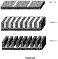
- Figures 1a-1c illustrates a chemoepitaxy process where the neutral layer is modified to define a patterned chemical affinity, Figure 1a .
- the block copolymer is then coated over a chemically modified neutral layer and annealed to form domains perpendicular to the substrate surface, Figure 1b .
- One of the domains is then removed to form a pattern on the surface of the substrate, Figure 1c .
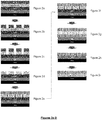
- Figure 2a- Figure 2i illustrates a novel process for forming line multiplication using a negative tone process.
- a multilayer stack is formed on a substrate in Figure 2a , where the stack comprises a substrate comprising a high carbon underlayer and a silicon antireflective coating layer, a crosslinked neutral layer and a photoresist layer. Any substrate may be used. Any neutral layer which is resistant to lithographic processes and maintains neutrality after crosslinking may be used.
- the photoresist may be any that is available such as 193nm photoresist, immersion 193nm photoresist, e beam photoresist, EUV photoresist, 248 nm photoresist, broadband, 365 nm, 436 nm, etc.
- the photoresist layer is imaged to form a pattern using conventional techniques.
- a negative tone photoresist may be used or a positive tone photoresist that uses an organic solvent to develop away the unexposed regions to form very narrow trenches may be used, as shown in Figure 2b .
- the novel underlayer is treated to form a pinning surface with a specific chemical affinity to one of the blocks of the novel block copolymer which has a molar ratio of repeat unit (1) to that of repeat unit (2) of 1.2 to 0.8 and which orient perpendicular to a neutral layer, using techniques such as plasma etching to remove the layer, plasma etching to modify the surface of the layer, or chemically treating the layer by further deposition of a material or any other pinning methods.
- a plasma comprising oxygen may be used to remove the neutral layer, as shown in Figure 2c .
- the photoresist is then stripped away using solvent stripper or plasma etching, as shown in Figure 2d .
- Solvents such as any organic solvents known for removing photoresists may be used, such as 1-Methoxy-2-propanol acetate (PGMEA), 1-Methoxy-2-propanol (PGME), ethyl lactate, etc.
- the photoresist may also be removed by developing the photoresist pattern in aqueous alkaline developer as commonly used in removing exposed photoresists.
- the neutral layer on the substrate still maintains its neutrality after the photoresist processing steps.
- the composition comprising the novel block copolymer is coated and treated (such as annealing) to form a self-directed alignment pattern of alternating segments of the novel block copolymer.
- a layer which is neutral is required to cause the alignment of the novel block copolymer to give regions of high etch resistance and regions of low etch resistance, such that pattern multiplication can be achieved, as shown in Figure 1e ; if the neutral layer was not sufficiently neutral then an undesirable orientation parallel to the surface would be achieved.
- a subsequent etch then removes the highly etchable blocks of the block copolymer, leaving a patterned surface with very high resolution, as shown in Figure 2f .
- Typical etch to remove one of the blocks would be a wet or plasma etch as described previously.
- the pattern may then be transferred into the lower stack layers by plasma etching, as shown in Figure 2g-2i , using etchants for the antireflective coating stack.
- Typical etch would be a plasma etch dependent on the substrate.
- Figure 3a to 3g illustrates a novel process for forming line multiplication using a positive tone process.
- a multilayer stack is formed on a substrate neutral layer and a photoresist layer in Figure 3a , where the substrate comprises a high carbon underlayer and a silicon antireflective coating layer.
- Any neutral layer which is resistant to lithographic processes and maintains neutrality after crosslinking may be used.
- the photoresist may be any that are available such as 193nm photoresist, immersion 193nm photoresist, e beam photoresist, EUV photoresist, 248 nm photoresist, etc.
- the photoresist layer is imaged to form a pattern using conventional techniques.
- a positive tone photoresist is used to form fine photoresist lines, as shown in Figure 3b .
- the photoresist is overexposed, that is given a high energy dose, to form very fine pattern.
- the very fine photoresist pattern over the novel neutral underlayer is used to form a self-aligned pattern using the novel block copolymer which has a molar ratio of repeat unit (1) to that of repeat unit (2) of 1.2 to 0.8 and which orient perpendicular to a neutral layer.
- the composition comprising the novel block copolymer is coated and treated (such as annealing) to form a self directed alignment pattern of alternating segments of the block copolymer.
- a layer which is neutral is required to cause the alignment of the block copolymer to give regions of high etch resistance and regions of low etch resistance, such that pattern multiplication can be achieved, as shown in Figure 3c ; if the neutral layer was not sufficiently neutral then an undesirable orientation perpendicular to one shown would be achieved.
- a subsequent etch then removes the highly etchable blocks of the novel block copolymer, leaving a patterned surface with very high resolution, as shown in Figure 3d .
- Typical etch would be a wet or plasma etch as described previously.
- the pattern may then be transferred into the lower stack layers by plasma etching, as shown in Figure 3e-g .
- Typical etch would be plasma etch dependent on the substrate.
- Figure 4a-4d illustrates a novel process for forming contact hole multiplication using a chemoepitaxy process.
- a multilayer stack is formed on a substrate, where the stack comprises a substrate (such as a silicon antireflective coating layer, a titanium antireflective coating, silicon oxide, etc,), a neutral layer and a photoresist layer.
- a neutral layer which is resistant to lithographic processes and maintains neutrality after crosslinking may be used.
- the photoresist may be any that are available such as 193nm photoresist, immersion 193nm photoresist, e beam photoresist, EUV photoresist, 248 nm photoresist, etc.
- the photoresist layer is imaged to form a pattern using conventional techniques, Figure 4a .
- the underlayer is treated to form a pinning surface using techniques such as plasma etching to remove the layer, plasma etching to modify the surface of the layer, or chemically treating the layer by further deposition of a material or any other pinning methods.
- a plasma comprising oxygen may be used to remove the neutral layer, as shown in Figure 4b .
- the photoresist is then stripped away using solvent stripper or plasma etching. Solvents such as any organic solvents known for removing photoresists, such as PGMEA, PGME, ethyl lactate, etc. may be used.
- the photoresist may also be used by developing the pattern in aqueous alkaline developer used in removing exposed photoresists.
- the neutral layer on the substrate still maintains its neutrality after the photoresist processing steps.
- the novel composition comprising novel block copolymer which has a molar ratio of repeat unit (1) to that of repeat unit (2) of 1.2 to 0.8 and which orient perpendicular to a neutral layer is coated and treated (such as annealing) to form a self-directed alignment contact hole pattern of alternating segments of the block copolymer.
- a layer which remains neutral is required to cause the desired orientation of the block copolymer to give regions of high etch resistance and regions of low etch resistance, such that pattern multiplication can be achieved; if the neutral layer was not sufficiently neutral then an undesirable orientation perpendicular to one shown would be achieved.
- a subsequent etch then removes the highly etchable blocks of the novel block copolymer, leaving a patterned surface with very high resolution, as shown in Figure 4d .
- Typical etch would be a wet or plasma etch as described previously.
- the pattern may then be transferred in the lower stack layers by plasma etching.
- Typical etch would be plasma etch dependent on the substrate. This process can be used for both pattern rectification and pattern pitch frequency multiplication.
- the general process for directed self-assembly useful for patterning which employs the novel block copolymer formulation described above comprises steps i) to iv) and where further the molar ratio in the novel block copolymer of repeat unit (1) to repeat unit (2) is between 5.3 to 8.
- an oriented block copolymer assembly is prepared where the microphase-separated domains that comprise cylindrical microdomains are oriented parallel to the substrate because the silicon rich domain has a preference to associate with the substrate.
- These microphase-separated domains having cylindrical domains oriented parallel to the substrate surface provide parallel line/space patterns during the block copolymer self-assembly.
- the domains, so oriented are thermally stable under further processing conditions.
- the domains of the block copolymer will form on and remain parallel to the neutral surface, giving highly resistant and highly etchable regions on the surface of the substrate, which can be further pattern transferred in the substrate layers.
- the directed self-assembled block copolymer pattern is transferred into the underlying substrate using known techniques. In one example wet or plasma etching could be used with optional UV exposure. Wet etching could be with acetic acid. Standard plasma etch process, such as a plasma comprising oxygen may be used; additionally argon, carbon monoxide, carbon dioxide, CF 4 , CHF 3 , may be present in the plasma.
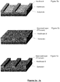
- a specific example of a graphoepitaxy approach as shown in Figure 5 may be employed to delineate lines and spaces by having a pattern previously formed by a resist in which the resist pattern surface has been treated with a hydroxy terminated polystyrene to form a polymer brush surface.
- Figure 5a to 5g illustrates a novel process for forming line multiplication using graphoepitaxial directed self-assembly (DSA) process.
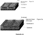
- Graphoepitaxial pre-pattern structure comprises a multilayer stack (Substrate and Hardmask B) and topographical guiding stripe patterns (Hardmask A) on it in Figure 5a , where the multilayer stack include materials such as a high carbon underlayer, silicon antireflective coating layer, Silicon Oxide, Silicon Nitride, Silicon Oxynitride and so on. Guiding topographical structure is made from same kind of material for multilayer stack or photoresist.
- brush material which has similar surface energy to one of domain in the BCP is coated and baked in as in Figure 5b and non-grafted excess brush materials are rinsed with organic solvents such as PGMEA, PGME, ethyl lactate, etc which retains topographical pre-pattern structure in Figure 5c .
- organic solvents such as PGMEA, PGME, ethyl lactate, etc which retains topographical pre-pattern structure in Figure 5c .
- the novel block copolymer solution is coated on chemically treated topographical pre-pattern in Figure 5d and annealed to form cylindrical morphology parallel to the substrate in Figure 5e .
- Lower etch resistant BCP domain which is typically non-silicon containing BCP domain, and thin brush layers except the area below the silicon containing domain are then removed to generate line patterns on the surface of the substrate in Figure 5f . Then, line patterns are transferred into underneath Hardmask B and substrate consecutively by plasma etching as in Figure 5g .
- any type of substrate may be used.
- a substrate which has a coating of high carbon underlayer and a silicon antireflective coating may be used as a substrate.
- the high carbon underlayer can have coating thickness of about 20 nm to about 2 microns. Over this is coated a silicon antireflective coating of about 10 nm to about 100 nm.
- a neutral layer may be employed.
- the molecular weight of the polymers was measured with a Gel Permeation Chromatograph.
- Poly(styrene-block-tert-butylmethacrylate) PS-b-PtBMA
- PS-b-PtBMA Poly(styrene-block-tert-butylmethacrylate)
- All other chemicals were obtained from the Aldrich Chemical Company (Sigma-Aldrich Corp St. Louis, MO, USA).
- the flask was immersed into a 90°C oil bath and hydrolysis was carried out at this temperature until Fourier Transform Infrared (FTIR) spectra showed no tert-butyl group CH peak at 1366 cm -1 .
- FTIR Fourier Transform Infrared
- the reaction solution was allowed to cool to room temperature and slowly poured into DI water under stirring.
- the resultant white polymer was isolated by filtering and washed thoroughly with DI water and methanol. Finally the polymer was dried in vacuum until constant weight to obtain 17 g PS-b-PMAA.
- the polymer was purified by dissolving in THF and precipitated in DI water. Finally the polymer was dried in 50°C vacuum oven until constant weight. 2.5 g of SiBCP was obtained. The polymer had a Mw of 38032 g/mol, a Mn of 36280 and PDI of 1.04.
- SiBCP made above was dissolved in PGMEA to prepare a 1.3 wt% solution.
- the solution was filtered with a 0.2 ⁇ m PTFE microfilter.
- the solution was spin cast on 6 inch silicon wafer at a rpm of 2200 for 30 seconds to obtain 28 nm thin film and the SiBCP film was annealed at 130°C in air for 5 min.
- the film was subject to 15 seconds of CF 4 plasma etch to remove the top Si wetting layer and then etched with 20 seconds of O 2 plasma to remove PS (etcher: MARCH etcher, Nordson Corp.).
Description
- The invention relates to compositions and processes for producing lines and spaces formed by directed self-assembly of block copolymers (BCP) containing a silicon block. The processes are useful for fabrication of electronic devices.
- Directed self-assembly of block copolymers is a method useful for generating smaller and smaller patterned features for the manufacture of microelectronic devices in which the critical dimensions (CD) of features on the order of nanoscale can be achieved. Directed self-assembly methods are desirable for extending the resolution capabilities of microlithographic technology. In a conventional lithography approach, ultraviolet (UV) radiation may be used to expose through a mask onto a photoresist layer coated on a substrate or layered substrate. Positive or negative photoresists are useful and these can also contain a refractory element such as silicon to enable dry development with conventional integrated circuit (IC) plasma processing. In a positive photoresist, UV radiation transmitted through a mask causes a photochemical reaction in the photoresist such that the exposed regions are removed with a developer solution or by conventional IC plasma processing. Conversely, in negative photoresists, UV radiation transmitted through a mask causes the regions exposed to radiation to become less removable with a developer solution or by conventional IC plasma processing. An integrated circuit feature, such as a gate, via or interconnect, is then etched into the substrate or layered substrate, and the remaining photoresist is removed. When using conventional lithographic exposure processes, the dimensions of features of the integrated circuit feature are limited. Further reduction in pattern dimensions are difficult to achieve with radiation exposure due to limitations related to aberrations, focus, proximity effects, minimum achievable exposure wavelengths and maximum achievable numerical apertures. The need for large-scale integration has led to a continued shrinking of the circuit dimensions and features in the devices. In the past, the final resolution of the features has been dependent upon the wavelength of light used to expose the photoresist, which has its own limitations. Direct assembly techniques, such as graphoepitaxy and chemoepitaxy using block copolymer imaging, are highly desirable techniques used to enhance resolution while reducing CD variation. These techniques can be employed to either enhance conventional UV lithographic techniques or to enable even higher resolution and CD control in approaches employing EUV, e-beam, deep UV or immersion lithography. The directed self-assembly block copolymer comprises a block of etch resistant copolymeric unit and a block of highly etchable copolymeric unit, which when coated, aligned and etched on a substrate give regions of very high density patterns.
- In the graphoepitaxy directed self-assembly method, the block copolymers self organizes around a substrate that is pre-patterned with conventional lithography (Ultraviolet, Deep UV, e-beam, Extreme UV (EUV) exposure source) to form repeating topographical features such as a line/space (L/S) or contact hole (CH) pattern. In an example of L/S directed self-assembly array, the block copolymer can form self-aligned lamellar regions which can form parallel line-space patterns of different pitches in the trenches between pre-patterned lines, thus enhancing pattern resolution by subdividing the space in the trench between the topographical lines into finer patterns. For example, a diblock copolymer which is capable of microphase separation and comprises a block rich in carbon (such as styrene or containing some other element like Si, Ge, Ti) which is resistant to plasma etch, and a block which is highly plasma etchable or removable, can provide a high resolution pattern definition. Examples of highly etchable blocks can comprise monomers which are rich in oxygen and which do not contain refractory elements, and are capable of forming blocks which are highly etchable, such as methyl methacrylate. The plasma etch gases used in the etching process of defining the self-assembly pattern typically are those used in processes to make integrated circuits (IC). In this manner very fine patterns can be created on typical IC substrates compared to conventional lithographic techniques, thus achieving pattern multiplication. Similarly, features such as contact holes can be made denser by using graphoepitaxy in which a suitable block copolymer arranges itself by directed self-assembly around an array of contact holes or posts defined by conventional lithography, thus forming a denser array of regions of etchable and etch resistant domains which when etched give rise to a denser array of contact holes. Consequently, graphoepitaxy has the potential to offer both pattern rectification and pattern multiplication.
- In chemical epitaxy or pinning chemical epitaxy, the self-assembly of the block copolymer is formed around a surface that has regions of differing chemical affinity but no or very slight topography to guide the self-assembly process. For example, the surface of a substrate could be patterned with conventional lithography (UV, Deep UV, e-beam EUV) to create surfaces of different chemical affinity in a line and space (L/S) pattern in which exposed areas whose surface chemistry had been modified by irradiation alternate with areas which are unexposed and show no chemical change. These areas present no topographical difference, but do present a surface chemical difference or pinning to direct self-assembly of block copolymer segments. Specifically, the directed self-assembly of a block copolymer whose block segments contain etch resistant (such as styrene repeat unit) and rapidly etching repeat units (such as methyl methacrylate repeat units) would allow precise placement of etch resistant block segments and highly etchable block segments over the pattern. This technique allows for the precise placement of these block copolymers and the subsequent pattern transfer of the pattern into a substrate after plasma or wet etch processing. Chemical epitaxy has the advantage that it can be fine tuned by changes in chemical differences to help improve line-edge roughness and CD control, thus allowing for pattern rectification. Other types of patterns such as repeating contact holes (CH) arrays could also be pattern rectified using chemoepitaxy.
- Neutral layers are layers on a substrate or the surface of a treated substrate which have no affinity for either of the block segment of a block copolymer employed in directed self-assembly. In the graphoepitaxy method of directed self-assembly of block copolymer, neutral layers are useful as they allow the proper placement or orientation of block polymer segments for directed self-assembly which leads to proper placement of etch resistant block polymer segments and highly etchable block polymer segments relative to the substrate. For instance, in surfaces containing line and space features which have been defined by conventional radiation lithography, a neutral layer allows block segments to be oriented so that the block segments are oriented perpendicular to the surface of the substrates, an orientation which is ideal for both pattern rectification and pattern multiplication depending on the length of the block segments in the block copolymer as related to the length between the lines defined by conventional lithography.
- The use of diblock copolymer of styrene and dimethylsiloxane having a high silicon content in a direct self-assembly process, where assembly of the high silicon contents enables plasma etch transfer of the self-assembled pattern into a substrate, requires either the use of solvent annealing (
US2011/0272381 ) to lower the annealing temperatures needed for self-assembly of the block domains or alternatively processing at high temperature (275-350°C) under gaseous conditions of low oxygen in which the oxygen content is equal or less than 7.5 ppm (US2013/0209344 ). Consequently, there is a need for a block copolymer containing a high silicon domain which can be processed at lower temperatures particularly when doing so in air. -
WO 88/09527 A2 -
US 2004/0006191 A1 discloses a silicon-containing polymer, resist composition and patterning process. This document discloses a silicon-containing polymer comprising recurring units of three components represented by the general formula (I). In addition, a silicon-containing polymer comprising recurring units of three components represented by the general formula (2). -
US 2013/0078576 A1 discloses compositions for directed self assembly block copolymers and processes thereof. A random copolymer is disclosed having at least one unit of structure (1), at least one unit of structure (2) and at least one unit of structure (3) as shown in this paragraph. R1 in structure (1) is selected from the group consisting of alkyl, fluoroalkyl, partially fluorinated alkyl, cycloalkyl, cyclofluoroalkyl, partially fluorinated cycloalkyl, and hydroxyalkyl. -
US 2013/0209693 A1 discloses a copolymer composition including a block copolymer having a poly(methyl methacrylate) block and a poly((trimethylsilyl)methyl methacrylate) block. (Trimethylsilyl)methyl methacrylate is shown in paragraph [0017] of this document. - When using a Graphoepitaxy approach to define an array of lines and spaces or contact holes or via using a conventional block copolymer materials, such as block copolymer of styrene and dimethylsiloxane, it is necessary to employ high temperatures or annealing with solvent. The present invention describes a novel block copolymer containing a high silicon content block which can be annealed at a lower range of temperature between 120°C and 250°C in air without the need of low oxygen or solvent annealing to affect the directed self-assembly needed which is required to create silicon rich and silicon free domains which may be used to pattern transfer lines and spaces, contact hole, vias or other features into a substrate. The invention also relates to compositions comprising this novel polymer and a solvent and processes to form a coating of the novel block polymer on a substrate.
- The present invention also relates to directed self-assembly processes for making lines and spaces, contact holes vias or other features into a substrate by using a composition containing the novel polymer of this invention.
-
-
Figures 1a-1c show a self-alignment process for the novel block copolymer which has a ratio of repeat unit (1) to that of repeat unit (2) of 1.2 to 0.8 and which orients perpendicular to a neutral layer. -
Figures 2a-2i show a process for negative tone line multiplication for the novel block copolymer which has a ratio of repeat unit (1) to that of repeat unit (2) of 1.2 to 0.8 and which orients perpendicular to a neutral layer. -
Figures 3a-3g show a process for positive tone multiplication for the novel block copolymer multiplication which has a ratio of repeat unit (1) to that of repeat unit (2) of 1.2 to 0.8 and which orients perpendicular to a neutral layer. -
Figures 4a-4d show a contact hole process for the novel block copolymer multiplication which has a ratio of repeat unit (1) to that of repeat unit (2) of 1.2 to 0.8 and which orients perpendicular to a neutral layer. -
Figures 5a-5g show a cylinder graphoepitaxy process for the novel block copolymer multiplication which has a ratio of repeat unit (1) to that of repeat unit (2) of 5.3 to 8 and which orients parallel to a substrate. - The present invention relates to a block copolymer comprising a repeat unit (1) and repeat unit (2), where R1 is hydrogen or C1-C4 alkyl, R2 is hydrogen, C1-C4alkyl, C1-C4alkoxy or halide, R3 is hydrogen, C1-C4 alkyl, or C1-C4fluoroalkyl, and R4, R5, R6, R7, R8, R9, R10, R11, and R12 are independently chosen from C1-C4 alkyl and n= 1-6.

- The present invention also relates to a novel composition comprising the novel block copolymer and a solvent. The present invention further relates to a process for employing this novel composition to affect directed self-assembly on a substrate to form silicon rich and silicon poor domains which is used to develop the self-assembled polymer structure to form a pattern array.
- As used herein, alkyl refers to saturated hydrocarbon groups which can be linear or branched (e.g. methyl, ethyl, propyl, isopropyl, tert-butyl and the like) or cycloalkyl refering to a hydrocarbon containing one saturated cycle (e.g. cyclohexyl, cyclopropyl, cyclopentyl and the like), fluoroalkyl refers to a linear or branched saturated alkyl group in which all the hydrogens have been replaced by fluorine, cyclofluoroalkyl refers to a cycloalkyl group in which all the hydrogens have been replaced by fluorine. The term "-b-" refers to "-block-" and designates monomer repeat units that form block copolymer.
- The present invention relates to a novel block copolymer comprising a repeat unit (1) and a repeat unit (2), where R1 is hydrogen or C1-C4 alkyl, R2 is selected from a group chosen from hydrogen, C1-C4 alkyl, C1-C4 alkoxy or halide, R3 is hydrogen, C1-C4 alkyl, or a C1-C4 fluoroalkyl, and R4, R5, R6, R7, R8, R9, R10, R11, and R12 are independently chosen from C1-C4 alkyl and n= 1-6.

- One aspect of this invention is where the block copolymer is a diblock copolymer.
- In another embodiment of this invention, particularly useful for a cylinder graphoepitaxy process in which the silicon rich domains self-assemble as cylinder domains parallel to the substrate along guiding graphoepitaxy lines, the novel block copolymer has a ratio of repeat unit (1) to that of repeat unit (2) in the range of about 5.3 to about 8.0. Another aspect of the invention is where the polymer has a Mn of 28,000 to 75,000 g/mole, and a polydispersity of 1.0 to 1.2.
- In a further embodiment of this aspect of the invention, the ratio of repeat unit (1) to that of repeat unit (2) is in the range of 5.3 to 8.0. In still another aspect of this invention the polymer has a Mn of 28,000 to 46,000 g/mole and a polydispersity of 1.0 to 1.2.
- In still another embodiment the ratio of repeat unit (1) to that of repeat unit (2) is in the range of 7.3 to 6.0. In another aspect of this embodiment the polymer has a Mn of 28,000 to 46,000 g/mole. In still another embodiment the polymer also a polydispersity of 1.0 to 1.2.
- In still another embodiment of this invention the block copolymer has a ratio of repeat units (1) to that of repeat unit (2) is in the range of 5.3 to 8.0 and where R1 is hydrogen, R2 is hydrogen or a C1-C4 alkyl, R3 is a C1-C4 alkyl or a C1-C4 fluoroalkyl, and R4, R5, R6, R7, R8, R9, R10, R11, and R12 are each a methyl and n=2-6. In a further embodiment of this invention R1 is hydrogen, R2 is hydrogen, R3 is a C1-C4 alkyl, and R4, R8, R6, R7, R8, R9, R10, R11, and R12 are each methyl and n=2-6. In a preferred embodiment of this invention R1 is hydrogen, R2 is hydrogen, R3 is a methyl, and R4, R5, R6, R7, R8, R9, R10, R11, and R12 are each methyl and n=3. In another aspect of this invention, the polymer has the above described restriction in substituents, a more narrow range of the repeat unit (1) to that of repeat unit (2) of 7.3 to 6.0 along with an Mn of 28,000 to 46,000 g/mole, and a polydispersity of 1.0 to 1.2.
- In another embodiment useful for conventional graphoepitaxy or chemoepitaxy in which the block copolymer self-assembles as cylinders perpendicular to the substrate along guiding graphoepitaxy lines, the novel block copolymer has a molar ratio of repeat unit (1) to repeat unit (2) of 1.2 to 0.8, an Mn of 28,000 to 75,000 g/mole, and a polydispersity of 1.0 to 1.2. In another embodiment of this, the molar ratio of repeat unit (1) to that repeat unit (2) is 1.2 to 0.8 and the polymer has a Mn of 28,000 to 46,000 g/mole and the polydispersity is 1.0 to 1.2. In a further embodiment of this, the molar ratio of repeat unit (1) to that of repeat unit (2) is from 0.9 to 1.1 and the polymer has a Mn of 28,000 to 46,000 g/mole and a polydispersity of 1.0 to 1.2.
- In still another embodiment of this invention the block copolymer has a ratio of repeat units (1) to that of repeat unit (2) of 1.2 to 0.8, and the repeat units (1) and (2) are ones in which R1 is hydrogen, R2 is hydrogen or a C1-C4 alkyl, R3 is a C1-C4alkyl or a C1-C4 fluoroalkyl, and R4, R5, R6, R7, R8, R9, R10, R11, and R12 are methyls and n=2-6. In a further embodiment of this invention R1 is hydrogen, R2 is hydrogen, R3 is a C1-C4alkyl, and R4, R5, R6, R7, R8, R9, R10, R11, and R12 are methyls and n=2-6. In another embodiment of this invention R1 is hydrogen, R2 is hydrogen, R3 is a methyl, and R4, R5, R6, R7, R8, R9, R10, R11, and R12 are methyls and n= 3.
- In yet another embodiment of the present invention is where the polymer has a molar ratio of repeat unit (1) to that of repeat unit (2) from 1.2 to 0.8 and also has the above restriction in substituents along with the above described embodiment of Mn and polydispersity.
- The novel block copolymer of this invention comprising repeat unit (1) and repeat unit (2) may be made with a living anionic polymerization respectively from the corresponding monomers I and monomers II using conventional block copolymerization techniques applicable to the forming block copolymers of styrene and alkyl methacrylate (see Nagaki, Aiichiro; Miyazaki, Atsuo; Yoshida, Jun-ichi from Macromolecules (Washington, DC, United States) (2010), 43(20), 8424-8429 and reference therein).
- Alternatively, the block copolymer of this invention may be made by polymer modification of another block copolymer precursor. Scheme 1 outlines a non-limiting example of such a polymer modification which employs as starting material a block copolymer of tert-butyl methacrylate and styrene which yield the embodiment of the present invention where the block copolymer has a molar ratio of repeat unit (1) to repeat unit (2) of 0.8 to 1.2 or 5.3 to 8.0 and where R1 is hydrogen, R2 is hydrogen, R3 is a methyl, and R4, R5, R6, R7, R8, R9, R10, R11, and R12 are each methyl and n= 3.

- The novel block copolymer of the present invention is formulated in a composition comprising the novel block copolymer and a solvent.
- Examples of suitable solvents are conventional spin casting solvents based upon esters, alcoholic esters, ethers, alcoholic ether, lactones or mixtures of these.
- More specific examples are 1,2-propanediol alkyl ethers where the alkyl group is a C1-C4 alkyl moiety; alkylcarboxylate ester of 1,2-propanediol alkyl ethers where the alkyl group is a C1-C4 alkyl moiety; alkyl acetates where the alkyl group is a C1-C4 alkyl moiety; alkyl benzenes where the alkyl group is a C1-C4 alkyl moiety, C8-C12 alkanes, C6-C12 cycloalkanes, and mixtures thereof and the like.
- Other specific examples are solvents such as propylene glycol methyl ether acetate, propyleneglycol methyl ether, n-butyl acetate, gamma-butyrolactone, anisol, 2-heptanone, xylene, anisole, decalin, cyclohexane, cyclohexene, methylcyclohexane, ethylcyclohexane, limonene, hexane, octane, nonane, decane, or mixtures of these.
- The novel block copolymer of the present invention is dissolved in the solvent(s) as a solution, where the block copolymer has a concentration in the solvent between 0.5 to 5 wt % of the total composition. In another embodiment the concentration of the block copolymer is between 0.5 to 1.5 wt% of the total composition.
- The block copolymer composition can comprise additional components and/or additives selected from the group consisting of: inorganic-containing polymers; additives including small molecules, inorganic-containing molecules, surfactants, photoacid generators, thermal acid generators, quenchers, hardeners, cross-linkers, chain extenders, and the like; and combinations comprising at least one of the foregoing, wherein one or more of the additional components and/or additives co-assemble with the block copolymer to form the block copolymer assembly.
- The composition may further comprise additives such as surfactants.
- A general process for directed self-assembly useful for patterning which employs the novel block copolymer formulation described above comprises steps i) to iv); wherein,
- i) coating the block copolymer composition over a substrate to form a film;
- ii) applying a flow bake to the block copolymer film to remove solvent and to optionally conformably coat any topography in the substrate;
- iii) applying an annealing bake to affect self-assembly of the block copolymer; and,
- iv) developing the self assembled polymer structure to form a pattern array.
- The application of the novel block copolymer in step i) onto a substrate is done by spinning techniques (including spin drying). Self-directed domain formation can occur during the flow baking, annealing, or during a combination of one or more of these operations (steps ii and iii).
- In one embodiment, the film spun from the novel block copolymer is subjected to a flow bake (step ii) in the range of between 100°C and 160C in air followed by an annealing bake (step iii) in the range of 120°C and 250°C also done in air without need for solvent annealing or a low oxygen environment. In another embodiment the annealing bake in air is done between in the range of 180°C and 250°C also without the need of solvent annealing or a low oxygen environment.
- Alternatively, the annealing (step iii) can be conducted between 120°C and 300°C and is done in nitrogen without need of solvent annealing. In another embodiment the annealing bake in air is done between 180°C and 300°C without need of solvent annealing.
- The present invention further relates to an embodiment of the novel process which employs the novel block copolymer in which the molar ratio in the novel block copolymer of repeat unit (1) to repeat unit (2) is between 1.2 to 0.8 (as described above in all its possible embodiments) and where the oriented block copolymer assembly is prepared by the above process, having microphase-separated domains that comprise cylindrical microdomains oriented perpendicular to the neutral surface because neither domain has any preference to associate with the neutral layer. The microphase-separated domains have lamellar domains oriented perpendicular to the neutral surface, which provide parallel line/space patterns in the block copolymer assembly. The domains, so oriented, are thermally stable under further processing conditions. Thus, after coating a layer of the novel block copolymer and assembly including, baking and/or annealing, the domains of the block copolymer will form on and remain perpendicular to the neutral surface, giving highly resistant and highly etchable regions on the surface of the substrate, which can be further pattern transferred in the substrate layers. The directed self-assembled block copolymer pattern is transferred into the underlying substrate using known techniques. In one example wet or plasma etching could be used with optional UV exposure. Wet etching could be with acetic acid. Standard plasma etch process, such as a plasma comprising oxygen may be used; additionally argon, carbon monoxide, carbon dioxide, CF4, CHF3, may be present in the plasma.
Figures 1a-1c illustrates a chemoepitaxy process where the neutral layer is modified to define a patterned chemical affinity,Figure 1a . The block copolymer is then coated over a chemically modified neutral layer and annealed to form domains perpendicular to the substrate surface,Figure 1b . One of the domains is then removed to form a pattern on the surface of the substrate,Figure 1c . -
Figure 2a-Figure 2i illustrates a novel process for forming line multiplication using a negative tone process. A multilayer stack is formed on a substrate inFigure 2a , where the stack comprises a substrate comprising a high carbon underlayer and a silicon antireflective coating layer, a crosslinked neutral layer and a photoresist layer. Any substrate may be used. Any neutral layer which is resistant to lithographic processes and maintains neutrality after crosslinking may be used. The photoresist may be any that is available such as 193nm photoresist, immersion 193nm photoresist, e beam photoresist, EUV photoresist, 248 nm photoresist, broadband, 365 nm, 436 nm, etc. The photoresist layer is imaged to form a pattern using conventional techniques. A negative tone photoresist may be used or a positive tone photoresist that uses an organic solvent to develop away the unexposed regions to form very narrow trenches may be used, as shown inFigure 2b . The novel underlayer is treated to form a pinning surface with a specific chemical affinity to one of the blocks of the novel block copolymer which has a molar ratio of repeat unit (1) to that of repeat unit (2) of 1.2 to 0.8 and which orient perpendicular to a neutral layer, using techniques such as plasma etching to remove the layer, plasma etching to modify the surface of the layer, or chemically treating the layer by further deposition of a material or any other pinning methods. A plasma comprising oxygen may be used to remove the neutral layer, as shown inFigure 2c . The photoresist is then stripped away using solvent stripper or plasma etching, as shown inFigure 2d . Solvents such as any organic solvents known for removing photoresists may be used, such as 1-Methoxy-2-propanol acetate (PGMEA), 1-Methoxy-2-propanol (PGME), ethyl lactate, etc. The photoresist may also be removed by developing the photoresist pattern in aqueous alkaline developer as commonly used in removing exposed photoresists. The neutral layer on the substrate still maintains its neutrality after the photoresist processing steps. Over the patterned neutral layer,Figure 2e , the composition comprising the novel block copolymer is coated and treated (such as annealing) to form a self-directed alignment pattern of alternating segments of the novel block copolymer. A layer which is neutral is required to cause the alignment of the novel block copolymer to give regions of high etch resistance and regions of low etch resistance, such that pattern multiplication can be achieved, as shown inFigure 1e ; if the neutral layer was not sufficiently neutral then an undesirable orientation parallel to the surface would be achieved. A subsequent etch then removes the highly etchable blocks of the block copolymer, leaving a patterned surface with very high resolution, as shown inFigure 2f . Typical etch to remove one of the blocks would be a wet or plasma etch as described previously. The pattern may then be transferred into the lower stack layers by plasma etching, as shown inFigure 2g-2i , using etchants for the antireflective coating stack. Typical etch would be a plasma etch dependent on the substrate. -
Figure 3a to 3g illustrates a novel process for forming line multiplication using a positive tone process. A multilayer stack is formed on a substrate neutral layer and a photoresist layer inFigure 3a , where the substrate comprises a high carbon underlayer and a silicon antireflective coating layer. Any neutral layer which is resistant to lithographic processes and maintains neutrality after crosslinking may be used. The photoresist may be any that are available such as 193nm photoresist, immersion 193nm photoresist, e beam photoresist, EUV photoresist, 248 nm photoresist, etc. The photoresist layer is imaged to form a pattern using conventional techniques. A positive tone photoresist is used to form fine photoresist lines, as shown inFigure 3b . In some cases the photoresist is overexposed, that is given a high energy dose, to form very fine pattern. The very fine photoresist pattern over the novel neutral underlayer is used to form a self-aligned pattern using the novel block copolymer which has a molar ratio of repeat unit (1) to that of repeat unit (2) of 1.2 to 0.8 and which orient perpendicular to a neutral layer. The composition comprising the novel block copolymer is coated and treated (such as annealing) to form a self directed alignment pattern of alternating segments of the block copolymer. A layer which is neutral is required to cause the alignment of the block copolymer to give regions of high etch resistance and regions of low etch resistance, such that pattern multiplication can be achieved, as shown inFigure 3c ; if the neutral layer was not sufficiently neutral then an undesirable orientation perpendicular to one shown would be achieved. A subsequent etch then removes the highly etchable blocks of the novel block copolymer, leaving a patterned surface with very high resolution, as shown inFigure 3d . Typical etch would be a wet or plasma etch as described previously. The pattern may then be transferred into the lower stack layers by plasma etching, as shown inFigure 3e-g . Typical etch would be plasma etch dependent on the substrate. -
Figure 4a-4d illustrates a novel process for forming contact hole multiplication using a chemoepitaxy process. A multilayer stack is formed on a substrate, where the stack comprises a substrate (such as a silicon antireflective coating layer, a titanium antireflective coating, silicon oxide, etc,), a neutral layer and a photoresist layer. A neutral layer which is resistant to lithographic processes and maintains neutrality after crosslinking may be used. The photoresist may be any that are available such as 193nm photoresist, immersion 193nm photoresist, e beam photoresist, EUV photoresist, 248 nm photoresist, etc. The photoresist layer is imaged to form a pattern using conventional techniques,Figure 4a . The underlayer is treated to form a pinning surface using techniques such as plasma etching to remove the layer, plasma etching to modify the surface of the layer, or chemically treating the layer by further deposition of a material or any other pinning methods. A plasma comprising oxygen may be used to remove the neutral layer, as shown inFigure 4b . The photoresist is then stripped away using solvent stripper or plasma etching. Solvents such as any organic solvents known for removing photoresists, such as PGMEA, PGME, ethyl lactate, etc. may be used. The photoresist may also be used by developing the pattern in aqueous alkaline developer used in removing exposed photoresists. The neutral layer on the substrate still maintains its neutrality after the photoresist processing steps. Over the patterned neutral layer,Figure 4c , the novel composition comprising novel block copolymer which has a molar ratio of repeat unit (1) to that of repeat unit (2) of 1.2 to 0.8 and which orient perpendicular to a neutral layer is coated and treated (such as annealing) to form a self-directed alignment contact hole pattern of alternating segments of the block copolymer. A layer which remains neutral is required to cause the desired orientation of the block copolymer to give regions of high etch resistance and regions of low etch resistance, such that pattern multiplication can be achieved; if the neutral layer was not sufficiently neutral then an undesirable orientation perpendicular to one shown would be achieved. A subsequent etch then removes the highly etchable blocks of the novel block copolymer, leaving a patterned surface with very high resolution, as shown inFigure 4d . Typical etch would be a wet or plasma etch as described previously. The pattern may then be transferred in the lower stack layers by plasma etching. Typical etch would be plasma etch dependent on the substrate. This process can be used for both pattern rectification and pattern pitch frequency multiplication. - Another aspect of this invention is where, the general process for directed self-assembly useful for patterning which employs the novel block copolymer formulation described above comprises steps i) to iv) and where further the molar ratio in the novel block copolymer of repeat unit (1) to repeat unit (2) is between 5.3 to 8. In this instance however an oriented block copolymer assembly is prepared where the microphase-separated domains that comprise cylindrical microdomains are oriented parallel to the substrate because the silicon rich domain has a preference to associate with the substrate. These microphase-separated domains having cylindrical domains oriented parallel to the substrate surface provide parallel line/space patterns during the block copolymer self-assembly. The domains, so oriented, are thermally stable under further processing conditions. Thus, after coating a layer of the novel block copolymer and self-assembly including, baking and/or annealing, the domains of the block copolymer will form on and remain parallel to the neutral surface, giving highly resistant and highly etchable regions on the surface of the substrate, which can be further pattern transferred in the substrate layers. The directed self-assembled block copolymer pattern is transferred into the underlying substrate using known techniques. In one example wet or plasma etching could be used with optional UV exposure. Wet etching could be with acetic acid. Standard plasma etch process, such as a plasma comprising oxygen may be used; additionally argon, carbon monoxide, carbon dioxide, CF4, CHF3, may be present in the plasma. A specific example of a graphoepitaxy approach as shown in
Figure 5 may be employed to delineate lines and spaces by having a pattern previously formed by a resist in which the resist pattern surface has been treated with a hydroxy terminated polystyrene to form a polymer brush surface. -
Figure 5a to 5g illustrates a novel process for forming line multiplication using graphoepitaxial directed self-assembly (DSA) process. Graphoepitaxial pre-pattern structure comprises a multilayer stack (Substrate and Hardmask B) and topographical guiding stripe patterns (Hardmask A) on it inFigure 5a , where the multilayer stack include materials such as a high carbon underlayer, silicon antireflective coating layer, Silicon Oxide, Silicon Nitride, Silicon Oxynitride and so on. Guiding topographical structure is made from same kind of material for multilayer stack or photoresist. To align parallel cylindrical BCP to the substrate in the trench, brush material (Alignment layer) which has similar surface energy to one of domain in the BCP is coated and baked in as inFigure 5b and non-grafted excess brush materials are rinsed with organic solvents such as PGMEA, PGME, ethyl lactate, etc which retains topographical pre-pattern structure inFigure 5c . Then the novel block copolymer solution is coated on chemically treated topographical pre-pattern inFigure 5d and annealed to form cylindrical morphology parallel to the substrate inFigure 5e . Lower etch resistant BCP domain, which is typically non-silicon containing BCP domain, and thin brush layers except the area below the silicon containing domain are then removed to generate line patterns on the surface of the substrate inFigure 5f . Then, line patterns are transferred into underneath Hardmask B and substrate consecutively by plasma etching as inFigure 5g . - In the above processes, any type of substrate may be used. As an example, a substrate which has a coating of high carbon underlayer and a silicon antireflective coating may be used as a substrate. The high carbon underlayer can have coating thickness of about 20 nm to about 2 microns. Over this is coated a silicon antireflective coating of about 10 nm to about 100 nm. In instances where an orientation of the self assembled cylinder of the novel block copolymer perpendicular to the substrate is desired a neutral layer may be employed.
- The following specific examples will provide detailed illustrations of the methods of producing and utilizing compositions of the present invention. These examples are not intended, however, to limit or restrict the scope of the invention in any way and should not be construed as providing conditions, parameters or values which must be utilized exclusively in order to practice the present invention.
- The molecular weight of the polymers was measured with a Gel Permeation Chromatograph. Poly(styrene-block-tert-butylmethacrylate) (PS-b-PtBMA) was bought from Polymer Source Inc. 124 Avro Street, Dorval (Montreal), Quebec H9P 2X8, Canada. All other chemicals were obtained from the Aldrich Chemical Company (Sigma-Aldrich Corp St. Louis, MO, USA).
- Spinning and baking of films was done with Laurel WS-650-23B spin coater and a Tokyo Electron Ltd. Clean Track ACT-8. Nordson (300 Nordson Dr. M/S 47 Amherst, OH 44001 U.S.A. MARCH etcher was used for plasma etching of non-Si containing domain. Top down and cross section images were taken on AMAT (Applied Materials, Inc. 3050 Bowers Avenue P.O. Box 58039 Santa Clara, CA 95054-3299 U.S.A.) NanoSEM 3D and Hitachi (Hitachi High Technologies America Inc. 10 North Martingale Road, Suite 500 Schaumburg, Illinois 60173-2295) S-5500, respectively.
- 20.14 g of PS-b-PtBMA (Mn for PS block was 29290 g/mol by GPC, Mn for PtBMA was 6000 g/mol estimated by NMR and PDI was 1.04) was dissolved in 320 g of 1,4-dioxane in a 500 ml flask with a magnetic stirring bar and a cold water condenser. To this solution was added 60 ml of 4M HCI in dioxane and 15 g of deiozined (DI) water. The flask was immersed into a 90°C oil bath and hydrolysis was carried out at this temperature until Fourier Transform Infrared (FTIR) spectra showed no tert-butyl group CH peak at 1366 cm-1. The reaction solution was allowed to cool to room temperature and slowly poured into DI water under stirring. The resultant white polymer was isolated by filtering and washed thoroughly with DI water and methanol. Finally the polymer was dried in vacuum until constant weight to obtain 17 g PS-b-PMAA.
- 12 g of PS-b-PMAA prepared above was dissolved in 110 g of 1,4-dioxane and 36 g of THF in a 250 ml flask with a magnetic bar. To this solution was added 6 g of tetramethylammonium pentahydrate dissolved in 30 g of methanol. After the mixture was stirred at room temperature for 7 hours, 13 g of allyl iodide was added. The reaction mixture was stirred at room temperature for 2 days. The formed tetramethylammonium iodide was filtered out. The filtrate was poured into methanol under stirring. The resultant polymer was isolated by filtering and washed thoroughly with methanol. After drying in vacuum, 11.2 g of PS-b-PAMA was obtained. The polymer had a Mw of 34484 g/mol, a Mn of 33091 and PDI of 1.04.
- 2.3 g of PS-b-PAMA prepared above was dissolved in toluene to prepare a 10 wt% solution. 3.25 g of 5 wt % dodecanethiol in toluene and 11.6 g of tris(trimethylsilyl) silane were added. After the mixture was cooled to 0 °C in an ice bath, 3.2 g of 1M triethylborane in hexane was added in small portions over 2 hrs. After addition, the ice bath was removed and the reaction mixture was stirred at room temperature overnight. The mixture was poured into methanol under stirring. The resultant polymer was isolated by filtering and washed thoroughly by methanol. The polymer was purified by dissolving in THF and precipitated in DI water. Finally the polymer was dried in 50°C vacuum oven until constant weight. 2.5 g of SiBCP was obtained. The polymer had a Mw of 38032 g/mol, a Mn of 36280 and PDI of 1.04.
- SiBCP made above was dissolved in PGMEA to prepare a 1.3 wt% solution. The solution was filtered with a 0.2 µm PTFE microfilter. The solution was spin cast on 6 inch silicon wafer at a rpm of 2200 for 30 seconds to obtain 28 nm thin film and the SiBCP film was annealed at 130°C in air for 5 min. The film was subject to 15 seconds of CF4 plasma etch to remove the top Si wetting layer and then etched with 20 seconds of O2 plasma to remove PS (etcher: MARCH etcher, Nordson Corp.). Self - assembly line pattern were observed under NanoSEM, indicating that the SiBCP was thermally annealable and formed parallel BCP cylinder finger print morphology for line patterns with regards to the substrate because a perpendicular BCP cylinder morphology with regards to the substrate would have generated a pattern of random holes.
Claims (15)
- A composition for use in directed self-assembly comprising;i) a block copolymer comprising a repeat unit of structure (1) and a repeat unit of structure (2), where R1 is hydrogen or C1-C4 alkyl, R2 is selected from a group chosen from hydrogen, C1-C4 alkyl, C1-C4 alkoxy and halide, R3 is selected from a group chosen from hydrogen, C1-C4 alkyl and C1-C4 fluoroalkyl, and R4, R5, R6, R7, R8, R9, R10, R11, and R12 are independently chosen from C1-C4 alkyl and n= 1-6; preferably R1 is hydrogen, R2 is hydrogen or C1-C4 alkyl, R3 is C1-C4 alkyl or C1-C4 fluoroalkyl, and R4, R5, R6, R7, R8, R9, R10, R11, and R12 are each methyl and n=2-6, and
 ii) solvent.
 - The composition according to claim 1 where the block copolymer has a molar ratio of repeat unit (1) to repeat unit (2) in the range of 1.2 to 0.8.
- The composition according to claim 1 or 2 where R1 is hydrogen, R2 is hydrogen, R3 is C1-C4 alkyl, and R4, R5, R6, R7, R8, R9, R10, R11, and R12 are each methyl and n=2-6, preferably R1 is hydrogen, R2 is hydrogen, R3 is methyl, and R4, R5, R6, R7, R8, R9, R10, R11, and R12 are each methyl and n= 3.
- The composition according to any of claims 1 to 3 where the block copolymer has a molar ratio of repeat unit (1) to repeat unit (2) in the range of 5.3 to 8.0, preferably in the range of 7.3 to 6.0.
- The composition according to any of claims 1 to 4 wherein the concentration of the block copolymer in the solvent is between 0.5 to 5 wt % of the total composition.
- The composition according to any of claims 1 to 5 where the solvent is selected from a group chosen from 1,2-propanediol C1-C4 alkyl ether C1-C4 alkylcarboxylate, C1-C4 alkyl C1-C4 alkylcarboxylate and mixtures thereof.
- A process for directed self-assembly patterning comprising steps of;i) coating the block copolymer composition according to any of claims 1 to 6 over a substrate to form a block copolymer film;ii) applying a flow bake to the block copolymer film;iii) applying an annealing bake to cause self-assembly of the block copolymer; and,iv) developing the self-assembled polymer structure to form a pattern array.
- The process of claim 7 where in step iv) the development is done by dry plasma etching with a plasma containing oxygen.
- The process of claim 7 or 8 where in step ii) the flow bake is in the range of 100°C to 160°C.
- The process according to any of claims 7 to 9 where in step iii) the annealing bake is in the range of 150°C to 200°C and is done in air.
- The process according to any of claims 7 to 9 where in step iii) the annealing bake is in the range of 150°C to 250°C and is done in nitrogen.
- A block copolymer comprising a repeat unit (1) and a repeat unit (2), where R1 is hydrogen or C1-C4 alkyl, R2 is selected from a group chosen from hydrogen, C1-C4 alkyl, C1-C4 alkoxy and halide, R3 is selected from a group chosen from hydrogen, C1-C4 alkyl and C1-C4fluoroalkyl, and R4, R5, R6, R7, R8, R9, R10, R11, and R12 are independently chosen from a C1-C4alkyl and n= 1-6.

- The block copolymer according to claim 12 where the block copolymer has a molar ratio of repeat unit (1) to repeat unit (2) of 5.3 to 8.0, preferably in the range of 7.3 to 6.0.
- The block copolymer according to claim 12 or 13 where R1 is hydrogen, R2 is hydrogen or C1-C4 alkyl, R3 is C1-C4 alkyl or C1-C4fluoroalkyl, and R4, R5, R6, R7, R8, R9, R10, R11, and R12 are each methyl and n=2-6.
- The block copolymer according to any of claims 12 to 14 where the block copolymer has a molar ratio of repeat unit (1) to repeat unit (2) of 1.2 to 0.8.
Applications Claiming Priority (2)
| Application Number | Priority Date | Filing Date | Title |
|---|---|---|---|
| US14/527,939 US9505945B2 (en) | 2014-10-30 | 2014-10-30 | Silicon containing block copolymers for direct self-assembly application |
| PCT/EP2015/074980 WO2016066684A1 (en) | 2014-10-30 | 2015-10-28 | Silicon containing block copolymers for direct self-assembly application |
Publications (2)
| Publication Number | Publication Date |
|---|---|
| EP3212714A1 EP3212714A1 (en) | 2017-09-06 |
| EP3212714B1 true EP3212714B1 (en) | 2019-03-06 |
Family
ID=54541022
Family Applications (1)
| Application Number | Title | Priority Date | Filing Date |
|---|---|---|---|
| EP15794100.6A Active EP3212714B1 (en) | 2014-10-30 | 2015-10-28 | Silicon containing block copolymers for direct self-assembly application |
Country Status (9)
| Country | Link |
|---|---|
| US (1) | US9505945B2 (en) |
| EP (1) | EP3212714B1 (en) |
| JP (2) | JP6782695B2 (en) |
| KR (1) | KR102226229B1 (en) |
| CN (1) | CN107075057B (en) |
| IL (1) | IL250995A0 (en) |
| SG (1) | SG11201701937RA (en) |
| TW (1) | TWI677526B (en) |
| WO (1) | WO2016066684A1 (en) |
Families Citing this family (7)
| Publication number | Priority date | Publication date | Assignee | Title |
|---|---|---|---|---|
| US9738765B2 (en) * | 2015-02-19 | 2017-08-22 | International Business Machines Corporation | Hybrid topographical and chemical pre-patterns for directed self-assembly of block copolymers |
| WO2018101730A1 (en) * | 2016-11-30 | 2018-06-07 | 주식회사 엘지화학 | Block copolymer |
| KR102096272B1 (en) * | 2016-11-30 | 2020-04-02 | 주식회사 엘지화학 | Block copolymer |
| WO2018114930A1 (en) | 2016-12-21 | 2018-06-28 | AZ Electronic Materials (Luxembourg) S.à.r.l. | Novel compositions and processes for self-assembly of block copolymers |
| JP7076701B2 (en) * | 2018-03-05 | 2022-05-30 | 東京応化工業株式会社 | A block copolymer and a method for producing the same, and a method for producing a structure including a phase-separated structure. |
| FR3089982A1 (en) * | 2018-12-12 | 2020-06-19 | Arkema France | Method for manufacturing a block copolymer containing silicon |
| TW202307048A (en) | 2021-05-18 | 2023-02-16 | 德商馬克專利公司 | Hydrophobic crosslinkable pinning underlayers with improved dry etch capabilities for patterning directed self-assembly of ps-b-pmma type block copolymers |
Family Cites Families (19)
| Publication number | Priority date | Publication date | Assignee | Title |
|---|---|---|---|---|
| JPH02500152A (en) * | 1987-05-21 | 1990-01-18 | ヒューズ・エアクラフト・カンパニー | Silicon-containing negative resist materials and processing methods for patterning substrates |
| US5985524A (en) * | 1997-03-28 | 1999-11-16 | International Business Machines Incorporated | Process for using bilayer photoresist |
| US6210856B1 (en) * | 1999-01-27 | 2001-04-03 | International Business Machines Corporation | Resist composition and process of forming a patterned resist layer on a substrate |
| JP3963623B2 (en) * | 1999-12-09 | 2007-08-22 | 富士フイルム株式会社 | Positive photoresist composition |
| JP3858968B2 (en) * | 2000-01-06 | 2006-12-20 | 信越化学工業株式会社 | Method for producing tris (trimethylsilyl) silylethyl ester |
| US6291696B2 (en) * | 2000-01-06 | 2001-09-18 | Shin-Etsu Chemical Co., Ltd. | Preparation of tris (trimethylsilyl) silylethyl esters |
| US6444408B1 (en) * | 2000-02-28 | 2002-09-03 | International Business Machines Corporation | High silicon content monomers and polymers suitable for 193 nm bilayer resists |
| JP3781960B2 (en) | 2000-09-29 | 2006-06-07 | 信越化学工業株式会社 | Antireflection film material and pattern forming method |
| JP3912512B2 (en) * | 2002-07-02 | 2007-05-09 | 信越化学工業株式会社 | Silicon-containing polymer compound, resist material, and pattern forming method |
| JP4040392B2 (en) | 2002-08-22 | 2008-01-30 | 富士フイルム株式会社 | Positive photoresist composition |
| US8696918B2 (en) | 2010-05-05 | 2014-04-15 | Micron Technology, Inc. | Methods of utilizing block copolymer to form patterns |
| US8691925B2 (en) * | 2011-09-23 | 2014-04-08 | Az Electronic Materials (Luxembourg) S.A.R.L. | Compositions of neutral layer for directed self assembly block copolymers and processes thereof |
| US8961918B2 (en) | 2012-02-10 | 2015-02-24 | Rohm And Haas Electronic Materials Llc | Thermal annealing process |
| US8697810B2 (en) | 2012-02-10 | 2014-04-15 | Rohm And Haas Electronic Materials Llc | Block copolymer and methods relating thereto |
| US8710150B2 (en) | 2012-02-10 | 2014-04-29 | Rohm And Haas Electronic Materials Llc | Blended block copolymer composition |
| JP5745439B2 (en) * | 2012-02-17 | 2015-07-08 | 富士フイルム株式会社 | Actinic ray-sensitive or radiation-sensitive resin composition, pattern formation method using the same, resist film, and electronic device manufacturing method |
| US10000664B2 (en) * | 2012-03-27 | 2018-06-19 | Nissan Chemical Industries, Ltd. | Underlayer film-forming composition for self-assembled films |
| US8822619B1 (en) * | 2013-02-08 | 2014-09-02 | Rohm And Haas Electronic Materials Llc | Directed self assembly copolymer composition and related methods |
| JP5956370B2 (en) | 2013-03-12 | 2016-07-27 | 信越化学工業株式会社 | Silicon-containing underlayer film material and pattern forming method |
-
2014
- 2014-10-30 US US14/527,939 patent/US9505945B2/en active Active
-
2015
- 2015-10-28 CN CN201580057241.2A patent/CN107075057B/en active Active
- 2015-10-28 SG SG11201701937RA patent/SG11201701937RA/en unknown
- 2015-10-28 KR KR1020177014791A patent/KR102226229B1/en active IP Right Grant
- 2015-10-28 WO PCT/EP2015/074980 patent/WO2016066684A1/en active Application Filing
- 2015-10-28 JP JP2017523324A patent/JP6782695B2/en active Active
- 2015-10-28 EP EP15794100.6A patent/EP3212714B1/en active Active
- 2015-10-30 TW TW104135931A patent/TWI677526B/en active
-
2017
- 2017-03-07 IL IL250995A patent/IL250995A0/en unknown
-
2019
- 2019-10-23 JP JP2019192457A patent/JP6810782B2/en active Active
Non-Patent Citations (1)
| Title |
|---|
| None * |
Also Published As
| Publication number | Publication date |
|---|---|
| JP2020033566A (en) | 2020-03-05 |
| KR102226229B1 (en) | 2021-03-10 |
| CN107075057B (en) | 2019-02-15 |
| WO2016066684A1 (en) | 2016-05-06 |
| US9505945B2 (en) | 2016-11-29 |
| IL250995A0 (en) | 2017-04-30 |
| JP6810782B2 (en) | 2021-01-06 |
| SG11201701937RA (en) | 2017-04-27 |
| JP2018502936A (en) | 2018-02-01 |
| TWI677526B (en) | 2019-11-21 |
| EP3212714A1 (en) | 2017-09-06 |
| TW201619278A (en) | 2016-06-01 |
| JP6782695B2 (en) | 2020-11-11 |
| KR20170081206A (en) | 2017-07-11 |
| US20160122579A1 (en) | 2016-05-05 |
| CN107075057A (en) | 2017-08-18 |
Similar Documents
| Publication | Publication Date | Title |
|---|---|---|
| EP3212714B1 (en) | Silicon containing block copolymers for direct self-assembly application | |
| TWI599582B (en) | Novel compositions and processes for self-assembly of block copolymers | |
| JP6077547B2 (en) | Neutral layer composition for derivatized self-assembled block copolymer and method thereof | |
| TWI617890B (en) | A composition comprising a polymeric thermal acid generator and processes thereof | |
| KR20150008098A (en) | Silicon hardmask layer for directed self-assembly | |
| KR102409830B1 (en) | Polymer Compositions for Self-Assembly Applications | |
| JP2018503241A (en) | Defect reduction methods and compositions for induced self-assembly patterning | |
| EP3523823A1 (en) | Chemically patterned guide layers for use in chemoepitaxy directing of block co-polymers | |
| KR102267528B1 (en) | Novel compositions and methods for self-assembly of block copolymers | |
| KR20240008940A (en) | Hydrophobic crosslinkable pinning underlayer with improved dry etching ability for patterning directed self-assembly of PS-B-PMMA type block copolymers | |
| TW202406953A (en) | Development of novel neutral mats containing hydroxyl monomers to improve siarc substrate compatibility for directed self-assembly of diblock copolymers |
Legal Events
| Date | Code | Title | Description |
|---|---|---|---|
| STAA | Information on the status of an ep patent application or granted ep patent |
Free format text: STATUS: THE INTERNATIONAL PUBLICATION HAS BEEN MADE |
|
| PUAI | Public reference made under article 153(3) epc to a published international application that has entered the european phase |
Free format text: ORIGINAL CODE: 0009012 |
|
| STAA | Information on the status of an ep patent application or granted ep patent |
Free format text: STATUS: REQUEST FOR EXAMINATION WAS MADE |
|
| 17P | Request for examination filed |
Effective date: 20170526 |
|
| AK | Designated contracting states |
Kind code of ref document: A1 Designated state(s): AL AT BE BG CH CY CZ DE DK EE ES FI FR GB GR HR HU IE IS IT LI LT LU LV MC MK MT NL NO PL PT RO RS SE SI SK SM TR |
|
| AX | Request for extension of the european patent |
Extension state: BA ME |
|
| RIN1 | Information on inventor provided before grant (corrected) |
Inventor name: LIN, GUANYANG Inventor name: WU, HENGPENG Inventor name: PAUNESCU, MARGARETA Inventor name: KIM, JIHOON Inventor name: YIN, JIAN |
|
| DAV | Request for validation of the european patent (deleted) | ||
| DAX | Request for extension of the european patent (deleted) | ||
| GRAP | Despatch of communication of intention to grant a patent |
Free format text: ORIGINAL CODE: EPIDOSNIGR1 |
|
| STAA | Information on the status of an ep patent application or granted ep patent |
Free format text: STATUS: GRANT OF PATENT IS INTENDED |
|
| RIC1 | Information provided on ipc code assigned before grant |
Ipc: C08F 293/00 20060101ALI20180507BHEP Ipc: B05D 3/14 20060101ALI20180507BHEP Ipc: B82Y 30/00 20110101ALI20180507BHEP Ipc: B05D 3/02 20060101ALI20180507BHEP Ipc: H01J 37/32 20060101ALI20180507BHEP Ipc: C08F 8/42 20060101ALI20180507BHEP Ipc: C08L 53/00 20060101AFI20180507BHEP Ipc: G03F 7/038 20060101ALI20180507BHEP |
|
| INTG | Intention to grant announced |
Effective date: 20180525 |
|
| GRAS | Grant fee paid |
Free format text: ORIGINAL CODE: EPIDOSNIGR3 |
|
| GRAJ | Information related to disapproval of communication of intention to grant by the applicant or resumption of examination proceedings by the epo deleted |
Free format text: ORIGINAL CODE: EPIDOSDIGR1 |
|
| GRAL | Information related to payment of fee for publishing/printing deleted |
Free format text: ORIGINAL CODE: EPIDOSDIGR3 |
|
| STAA | Information on the status of an ep patent application or granted ep patent |
Free format text: STATUS: REQUEST FOR EXAMINATION WAS MADE |
|
| GRAP | Despatch of communication of intention to grant a patent |
Free format text: ORIGINAL CODE: EPIDOSNIGR1 |
|
| STAA | Information on the status of an ep patent application or granted ep patent |
Free format text: STATUS: GRANT OF PATENT IS INTENDED |
|
| INTC | Intention to grant announced (deleted) | ||
| INTG | Intention to grant announced |
Effective date: 20181029 |
|
| GRAA | (expected) grant |
Free format text: ORIGINAL CODE: 0009210 |
|
| STAA | Information on the status of an ep patent application or granted ep patent |
Free format text: STATUS: THE PATENT HAS BEEN GRANTED |
|
| AK | Designated contracting states |
Kind code of ref document: B1 Designated state(s): AL AT BE BG CH CY CZ DE DK EE ES FI FR GB GR HR HU IE IS IT LI LT LU LV MC MK MT NL NO PL PT RO RS SE SI SK SM TR |
|
| REG | Reference to a national code |
Ref country code: GB Ref legal event code: FG4D |
|
| REG | Reference to a national code |
Ref country code: CH Ref legal event code: EP Ref country code: AT Ref legal event code: REF Ref document number: 1104475 Country of ref document: AT Kind code of ref document: T Effective date: 20190315 |
|
| REG | Reference to a national code |
Ref country code: DE Ref legal event code: R096 Ref document number: 602015025992 Country of ref document: DE |
|
| REG | Reference to a national code |
Ref country code: IE Ref legal event code: FG4D |
|
| REG | Reference to a national code |
Ref country code: NL Ref legal event code: MP Effective date: 20190306 |
|
| REG | Reference to a national code |
Ref country code: LT Ref legal event code: MG4D |
|
| PG25 | Lapsed in a contracting state [announced via postgrant information from national office to epo] |
Ref country code: FI Free format text: LAPSE BECAUSE OF FAILURE TO SUBMIT A TRANSLATION OF THE DESCRIPTION OR TO PAY THE FEE WITHIN THE PRESCRIBED TIME-LIMIT Effective date: 20190306 Ref country code: LT Free format text: LAPSE BECAUSE OF FAILURE TO SUBMIT A TRANSLATION OF THE DESCRIPTION OR TO PAY THE FEE WITHIN THE PRESCRIBED TIME-LIMIT Effective date: 20190306 Ref country code: NO Free format text: LAPSE BECAUSE OF FAILURE TO SUBMIT A TRANSLATION OF THE DESCRIPTION OR TO PAY THE FEE WITHIN THE PRESCRIBED TIME-LIMIT Effective date: 20190606 Ref country code: SE Free format text: LAPSE BECAUSE OF FAILURE TO SUBMIT A TRANSLATION OF THE DESCRIPTION OR TO PAY THE FEE WITHIN THE PRESCRIBED TIME-LIMIT Effective date: 20190306 |
|
| PG25 | Lapsed in a contracting state [announced via postgrant information from national office to epo] |
Ref country code: NL Free format text: LAPSE BECAUSE OF FAILURE TO SUBMIT A TRANSLATION OF THE DESCRIPTION OR TO PAY THE FEE WITHIN THE PRESCRIBED TIME-LIMIT Effective date: 20190306 Ref country code: LV Free format text: LAPSE BECAUSE OF FAILURE TO SUBMIT A TRANSLATION OF THE DESCRIPTION OR TO PAY THE FEE WITHIN THE PRESCRIBED TIME-LIMIT Effective date: 20190306 Ref country code: GR Free format text: LAPSE BECAUSE OF FAILURE TO SUBMIT A TRANSLATION OF THE DESCRIPTION OR TO PAY THE FEE WITHIN THE PRESCRIBED TIME-LIMIT Effective date: 20190607 Ref country code: HR Free format text: LAPSE BECAUSE OF FAILURE TO SUBMIT A TRANSLATION OF THE DESCRIPTION OR TO PAY THE FEE WITHIN THE PRESCRIBED TIME-LIMIT Effective date: 20190306 Ref country code: BG Free format text: LAPSE BECAUSE OF FAILURE TO SUBMIT A TRANSLATION OF THE DESCRIPTION OR TO PAY THE FEE WITHIN THE PRESCRIBED TIME-LIMIT Effective date: 20190606 Ref country code: RS Free format text: LAPSE BECAUSE OF FAILURE TO SUBMIT A TRANSLATION OF THE DESCRIPTION OR TO PAY THE FEE WITHIN THE PRESCRIBED TIME-LIMIT Effective date: 20190306 |
|
| REG | Reference to a national code |
Ref country code: AT Ref legal event code: MK05 Ref document number: 1104475 Country of ref document: AT Kind code of ref document: T Effective date: 20190306 |
|
| PG25 | Lapsed in a contracting state [announced via postgrant information from national office to epo] |
Ref country code: EE Free format text: LAPSE BECAUSE OF FAILURE TO SUBMIT A TRANSLATION OF THE DESCRIPTION OR TO PAY THE FEE WITHIN THE PRESCRIBED TIME-LIMIT Effective date: 20190306 Ref country code: IT Free format text: LAPSE BECAUSE OF FAILURE TO SUBMIT A TRANSLATION OF THE DESCRIPTION OR TO PAY THE FEE WITHIN THE PRESCRIBED TIME-LIMIT Effective date: 20190306 Ref country code: CZ Free format text: LAPSE BECAUSE OF FAILURE TO SUBMIT A TRANSLATION OF THE DESCRIPTION OR TO PAY THE FEE WITHIN THE PRESCRIBED TIME-LIMIT Effective date: 20190306 Ref country code: RO Free format text: LAPSE BECAUSE OF FAILURE TO SUBMIT A TRANSLATION OF THE DESCRIPTION OR TO PAY THE FEE WITHIN THE PRESCRIBED TIME-LIMIT Effective date: 20190306 Ref country code: PT Free format text: LAPSE BECAUSE OF FAILURE TO SUBMIT A TRANSLATION OF THE DESCRIPTION OR TO PAY THE FEE WITHIN THE PRESCRIBED TIME-LIMIT Effective date: 20190706 Ref country code: ES Free format text: LAPSE BECAUSE OF FAILURE TO SUBMIT A TRANSLATION OF THE DESCRIPTION OR TO PAY THE FEE WITHIN THE PRESCRIBED TIME-LIMIT Effective date: 20190306 Ref country code: SK Free format text: LAPSE BECAUSE OF FAILURE TO SUBMIT A TRANSLATION OF THE DESCRIPTION OR TO PAY THE FEE WITHIN THE PRESCRIBED TIME-LIMIT Effective date: 20190306 Ref country code: AL Free format text: LAPSE BECAUSE OF FAILURE TO SUBMIT A TRANSLATION OF THE DESCRIPTION OR TO PAY THE FEE WITHIN THE PRESCRIBED TIME-LIMIT Effective date: 20190306 |
|
| PG25 | Lapsed in a contracting state [announced via postgrant information from national office to epo] |
Ref country code: PL Free format text: LAPSE BECAUSE OF FAILURE TO SUBMIT A TRANSLATION OF THE DESCRIPTION OR TO PAY THE FEE WITHIN THE PRESCRIBED TIME-LIMIT Effective date: 20190306 Ref country code: SM Free format text: LAPSE BECAUSE OF FAILURE TO SUBMIT A TRANSLATION OF THE DESCRIPTION OR TO PAY THE FEE WITHIN THE PRESCRIBED TIME-LIMIT Effective date: 20190306 |
|
| REG | Reference to a national code |
Ref country code: DE Ref legal event code: R097 Ref document number: 602015025992 Country of ref document: DE |
|
| PG25 | Lapsed in a contracting state [announced via postgrant information from national office to epo] |
Ref country code: AT Free format text: LAPSE BECAUSE OF FAILURE TO SUBMIT A TRANSLATION OF THE DESCRIPTION OR TO PAY THE FEE WITHIN THE PRESCRIBED TIME-LIMIT Effective date: 20190306 Ref country code: IS Free format text: LAPSE BECAUSE OF FAILURE TO SUBMIT A TRANSLATION OF THE DESCRIPTION OR TO PAY THE FEE WITHIN THE PRESCRIBED TIME-LIMIT Effective date: 20190706 |
|
| PLBE | No opposition filed within time limit |
Free format text: ORIGINAL CODE: 0009261 |
|
| STAA | Information on the status of an ep patent application or granted ep patent |
Free format text: STATUS: NO OPPOSITION FILED WITHIN TIME LIMIT |
|
| PG25 | Lapsed in a contracting state [announced via postgrant information from national office to epo] |
Ref country code: DK Free format text: LAPSE BECAUSE OF FAILURE TO SUBMIT A TRANSLATION OF THE DESCRIPTION OR TO PAY THE FEE WITHIN THE PRESCRIBED TIME-LIMIT Effective date: 20190306 |
|
| 26N | No opposition filed |
Effective date: 20191209 |
|
| PG25 | Lapsed in a contracting state [announced via postgrant information from national office to epo] |
Ref country code: SI Free format text: LAPSE BECAUSE OF FAILURE TO SUBMIT A TRANSLATION OF THE DESCRIPTION OR TO PAY THE FEE WITHIN THE PRESCRIBED TIME-LIMIT Effective date: 20190306 |
|
| PG25 | Lapsed in a contracting state [announced via postgrant information from national office to epo] |
Ref country code: TR Free format text: LAPSE BECAUSE OF FAILURE TO SUBMIT A TRANSLATION OF THE DESCRIPTION OR TO PAY THE FEE WITHIN THE PRESCRIBED TIME-LIMIT Effective date: 20190306 |
|
| PG25 | Lapsed in a contracting state [announced via postgrant information from national office to epo] |
Ref country code: MC Free format text: LAPSE BECAUSE OF FAILURE TO SUBMIT A TRANSLATION OF THE DESCRIPTION OR TO PAY THE FEE WITHIN THE PRESCRIBED TIME-LIMIT Effective date: 20190306 |
|
| REG | Reference to a national code |
Ref country code: CH Ref legal event code: PL |
|
| PG25 | Lapsed in a contracting state [announced via postgrant information from national office to epo] |
Ref country code: LU Free format text: LAPSE BECAUSE OF NON-PAYMENT OF DUE FEES Effective date: 20191028 Ref country code: LI Free format text: LAPSE BECAUSE OF NON-PAYMENT OF DUE FEES Effective date: 20191031 Ref country code: CH Free format text: LAPSE BECAUSE OF NON-PAYMENT OF DUE FEES Effective date: 20191031 |
|
| REG | Reference to a national code |
Ref country code: BE Ref legal event code: MM Effective date: 20191031 |
|
| PG25 | Lapsed in a contracting state [announced via postgrant information from national office to epo] |
Ref country code: BE Free format text: LAPSE BECAUSE OF NON-PAYMENT OF DUE FEES Effective date: 20191031 |
|
| GBPC | Gb: european patent ceased through non-payment of renewal fee |
Effective date: 20191028 |
|
| REG | Reference to a national code |
Ref country code: DE Ref legal event code: R082 Ref document number: 602015025992 Country of ref document: DE Ref country code: DE Ref legal event code: R081 Ref document number: 602015025992 Country of ref document: DE Owner name: MERCK PATENT GESELLSCHAFT MIT BESCHRAENKTER HA, DE Free format text: FORMER OWNER: AZ ELECTRONIC MATERIALS (LUXEMBOURG) S.A.R.L., LUXEMBOURG, LU |
|
| PG25 | Lapsed in a contracting state [announced via postgrant information from national office to epo] |
Ref country code: IE Free format text: LAPSE BECAUSE OF NON-PAYMENT OF DUE FEES Effective date: 20191028 Ref country code: FR Free format text: LAPSE BECAUSE OF NON-PAYMENT OF DUE FEES Effective date: 20191031 Ref country code: GB Free format text: LAPSE BECAUSE OF NON-PAYMENT OF DUE FEES Effective date: 20191028 |
|
| PG25 | Lapsed in a contracting state [announced via postgrant information from national office to epo] |
Ref country code: CY Free format text: LAPSE BECAUSE OF FAILURE TO SUBMIT A TRANSLATION OF THE DESCRIPTION OR TO PAY THE FEE WITHIN THE PRESCRIBED TIME-LIMIT Effective date: 20190306 |
|
| PG25 | Lapsed in a contracting state [announced via postgrant information from national office to epo] |
Ref country code: HU Free format text: LAPSE BECAUSE OF FAILURE TO SUBMIT A TRANSLATION OF THE DESCRIPTION OR TO PAY THE FEE WITHIN THE PRESCRIBED TIME-LIMIT; INVALID AB INITIO Effective date: 20151028 Ref country code: MT Free format text: LAPSE BECAUSE OF FAILURE TO SUBMIT A TRANSLATION OF THE DESCRIPTION OR TO PAY THE FEE WITHIN THE PRESCRIBED TIME-LIMIT Effective date: 20190306 |
|
| PG25 | Lapsed in a contracting state [announced via postgrant information from national office to epo] |
Ref country code: MK Free format text: LAPSE BECAUSE OF FAILURE TO SUBMIT A TRANSLATION OF THE DESCRIPTION OR TO PAY THE FEE WITHIN THE PRESCRIBED TIME-LIMIT Effective date: 20190306 |
|
| P01 | Opt-out of the competence of the unified patent court (upc) registered |
Effective date: 20230518 |
|
| PGFP | Annual fee paid to national office [announced via postgrant information from national office to epo] |
Ref country code: DE Payment date: 20230906 Year of fee payment: 9 |