EP3090384B1 - Sensor pixel circuitry for fingerprint identification - Google Patents
Sensor pixel circuitry for fingerprint identification Download PDFInfo
- Publication number
- EP3090384B1 EP3090384B1 EP14904046.1A EP14904046A EP3090384B1 EP 3090384 B1 EP3090384 B1 EP 3090384B1 EP 14904046 A EP14904046 A EP 14904046A EP 3090384 B1 EP3090384 B1 EP 3090384B1
- Authority
- EP
- European Patent Office
- Prior art keywords
- fingerprint
- sensor pixel
- pixel circuitry
- layout
- pix
- Prior art date
- Legal status (The legal status is an assumption and is not a legal conclusion. Google has not performed a legal analysis and makes no representation as to the accuracy of the status listed.)
- Active
Links
- 239000003990 capacitor Substances 0.000 claims description 106
- 101100205847 Mus musculus Srst gene Proteins 0.000 claims description 4
- 238000001514 detection method Methods 0.000 claims description 3
- 239000004020 conductor Substances 0.000 claims description 2
- 230000008878 coupling Effects 0.000 claims 1
- 238000010168 coupling process Methods 0.000 claims 1
- 238000005859 coupling reaction Methods 0.000 claims 1
- 238000010586 diagram Methods 0.000 description 35
- 230000010354 integration Effects 0.000 description 24
- 238000002161 passivation Methods 0.000 description 17
- 238000000034 method Methods 0.000 description 15
- 238000012545 processing Methods 0.000 description 11
- 238000005516 engineering process Methods 0.000 description 8
- 230000006870 function Effects 0.000 description 8
- 239000002184 metal Substances 0.000 description 8
- 229910052751 metal Inorganic materials 0.000 description 8
- 230000008569 process Effects 0.000 description 8
- 230000003071 parasitic effect Effects 0.000 description 7
- 230000001681 protective effect Effects 0.000 description 7
- 101100015484 Saccharomyces cerevisiae (strain ATCC 204508 / S288c) GPA1 gene Proteins 0.000 description 6
- 101710129178 Outer plastidial membrane protein porin Proteins 0.000 description 4
- VYPSYNLAJGMNEJ-UHFFFAOYSA-N Silicium dioxide Chemical compound O=[Si]=O VYPSYNLAJGMNEJ-UHFFFAOYSA-N 0.000 description 4
- 102100037820 Voltage-dependent anion-selective channel protein 1 Human genes 0.000 description 4
- 239000006059 cover glass Substances 0.000 description 4
- 239000011521 glass Substances 0.000 description 4
- 238000004519 manufacturing process Methods 0.000 description 4
- 238000013461 design Methods 0.000 description 3
- 238000012986 modification Methods 0.000 description 3
- 230000004048 modification Effects 0.000 description 3
- 238000013459 approach Methods 0.000 description 2
- 238000004891 communication Methods 0.000 description 2
- 230000005284 excitation Effects 0.000 description 2
- 230000007246 mechanism Effects 0.000 description 2
- 229920000642 polymer Polymers 0.000 description 2
- 229910052594 sapphire Inorganic materials 0.000 description 2
- 239000010980 sapphire Substances 0.000 description 2
- 239000000377 silicon dioxide Substances 0.000 description 2
- 239000000758 substrate Substances 0.000 description 2
- 101100067427 Saccharomyces cerevisiae (strain ATCC 204508 / S288c) FUS3 gene Proteins 0.000 description 1
- 230000008859 change Effects 0.000 description 1
- 239000003989 dielectric material Substances 0.000 description 1
- 230000000694 effects Effects 0.000 description 1
- 239000011810 insulating material Substances 0.000 description 1
- 239000012212 insulator Substances 0.000 description 1
- 239000000463 material Substances 0.000 description 1
- 150000002739 metals Chemical class 0.000 description 1
- 230000009467 reduction Effects 0.000 description 1
- 239000004065 semiconductor Substances 0.000 description 1
- 235000012239 silicon dioxide Nutrition 0.000 description 1
- 238000005549 size reduction Methods 0.000 description 1
- 238000003860 storage Methods 0.000 description 1
- 238000003786 synthesis reaction Methods 0.000 description 1
Images


Classifications
-
- G—PHYSICS
- G06—COMPUTING; CALCULATING OR COUNTING
- G06V—IMAGE OR VIDEO RECOGNITION OR UNDERSTANDING
- G06V40/00—Recognition of biometric, human-related or animal-related patterns in image or video data
- G06V40/10—Human or animal bodies, e.g. vehicle occupants or pedestrians; Body parts, e.g. hands
- G06V40/12—Fingerprints or palmprints
- G06V40/13—Sensors therefor
- G06V40/1306—Sensors therefor non-optical, e.g. ultrasonic or capacitive sensing
-
- G—PHYSICS
- G06—COMPUTING; CALCULATING OR COUNTING
- G06V—IMAGE OR VIDEO RECOGNITION OR UNDERSTANDING
- G06V40/00—Recognition of biometric, human-related or animal-related patterns in image or video data
- G06V40/10—Human or animal bodies, e.g. vehicle occupants or pedestrians; Body parts, e.g. hands
- G06V40/12—Fingerprints or palmprints
- G06V40/13—Sensors therefor
- G06V40/1329—Protecting the fingerprint sensor against damage caused by the finger
-
- G—PHYSICS
- G06—COMPUTING; CALCULATING OR COUNTING
- G06V—IMAGE OR VIDEO RECOGNITION OR UNDERSTANDING
- G06V40/00—Recognition of biometric, human-related or animal-related patterns in image or video data
- G06V40/60—Static or dynamic means for assisting the user to position a body part for biometric acquisition
- G06V40/63—Static or dynamic means for assisting the user to position a body part for biometric acquisition by static guides
Definitions
- This patent document relates to sensor pixel circuitry and fingerprint identification.
- Various electronic devices or information systems can employ user authentication mechanisms to protect personal data and prevent unauthorized access.
- User authentication on an electronic device or information system can be carried out through one or multiple forms of personal identification and authentication methods, including one or more biometric identifiers.
- a biometric identifier can be used alone or in addition to a conventional authentication method, such as a password authentication method.
- a popular form of biometric identifiers is a person's fingerprint pattern.
- a fingerprint sensor can be built into the electronic device to read a user's fingerprint pattern so that the device can only be unlocked by an authorized user of the device through authentication of the authorized user's fingerprint pattern.
- such as fingerprint sensor includes sensor pixel circuitry with pixelated pixel sensor elements for capturing fingerprint patterns for user identification.
- Capacitive fingerprint identification devices and systems sense capacitance variations to determine ridges and valleys of a user's finger.
- a low signal-to-noise ratio (SNR) when present in the capacitive fingerprint identification system, lowers the accuracy of fingerprint identification.
- SNR signal-to-noise ratio
- US7864992 or to US6088471 one technique for increasing the SNR uses a metal ring to transmit an excitation signal directly to the finger to be identified to enhance the identification accuracy.
- the metal ring occupies valuable space on a semiconductor layout for the device, which increases product cost and affect appearances of products.
- This patent document describes technology for providing devices, systems, and techniques to perform fingerprint detection in electronic devices including portable or mobile computing devices, such as laptops, tablets, smartphones, and gaming systems.
- the technologies described in this patent document can provide sensor pixel circuitry and a fingerprint identification system for accurate fingerprint identification without using a metal ring.
- the present invention is defined by claim 1.
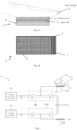
- FIG. 1A is a block diagram showing an exemplary fingerprint sensor device 1.
- the fingerprint sensor device 1 includes a sensor chip 2 disposed over a substrate carrier 4 and a protective film or cover layer 6 disposed over the sensor chip 2.
- the protective film or cover layer 6 includes an insulator or dielectric material such as glass, silicon dioxide (SiO 2 ), sapphire, plastic, polymer, other substantially similar materials.
- the protective film or cover layer 6 is configured to protect the sensor chip 2 and potentially function as a part of a dielectric layer between a surface of a finger 8 and conductive sensing electrodes of individual sensor pixels in the sensor chip 2.
- the protective film or cover layer 6 is an optional layer depending on the application of the fingerprint sensor device 1.
- the fingerprint sensor device 1 can be disposed through an opening of a top cover glass of an electronic device such as a mobile phone or under a top cover glass of the electronic device.
- the protective film or cover 6 is not needed because the top cover glass of the electronic device will function to protect the sensor chip 2 and act as the dielectric layer.
- the sensor chip 2 includes an array of sensor pixels that in combination senses or captures fingerprint data from the finger 8 in contact with the protective film or cover layer 6.
- Each sensor pixel of the sensor chip 2 generates an output signal (e.g., a voltage) based on a capacitance of a capacitor associated with a ridge or valley of the finger 8.
- the output signals when combined represents a fingerprint image of the finger 8. Higher the number of pixel sensors, greater the resolution of the fingerprint image.
- FIG. 1B is a diagram showing an exemplary sensor chip 2.
- the sensor chip 2 includes a pixelated sensor array 3 which occupies a significant portion of the sensor chip 2.
- Each sensor pixel in the pixelated sensing element array 3 includes a CMOS capacitive sensor or other types of sensors that can sense fingerprint features.
- the sensor chip 2 includes a signal processing unit 5 for processing signals received from all of the sensor pixels in the pixelated sensor array 3, and a connection unit 7 electrically coupled to the signal processing unit 5.
- the signal processing unit 5 includes various signal processing components including amplifiers, filters, and an analog to digital converter (ADC).
- the connection unit 7 includes multiple electrodes which can be connected to external circuitry through wire-bonding, bump bonding or other connection means.
- the connection unit 7 can be disposed along an edge of the sensor chip 2 for the convenience of interfacing with other components of the fingerprint sensor device 1.
- the array 3 of sensor pixels in the sensor chip 2 can be arranged to have various shapes and sizes.
- the array 3 of sensor pixels may be arranged to have a rectangular shape with a width of the rectangular shape being larger than a height of the rectangular shape.
- Exemplary sizes for the rectangular shaped sensor chip include 24 ⁇ 88, 32 ⁇ 88, 56 ⁇ 88 sensor pixels.
- the array 3 of sensor pixels in the sensor chip 2 may be arranged to have a square shape.
- Exemplary sizes for the square shaped sensor chip 2 include 32 ⁇ 32, 64 ⁇ 64, 96 ⁇ 96 and 128 ⁇ 128 sensor pixels.
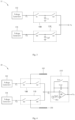
- FIG. 2 is a schematic diagram of an exemplary sensor pixel circuitry 10 according to an embodiment of the disclosed technology.
- the sensor pixel circuitry 10 corresponds to at least part of the structure within each sensor pixel in the array 3 of sensor pixels.
- the sensor pixel circuitry 10 includes a capacitive sensing layer 100, a layout layer 106, voltage generators 102 and 104, and switching circuitry such as switching networks 108 and 110.
- the circuitry of switching networks 108 and 110 can be implemented using sample-and-hold circuitry.
- the capacitive sensing layer 100 can be a conductive layer or electrode layer and can be implemented as one of the opposing sensor plates or electrodes in a capacitor.
- the capacitive sensing layer 100 and the surface of the finger form the two opposing plates of a capacitor.
- the capacitive sensing layer 100 includes a metal layer within an integrated circuitry (IC) layout, which forms a capacitor C1 with a ground terminal.
- IC integrated circuitry
- a passivation layer (not illustrated in FIG. 1 ) is usually disposed to cover the capacitive sensing layer 100, for receiving a touch of a user.
- the passivation layer may be the protective film or cover layer 6 shown in FIG 1A .
- the passivation layer is a top cover glass of an electronic device that function to protect the sensor chip 2 and act as the dielectric layer.
- the passivation layer includes insulating materials such as a glass, a sapphire, a plastic or a polymer, etc.
- the layout layer 106 may be a poly layer of conductive (e.g., metal) layers utilized for IC layout.
- the layout layer 106 forms a capacitor Cp2 with a signal ground terminal.
- the signal ground terminal is not limited to a system ground terminal with 0 voltage.
- a terminal or a layout layer receiving a fixed voltage is considered as a signal ground terminal.
- the capacitor Cp2 may be a parasitic capacitor between the layout layer 106 and another layout layer, or include a capacitor coupled between the layout layer 106 and the signal ground terminal.
- the voltage generators 102 and 104 are configured to generate drive voltages V1 and V2.
- the switching network 108 includes switches S1 and S2.
- the switches S1 and S2 are connected in series, and the capacitive sensing layer 100 is electrically coupled between the switches S1 and S2.
- the switching network 110 includes switches S3 and S4.
- the switches S3 and S4 are connected in series, and the layout layer 106 is electrically coupled between the switches S3 and S4.
- the switches S1 and S2 can be controlled by a clock signal or other control signals, such that the switching network 108 turns on an electrical connection between the voltage generator 102 and the capacitive sensing layer 100 by switching on the switch S1 and turns off an electrical connection between the capacitive sensing layer 100 and the output terminal N by switching off the switch S2 during a first period.
- the switching network 108 turns off the electrical connection between the voltage generator 102 and the capacitive sensing layer 100 by switching off the switch S1 and turns on the electrical connection between the capacitive sensing layer 100 and the output terminal N by switching on the switch S2.
- switch S1 operates as a charging switch
- switch S2 operates as a charge sensing switch to synchronously charge and sense capacitor C1 associated with the capacitive sensing layer 100 during respective time periods.
- the switches S3 and S4 can be controlled by a clock signal or other control signals, such that the switching network 110 turns on an electrical connection between the voltage generator 104 and the layout layer 106 by switching on switch S3 and turns off an electrical connection between the layout layer 106 and the output terminal N by switching off switch S4 during the first period.
- the switching network 110 turns off the electrical connection between the voltage generator 104 and the layout layer 106 by switching off switch S3 and turns on the electrical connection between the layout layer 106 and the output terminal N by switching on switch S4.
- switch S3 operates as a charging switch
- switch S4 operates as a charge sensing switch to synchronously charge and sense capacitor Cp2 associated with the integrated circuit layout layer 106 during respective time periods.
- the switching networks 108 and 110 can adequately charge the capacitors C1 and Cp2 using the voltage generators 102 and 104, and output the charging result through the output terminal N to enhance an accuracy of fingerprint identification.
- the voltage generators 102 and 104 can vary the voltages generated V1 and V2 to enhance the accuracy of fingerprint identification.
- the capacitor C1 formed between the capacitive sensing layer 100 and the ground terminal includes a parasitic capacitor Cp1 formed between the capacitive sensing layer 100 and the ground terminal, and a touch sensing capacitor Cf formed when the user's finger (e.g., a ridge of the finger) is touching the passivation layer over the capacitive sensing layer 100.
- the capacitance value of the touch sensing capacitor Cf is substantially 0, and when the user's finger touches the passivation layer over the capacitive sensing layer 100, the touching capacitor Cf has a nonzero capacitance value that depends on the spacing from the capacitive sensing layer 100. Therefore, the capacitance value of the capacitor C1 varies according to whether the user's finger touches the passivation layer over the capacitive sensing layer 100 and the local spacing between a location on the touched part of the finger and the layer 100.
- the capacitance value of the touch sensing capacitor Cf varies from one part of the finger to another part according to a distance between the portion of the finger (e.g., a ridge of the finger) touching the passivation layer over the capacitive sensing layer 100 and the capacitive sensing layer 100.
- This variation in the touch sensing capacitor Cf is captured by the array of sensor pixels and the output of the array of sensor pixels provides a map representing the surface profile of the touched portion of the finger and thus can be used to reconstruct the fingerprint pattern.
- This reconstruction based on the spatial variation in the touch sensing capacitor Cf can be achieved by the subsequent signal processing circuitry.
- a fingerprint identification system that implements structures and functions substantially equivalent to the sensor chip 2 in FIG. 1B includes a signal processing unit (e.g., substantially similar to the signal processing unit 5 of the sensor chip 2) in communication with the sensor pixel circuitry (e.g., substantially similar to the array 3 of sensor pixels) can sense the capacitance variation of the touch sensing capacitor Cf, and determine a location of the capacitive sensing layer 100 corresponds to a ridge or valley of the finger touching the passivation layer over the capacitive sensing layer 100.
- a signal processing unit e.g., substantially similar to the signal processing unit 5 of the sensor chip 2
- the sensor pixel circuitry e.g., substantially similar to the array 3 of sensor pixels
- FIG. 3 is a circuit diagram showing an exemplary circuit equivalent of the sensor pixel circuitry 10.
- the switches S1 through S4 are controlled by a clock signal to control the on-off states of the switches.
- the switches S2 and S4 are turned off when the switches S1 and S3 are turned on, and the switches S2 and S4 are turned on when the switches S1 and S3 are turned off.
- voltage V1 charges capacitor C1
- voltage V2 charges capacitor Cp2.
- the capacitor C1 exchanges electric charges with capacitor Cp2 to form a resulting voltage Vr at the output terminal N.
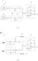
- FIG. 4 is a schematic diagram of an exemplary sensor pixel circuitry 30 according to an embodiment of the disclosed technology.
- FIG. 5 is a schematic diagram of an equivalent circuitry of the sensor pixel circuitry 30.
- the sensor pixel circuitry 30 is substantially similar to the sensor pixel circuitry 10. Different from the sensor pixel circuitry 10, the sensor pixel circuitry 30 includes an integrator INT electrically coupled to the output terminal N, for storing the electric charges V1*Cf caused by ridges and valleys touching the passivation layer over the capacitance sensing layer100.
- the inclusion of the integrator INT enhances the signal-to-noise ratio (SNR).
- the integrator INT includes a reference voltage generator 300, an amplifier OP, an integrating capacitor Cint and a reset switch Srst.
- the reference voltage generator 300 is configured to generate a reference voltage Vref.
- the amplifier OP includes a positive input terminal electrically coupled to the reference voltage generator 300 for receiving the reference voltage Vref, a negative input terminal electrically coupled to the output terminal N for receiving the resulting voltage Vr, and an output terminal for outputting an output voltage Vo.
- the integrating capacitor Cint and the reset switch Srst are electrically coupled between the negative input terminal of the amplifier OP and the output terminal.
- a capacitance value of the parasitic capacitor Cp1 within the capacitor C1 is usually larger than a capacitance value of the touch sensing capacitor Cf, which makes it difficult to identify a variation in the capacitance of the touch sensing capacitor Cf.
- the voltage value of the reference voltage Vref received by the negative input terminal of the amplifier OP in the sensor pixel circuitry 30 can be adjusted, such that the capacitance variation of the touch sensing capacitor Cf is more prominently identified through the integrator.
- the total electric charges accumulated by the capacitor C1 and the capacitor Cp2 during the first period are larger than Vref * ( Cp1+ Cp2), and there are electric charges to be stored in the integrating capacitor Cint.
- the output voltage Vo reflects the capacitance value of the touch sensing capacitor Cf more prominently.
- the reference voltage Vref can reduce or even eliminate the effect of the parasitic capacitor Cp1 on the determination of the capacitance value of the touch sensing capacitor Cf.
- the capacitance values of the capacitors Cp1 and Cp2 may not be easily acquired.
- V1 generated by the voltage generator 102 the capacitance mismatch of the capacitors Cp1 and Cp2 due to fabrication process can be substantially eliminated.
- the capacitors Cp1 and Cp2 can be designed to have substantially equal capacitance value
- the voltage values of the voltages V1 and V2 can be adjusted to substantially eliminate the capacitance mismatch of the capacitors Cp1 and Cp2 due to fabrication.
- the sensor pixel circuitry of the disclosed technology can enhance the accuracy of fingerprint identification.
- Various modifications can be made to the above described sensor pixel circuitry (e.g., array of sensor pixels 3) and fingerprint identification system (e.g., sensor chip 2 that includes an array of sensor pixels 3 and a signal processing system 5).
- fingerprint identification system e.g., sensor chip 2 that includes an array of sensor pixels 3 and a signal processing system 5.
- DAC digital to analog converter
- the voltage generator 102 includes a DAC, which is controlled to output the voltage V1 with a variable voltage value.
- the voltage generator 104 includes a DAC, which is controlled to output the voltage V2 with a variable voltage value.
- the reference voltage generator 300 includes a DAC, which is controlled to output the reference voltage Vref with a variable voltage value.
- FIG. 6 is a schematic diagram of an exemplary sensor pixel circuitry 60 according to an embodiment of the disclosed technology.
- the sensor pixel circuitry 60 can be substantially similar to the sensor pixel circuitry 30.
- the sensor pixel circuitry 60 utilizes electric charge supplying modules 602 and 604 to function as the voltage generators 102 and 104 of the sensor pixel circuitry 30 in FIGS. 2 , 3 4 and 5 .
- the electric charge supplying module 602 is electrically coupled between the switch S2 and the capacitive sensing layer 100.
- the electric charge supplying module 604 is electrically coupled between the switch S4 and the layout layer 106.
- the electric charge supplying module 602 includes the switches S11 and S12 electrically coupled to a voltage V+ and a voltage V - , respectively.
- the electric charge supplying module 604 includes the switches S31 and S32 electrically coupled to a voltage V+ and a voltage V - , respectively.
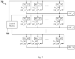
- FIGS. 7 through 8 illustrate exemplary embodiments of a fingerprint identification system using an exemplary sensor pixel array arrangement to detect a presence of a ridge or valley of a finger at a specific location of the single sensor pixel circuitry.
- Proper arrangement of the sensor pixel circuitry in a fingerprint identification system can assist in identification of a user's fingerprint.
- FIG. 7 is a schematic diagram of an exemplary fingerprint identification system 70.
- the fingerprint identification system 70 is an implementation of the sensor chip 2 that combines the structures and functions of the array 3 of sensor pixels in electrical communication with the signal processing system 5 as shown in FIG 1B .
- the fingerprint identification system includes an array of sensor pixel circuitry Pix_11 through Pix_MN, corresponding enable switches SW_11 through SW_MN, corresponding analog to digital converters ADC_1 through ADC_M and a control module 700.
- the sensor pixel circuitry Pix_11 through Pix_MN are arranged in an exemplary array configuration.
- the array of sensor pixel circuitry Pix_11 through Pix_MN are arranged in M rows and N columns.
- Each sensor pixel circuitry corresponds to and electrically coupled to an enable switch, and a row of sensor pixel circuitry correspond to and electrically coupled to an analog to digital converter.
- the group (e.g., row or column) of sensor pixel circuitry Pix_11 through Pix_1N are electrically coupled to the analog to a corresponding digital converter ADC_1.
- the group of sensor pixel circuitry Pix_21 through Pix_2N are electrically coupled to the analog to digital converter ADC_2.
- Remaining groups of sensor pixel circuitry can be similarly electrically coupled to corresponding analog to digital converters.
- the array of sensor pixel circuitry Pix_11 through Pix_MN and the enable switches SW_11 through SW_MN are electrically coupled to the control module 700 for receiving control signals generated by the control module 700.
- Each sensor pixel circuitry of the array of sensor pixel circuitry Pix_11 through Pix_MN can be substantially similar to the sensor pixel circuitry 30 or 60 or any other configurations described in this patent document.
- output voltages Vo_11 through Vo_MN are outputted by the integrators of the sensor pixel circuitry Pix_11 through Pix_MN.
- multiple sensor pixel circuitry can share one integrator for various potential advantages including to save layout space and to simplify the design, for example.
- the operational principles and detail operations of each sensor pixel circuitry in the array of sensor pixel circuitry Pix_11 through Pix_MN can be substantially similar to the description of the sensor pixel circuitry 30 or 60 or any other configurations described in this patent document.
- the control module 700 controls the enable switches SW_11 through SW_MN, such that a conducting period of an enable switch corresponding to a given sensor pixel circuitry in the array of sensor pixel circuitry (e.g., Pix_11 through Pix_MN) and a conducting period of an enable switch corresponding to another sensor pixel circuitry of the same row of sensor pixel circuitry (e.g., Pix_11 through Pix_MN) can differ in time.
- the control module 700 selectively turns on and off the switches SW_11 through SW_MN to selectively vary the conducting period of the different sensor pixel circuitry in the same row (e.g., Pix_11 through Pix_MN) for readout by ADC.
- the control module 700 is configured to control the sensor pixel circuitry for the other rows in a similar manner.
- the control module 700 is configured to turn on the enable switches of the array of sensor pixel circuitry substantially in parallel.
- the control module 700 can enable SW11 through SWMN at substantially the same time, so that ADC 1-M are configured to readout data in parallel.
- the control module 700 is configured to scan through one or more lines (e.g., rows, columns, or other groups) at a time to readout all of the pixel output voltage.
- FIG. 8 illustrates examples of waveforms of various signals associated with a fingerprint identification system.
- the example waves shown in FIG. 8 are associated with row M of the rows of sensor pixel circuitry in FIG. 7 .
- An output of an integrator (e.g., integrator INT) is represented by the output voltage Vo_m1.
- the control signal of the enable switch SW_m1 pulls high at a time t1 for a time period, and the output voltage Vo_m1 is delivered to the analog to digital converter ADC_m through the enable switch SW_m1.
- the control signal of the reset switch Srst pulls high at a time tr1, such that the integrating capacitor Cint of the sensor pixel circuitry Pix_m1 is return to zero, so as to be ready for performing another integration for a next time period.
- the integrator of the sensor pixel circuitry Pix_m2 also performs integration substantially simultaneously.
- the control signal of the enable switch SW_m2 pulls high at a time t2 for a time period, and the output voltage Vo_m2 is delivered to the analog to digital converter ADC_m through the enable switch SW_m2.
- the time t2 is at some time after t1.
- each of the sensor pixel circuitry Pix_m3 through Pix_mN is configured to deliver the output voltages to the corresponding analog to digital converter ADC_m at different after time t2.
- the different time instances for sensor pixel circuitry Pix_m1 through Pix_mN may be non-overlapping time instances.
- the analog to digital converter ADC_m receives the output voltage of each sensor pixel circuitry in the row of the sensor pixel circuitry Pix_m1 through Pix_mN.
- Each sensor pixel circuitry within the array of sensor pixel circuitry Pix_11 through Pix_MN includes a dedicated integrator. As such, the integration processes of the different sensor pixel circuitry in a given row of sensor pixel circuitry (e.g., Pix_m1 through Pix_mN) can be performed in parallel by the multiple integrators. With a fixed integration period for each integrator, the fingerprint identification system 70 can shorten an overall integration period for the array of sensor pixel circuitry.
- the overall integration period for a row of sensor pixel circuitry can be fixed (e.g., at a period longer than individual sensor pixel circuitry integration period) to allow a longer integration period for each sensor pixel circuitry in the rows of sensor pixel circuitry Pix_m1 through Pix_mn. Because the individual integration processes can be performed in parallel for all pixel sensor circuitry, the overall integration period can be reduced even when the individual integration period is increased. Increasing the individual integration period, while reducing the overall integration period, can allow the noise to be sufficiently averaged, and the SNR of the sensor pixel circuitry can be further enhanced. Because each pixel integrator can act as a pixel level signal (voltage) storage, and the stored signal can be readout later by a scan readout process using the ADCs and control module, for example.
- a selected subset or the entire array of sensor pixel circuitry can be enabled to integrate the selected subset or the entire array of sensor pixel circuitry.
- the integrating capacitor connected to the negative feedback path of each integrator can be used as a local memory to store the charges associated with the corresponding sensor pixel. Readout of the sensor pixel data can be performed per selected group or subset of the array of senor pixel circuitry, such as each row, column, etc.
- Readout process is a relatively quick compared to the integration process, and thus, parallel integration of the selected subset or the entire array of sensor pixel circuitry while the finger is touching the fingerprint identification system (e.g., the passivation layer over the sensor pixel circuitry) can be advantageous by not wasting the sensor pixel circuitry under the finger touch.
- the fingerprint identification system e.g., the passivation layer over the sensor pixel circuitry
- the fingerprint identification system can apply an excitation signal directly to a finger via an electrode to increase a voltage difference between two terminals of the touch sensing capacitor Cf, such that more electric charges are accumulated in the touch sensing capacitor Cf during the first period.
- the fingerprint identification system can apply a high voltage to the finger during the second period, such that more electric charges are stored in the integrating capacitor Cint.
- FIG. 9 is a schematic diagram of an exemplary sensor pixel circuitry 90 and an external electrode Et.
- the sensor pixel circuitry 90 can be substantially similar to the sensor pixel circuitry 30 or 60.
- the switches S1 and S3 are controlled by the clock signal ck1, and the switches S2 and S4 are controlled by the clock signal ck2.
- the clock signal ck1 is high, the switches S1 and S3 are turned on.
- the clock signal ck1 is low, the switches S1 and S3 are turned off.
- the clock signal ck2 is high, the switches S2 and S4 are turned on.
- the switches S2 and S4 are turned off
- the external electrode Et can be electrically connected to the clock signal ck2, so as to pull high the voltage applied to the user's finger through the external electrode Et during the second period (i.e., the period when the switches S2 and S4 are turned on and the switches S1 and S3 are turned off).
- the second period i.e., the period when the switches S2 and S4 are turned on and the switches S1 and S3 are turned off.
- FIG. 10 is a schematic diagram illustrating exemplary waveforms of clock signals ck1 and ck2.
- the clock signals ck1 and ck2 are inverted and out of phase with each other.
- ck1 is set high
- ck2 is set low.
- a row of sensor pixel circuitry (e.g., Pix_m1 through Pix_mN) are couple to a corresponding analog to digital converter (e.g., ADC_m).
- the sensor pixel circuitry units can be divided into different groups of sensor pixel circuitry. All sensor pixel circuitry in a given group can be electrically coupled to the same corresponding analog to digital converter.
- the groups of sensor pixel circuitry can be determined using rows, columns, a predetermined number of sensor pixel circuitry, a particular shape (e.g., a square) or other groupings that allow an enable switch corresponding to a sensor pixel circuitry in one group to have a different conducting period than another enable switch corresponding to a sensor pixel circuitry in a different group.
- a particular shape e.g., a square
- FIGS. 11, 12 and 13 Additional examples of modifications to the sensor pixel circuitry are shown FIGS. 11, 12 and 13 .
- FIG. 11 is a diagram showing another exemplary sensor pixel circuitry 1100 for compensating for capacitor mismatch in a fingerprint identification system.
- the exemplary sensor pixel circuitry includes a sensor plate or a capacitive sensing layer 1102 configured to operate or function as one of two opposing conductive plates of a fingerprint associated capacitor. For example, when a finger 1108 of a user approaches the sensor plate or capacitive sensing layer 1102, a surface of the finger 1108 and the sensor plate of capacitive sensing layer 1102 configured to operate or function as the two opposing plates of capacitor Cf.
- the capacitance of the capacitor Cf can vary based at least partly on a distance between the surface of the finger (e.g., a ridge) and the sensor plate or capacitive sensing layer 1102.
- the sensor plate or capacitive sensing layer 1102 includes a conductive material, such as one of various metals.
- a voltage generator 1132 is electrically connected to the sensor plate 1102, which is electrically connected to a system ground through the surface of the finger 108. The voltage generator is configured to generate drive voltage VDD for charging the fingerprint associated capacitor Cf.
- a switching circuitry, such as a switching network 1120 includes switches 1122 and 1124 in series for being switchable in electrically connecting the sensor plate 1102 to the voltage generator 1132 and an output terminal 1140. In some implementations, the switching circuitry 1120 can be implemented using sample-and-hold circuitry.
- the switches 1122 and 1124 can be controlled by a clock signal or other control signals, such that the switching circuitry 1120 is configured to turn on an electrical connection between the voltage generator 1132 and the sensor plate 1102 by turning on the switch 1122 and turn off an electrical connection between the sensor plate 1102 and the output terminal 1140 by turning off the switch 1124 during a first period.
- the sample-and-hold circuitry 1120 is configured to turn off the electrical connection between the voltage generator 1132 and the sensor plate 1102 by turning off the switch 1122 and turn on the electrical connection between the sensor plate 1102 and the output terminal 1140 by turning on the switch 1124.
- switch 1122 operates as a charging switch
- switch 1124 operates as a charge sensing switch to synchronously charge and sense capacitor Cf associated with the sensor plate 1102 during respective time periods.
- Two substantially identical conductive layers, electrodes or plates 1104 and 1106 can be disposed below the sensor plate 1102.
- the conductive plate 1104 and the sensor plate 1102 form a corresponding capacitor CP1.
- the conductive plate 1106 and the sensor plate 1102 form a corresponding capacitor CP2.
- a switching circuitry such as a switching network 1126 includes switches 1128 and 1130 to switchable between electrically connecting the conductive plate 1104 to a voltage generator 1134 and ground 1144.
- the other conductive plate 1106 is electrically connected to ground and not electrically controlled by the switching circuitry 1126.
- the voltage generator 1134 includes a DAC1 1136 and a voltage buffer 1138 to generate and provide a variable voltage to the conductive plates 1104.
- the switching circuitry 1126 can be implemented using sample-and-hold circuitry.
- the switches 1128 and 1130 can be controlled by a clock signal or other control signals, such that the switching circuitry 1126 is configured to turn on an electrical connection between the voltage generator 1134 and the conductive plate 1104 by turning on the switch 1128 and turn off an electrical connection between the conductive plate 1104 and the ground 1144 by turning off the switch 1130 during a first period. During a second period, the switching circuitry 1126 is configured to turn off the electrical connection between the voltage generator 1134 and the conductive plate 1104 by turning off the switch 1128 and turn on the electrical connection between the conductive plate 1104 and the ground 1144 by turning on the switch 1130.
- switch 1128 operates as a charging switch
- switch 1130 operates as a grounding switch to synchronously charge and ground capacitor CP1 associated with the sensor plate 1102 during respective time periods.
- the output terminal 1140 is configured to be optionally electrically connected to an integrator 1142 for storing the electric charges caused by ridges and valleys of a finger touching the passivation layer over the sensor plate 1102.
- the inclusion of the integrator INT enhances the signal-to-noise ratio (SNR).
- the integrator includes an amplifier 1118 having a negative input electrically connected to the output terminal 1140 connected to the switching circuitry 1120.
- the amplifier 1118 has a positive input electrically connected to a reference voltage generator 1112 for receiving the reference voltage Vref.
- the reference voltage generator 1112 includes a DAC2 1114 and a voltage buffer 1116 for generating and providing a variable reference voltage.
- the amplifier 1118 includes an output terminal 114 for outputting an output voltage Vpo.
- An integrating capacitor Cint 1146 and a reset switch rst 1148 are electrically coupled in parallel between the negative input terminal of the amplifier OP 1118 and the output terminal 1144.
- the DAC1 1136 output can be set to VDD.
- the switches 1122 and 1128 are turned on and switches 1124 and 1130 are turned off.
- the charge in CP2 will be Cp2*VDD and the charge in CP1 will be 0.
- switches 1122 and 1128 are turned off and switches 1124 and 1130 are turned on.
- the charges in CP1 and CP2 will exchange.
- the charge in Cf is substantially zero, and the voltage at the negative input of the amplifier OP 1118 will be VDD/2.
- the DAC1 might be not necessary or become optional. By removing the DAC1, the DAC1 noise will no longer exist in the pixel output, which further enhances the SNR.
- FIG. 12 is a diagram showing yet another exemplary sensor pixel circuitry 1200 for compensating for capacitor mismatch in a fingerprint identification system.
- the sensor pixel circuitry 1200 is substantially similar to the sensor pixel circuitry 1100 with some variations.
- the switching circuitry 1126 is electrically connected between the conductive plate 1104 and a voltage generator 1202 that does not include a DAC.
- the output of the voltage generator 1202 preset to VDD.
- a third voltage generator 1212 is electrically connected to another switching circuitry 1204.
- the third voltage generator 1212 includes a DAC 1214 DAC1 in series with a voltage buffer 1216.
- the switching circuitry 1204 includes switches 1206 and 1208 in series for being switchable in electrically connecting a capacitor 1210 Cc between the voltage generator 1212 and a common node 1218 connecting to the sensor plate 1102 and the switching circuitry 1120 (which is switchable in electrically connecting to the output terminal 1140 and the voltage generator 1132).
- the other terminal of the capacitor 1210 Cc is electrically connected to ground. See relevant description of FIG. 11 for the circuit components of the sensor pixel circuitry 1200 that are similar to the sensor pixel circuitry 1100.
- the final voltage VPO at the output terminal 1144 without a finger touching a passivation layer over the sensor electrode 1102 during the second period is (CP1*VDD+Cc*VDAC)/(Cc+Cp1+Cp2).
- VDAC is set to VDD/2.
- VDAC is adjusted.
- FIG. 13 is a diagram showing yet another exemplary sensor pixel circuitry 1300 for compensating for capacitor mismatch in a fingerprint identification system.
- the sensor pixel circuitry 1300 is substantially similar to the sensor pixel circuitry 1200 with some variations.
- the switching circuitry 1204 includes switches 1206 and 1208 electrically connected in series for selectively electrically connecting the capacitor Cc 1210 to the voltage generator 1202 and a fourth voltage generator 1220.
- the voltage generator 1220 can be set to VDD.
- the other terminal of the capacitor Cc 1210 is electrically connected to a common node 1218 connecting to the sensor plate 1102 and the sample-and-hold circuitry 1120 (which is switchable in electrically connecting to the output terminal 1140 and the voltage generator 1132). See descriptions of FIG. 12 for the corresponding descriptions of the circuit components of the sensor pixel circuitry 1300 that are similar to the sensor pixel circuitry 1200.
- the final voltage VPO at output terminal 1144 without a finger touch during the second period Ck2 is (CP1*VDD+Cc*Vdac)/(Cc+Cp1+Cp2).
- VDAC is adjusted.
- an integrator can be shared between a number of sensor pixel circuitry units to reduce the total number of integrators in the fingerprint identification system, which provides a number potential advantages including cost reduction, layout size reduction, and simplicity in design, for example.
- Multiple units of sensor pixel circuitry share an integrator by multiplexing the output signals from a selected number of sensor pixel circuitry units into a shared integrator. For example, when grouping the array of sensor pixel circuitry units into rows, with each row assigned to an ADC, each sensor pixel circuitry unit in a row share an integrator with one or more sensor pixel circuitry units in one or more rows of sensor pixel circuitry. When grouping the sensor pixel circuitry in the array of sensor pixel circuitry into columns, each sensor pixel circuitry in a given column share an integrator with one or more sensor pixel circuitry in one or more columns.
- FIGS. 14A and 14B show examples of configurations for sharing integrators between sensor pixel circuitry units.
- FIG 14A is a diagram showing an example of a fingerprint identification system 1400 for integrator sharing between rows in an array of sensor pixel circuitry units.
- the fingerprint identification system 1400 includes a control module 1402, which is substantially similar to the control module 700 in FIG. 7 .
- An array of sensor pixel circuitry Sensor Pixel 11 through Sensor Pixel MN are grouped into rows 1 through M. Each row in the array includes N columns of sensor pixel circuitry. In the example shown in FIG. 14A , every two rows of sensor pixel circuitry share integrators. However, more than two rows of sensor pixel circuitry share integrators.
- the control module 1402 is configured to selectively enable/disable each sensor pixel circuitry in the array by turning on and off corresponding enable switches SW11 through SW MN.
- the switch signal may be one or multiple digital logic signals.
- the control module 1402 is configured to integrate any number of sensor pixel circuitry in the array in parallel.
- the control module enables the odd row of sensor pixel circuitry (e.g., Sensor Pixel 11 through Sensor Pixel 1N) to integrate all sensor pixels in the row.
- the pixels in the odd row are configured to perform integration in parallel, and after the integration is completed, control module scans each pixels to readout their data using the ADCs.
- control module switch on the even row of sensor pixel circuitry (e.g., Sensor Pixel 21 through Sensor Pixel 2N), which shares the integrators used by the odd row of sensor pixel circuitry (e.g., Sensor Pixel 11 through Sensor Pixel 1N) to perform integration in parallel.
- All of the odd and even rows can be processed in similar manner. In some implementations, all odd rows can be processed at substantially the same time in parallel. Then all of the even rows can be processed at substantially the same time in parallel. In some implementations, any number of odd and even rows can be processed together in parallel. In addition, the even rows can be processed first in some implementations. Thus, the order of the even and odd rows is not limiting.
- FIG 14B is a diagram showing an exemplary fingerprint identification system 1410 for integrator sharing between columns in an array of sensor pixel circuitry.
- the fingerprint identification system 1410 includes a control module 1402, which can be substantially similar to the control module 700 in FIG. 7 .
- An array of sensor pixel circuitry Sensor Pixel 11 through Sensor Pixel 4N are grouped into columns 1 through 4. While more than 4 columns is included in an array, only 4 columns are shown in FIG. 14B for illustrative purposes.
- Each column in the array includes N rows of sensor pixel circuitry. In the example shown in FIG. 14B , every two columns of sensor pixel circuitry share integrators. However, more than two columns of sensor pixel circuitry share integrators.
- the control module 1402 is configured to selectively enable/disable each sensor pixel circuitry in the array by turning on and off corresponding enable switches SW11 through SW 4N. By controlling the appropriate sensor pixel circuitry through the enable switches, the control module 1402 is configured to integrate any number of sensor pixel circuitry in the array in parallel. In the example shown in FIG. 14B , the control module enables the odd column of sensor pixel circuitry (e.g., Sensor Pixel 11 through Sensor Pixel 1N) to integrate all sensor pixels in the odd column. The sensor pixels in the odd column are configured to perform integration in parallel, and after the integration completed, control module is configured to scan each sensor pixel to readout the data using the ADCs.
- the control module enables the odd column of sensor pixel circuitry (e.g., Sensor Pixel 11 through Sensor Pixel 1N) to integrate all sensor pixels in the odd column.
- the sensor pixels in the odd column are configured to perform integration in parallel, and after the integration completed, control module is configured to scan each sensor pixel to readout the data using the ADCs.
- the control module is configured to switch on the even column of sensor pixel circuitry (e.g., Sensor Pixel 21 through Sensor Pixel 2N), which shares the integrators used by the odd column of sensor pixel circuitry (e.g., Sensor Pixel 11 through Sensor Pixel 1N) to perform integration in parallel.
- All of the odd and even columns can be processed in similar manner. In some implementations, all odd columns can be processed at substantially the same time in parallel. Then all of the even columns can be processed at substantially the same time in parallel. In some implementations, any number of odd and even columns can be processed together in parallel. In addition, the even columns can be processed first in some implementations. Thus, the order of the even and odd columns is not limiting.
- the array of sensor pixels can be grouped in a way different than rows or columns and the integrator sharing can be implemented in various ways depending on the grouping of the array of sensor pixels.
- FIG. 14C is a diagram showing an exemplary sensor pixel circuitry and fingerprint identification system 1420 with two sensor pixel circuitry sharing an integrator.
- the fingerprint identification system 1420 shows a simple example where two sensor pixel circuitry 1422 and 1424 share one integrator 1426.
- the sensor pixel circuitry 1422 and 1424 can be substantially similar to sensor pixel circuitry 10 in FIG. 2 or any other configurations described in this patent document.
- FIG. 14D is a diagram showing an exemplary sensor pixel circuitry and fingerprint identification system 1430 with two sensor pixel circuitry sharing an integrator.
- the fingerprint identification system 1430 shows a simple example where two sensor pixel circuitry 1432 and 1434 share one integrator 1436.
- the sensor pixel circuitry 1422 and 1424 can be substantially similar to sensor pixel circuitry in FIGS. 11, 12 and 13 or any other configurations described in this patent document.
- FIGS. 14A , 14B , 14C and 14D some of the components including the ADC are not included in the figures for illustrative purposes only.
- the disclosed technology utilizes integrators for storing the electric charges accumulated by the touch sensing capacitor, utilizes the voltage generator for outputting the variable voltage and adjusting the electric charges stored in the parasitic capacitors, and utilizes the sensor pixel circuitry with a dedicated integrator for performing integration across a group of sensor pixel circuitry in parallel to enhance the SNR.
- the sensor pixel circuitry and the fingerprint identification system described in this patent document provide accurate fingerprint identification even without a metal ring.
Landscapes
- Engineering & Computer Science (AREA)
- Human Computer Interaction (AREA)
- Physics & Mathematics (AREA)
- General Physics & Mathematics (AREA)
- Multimedia (AREA)
- Theoretical Computer Science (AREA)
- Measurement Of The Respiration, Hearing Ability, Form, And Blood Characteristics Of Living Organisms (AREA)
- Image Input (AREA)
- Measurement Of Length, Angles, Or The Like Using Electric Or Magnetic Means (AREA)
Description
- This patent document relates to sensor pixel circuitry and fingerprint identification.
- Various electronic devices or information systems can employ user authentication mechanisms to protect personal data and prevent unauthorized access. User authentication on an electronic device or information system can be carried out through one or multiple forms of personal identification and authentication methods, including one or more biometric identifiers. A biometric identifier can be used alone or in addition to a conventional authentication method, such as a password authentication method. A popular form of biometric identifiers is a person's fingerprint pattern. A fingerprint sensor can be built into the electronic device to read a user's fingerprint pattern so that the device can only be unlocked by an authorized user of the device through authentication of the authorized user's fingerprint pattern. In some implementations, such as fingerprint sensor includes sensor pixel circuitry with pixelated pixel sensor elements for capturing fingerprint patterns for user identification.
- Capacitive fingerprint identification devices and systems sense capacitance variations to determine ridges and valleys of a user's finger. A low signal-to-noise ratio (SNR), when present in the capacitive fingerprint identification system, lowers the accuracy of fingerprint identification. According to
US7864992 or toUS6088471 , one technique for increasing the SNR uses a metal ring to transmit an excitation signal directly to the finger to be identified to enhance the identification accuracy. The metal ring occupies valuable space on a semiconductor layout for the device, which increases product cost and affect appearances of products. - Lee, Jeong-Woo, et al. "A 600-dpi capacitive fingerprint sensor chip and image-synthesis technique." IEEE Journal of Solid-State Circuits 34.4 (1999): 469-475, disclosed using a shielding metal plate below the sensing plate to shield the fringe capacitances between the sensing plate and the substrate.
- This patent document describes technology for providing devices, systems, and techniques to perform fingerprint detection in electronic devices including portable or mobile computing devices, such as laptops, tablets, smartphones, and gaming systems.
- The technologies described in this patent document can provide sensor pixel circuitry and a fingerprint identification system for accurate fingerprint identification without using a metal ring.
- The present invention is defined by
claim 1. -
-
FIG. 1A is a block diagram showing an exemplary fingerprint sensor device. -
FIG. 1B is a diagram showing an exemplary sensor chip. -
FIG. 2 is a schematic diagram of exemplary sensor pixel circuitry. -
FIG. 3 is a schematic diagram of an equivalent circuitry of the sensor pixel circuitry inFIG. 1 . -
FIG. 4 is a schematic diagram of exemplary sensor pixel circuitry with in-pixel integrator. -
FIG. 5 is a schematic diagram of an equivalent circuitry of the sensor pixel circuitry inFIG. 4 . -
FIG. 6 is a schematic diagram of an exemplary sensor pixel circuitry. -
FIG. 7 is a schematic diagram of an exemplary fingerprint identification system. -
FIG. 8 is a schematic diagram illustrating exemplary waveforms of associated signals. -
FIG. 9 is a schematic diagram of exemplary sensor pixel circuitry and an external electrode according to an embodiment of the present invention. -
FIG. 10 is a schematic diagram illustrating waveforms of clock signals according to an embodiment of the present invention. -
FIG. 11 is a schematic diagram illustrating yet another exemplary sensor pixel circuitry to compensate for capacitor mismatch in a fingerprint identification system. -
FIG. 12 is a schematic diagram illustrating yet another exemplary sensor pixel circuitry to compensate for capacitor mismatch in a fingerprint identification system. -
FIG. 13 is a schematic diagram illustrating yet another exemplary sensor pixel circuitry to compensate for capacitor mismatch in a fingerprint identification system. -
FIG. 14A is a schematic diagram illustrating an exemplary fingerprint identification system for sharing integrators between sensor pixel circuitry. -
FIG. 14B is a schematic diagram illustrating another exemplary fingerprint identification system for sharing integrators between sensor pixel circuitry. -
FIG. 14C is a schematic diagram illustrating an exemplary fingerprint identification system for sharing integrators between two sensor pixel circuitry. -
FIG. 14D is a schematic diagram illustrating an exemplary fingerprint identification system for sharing integrators between two sensor pixel circuitry. -
FIG. 1A is a block diagram showing an exemplaryfingerprint sensor device 1. Thefingerprint sensor device 1 includes asensor chip 2 disposed over asubstrate carrier 4 and a protective film orcover layer 6 disposed over thesensor chip 2. The protective film orcover layer 6 includes an insulator or dielectric material such as glass, silicon dioxide (SiO2), sapphire, plastic, polymer, other substantially similar materials. The protective film orcover layer 6 is configured to protect thesensor chip 2 and potentially function as a part of a dielectric layer between a surface of afinger 8 and conductive sensing electrodes of individual sensor pixels in thesensor chip 2. The protective film orcover layer 6 is an optional layer depending on the application of thefingerprint sensor device 1. Thefingerprint sensor device 1 can be disposed through an opening of a top cover glass of an electronic device such as a mobile phone or under a top cover glass of the electronic device. When used in the under-the-glass application, the protective film orcover 6 is not needed because the top cover glass of the electronic device will function to protect thesensor chip 2 and act as the dielectric layer. Thesensor chip 2 includes an array of sensor pixels that in combination senses or captures fingerprint data from thefinger 8 in contact with the protective film orcover layer 6. Each sensor pixel of thesensor chip 2 generates an output signal (e.g., a voltage) based on a capacitance of a capacitor associated with a ridge or valley of thefinger 8. The output signals when combined represents a fingerprint image of thefinger 8. Higher the number of pixel sensors, greater the resolution of the fingerprint image. -
FIG. 1B is a diagram showing anexemplary sensor chip 2. The sensor chip 2includes apixelated sensor array 3 which occupies a significant portion of thesensor chip 2. Each sensor pixel in the pixelatedsensing element array 3 includes a CMOS capacitive sensor or other types of sensors that can sense fingerprint features. The sensor chip 2includes asignal processing unit 5 for processing signals received from all of the sensor pixels in thepixelated sensor array 3, and aconnection unit 7 electrically coupled to thesignal processing unit 5. The signal processing unit 5includes various signal processing components including amplifiers, filters, and an analog to digital converter (ADC). The connection unit 7includes multiple electrodes which can be connected to external circuitry through wire-bonding, bump bonding or other connection means. Theconnection unit 7 can be disposed along an edge of thesensor chip 2 for the convenience of interfacing with other components of thefingerprint sensor device 1. - The
array 3 of sensor pixels in thesensor chip 2 can be arranged to have various shapes and sizes. For example, thearray 3 of sensor pixels may be arranged to have a rectangular shape with a width of the rectangular shape being larger than a height of the rectangular shape. Exemplary sizes for the rectangular shaped sensor chip include 24 × 88, 32 × 88, 56 × 88 sensor pixels. In some implementations, thearray 3 of sensor pixels in the sensor chip 2may be arranged to have a square shape. Exemplary sizes for the square shapedsensor chip 2 include 32 × 32, 64 × 64, 96 × 96 and 128 × 128 sensor pixels. -
FIG. 2 is a schematic diagram of an exemplarysensor pixel circuitry 10 according to an embodiment of the disclosed technology. Thesensor pixel circuitry 10 corresponds to at least part of the structure within each sensor pixel in thearray 3 of sensor pixels. Thesensor pixel circuitry 10 includes acapacitive sensing layer 100, alayout layer 106,voltage generators networks networks capacitive sensing layer 100 can be a conductive layer or electrode layer and can be implemented as one of the opposing sensor plates or electrodes in a capacitor. When disposed opposite to a surface of the finger, thecapacitive sensing layer 100 and the surface of the finger (e.g., a ridge or a valley of the finger) form the two opposing plates of a capacitor. The capacitive sensing layer 100includes a metal layer within an integrated circuitry (IC) layout, which forms a capacitor C1 with a ground terminal. Over thecapacitive sensing layer 100, a passivation layer (not illustrated inFIG. 1 ) is usually disposed to cover thecapacitive sensing layer 100, for receiving a touch of a user. The passivation layer may be the protective film orcover layer 6 shown inFIG 1A . In some implementations, e.g., under the glass configuration, the passivation layer is a top cover glass of an electronic device that function to protect thesensor chip 2 and act as the dielectric layer. The passivation layer includes insulating materials such as a glass, a sapphire, a plastic or a polymer, etc. - When a finger of the user approaches the
capacitive sensing layer 100, a capacitance value of the capacitor C1 varies accordingly. The layout layer 106may be a poly layer of conductive (e.g., metal) layers utilized for IC layout. Thelayout layer 106 forms a capacitor Cp2 with a signal ground terminal. The signal ground terminal is not limited to a system ground terminal with 0 voltage. A terminal or a layout layer receiving a fixed voltage is considered as a signal ground terminal. The capacitor Cp2may be a parasitic capacitor between thelayout layer 106 and another layout layer, or include a capacitor coupled between thelayout layer 106 and the signal ground terminal. Thevoltage generators switching network 108 includes switches S1 and S2. The switches S1 and S2 are connected in series, and thecapacitive sensing layer 100 is electrically coupled between the switches S1 and S2. Theswitching network 110 includes switches S3 and S4. The switches S3 and S4 are connected in series, and thelayout layer 106 is electrically coupled between the switches S3 and S4. - The switches S1 and S2 can be controlled by a clock signal or other control signals, such that the
switching network 108 turns on an electrical connection between thevoltage generator 102 and thecapacitive sensing layer 100 by switching on the switch S1 and turns off an electrical connection between thecapacitive sensing layer 100 and the output terminal N by switching off the switch S2 during a first period. During a second period, theswitching network 108 turns off the electrical connection between thevoltage generator 102 and thecapacitive sensing layer 100 by switching off the switch S1 and turns on the electrical connection between thecapacitive sensing layer 100 and the output terminal N by switching on the switch S2. Thus, switch S1 operates as a charging switch and switch S2 operates as a charge sensing switch to synchronously charge and sense capacitor C1 associated with thecapacitive sensing layer 100 during respective time periods. - Similarly, the switches S3 and S4 can be controlled by a clock signal or other control signals, such that the
switching network 110 turns on an electrical connection between thevoltage generator 104 and thelayout layer 106 by switching on switch S3 and turns off an electrical connection between thelayout layer 106 and the output terminal N by switching off switch S4 during the first period. During the second period, theswitching network 110 turns off the electrical connection between thevoltage generator 104 and thelayout layer 106 by switching off switch S3 and turns on the electrical connection between thelayout layer 106 and the output terminal N by switching on switch S4. Thus, switch S3 operates as a charging switch and switch S4 operates as a charge sensing switch to synchronously charge and sense capacitor Cp2 associated with the integratedcircuit layout layer 106 during respective time periods. - The switching
networks voltage generators voltage generators - For example, the capacitor C1 formed between the
capacitive sensing layer 100 and the ground terminal includes a parasitic capacitor Cp1 formed between thecapacitive sensing layer 100 and the ground terminal, and a touch sensing capacitor Cf formed when the user's finger (e.g., a ridge of the finger) is touching the passivation layer over thecapacitive sensing layer 100. The capacitor C1 represents an equivalent capacitor between thecapacitive sensing layer 100 and the ground terminal, which is a combination of the parasitic capacitor Cp1 and the touch sensing capacitor Cf connected in parallel (i.e., C1=Cp1+Cf). When the user's finger is not in contact with the passivation layer over thecapacitive sensing layer 100, the capacitance value of the touch sensing capacitor Cf is substantially 0, and when the user's finger touches the passivation layer over thecapacitive sensing layer 100, the touching capacitor Cf has a nonzero capacitance value that depends on the spacing from thecapacitive sensing layer 100. Therefore, the capacitance value of the capacitor C1 varies according to whether the user's finger touches the passivation layer over thecapacitive sensing layer 100 and the local spacing between a location on the touched part of the finger and thelayer 100. When the finger of the user touches the passivation layer over thecapacitive sensing layer 100, the capacitance value of the touch sensing capacitor Cf varies from one part of the finger to another part according to a distance between the portion of the finger (e.g., a ridge of the finger) touching the passivation layer over thecapacitive sensing layer 100 and thecapacitive sensing layer 100. This variation in the touch sensing capacitor Cf is captured by the array of sensor pixels and the output of the array of sensor pixels provides a map representing the surface profile of the touched portion of the finger and thus can be used to reconstruct the fingerprint pattern. This reconstruction based on the spatial variation in the touch sensing capacitor Cf can be achieved by the subsequent signal processing circuitry. A fingerprint identification system that implements structures and functions substantially equivalent to thesensor chip 2 inFIG. 1B includes a signal processing unit (e.g., substantially similar to thesignal processing unit 5 of the sensor chip 2) in communication with the sensor pixel circuitry (e.g., substantially similar to thearray 3 of sensor pixels) can sense the capacitance variation of the touch sensing capacitor Cf, and determine a location of thecapacitive sensing layer 100 corresponds to a ridge or valley of the finger touching the passivation layer over thecapacitive sensing layer 100. -
FIG. 3 is a circuit diagram showing an exemplary circuit equivalent of thesensor pixel circuitry 10. The switches S1 through S4 are controlled by a clock signal to control the on-off states of the switches. The switches S2 and S4 are turned off when the switches S1 and S3 are turned on, and the switches S2 and S4 are turned on when the switches S1 and S3 are turned off. During the first period when switches S1 and S3 are turned on and switches S2 and S4 are turned off, voltage V1 charges capacitor C1, and voltage V2 charges capacitor Cp2. During the second period when switches S1 and S3 are turned off and switches S2 and S4 are turned on, the capacitor C1 exchanges electric charges with capacitor Cp2 to form a resulting voltage Vr at the output terminal N. Moreover, a voltage value of the resulting voltage Vr can be represented using the following equations:
sensor pixel circuitry 10 is configured to output the resulting voltage Vr to a signal processing unit of a fingerprint identification system to determine whether the location of thesensor pixel circuitry 10 corresponds to a ridge or a valley of the fingerprint according to the resulting voltage Vr. -
FIG. 4 is a schematic diagram of an exemplarysensor pixel circuitry 30 according to an embodiment of the disclosed technology.FIG. 5 is a schematic diagram of an equivalent circuitry of thesensor pixel circuitry 30. Thesensor pixel circuitry 30 is substantially similar to thesensor pixel circuitry 10. Different from thesensor pixel circuitry 10, thesensor pixel circuitry 30 includes an integrator INT electrically coupled to the output terminal N, for storing the electric charges V1*Cf caused by ridges and valleys touching the passivation layer over the capacitance sensing layer100. The inclusion of the integrator INT enhances the signal-to-noise ratio (SNR). The integrator INT includes areference voltage generator 300, an amplifier OP, an integrating capacitor Cint and a reset switch Srst. Thereference voltage generator 300 is configured to generate a reference voltage Vref. The amplifier OP includes a positive input terminal electrically coupled to thereference voltage generator 300 for receiving the reference voltage Vref, a negative input terminal electrically coupled to the output terminal N for receiving the resulting voltage Vr, and an output terminal for outputting an output voltage Vo. The integrating capacitor Cint and the reset switch Srst are electrically coupled between the negative input terminal of the amplifier OP and the output terminal. - A capacitance value of the parasitic capacitor Cp1 within the capacitor C1 is usually larger than a capacitance value of the touch sensing capacitor Cf, which makes it difficult to identify a variation in the capacitance of the touch sensing capacitor Cf. The voltage value of the reference voltage Vref received by the negative input terminal of the amplifier OP in the
sensor pixel circuitry 30 can be adjusted, such that the capacitance variation of the touch sensing capacitor Cf is more prominently identified through the integrator. In some implementations, the reference voltage Vref can be set as the resulting voltage Vr in absence of a finger touch from the user (i.e., Cf=0), which is represented by
- In various circuitry designs, the capacitance values of the capacitors Cp1 and Cp2 may not be easily acquired. In some implementations, when the capacitance values of the capacitors Cp1, Cp2 are assumed to be equal, the reference voltage Vref can be set as

voltage generators reference voltage generator 300 can be adjusted to provide V1*Cp1 + V2*Cp2 = Vref * ( Cp1+ Cp2), which helps to eliminate the capacitance mismatch of the capacitors Cp1 and Cp2 caused by the fabrication process. By changing the voltage V1 generated by thevoltage generator 102, the capacitance mismatch of the capacitors Cp1 and Cp2 due to fabrication process can be substantially eliminated. - In various IC layouts, the capacitors Cp1 and Cp2 can be designed to have substantially equal capacitance value, the reference voltage Vref can be set as

- As described above, by charging the capacitors C1 and Cp2 and outputting the charging result through the output terminal N, the sensor pixel circuitry of the disclosed technology can enhance the accuracy of fingerprint identification. Various modifications can be made to the above described sensor pixel circuitry (e.g., array of sensor pixels 3) and fingerprint identification system (e.g.,
sensor chip 2 that includes an array ofsensor pixels 3 and a signal processing system 5). For example, to substantially eliminate the mismatch of the capacitors Cp1 and Cp2, at least one of the voltages V1, V2, and Vref generated by thevoltage generators reference voltage generator 300 can be adjusted. To adjust at least one of the voltages, a digital to analog converter (DAC) can be used to output a variable voltage. For example, in some implementations, the voltage generator 102includes a DAC, which is controlled to output the voltage V1 with a variable voltage value. In some implementations, the voltage generator 104includes a DAC, which is controlled to output the voltage V2 with a variable voltage value. In some implementations, the reference voltage generator 300includes a DAC, which is controlled to output the reference voltage Vref with a variable voltage value. - In addition to the DAC, a switch adjusting mechanism can be provided to generate the controllable or variable voltages V1 and V2.
FIG. 6 is a schematic diagram of an exemplarysensor pixel circuitry 60 according to an embodiment of the disclosed technology. In one implementation, thesensor pixel circuitry 60 can be substantially similar to thesensor pixel circuitry 30. Thesensor pixel circuitry 60 utilizes electriccharge supplying modules voltage generators sensor pixel circuitry 30 inFIGS. 2 ,3 4 and5 . The electriccharge supplying module 602 is electrically coupled between the switch S2 and thecapacitive sensing layer 100. The electriccharge supplying module 604 is electrically coupled between the switch S4 and thelayout layer 106. The electriccharge supplying module 602 includes the switches S11 and S12 electrically coupled to a voltage V+ and a voltage V-, respectively. Similarly, the electriccharge supplying module 604 includes the switches S31 and S32 electrically coupled to a voltage V+ and a voltage V-, respectively. By controlling the on-off states of the switches S11, S12, S31, and S32, the controllable or variable voltages V1 and V2 can be generated to change the amount of electric charge stored in the capacitors C1 and Cp2, and substantially eliminate a capacitance mismatch of the capacitors Cp1 and Cp2 due to the fabrication process. -
FIGS. 7 through 8 illustrate exemplary embodiments of a fingerprint identification system using an exemplary sensor pixel array arrangement to detect a presence of a ridge or valley of a finger at a specific location of the single sensor pixel circuitry. Proper arrangement of the sensor pixel circuitry in a fingerprint identification system can assist in identification of a user's fingerprint. -
FIG. 7 is a schematic diagram of an exemplaryfingerprint identification system 70. Thefingerprint identification system 70 is an implementation of thesensor chip 2 that combines the structures and functions of thearray 3 of sensor pixels in electrical communication with thesignal processing system 5 as shown inFIG 1B . The fingerprint identification system includes an array of sensor pixel circuitry Pix_11 through Pix_MN, corresponding enable switches SW_11 through SW_MN, corresponding analog to digital converters ADC_1 through ADC_M and acontrol module 700. The sensor pixel circuitry Pix_11 through Pix_MN are arranged in an exemplary array configuration. For example, the array of sensor pixel circuitry Pix_11 through Pix_MN are arranged in M rows and N columns. Each sensor pixel circuitry corresponds to and electrically coupled to an enable switch, and a row of sensor pixel circuitry correspond to and electrically coupled to an analog to digital converter. - In one example configuration, the group (e.g., row or column) of sensor pixel circuitry Pix_11 through Pix_1N are electrically coupled to the analog to a corresponding digital converter ADC_1. Similarly, the group of sensor pixel circuitry Pix_21 through Pix_2N are electrically coupled to the analog to digital converter ADC_2. Remaining groups of sensor pixel circuitry can be similarly electrically coupled to corresponding analog to digital converters.
- The array of sensor pixel circuitry Pix_11 through Pix_MN and the enable switches SW_11 through SW_MN are electrically coupled to the
control module 700 for receiving control signals generated by thecontrol module 700. Each sensor pixel circuitry of the array of sensor pixel circuitry Pix_11 through Pix_MN can be substantially similar to thesensor pixel circuitry sensor pixel circuitry - In the
fingerprint identification system 70, thecontrol module 700 controls the enable switches SW_11 through SW_MN, such that a conducting period of an enable switch corresponding to a given sensor pixel circuitry in the array of sensor pixel circuitry (e.g., Pix_11 through Pix_MN) and a conducting period of an enable switch corresponding to another sensor pixel circuitry of the same row of sensor pixel circuitry (e.g., Pix_11 through Pix_MN) can differ in time. For example, thecontrol module 700 selectively turns on and off the switches SW_11 through SW_MN to selectively vary the conducting period of the different sensor pixel circuitry in the same row (e.g., Pix_11 through Pix_MN) for readout by ADC. Thecontrol module 700 is configured to control the sensor pixel circuitry for the other rows in a similar manner. In some implementations, thecontrol module 700 is configured to turn on the enable switches of the array of sensor pixel circuitry substantially in parallel. For example, thecontrol module 700 can enable SW11 through SWMN at substantially the same time, so that ADC 1-M are configured to readout data in parallel. Also, thecontrol module 700 is configured to scan through one or more lines (e.g., rows, columns, or other groups) at a time to readout all of the pixel output voltage. -
FIG. 8 illustrates examples of waveforms of various signals associated with a fingerprint identification system. Specifically, the example waves shown inFIG. 8 are associated with row M of the rows of sensor pixel circuitry inFIG. 7 . An output of an integrator (e.g., integrator INT) is represented by the output voltage Vo_m1. The control signal of the enable switch SW_m1 pulls high at a time t1 for a time period, and the output voltage Vo_m1 is delivered to the analog to digital converter ADC_m through the enable switch SW_m1. At some time after t1, the control signal of the reset switch Srst pulls high at a time tr1, such that the integrating capacitor Cint of the sensor pixel circuitry Pix_m1 is return to zero, so as to be ready for performing another integration for a next time period. Also, at the same time as the integrator of the sensor pixel circuitry Pix_m1 performing integration, the integrator of the sensor pixel circuitry Pix_m2 also performs integration substantially simultaneously. Similarly, the control signal of the enable switch SW_m2 pulls high at a time t2 for a time period, and the output voltage Vo_m2 is delivered to the analog to digital converter ADC_m through the enable switch SW_m2. The time t2 is at some time after t1. Also, each of the sensor pixel circuitry Pix_m3 through Pix_mN is configured to deliver the output voltages to the corresponding analog to digital converter ADC_m at different after time t2. The different time instances for sensor pixel circuitry Pix_m1 through Pix_mN may be non-overlapping time instances. The analog to digital converter ADC_m receives the output voltage of each sensor pixel circuitry in the row of the sensor pixel circuitry Pix_m1 through Pix_mN. - Each sensor pixel circuitry within the array of sensor pixel circuitry Pix_11 through Pix_MN includes a dedicated integrator. As such, the integration processes of the different sensor pixel circuitry in a given row of sensor pixel circuitry (e.g., Pix_m1 through Pix_mN) can be performed in parallel by the multiple integrators. With a fixed integration period for each integrator, the
fingerprint identification system 70 can shorten an overall integration period for the array of sensor pixel circuitry. Due to the parallel integration of the sensor pixel circuitry of all sensor pixel circuitry in the entire array of sensor pixel circuitry Pix_11 through Pix_MN, the overall integration period for a row of sensor pixel circuitry can be fixed (e.g., at a period longer than individual sensor pixel circuitry integration period) to allow a longer integration period for each sensor pixel circuitry in the rows of sensor pixel circuitry Pix_m1 through Pix_mn. Because the individual integration processes can be performed in parallel for all pixel sensor circuitry, the overall integration period can be reduced even when the individual integration period is increased. Increasing the individual integration period, while reducing the overall integration period, can allow the noise to be sufficiently averaged, and the SNR of the sensor pixel circuitry can be further enhanced. Because each pixel integrator can act as a pixel level signal (voltage) storage, and the stored signal can be readout later by a scan readout process using the ADCs and control module, for example. - In operations, responsive to a finger touch (e.g., on a passivation layer over the fingerprint identification system), a selected subset or the entire array of sensor pixel circuitry can be enabled to integrate the selected subset or the entire array of sensor pixel circuitry. The integrating capacitor connected to the negative feedback path of each integrator can be used as a local memory to store the charges associated with the corresponding sensor pixel. Readout of the sensor pixel data can be performed per selected group or subset of the array of senor pixel circuitry, such as each row, column, etc. Readout process is a relatively quick compared to the integration process, and thus, parallel integration of the selected subset or the entire array of sensor pixel circuitry while the finger is touching the fingerprint identification system (e.g., the passivation layer over the sensor pixel circuitry) can be advantageous by not wasting the sensor pixel circuitry under the finger touch.
- In some implementations, the fingerprint identification system can apply an excitation signal directly to a finger via an electrode to increase a voltage difference between two terminals of the touch sensing capacitor Cf, such that more electric charges are accumulated in the touch sensing capacitor Cf during the first period. Alternatively, the fingerprint identification system can apply a high voltage to the finger during the second period, such that more electric charges are stored in the integrating capacitor Cint.
-
FIG. 9 is a schematic diagram of an exemplarysensor pixel circuitry 90 and an external electrode Et. Thesensor pixel circuitry 90 can be substantially similar to thesensor pixel circuitry sensor pixel circuitry 30, the switches S1 and S3 are controlled by the clock signal ck1, and the switches S2 and S4 are controlled by the clock signal ck2. When the clock signal ck1 is high, the switches S1 and S3 are turned on. When the clock signal ck1 is low, the switches S1 and S3 are turned off. When the clock signal ck2 is high, the switches S2 and S4 are turned on. When the clock signal ck2 is low, the switches S2 and S4 are turned off In addition, the external electrode Et can be electrically connected to the clock signal ck2, so as to pull high the voltage applied to the user's finger through the external electrode Et during the second period (i.e., the period when the switches S2 and S4 are turned on and the switches S1 and S3 are turned off). By applying the high voltage to the user's finger, more electric charges are stored in the integrating capacitor Cint through the touch sensing capacitor Cf during the second period, such that the fingerprint identification system can isolate and determine the capacitance of the touch sensing capacitor Cf more accurately. -
FIG. 10 is a schematic diagram illustrating exemplary waveforms of clock signals ck1 and ck2. In the example shown inFIG. 10 , the clock signals ck1 and ck2 are inverted and out of phase with each other. When ck1 is set high, ck2 is set low. - Other modifications are possible. For example, in the
fingerprint identification system 70, a row of sensor pixel circuitry (e.g., Pix_m1 through Pix_mN) are couple to a corresponding analog to digital converter (e.g., ADC_m). In some implementations, the sensor pixel circuitry units can be divided into different groups of sensor pixel circuitry. All sensor pixel circuitry in a given group can be electrically coupled to the same corresponding analog to digital converter. The groups of sensor pixel circuitry can be determined using rows, columns, a predetermined number of sensor pixel circuitry, a particular shape (e.g., a square) or other groupings that allow an enable switch corresponding to a sensor pixel circuitry in one group to have a different conducting period than another enable switch corresponding to a sensor pixel circuitry in a different group. - Additional examples of modifications to the sensor pixel circuitry are shown
FIGS. 11, 12 and13 . -
FIG. 11 is a diagram showing another exemplarysensor pixel circuitry 1100 for compensating for capacitor mismatch in a fingerprint identification system. The exemplary sensor pixel circuitry includes a sensor plate or acapacitive sensing layer 1102 configured to operate or function as one of two opposing conductive plates of a fingerprint associated capacitor. For example, when afinger 1108 of a user approaches the sensor plate orcapacitive sensing layer 1102, a surface of thefinger 1108 and the sensor plate ofcapacitive sensing layer 1102 configured to operate or function as the two opposing plates of capacitor Cf. The capacitance of the capacitor Cf can vary based at least partly on a distance between the surface of the finger (e.g., a ridge) and the sensor plate orcapacitive sensing layer 1102. The sensor plate or capacitive sensing layer 1102includes a conductive material, such as one of various metals. Avoltage generator 1132 is electrically connected to thesensor plate 1102, which is electrically connected to a system ground through the surface of thefinger 108. The voltage generator is configured to generate drive voltage VDD for charging the fingerprint associated capacitor Cf. A switching circuitry, such as aswitching network 1120 includesswitches sensor plate 1102 to thevoltage generator 1132 and anoutput terminal 1140. In some implementations, the switchingcircuitry 1120 can be implemented using sample-and-hold circuitry. - The
switches circuitry 1120 is configured to turn on an electrical connection between thevoltage generator 1132 and thesensor plate 1102 by turning on theswitch 1122 and turn off an electrical connection between thesensor plate 1102 and theoutput terminal 1140 by turning off theswitch 1124 during a first period. During a second period, the sample-and-hold circuitry 1120 is configured to turn off the electrical connection between thevoltage generator 1132 and thesensor plate 1102 by turning off theswitch 1122 and turn on the electrical connection between thesensor plate 1102 and theoutput terminal 1140 by turning on theswitch 1124. Thus,switch 1122 operates as a charging switch andswitch 1124 operates as a charge sensing switch to synchronously charge and sense capacitor Cf associated with thesensor plate 1102 during respective time periods. - Two substantially identical conductive layers, electrodes or
plates sensor plate 1102. Theconductive plate 1104 and thesensor plate 1102 form a corresponding capacitor CP1. Theconductive plate 1106 and thesensor plate 1102 form a corresponding capacitor CP2. - When the two
conductive plates switching network 1126 includesswitches conductive plate 1104 to avoltage generator 1134 andground 1144. The otherconductive plate 1106 is electrically connected to ground and not electrically controlled by the switchingcircuitry 1126. Thevoltage generator 1134 includes aDAC1 1136 and avoltage buffer 1138 to generate and provide a variable voltage to theconductive plates 1104. In some implementations, the switchingcircuitry 1126 can be implemented using sample-and-hold circuitry. - The
switches circuitry 1126 is configured to turn on an electrical connection between thevoltage generator 1134 and theconductive plate 1104 by turning on theswitch 1128 and turn off an electrical connection between theconductive plate 1104 and theground 1144 by turning off theswitch 1130 during a first period. During a second period, the switchingcircuitry 1126 is configured to turn off the electrical connection between thevoltage generator 1134 and theconductive plate 1104 by turning off theswitch 1128 and turn on the electrical connection between theconductive plate 1104 and theground 1144 by turning on theswitch 1130. Thus,switch 1128 operates as a charging switch andswitch 1130 operates as a grounding switch to synchronously charge and ground capacitor CP1 associated with thesensor plate 1102 during respective time periods. - In some implementations, the
output terminal 1140 is configured to be optionally electrically connected to anintegrator 1142 for storing the electric charges caused by ridges and valleys of a finger touching the passivation layer over thesensor plate 1102. The inclusion of the integrator INT enhances the signal-to-noise ratio (SNR). The integrator includes anamplifier 1118 having a negative input electrically connected to theoutput terminal 1140 connected to theswitching circuitry 1120. Theamplifier 1118 has a positive input electrically connected to areference voltage generator 1112 for receiving the reference voltage Vref. Thereference voltage generator 1112 includes aDAC2 1114 and avoltage buffer 1116 for generating and providing a variable reference voltage. Theamplifier 1118 includes an output terminal 114 for outputting an output voltage Vpo. An integratingcapacitor Cint 1146 and areset switch rst 1148 are electrically coupled in parallel between the negative input terminal of theamplifier OP 1118 and theoutput terminal 1144. - When the two
conductive plates DAC1 1136 output can be set to VDD. During the first period CK1, theswitches switches switches sensor plate 1102, the charge in Cf is substantially zero, and the voltage at the negative input of theamplifier OP 1118 will be VDD/2. Because the twoconductive plates - Also, the mismatch between parasitic capacitors CP1 and CP2 can be compensated using techniques illustrated and described with respect to
FIGS. 12 and13 .FIG. 12 is a diagram showing yet another exemplarysensor pixel circuitry 1200 for compensating for capacitor mismatch in a fingerprint identification system. Thesensor pixel circuitry 1200 is substantially similar to thesensor pixel circuitry 1100 with some variations. For example, the switchingcircuitry 1126 is electrically connected between theconductive plate 1104 and avoltage generator 1202 that does not include a DAC. The output of thevoltage generator 1202 preset to VDD. In addition, athird voltage generator 1212 is electrically connected to another switching circuitry 1204. Thethird voltage generator 1212 includes aDAC 1214 DAC1 in series with avoltage buffer 1216. - The switching circuitry 1204 includes
switches capacitor 1210 Cc between thevoltage generator 1212 and acommon node 1218 connecting to thesensor plate 1102 and the switching circuitry 1120 (which is switchable in electrically connecting to theoutput terminal 1140 and the voltage generator 1132). The other terminal of thecapacitor 1210 Cc is electrically connected to ground. See relevant description ofFIG. 11 for the circuit components of thesensor pixel circuitry 1200 that are similar to thesensor pixel circuitry 1100. - In the
sensor pixel circuitry 1200, the final voltage VPO at theoutput terminal 1144 without a finger touching a passivation layer over thesensor electrode 1102 during the second period is (CP1*VDD+Cc*VDAC)/(Cc+Cp1+Cp2). When the twoconductive plates conductive plates -
FIG. 13 is a diagram showing yet another exemplarysensor pixel circuitry 1300 for compensating for capacitor mismatch in a fingerprint identification system. Thesensor pixel circuitry 1300 is substantially similar to thesensor pixel circuitry 1200 with some variations. For example, the switching circuitry 1204 includesswitches capacitor Cc 1210 to thevoltage generator 1202 and afourth voltage generator 1220. Thevoltage generator 1220 can be set to VDD. The other terminal of thecapacitor Cc 1210 is electrically connected to acommon node 1218 connecting to thesensor plate 1102 and the sample-and-hold circuitry 1120 (which is switchable in electrically connecting to theoutput terminal 1140 and the voltage generator 1132). See descriptions ofFIG. 12 for the corresponding descriptions of the circuit components of thesensor pixel circuitry 1300 that are similar to thesensor pixel circuitry 1200. - In the
sensor pixel circuitry 1300, the final voltage VPO atoutput terminal 1144 without a finger touch during the second period Ck2 is (CP1*VDD+Cc*Vdac)/(Cc+Cp1+Cp2). When twoconductive plates - In some implementations, an integrator can be shared between a number of sensor pixel circuitry units to reduce the total number of integrators in the fingerprint identification system, which provides a number potential advantages including cost reduction, layout size reduction, and simplicity in design, for example. Multiple units of sensor pixel circuitry share an integrator by multiplexing the output signals from a selected number of sensor pixel circuitry units into a shared integrator. For example, when grouping the array of sensor pixel circuitry units into rows, with each row assigned to an ADC, each sensor pixel circuitry unit in a row share an integrator with one or more sensor pixel circuitry units in one or more rows of sensor pixel circuitry. When grouping the sensor pixel circuitry in the array of sensor pixel circuitry into columns, each sensor pixel circuitry in a given column share an integrator with one or more sensor pixel circuitry in one or more columns.
-
FIGS. 14A and14B show examples of configurations for sharing integrators between sensor pixel circuitry units. -
FIG 14A is a diagram showing an example of afingerprint identification system 1400 for integrator sharing between rows in an array of sensor pixel circuitry units. Thefingerprint identification system 1400 includes acontrol module 1402, which is substantially similar to thecontrol module 700 inFIG. 7 . An array of sensor pixelcircuitry Sensor Pixel 11 through Sensor Pixel MN are grouped intorows 1 through M. Each row in the array includes N columns of sensor pixel circuitry. In the example shown inFIG. 14A , every two rows of sensor pixel circuitry share integrators. However, more than two rows of sensor pixel circuitry share integrators. Thecontrol module 1402 is configured to selectively enable/disable each sensor pixel circuitry in the array by turning on and off corresponding enable switches SW11 through SW MN. The switch signal may be one or multiple digital logic signals. By controlling the appropriate sensor pixel circuitry through the enable switches, thecontrol module 1402 is configured to integrate any number of sensor pixel circuitry in the array in parallel. In the example shown inFIG. 14A , the control module enables the odd row of sensor pixel circuitry (e.g.,Sensor Pixel 11 throughSensor Pixel 1N) to integrate all sensor pixels in the row. The pixels in the odd row are configured to perform integration in parallel, and after the integration is completed, control module scans each pixels to readout their data using the ADCs. Then the control module switch on the even row of sensor pixel circuitry (e.g.,Sensor Pixel 21 throughSensor Pixel 2N), which shares the integrators used by the odd row of sensor pixel circuitry (e.g.,Sensor Pixel 11 throughSensor Pixel 1N) to perform integration in parallel. All of the odd and even rows can be processed in similar manner. In some implementations, all odd rows can be processed at substantially the same time in parallel. Then all of the even rows can be processed at substantially the same time in parallel. In some implementations, any number of odd and even rows can be processed together in parallel. In addition, the even rows can be processed first in some implementations. Thus, the order of the even and odd rows is not limiting. -
FIG 14B is a diagram showing an exemplaryfingerprint identification system 1410 for integrator sharing between columns in an array of sensor pixel circuitry. Thefingerprint identification system 1410 includes acontrol module 1402, which can be substantially similar to thecontrol module 700 inFIG. 7 . An array of sensor pixelcircuitry Sensor Pixel 11 throughSensor Pixel 4N are grouped intocolumns 1 through 4. While more than 4 columns is included in an array, only 4 columns are shown inFIG. 14B for illustrative purposes. Each column in the array includes N rows of sensor pixel circuitry. In the example shown inFIG. 14B , every two columns of sensor pixel circuitry share integrators. However, more than two columns of sensor pixel circuitry share integrators. Thecontrol module 1402 is configured to selectively enable/disable each sensor pixel circuitry in the array by turning on and off corresponding enable switches SW11 throughSW 4N. By controlling the appropriate sensor pixel circuitry through the enable switches, thecontrol module 1402 is configured to integrate any number of sensor pixel circuitry in the array in parallel. In the example shown inFIG. 14B , the control module enables the odd column of sensor pixel circuitry (e.g.,Sensor Pixel 11 throughSensor Pixel 1N) to integrate all sensor pixels in the odd column. The sensor pixels in the odd column are configured to perform integration in parallel, and after the integration completed, control module is configured to scan each sensor pixel to readout the data using the ADCs. Then the control module is configured to switch on the even column of sensor pixel circuitry (e.g.,Sensor Pixel 21 throughSensor Pixel 2N), which shares the integrators used by the odd column of sensor pixel circuitry (e.g.,Sensor Pixel 11 throughSensor Pixel 1N) to perform integration in parallel. All of the odd and even columns can be processed in similar manner. In some implementations, all odd columns can be processed at substantially the same time in parallel. Then all of the even columns can be processed at substantially the same time in parallel. In some implementations, any number of odd and even columns can be processed together in parallel. In addition, the even columns can be processed first in some implementations. Thus, the order of the even and odd columns is not limiting. Moreover in bothFIGS. 14A and14B , the array of sensor pixels can be grouped in a way different than rows or columns and the integrator sharing can be implemented in various ways depending on the grouping of the array of sensor pixels. -
FIG. 14C is a diagram showing an exemplary sensor pixel circuitry andfingerprint identification system 1420 with two sensor pixel circuitry sharing an integrator. Thefingerprint identification system 1420 shows a simple example where twosensor pixel circuitry integrator 1426. Thesensor pixel circuitry sensor pixel circuitry 10 inFIG. 2 or any other configurations described in this patent document. -
FIG. 14D is a diagram showing an exemplary sensor pixel circuitry andfingerprint identification system 1430 with two sensor pixel circuitry sharing an integrator. Thefingerprint identification system 1430 shows a simple example where twosensor pixel circuitry integrator 1436. Thesensor pixel circuitry FIGS. 11, 12 and13 or any other configurations described in this patent document. - In the examples shown in
FIGS. 14A ,14B ,14C and14D , some of the components including the ADC are not included in the figures for illustrative purposes only. - Various implementations and examples of the disclosed technology have been described. The disclosed technology utilizes integrators for storing the electric charges accumulated by the touch sensing capacitor, utilizes the voltage generator for outputting the variable voltage and adjusting the electric charges stored in the parasitic capacitors, and utilizes the sensor pixel circuitry with a dedicated integrator for performing integration across a group of sensor pixel circuitry in parallel to enhance the SNR. The sensor pixel circuitry and the fingerprint identification system described in this patent document provide accurate fingerprint identification even without a metal ring.
- Only a few implementations and examples are described and other implementations, enhancements and variations may be made according to
claim 1.
Claims (10)
- A fingerprint sensor device for fingerprint detection, comprising:
an array (3) of sensor pixels configured to capacitively couple with a touch portion of a finger (8) to form an array of fingerprint associated capacitors having capacitive values indicative of a fingerprint, each sensor pixel includingan output terminal (Vr) configured to output an output signal that indicates a local capacitive coupling with the touched portion of the finger (8) as part of fingerprint data for fingerprint detection;a capacitive sensing layer (100) including an electrically conductive material that can be capacitively coupled to a local part of the touch portion of the finger (8), forming a fingerprint associated capacitor;an integrated circuit layout layer (106) that is electrically conductive and is capacitively coupled to a ground terminal, forming a layout associated capacitor;a fingerprint voltage generator (102) electrically coupled to supply power to the capacitive sensing layer (100) to generate a fingerprint voltage to charge the fingerprint associated capacitor;a layout voltage generator (104) electrically coupled to supply power to the integrated circuit layout layer (106) to generate a layout voltage to charge the layout associated capacitor;fingerprint switching circuitry (108) configured to switch between electrically connecting the capacitive sensing layer (100) to the fingerprint voltage generator (102) and the output terminal (Vr) to selectively charge the fingerprint associated capacitor using the fingerprint voltage; andlayout switching circuitry (110) configured to switch between electrically connecting the integrated circuit layout layer (106) to the layout voltage generator (104) and the output terminal (Vr) to selectively charge the layout associated capacitor using the layout voltage;wherein the capacitive sensing layer (100) and the integrated circuit layout layer (106) are both coupled to the output terminal (Vr) to form an output signal when the capacitive sensing layer (100) is electrically connected to the output terminal (Vr), and the integrated circuit layout layer (106) is electrically connected to the output terminal (Vr). - The fingerprint sensor device of claim 1, wherein the fingerprint switching circuitry (108) includes:a charging switch (S1) electrically connected between the fingerprint voltage generator (102) and the capacitive sensing layer (106) to selectively charge the fingerprint associated capacitor during a charging period; anda sensing switch (S2) electrically connected between the capacitive sensing layer (106) and the output terminal (Vr) to selectively sense a signal associated with the charged fingerprint associated capacitor during a sensing period different from the charging period.
- The fingerprint sensor device of claim 1, wherein the layout switching circuitry (110) includes:a charging switch (S3) electrically connected between the layout voltage generator (104) and the integrated circuit layout layer (106) to selectively charge the layout associated capacitor during a charging period; anda sensing switch (S4) electrically connected between the integrated circuit layout layer (106) and the output terminal (Vr) to selectively sense a signal associated with the charged layout associated capacitor during a sensing period different from the charging period.
- The fingerprint sensor device of claim 1, wherein the capacitive sensing layer (100) is configured to form with a surface of a finger (8) two opposing conductive electrodes of the finger associated capacitor.
- The fingerprint sensor device of claim 1, wherein the fingerprint voltage generator (102) and the layout voltage generator (104) are configured to vary the generated fingerprint and layout voltages independent of each other.
- The fingerprint sensor device of claim 1, comprising:
an integrator (INT) electrically coupled to the output terminal (Vr) connected to the fingerprint associated capacitor and the layout associated capacitor to store electrical charges associated with the charged fingerprint associated capacitor responsive to a touch by a finger (8) of a user. - The fingerprint sensor device of claim 6, wherein the integrator (INT) comprises:a reference voltage generator (300) configured to generate a reference voltage;an amplifier (OP), comprising:a positive input terminal electrically coupled to the reference voltage generator (OP) to receive the reference voltage;a negative input terminal electrically coupled to the output terminal (Vr) connected to the fingerprint associated capacitor and the layout associated capacitor; andan output terminal of the amplifier;an integrating capacitor (Cint) electrically coupled between the negative input terminal and the output terminal of the amplifier (OP); anda reset switch (Srst) electrically coupled between the negative input terminal and the output terminal of the amplifier (OP).
- The fingerprint sensor device of claim 1, wherein the output terminal (Vr) connected to the fingerprint associated capacitor and the layout associated capacitor is configured to generate the output signal associated with a ridge or a valley of a finger (8).
- The fingerprint sensor device of claim 1, whereinthe array of sensor pixels are arranged to form groups of electrically connected sensor pixel circuitry (Pix_11~Pix_MN) operable to capture fingerprint pattern of the touch portion of the finger (8);wherein the fingerprint sensor device comprises an analog to digital converter (ADC_1∼ADC_M) electrically coupled to each group of electrically connected sensor pixel circuitry (Pix_11∼Pix_MN);wherein the fingerprint sensor device comprises a control module (700) electrically coupled to each sensor pixel circuitry (Pix_11~Pix_MN) in the array, the control module (700) configured to generate a control signal to control each sensor pixel circuitry (Pix_11~Pix_MN) in the array;wherein the each sensor pixel circuitry (Pix_11~Pix_MN) in a group of electrically connected sensor pixel circuitry comprises:
an enabling switch (SW_11~SW_MN) electrically coupled between the each sensor pixel circuitry (Pix_11~Pix_MN) and the analog to digital converter (ADC_1~ADC_M) that corresponds to the group of electrically connected sensor pixel circuitry (Pix_11~Pix_MN). - The fingerprint sensor device of claim 9, wherein:
the control module is configured to generate the control signal to control each sensor pixel circuitry in the array to integrate the output signal in each sensor pixel circuitry in the array in parallel.
Applications Claiming Priority (1)
| Application Number | Priority Date | Filing Date | Title |
|---|---|---|---|
| PCT/CN2014/088522 WO2016058122A1 (en) | 2014-10-13 | 2014-10-13 | Sensor pixel circuitry for fingerprint identification |
Publications (3)
| Publication Number | Publication Date |
|---|---|
| EP3090384A1 EP3090384A1 (en) | 2016-11-09 |
| EP3090384A4 EP3090384A4 (en) | 2017-04-19 |
| EP3090384B1 true EP3090384B1 (en) | 2024-02-14 |
Family
ID=55745940
Family Applications (1)
| Application Number | Title | Priority Date | Filing Date |
|---|---|---|---|
| EP14904046.1A Active EP3090384B1 (en) | 2014-10-13 | 2014-10-13 | Sensor pixel circuitry for fingerprint identification |
Country Status (5)
| Country | Link |
|---|---|
| US (2) | US10049253B2 (en) |
| EP (1) | EP3090384B1 (en) |
| KR (1) | KR101881682B1 (en) |
| CN (2) | CN111881877B (en) |
| WO (1) | WO2016058122A1 (en) |
Families Citing this family (48)
| Publication number | Priority date | Publication date | Assignee | Title |
|---|---|---|---|---|
| TWM493114U (en) * | 2014-08-06 | 2015-01-01 | Superc Touch Corp | Biometric device with multiple-connection selection sensing electrode |
| CN104268530B (en) * | 2014-09-29 | 2017-07-11 | 深圳市汇顶科技股份有限公司 | Fingerprint detection circuit and its capacitive fingerprint sensing device, mobile terminal |
| WO2016058122A1 (en) * | 2014-10-13 | 2016-04-21 | Shenzhen Huiding Technology Co., Ltd. | Sensor pixel circuitry for fingerprint identification |
| US9721140B2 (en) * | 2015-02-16 | 2017-08-01 | Elan Microelectronics Corporation | Sensing method of fingerprint sensor and related sensing circuit |
| KR20170102668A (en) * | 2016-03-02 | 2017-09-12 | 삼성전자주식회사 | Fingerprint sensor, electronic device having the same, and method of operating fingerprint sensor |
| SE1650548A1 (en) | 2016-04-22 | 2017-10-23 | Fingerprint Cards Ab | Fingerprint sensing system with sensing reference potential providing circuitry |
| SE539638C2 (en) * | 2016-04-22 | 2017-10-24 | Fingerprint Cards Ab | Fingerprint sensing system with adaptive power control |
| EP3285204A4 (en) * | 2016-06-13 | 2018-05-30 | Shenzhen Goodix Technology Co., Ltd. | Touch detection circuit, fingerprint module and control method thereof |
| CN106663200A (en) * | 2016-09-27 | 2017-05-10 | 深圳市汇顶科技股份有限公司 | Capacitance sensing circuit |
| CN107918682A (en) * | 2016-10-08 | 2018-04-17 | 深圳指瑞威科技有限公司 | The method of finger capacitance modeling based on Ansoft Maxwell |
| KR102652746B1 (en) * | 2016-10-24 | 2024-04-02 | 엘지디스플레이 주식회사 | Finger sensor integrated type touch screen panel |
| CN106663202B (en) * | 2016-10-27 | 2019-01-29 | 深圳市汇顶科技股份有限公司 | Capacitive fingerprint sensing device |
| EP3327612A1 (en) * | 2016-11-24 | 2018-05-30 | Nxp B.V. | Fingerprint sensing system and method |
| CN106648268B (en) * | 2016-11-28 | 2020-03-20 | 上海磐启微电子有限公司 | Capacitive screen touch detection circuit and detection method |
| CN106529509B (en) * | 2016-12-08 | 2019-11-22 | 江苏邦融微电子有限公司 | A kind of fingerprint sensor acquisition pixel unit circuit |
| US10540044B2 (en) | 2016-12-14 | 2020-01-21 | Cypress Semiconductor Corporation | Capacitive sensing with multi-pattern scan |
| KR20180074872A (en) * | 2016-12-23 | 2018-07-04 | 삼성디스플레이 주식회사 | Steering wheel and vehicle control system including the same |
| KR20180074875A (en) * | 2016-12-23 | 2018-07-04 | 삼성디스플레이 주식회사 | Shift lever and vehicle control system including the same |
| KR20180087523A (en) * | 2017-01-24 | 2018-08-02 | 삼성디스플레이 주식회사 | Touch sensor and display device including the same |
| EP3416030B1 (en) * | 2017-01-24 | 2020-06-10 | Shenzhen Goodix Technology Co., Ltd. | Fingerprint recognition system and electronic device |
| WO2018137164A1 (en) | 2017-01-24 | 2018-08-02 | 深圳市汇顶科技股份有限公司 | Fingerprint recognition system |
| KR20180088542A (en) * | 2017-01-26 | 2018-08-06 | 삼성디스플레이 주식회사 | Security device and security system including the same |
| CN107194305A (en) * | 2017-02-14 | 2017-09-22 | 成都晶砂科技有限公司 | Device and display screen that pixel, fingerprint and the touch-control that fingerprint and touch-control are blended are blended |
| TWI658394B (en) * | 2017-02-23 | 2019-05-01 | 矽創電子股份有限公司 | Touch panel and touch detection circuit thereof |
| TWI658387B (en) * | 2017-02-23 | 2019-05-01 | 矽創電子股份有限公司 | Fingerprint identification panel and fingerprint identification circuit thereof |
| US10339355B2 (en) | 2017-03-12 | 2019-07-02 | Himax Technologies Limited | Fingerprint sensing circuit, electronic device and method for processing fingerprint image |
| CN108664856A (en) * | 2017-03-31 | 2018-10-16 | 奇景光电股份有限公司 | Fingerprint sensing circuit, the processing method of fingerprint image and electronic device |
| US10205895B2 (en) * | 2017-07-05 | 2019-02-12 | Sunasic Technologies Limited | Capacitive image sensor with noise reduction feature and method operating the same |
| US10185864B1 (en) * | 2017-07-05 | 2019-01-22 | Sunasic Technologies Limited | Fingerprint sensing device and method operating the same |
| US10395084B2 (en) * | 2017-09-29 | 2019-08-27 | Superc-Touch Corporation | Fingerprint identification device |
| CN107980141B (en) * | 2017-10-18 | 2021-12-17 | 深圳市汇顶科技股份有限公司 | Fingerprint sensor and terminal equipment |
| EP3502855B1 (en) * | 2017-11-08 | 2020-07-29 | Shenzhen Goodix Technology Co., Ltd. | Capacitance detection device, touch device and terminal device |
| CN207780745U (en) * | 2017-12-29 | 2018-08-28 | 云谷(固安)科技有限公司 | A kind of display panel and display device |
| CN108134595B (en) * | 2018-01-09 | 2021-08-27 | 京东方科技集团股份有限公司 | Noise detection circuit, noise detection method and grain identification device |
| WO2019153319A1 (en) * | 2018-02-12 | 2019-08-15 | 深圳市汇顶科技股份有限公司 | Fingerprint detection circuit, fingerprint recognition apparatus and terminal device |
| CN108363991B (en) * | 2018-03-15 | 2022-06-24 | 重庆纳尔利科技有限公司 | Sensitivity enhanced fingerprint sensor |
| CN108345870B (en) * | 2018-03-15 | 2022-08-05 | 重庆纳尔利科技有限公司 | High-precision fingerprint sensor capable of preventing influence of parasitic capacitance |
| US10545620B1 (en) * | 2018-07-19 | 2020-01-28 | Superc-Touch Corporation | Hovering and touch sensing apparatus with auxiliary capacitance-exciting signal |
| CN108614161B (en) * | 2018-07-27 | 2024-04-16 | 青岛澳科仪器有限责任公司 | Capacitance measuring system |
| WO2020132913A1 (en) * | 2018-12-26 | 2020-07-02 | 深圳市汇顶科技股份有限公司 | Fingerprint recognition device and fingerprint recognition method |
| KR20210018723A (en) * | 2019-08-09 | 2021-02-18 | 삼성디스플레이 주식회사 | Touch driving circuit and display device including the same |
| CN110929600B (en) * | 2019-11-08 | 2023-03-24 | 敦泰电子(深圳)有限公司 | Sliding type fingerprint identification method and optical fingerprint identification assembly under screen |
| EP4268203A1 (en) * | 2020-12-22 | 2023-11-01 | Fingerprint Cards Anacatum IP AB | Fingerprint sensor with column read-out |
| KR102365146B1 (en) * | 2021-02-13 | 2022-02-23 | 이성호 | To improve sensitivity by using a modified shielding capacity of parasitic capacity |
| KR102365145B1 (en) * | 2021-02-15 | 2022-02-23 | 이성호 | How to build a replication system and extract replication values |
| CN113920551B (en) * | 2021-09-30 | 2023-02-07 | 深圳市汇顶科技股份有限公司 | Ultrasonic image sensor and related electronic device |
| CN113850223A (en) * | 2021-10-09 | 2021-12-28 | 武汉华星光电半导体显示技术有限公司 | Sensor device, driving method thereof and display device |
| KR102425794B1 (en) | 2022-05-31 | 2022-07-27 | 주식회사 제이엘디앤아이 | Wrapper for ripening seasoning in meat |
Family Cites Families (18)
| Publication number | Priority date | Publication date | Assignee | Title |
|---|---|---|---|---|
| US6088471A (en) * | 1997-05-16 | 2000-07-11 | Authentec, Inc. | Fingerprint sensor including an anisotropic dielectric coating and associated methods |
| US6512381B2 (en) * | 1999-12-30 | 2003-01-28 | Stmicroelectronics, Inc. | Enhanced fingerprint detection |
| JP2004534217A (en) * | 2001-04-27 | 2004-11-11 | アトルア テクノロジーズ インコーポレイテッド | Capacitive sensor system with improved capacitance measurement sensitivity |
| US6636053B1 (en) * | 2001-11-02 | 2003-10-21 | Stmicroelectronics, Inc. | Capacitive pixel for fingerprint sensor |
| KR100564915B1 (en) * | 2004-02-10 | 2006-03-30 | 한국과학기술원 | Capacitive-type fingerprint sensor method for sensing fingerprint using the same |
| JP4604087B2 (en) * | 2004-06-18 | 2010-12-22 | フィンガープリント カーズ アーベー | Fingerprint sensor element |
| US8089288B1 (en) * | 2006-11-16 | 2012-01-03 | Cypress Semiconductor Corporation | Charge accumulation capacitance sensor with linear transfer characteristic |
| CN101344917B (en) * | 2007-07-13 | 2012-05-02 | 晨星半导体股份有限公司 | Fingerprint detection circuit |
| KR101459982B1 (en) * | 2010-10-08 | 2014-11-07 | 애플 인크. | Finger sensing device including differential measurement circuitry and related methods |
| US8564314B2 (en) * | 2010-11-02 | 2013-10-22 | Atmel Corporation | Capacitive touch sensor for identifying a fingerprint |
| US8405537B2 (en) * | 2011-08-11 | 2013-03-26 | Pixart Imaging Inc. | Systems, devices and methods for capacitor mismatch error averaging in pipeline analog-to-digital converters |
| KR20130072537A (en) * | 2011-12-22 | 2013-07-02 | 주식회사 실리콘웍스 | Touch signal processing circuit and touch signal detection system including the circuit |
| US9367173B2 (en) * | 2012-01-17 | 2016-06-14 | Apple Inc. | Finger sensor having pixel sensing circuitry for coupling electrodes and pixel sensing traces and related methods |
| CN103714330B (en) * | 2014-01-06 | 2017-12-19 | 苏州迈瑞微电子有限公司 | Capacitive fingerprint sensor |
| KR102001631B1 (en) * | 2014-01-14 | 2019-07-18 | 포컬테크 일렉트로닉스 리미티드 | Electric field-type fingerprint identification apparatus and state control method and prosthesis identification method thereof |
| CN103870817B (en) * | 2014-03-27 | 2019-04-05 | 成都费恩格尔微电子技术有限公司 | A kind of radio frequency declines capacitive fingerprint acquisition chip and acquisition method |
| US9715617B2 (en) * | 2014-05-30 | 2017-07-25 | Image Match Design Inc. | Fingerprint sensor |
| WO2016058122A1 (en) * | 2014-10-13 | 2016-04-21 | Shenzhen Huiding Technology Co., Ltd. | Sensor pixel circuitry for fingerprint identification |
-
2014
- 2014-10-13 WO PCT/CN2014/088522 patent/WO2016058122A1/en active Application Filing
- 2014-10-13 KR KR1020167021451A patent/KR101881682B1/en active IP Right Grant
- 2014-10-13 CN CN202010790145.1A patent/CN111881877B/en active Active
- 2014-10-13 EP EP14904046.1A patent/EP3090384B1/en active Active
- 2014-10-13 CN CN201480074928.2A patent/CN105981040A/en active Pending
-
2016
- 2016-08-15 US US15/237,019 patent/US10049253B2/en active Active
-
2018
- 2018-07-23 US US16/042,432 patent/US10248830B2/en active Active
Also Published As
| Publication number | Publication date |
|---|---|
| US10049253B2 (en) | 2018-08-14 |
| KR20170019333A (en) | 2017-02-21 |
| CN105981040A (en) | 2016-09-28 |
| KR101881682B1 (en) | 2018-07-24 |
| US10248830B2 (en) | 2019-04-02 |
| EP3090384A1 (en) | 2016-11-09 |
| CN111881877A (en) | 2020-11-03 |
| WO2016058122A1 (en) | 2016-04-21 |
| EP3090384A4 (en) | 2017-04-19 |
| US20160350577A1 (en) | 2016-12-01 |
| CN111881877B (en) | 2022-03-29 |
| US20180330139A1 (en) | 2018-11-15 |
Similar Documents
| Publication | Publication Date | Title |
|---|---|---|
| US10248830B2 (en) | Sensor pixel circuitry for fingerprint identification | |
| JP6605678B2 (en) | Fingerprint sensing system and method | |
| EP3356996B1 (en) | Fingerprint sensing device with common mode suppression | |
| CN107346412B (en) | Fingerprint sensing device, method and electronic device for sensing fingerprint pattern of finger | |
| US10943080B2 (en) | Fingerprint sensing device with ESD protection | |
| CN107003347B (en) | Capacitive detection sensor and related device and system | |
| EP3256989A1 (en) | Capacitive fingerprint sensing device with current readout from sensing elements | |
| US20100098303A1 (en) | Fingerprint detection device and method and associated touch control device with fingerprint detection | |
| CN106446763A (en) | Fingerprint sensor, electronic device having the same, and method of operating fingerprint sensor | |
| CN108701226B (en) | Fingerprint sensor and terminal equipment | |
| CN107735799B (en) | Fingerprint sensing system with self-adaptive electric power control | |
| WO2020178605A1 (en) | High resolution touch sensor apparatus and method | |
| US10482307B2 (en) | Fingerprint sensing system and method utilizing edge-compensating structure | |
| CN112818890A (en) | Fingerprint identification module, chip and electronic equipment | |
| CN215068273U (en) | Fingerprint identification module, chip and electronic equipment | |
| CN108733267B (en) | Capacitive image sensor and method for obtaining finger image |
Legal Events
| Date | Code | Title | Description |
|---|---|---|---|
| PUAI | Public reference made under article 153(3) epc to a published international application that has entered the european phase |
Free format text: ORIGINAL CODE: 0009012 |
|
| 17P | Request for examination filed |
Effective date: 20160801 |
|
| AK | Designated contracting states |
Kind code of ref document: A1 Designated state(s): AL AT BE BG CH CY CZ DE DK EE ES FI FR GB GR HR HU IE IS IT LI LT LU LV MC MK MT NL NO PL PT RO RS SE SI SK SM TR |
|
| AX | Request for extension of the european patent |
Extension state: BA ME |
|
| RIC1 | Information provided on ipc code assigned before grant |
Ipc: G06K 9/00 20060101AFI20161208BHEP |
|
| STAA | Information on the status of an ep patent application or granted ep patent |
Free format text: STATUS: EXAMINATION IS IN PROGRESS |
|
| A4 | Supplementary search report drawn up and despatched |
Effective date: 20170320 |
|
| RIC1 | Information provided on ipc code assigned before grant |
Ipc: G06K 9/00 20060101AFI20170314BHEP |
|
| 17Q | First examination report despatched |
Effective date: 20170412 |
|
| RAP1 | Party data changed (applicant data changed or rights of an application transferred) |
Owner name: SHENZHEN GOODIX TECHNOLOGY CO., LTD. |
|
| DAX | Request for extension of the european patent (deleted) | ||
| STAA | Information on the status of an ep patent application or granted ep patent |
Free format text: STATUS: EXAMINATION IS IN PROGRESS |
|
| REG | Reference to a national code |
Ref country code: DE Ref legal event code: R079 Free format text: PREVIOUS MAIN CLASS: G06K0009000000 Ipc: G06V0040130000 Ref country code: DE Ref legal event code: R079 Ref document number: 602014089501 Country of ref document: DE Free format text: PREVIOUS MAIN CLASS: G06K0009000000 Ipc: G06V0040130000 |
|
| RIC1 | Information provided on ipc code assigned before grant |
Ipc: G06V 40/13 20220101AFI20231003BHEP |
|
| GRAP | Despatch of communication of intention to grant a patent |
Free format text: ORIGINAL CODE: EPIDOSNIGR1 |
|
| STAA | Information on the status of an ep patent application or granted ep patent |
Free format text: STATUS: GRANT OF PATENT IS INTENDED |
|
| INTG | Intention to grant announced |
Effective date: 20231110 |
|
| GRAS | Grant fee paid |
Free format text: ORIGINAL CODE: EPIDOSNIGR3 |
|
| GRAA | (expected) grant |
Free format text: ORIGINAL CODE: 0009210 |
|
| STAA | Information on the status of an ep patent application or granted ep patent |
Free format text: STATUS: THE PATENT HAS BEEN GRANTED |
|
| AK | Designated contracting states |
Kind code of ref document: B1 Designated state(s): AL AT BE BG CH CY CZ DE DK EE ES FI FR GB GR HR HU IE IS IT LI LT LU LV MC MK MT NL NO PL PT RO RS SE SI SK SM TR |
|
| REG | Reference to a national code |
Ref country code: GB Ref legal event code: FG4D |
|
| REG | Reference to a national code |
Ref country code: CH Ref legal event code: EP |
|
| REG | Reference to a national code |
Ref country code: DE Ref legal event code: R096 Ref document number: 602014089501 Country of ref document: DE |
|
| REG | Reference to a national code |
Ref country code: IE Ref legal event code: FG4D |