EP2904732B1 - System for generating a cryptographic key from a memory used as a physically unclonable function - Google Patents
System for generating a cryptographic key from a memory used as a physically unclonable function Download PDFInfo
- Publication number
- EP2904732B1 EP2904732B1 EP13759256.4A EP13759256A EP2904732B1 EP 2904732 B1 EP2904732 B1 EP 2904732B1 EP 13759256 A EP13759256 A EP 13759256A EP 2904732 B1 EP2904732 B1 EP 2904732B1
- Authority
- EP
- European Patent Office
- Prior art keywords
- memory
- content
- read
- order
- encrypted
- Prior art date
- Legal status (The legal status is an assumption and is not a legal conclusion. Google has not performed a legal analysis and makes no representation as to the accuracy of the status listed.)
- Active
Links
- 230000015654 memory Effects 0.000 title claims description 497
- 230000006870 function Effects 0.000 title claims description 49
- 238000009795 derivation Methods 0.000 claims description 39
- 238000000034 method Methods 0.000 claims description 31
- 238000004590 computer program Methods 0.000 claims description 15
- 238000004422 calculation algorithm Methods 0.000 claims description 7
- 101000822695 Clostridium perfringens (strain 13 / Type A) Small, acid-soluble spore protein C1 Proteins 0.000 claims description 4
- 101000655262 Clostridium perfringens (strain 13 / Type A) Small, acid-soluble spore protein C2 Proteins 0.000 claims description 4
- 101000655256 Paraclostridium bifermentans Small, acid-soluble spore protein alpha Proteins 0.000 claims description 4
- 101000655264 Paraclostridium bifermentans Small, acid-soluble spore protein beta Proteins 0.000 claims description 4
- 238000012937 correction Methods 0.000 description 18
- 239000000872 buffer Substances 0.000 description 15
- 238000004519 manufacturing process Methods 0.000 description 8
- 238000010586 diagram Methods 0.000 description 7
- 238000003860 storage Methods 0.000 description 7
- 230000002596 correlated effect Effects 0.000 description 6
- 230000000875 corresponding effect Effects 0.000 description 6
- 230000000694 effects Effects 0.000 description 6
- 238000005259 measurement Methods 0.000 description 6
- 230000008901 benefit Effects 0.000 description 5
- 230000001419 dependent effect Effects 0.000 description 5
- 230000008569 process Effects 0.000 description 5
- 238000013461 design Methods 0.000 description 4
- 230000006399 behavior Effects 0.000 description 3
- 238000012545 processing Methods 0.000 description 3
- 238000004891 communication Methods 0.000 description 2
- 230000003287 optical effect Effects 0.000 description 2
- 238000002360 preparation method Methods 0.000 description 2
- 230000004044 response Effects 0.000 description 2
- 239000000523 sample Substances 0.000 description 2
- 108091029480 NONCODE Proteins 0.000 description 1
- 230000009471 action Effects 0.000 description 1
- 230000003712 anti-aging effect Effects 0.000 description 1
- 238000013459 approach Methods 0.000 description 1
- 230000008859 change Effects 0.000 description 1
- 230000003750 conditioning effect Effects 0.000 description 1
- 230000021615 conjugation Effects 0.000 description 1
- 230000001934 delay Effects 0.000 description 1
- 230000005670 electromagnetic radiation Effects 0.000 description 1
- 230000007613 environmental effect Effects 0.000 description 1
- 230000006872 improvement Effects 0.000 description 1
- 230000003993 interaction Effects 0.000 description 1
- 238000013507 mapping Methods 0.000 description 1
- 230000007246 mechanism Effects 0.000 description 1
- 239000002184 metal Substances 0.000 description 1
- 238000010295 mobile communication Methods 0.000 description 1
- 230000003071 parasitic effect Effects 0.000 description 1
- 230000002265 prevention Effects 0.000 description 1
- 230000004224 protection Effects 0.000 description 1
- 230000009467 reduction Effects 0.000 description 1
- 239000004065 semiconductor Substances 0.000 description 1
- 230000003068 static effect Effects 0.000 description 1
- 238000007619 statistical method Methods 0.000 description 1
- 238000012546 transfer Methods 0.000 description 1
- 230000003936 working memory Effects 0.000 description 1
Images


Classifications
-
- G—PHYSICS
- G06—COMPUTING; CALCULATING OR COUNTING
- G06F—ELECTRIC DIGITAL DATA PROCESSING
- G06F12/00—Accessing, addressing or allocating within memory systems or architectures
- G06F12/14—Protection against unauthorised use of memory or access to memory
- G06F12/1408—Protection against unauthorised use of memory or access to memory by using cryptography
-
- H—ELECTRICITY
- H04—ELECTRIC COMMUNICATION TECHNIQUE
- H04L—TRANSMISSION OF DIGITAL INFORMATION, e.g. TELEGRAPHIC COMMUNICATION
- H04L9/00—Cryptographic mechanisms or cryptographic arrangements for secret or secure communications; Network security protocols
- H04L9/08—Key distribution or management, e.g. generation, sharing or updating, of cryptographic keys or passwords
- H04L9/0861—Generation of secret information including derivation or calculation of cryptographic keys or passwords
- H04L9/0866—Generation of secret information including derivation or calculation of cryptographic keys or passwords involving user or device identifiers, e.g. serial number, physical or biometrical information, DNA, hand-signature or measurable physical characteristics
-
- G—PHYSICS
- G06—COMPUTING; CALCULATING OR COUNTING
- G06F—ELECTRIC DIGITAL DATA PROCESSING
- G06F7/00—Methods or arrangements for processing data by operating upon the order or content of the data handled
- G06F7/58—Random or pseudo-random number generators
- G06F7/588—Random number generators, i.e. based on natural stochastic processes
-
- H—ELECTRICITY
- H04—ELECTRIC COMMUNICATION TECHNIQUE
- H04L—TRANSMISSION OF DIGITAL INFORMATION, e.g. TELEGRAPHIC COMMUNICATION
- H04L9/00—Cryptographic mechanisms or cryptographic arrangements for secret or secure communications; Network security protocols
- H04L9/08—Key distribution or management, e.g. generation, sharing or updating, of cryptographic keys or passwords
- H04L9/0861—Generation of secret information including derivation or calculation of cryptographic keys or passwords
- H04L9/0869—Generation of secret information including derivation or calculation of cryptographic keys or passwords involving random numbers or seeds
-
- H—ELECTRICITY
- H04—ELECTRIC COMMUNICATION TECHNIQUE
- H04L—TRANSMISSION OF DIGITAL INFORMATION, e.g. TELEGRAPHIC COMMUNICATION
- H04L9/00—Cryptographic mechanisms or cryptographic arrangements for secret or secure communications; Network security protocols
- H04L9/32—Cryptographic mechanisms or cryptographic arrangements for secret or secure communications; Network security protocols including means for verifying the identity or authority of a user of the system or for message authentication, e.g. authorization, entity authentication, data integrity or data verification, non-repudiation, key authentication or verification of credentials
- H04L9/3271—Cryptographic mechanisms or cryptographic arrangements for secret or secure communications; Network security protocols including means for verifying the identity or authority of a user of the system or for message authentication, e.g. authorization, entity authentication, data integrity or data verification, non-repudiation, key authentication or verification of credentials using challenge-response
- H04L9/3278—Cryptographic mechanisms or cryptographic arrangements for secret or secure communications; Network security protocols including means for verifying the identity or authority of a user of the system or for message authentication, e.g. authorization, entity authentication, data integrity or data verification, non-repudiation, key authentication or verification of credentials using challenge-response using physically unclonable functions [PUF]
-
- G—PHYSICS
- G06—COMPUTING; CALCULATING OR COUNTING
- G06F—ELECTRIC DIGITAL DATA PROCESSING
- G06F2212/00—Indexing scheme relating to accessing, addressing or allocation within memory systems or architectures
- G06F2212/10—Providing a specific technical effect
- G06F2212/1052—Security improvement
-
- H—ELECTRICITY
- H04—ELECTRIC COMMUNICATION TECHNIQUE
- H04L—TRANSMISSION OF DIGITAL INFORMATION, e.g. TELEGRAPHIC COMMUNICATION
- H04L2209/00—Additional information or applications relating to cryptographic mechanisms or cryptographic arrangements for secret or secure communication H04L9/00
- H04L2209/24—Key scheduling, i.e. generating round keys or sub-keys for block encryption
Landscapes
- Engineering & Computer Science (AREA)
- Computer Security & Cryptography (AREA)
- Theoretical Computer Science (AREA)
- General Physics & Mathematics (AREA)
- Physics & Mathematics (AREA)
- Signal Processing (AREA)
- Computer Networks & Wireless Communication (AREA)
- General Engineering & Computer Science (AREA)
- Computational Mathematics (AREA)
- Mathematical Analysis (AREA)
- Mathematical Optimization (AREA)
- Pure & Applied Mathematics (AREA)
- Storage Device Security (AREA)
Description
- The invention relates to an electronic system for generating a cryptographic key, the system comprising a memory used as a physically unclonable function, the memory being writable, volatile and configured such that upon each powering-up of the memory the memory settles into a memory content which depends upon at least partially random physical characteristics of the memory, the memory being accessible through a memory interface, and a key derivation unit configured to derive the cryptographic key from the memory content into which the memory settled.
- Physical unclonable functions (PUFs) have proven to be advantageous alternatives for many forms of secure identification, including the storing of keys, identifiers and the like in secure memories.
- A physical unclonable function exploits manufacturing variations to derive a digital identifier. The digital identifier is thus tied to a physical medium. Because the physical unclonable function depends on random process variations, it is easy to create a PUF but it is very hard, if not downright impossible, to create a PUF which would give rise to a particular pre-determined identifier. The manufacturing variations lead to different physical characteristics of the memory element. For example, the physical characteristics may include: doping concentrations, oxide thickness, channel lengths, structural width (e.g. of a metal layer), parasitics (e.g. resistance, capacitance) and the like. When a digital circuit design is manufactured multiple times, these physical characteristics will vary slightly and together they will cause the behavior of an IC element, e.g., a memory element, to behave differently in some situations. For example, the start-up behavior is determined by manufacturing variations in the physical characteristics.
- A convenient choice for PUFs are volatile memories, in particular flip-flop based memories, more in particular, static random access memories (SRAM). Such memories are easy to evaluate and low in manufacture costs. A PUF based on SRAM are called SRAM PUFs. SRAMs have the property that after they are powered-up, they are filled with a random pattern of on-bits and off-bits. Although the pattern may not repeat itself exactly if the SRAM is powered-up a next time, the differences between two such patterns is typically much smaller than half the number of bits in the state. The difference between memory power-up contents of the same SRAM is generally much smaller than the difference between memory power-up contents of different SRAMs.
- Since the PUF may not give the exact same result when the same challenge is evaluated twice, a so-called Helper Data algorithm, also known as a Fuzzy Extractor, may be used to ensure that the key will be the same, each time it is derived. One way of using helper data to construct reproducible values from noisy measurements is described, e.g., in international patent application
WO 2006/129242 , "Template Renewal in Helper Data Systems", etc. - One application of PUFs, in particular SRAM PUFs is to derive a cryptographic key on an electronic circuit. The electronic circuit typically includes an integrated Circuit (IC) and/or programmable logic.
- One advantage of PUFs is that they inherently possess tamper resistant qualities. Without a PUF, the cryptographic key may be recovered by an attacker, by mounting a physical attack on the non-volatile memory where the key is traditionally stored. For example, the attacker may open the memory and probe its content. Using a PUF makes this type of attack much harder, since opening the PUF will typically disturb it; probing say an SRAM for its dynamic contents is much harder than probing embedded Non-Volatile Memory. Accordingly, information the attacker learns from his probe is not related to the interaction which was used to create the cryptographic key. This makes it harder for an attacker to find the key using a physical attack.
- Unfortunately, intrusive physical attacks are not the only attack vector along which an attacker may obtain at least some information on the internal state of the PUF. So-called side channels may also leak information. A side-channel is an information source on a system related to physical phenomena occurring inside the system that may be observed from outside the system and that reveals information which, at least to some extent, is correlated with the internal operation and/or state of the system, other than its intended, observable, input-output behavior.
- Power consumption, time consumption and electromagnetic radiation are examples of side-channels that are relevant to cryptographic systems. For example, the power consumption of a cryptographic system monitored while the system uses a cryptographic key may to some extend be correlated to the key. As it is of prime importance to keep the cryptographic key confidential, any leakage of information correlated with that key is problematic.
- In international patent application
PCT/EP2010/051631 WO/2010/100015 , with title "System for establishing a cryptographic key depending on a physical system" discloses solutions to reduce side-channel leakage occurring during the error correction part of the key derivation from a PUF, i.e., during execution of the Helper Data algorithm. The error correction is a particularly important phase to avoid side channel leakage, since it handles the sensitive data multiple times, introducing multiple non-linear correlations. Furthermore, if the error correction is implemented in software the leakage is magnified. - Reference is made to US patent application
US2012/179952 A1 with title "Physically unclonable function with tamper prevention and anti-aging system". - It has turned out that, once the side channel leakage which may occur during error correction has been addressed, smaller sources of side channel leakage remain. Although these smaller sources require a more sophisticated measurement and, even after successful measurement, provide only relatively little sensitive information, there is nevertheless a desire to address other sources of side channel leakage that may occur during derivation of secret keys.
- When power consumption of a memory based PUF, such as an SRAM PUF, is measured, one side channel occurs during the readout process of the memory. For example while a PUF control block reads out the startup values (power-up memory content) of a memory that is connected through a memory interface. The power consumption of the memory interface depends on the hamming weight of the data word that is transferred. Reading out the SRAM memory contents may leak out hamming weight information of the data bytes that are read through power or electro-magnetic analysis or even photo-emission attacks.
- If one assumed a perfect correspondence between hamming weight and power consumption, the data leakage for an 8 bit wide memory interface would theoretically be as high as about 2.54 bits per byte, i.e., about 30%. Although in practice, the correspondence is much less than perfect, and accordingly the information leakage is much smaller, there is a need to reduce the side channel leakage in the memory interface of memory based PUFs. The theoretically maximal leakage per bit drops sharply as the memory interface becomes wider. For example, the theoretical leakage per bit is almost halved if the memory interface is increased to 16 bit. However, larger memory interfaces are more costly and draw more power, preventing their use in some circumstances.
- Photo-emission attacks make use of the optical side channel formed by the few photons that may be emitted when a state changes in integrated circuits.
- An electronic system for generating a cryptographic key is provided as defined in the claims.
- Because the memory content is transferred over the memory interface in a scrambled order the side channel leakage has been reduced. Although the hamming weight of a data word itself is still leaked, the correspondence between hamming weight and a particular data word of the memory content it lost. The reduction in side channel leakage is large if the size of the memory content is large compared to the size of the individual data words that make up the memory content. This is because in that case there are many potential data words to which a measured a hamming weight could belong. This is particularly convenient since the potential leakage is larger for small data words (8 bits and less). It is estimated that, side channel leakage for a 1024 bit memory content or more, is negligible.
- Note, that many potential countermeasures which attempt to reduce the amount of information leaked from hamming weight dependent power differences are inapplicable. For example, so called constant-weight codes have been proposed as a countermeasure. In a constant-weight code all sensitive data is encoded in data words which have a fixed hamming weight, usually equal to half the data word bit-size. Although this countermeasure reduces hamming weight dependent power differences, in say key storage in secure memories, it is not applicable to memory based PUFs. The physical characteristics which determine the memory content are random, i.e., one cannot prescribe a particular type of encoding for the memory content.
- The electronic system for generating a cryptographic key may be comprised in a mobile computing device, such as smart card, a mobile communication device, such as a mobile phone, a tablet etc. The key derived from the memory content may be used in a challenge response protocol in which the system proves it has possession of the key. The key may be used for confidentiality protections, e.g., in an encrypted storage or communication. The derived key may be a symmetric key, but may even be an asymmetric public/private key pair, for example, by using the key as a seed for finding an asymmetric key.
- The electronic system for generating a cryptographic key may be comprised in an integrated circuit. For example, the integrated circuit may be an ASSP, i.e., a special integrated circuit that implements a specific function applicable to a wide market. ASSP are used for example to implement audio/video codec. The security of an ASSP supporting cryptographic functions using a cryptographic key is improved by generating the cryptographic key with the electronic system for generating a cryptographic key as described herein.
- For example, the integrated circuit may be a DSP. This will improve applications that use, e.g., encryption with the PUF-generated key or derivatives of it; for instance to protect streaming content while keeping the key safe.
- The PUF-generated key may be used as a root of trust for authentication and/or for establishing a secure communication channel. The latter may, for instance, be important for an NFC chip comprising the electronic system for generating a cryptographic key.
- The memory is used as a physically unclonable function. The memory may comprise multiple binary storage elements which may be configured into two stable states. At start-up each binary storage element settles in one of the two stable states. Which state it settles in is mostly determined by the precise manufacture, e.g., doping levels, of the storage element, although the state in which the element settles is also influenced by chance fluctuations. For example the memory may comprise multiple flip-flops, in particular D-type flip-flops, in particular the memory may be SRAM memory. The power-up content of the memory is subject to noise and perturbations. Some FPGA's comprise un-initialized SRAM blocks that may be used as memory used as a physically unclonable function.
- The memory interface may comprise an address channel and a data channel. Scrambled access to the memory may be accomplished by scrambling, e.g., encrypting memory addresses before they are put on the address channel. In that case a different scrambling order may be obtained by selecting a different key. Preferably, the scrambling order is unknown to the attacker, i.e., secret, more preferably the scrambling order is unique for the device, e.g., chosen at manufacture time, more preferably, the scrambling order is frequently changed by the system itself, even more preferably, the scrambling order is determined at least partially random at start-up of the memory read-out unit.
- Power Analysis, Electro-magnetic Analysis and photo emission attacks typically require many repeated measurements (traces) in order to get a good signal-to noise ratio. A statistical analysis is then performed over the repeated measurements. By randomizing the read-out order, or even regularly changing the read-out order, this analysis is thwarted.
- The key derivation unit is configured to derive the cryptographic key from the memory content into which the memory settled. The derivation unit removes the noise from the memory content. For example, it comprises a non-volatile helper-data memory, the helper-data memory storing helper data constructed for the memory used as a physically unclonable function, a combiner for establishing a correctable bit-string, the correctable bit-string lying in a correctable neighborhood of an error correcting code, the combiner being configured to retrieve the helper data from the helper-data memory and to combine the retrieved helper data with the memory content into which the memory settled, and an error-corrector configured to establish a code word of an error correcting code from the correctable bit-string using an error correcting algorithm.
- The helper data was constructed for one particular physical instantiation of a memory, since memory start-up contents of different memory chips are too different. If the memory content is obtained in a scrambled order, the helper data may be applied in the same scrambled order or the scrambled memory content is descrambled. Hybrid solutions are possible, for example, scrambling may be removed, i.e., by performing a permutation which is the inverse of the scrambling order, while at the same time a fixed pre-determined order is applied. The pre-determined order may be secret for an attacker. For example, the system may have been configured with the pre-determined order during manufacture. The pre-determined order may be different for each device.
- The memory read-out unit is configured for securely reading out a memory. An address scrambler may be used for retrieving the memory content over the memory interface in a scrambled order. Memory encryption is not directly suitable to protect a PUF since its content cannot be prescribed. We refer to scrambling to indicate obfuscation of data by changing its order, i.e., permuting it, which is different from obfuscation of data by changing the data itself, i.e., through encryption.
- For the reconstruction of a cryptographic key from a PUF, the PUF data must be combined with the helper-data in a particular, pre-determined, order. In the design of the PUF control block it is more efficient if the helper-data can be read out in a linear order. In particular, if the helper data is a memory that does not provide a random-access external address bus but in which data must be read on a block-wise basis, with typical block sizes of hundreds to thousands of bits. For example, if the helper data memory is flash memory, it is inefficient to read out the helper data in a different order. It would be advantageous if the helper data can be read out linearly. In an embodiment, the helper data is read block by block, each block being read linearly. At the same time it would also be advantageous to avoid descrambling the memory content after it was received over the memory interface.
- This may be accomplished, by having an encryption and decryption unit in the memory read-out unit. The encryption unit is configured to encrypt the memory, the encryption unit being configured to receive from the memory interface the memory content into which the memory settled in the scrambled order, encrypt the received memory content and write back the encrypted memory content to the memory. The decryption unit is configured to decrypt the memory, configured to receive from the memory interface the encrypted memory content in a pre-determined order, decrypt the received encrypted memory content to obtain the memory content into which the memory settled in the pre-determined order.
- This provides a secure read-out of data which cannot be encoded beforehand, such as memory power-up data, in two phases. In the first phases, security is accomplished through scrambling (permutation); in the second phase security is accomplished through encryption. The first phase does not give random access, but in the second phase the memory may be accessed in any desired order, in particular in the order needed to combine with the helper data. The latter may be linear, but may also be some other pre-determined order for additional obfuscation. In the latter case the helper data was prepared for the SRAM data in the same pre-determined order. From the perspective of the helper data is does not matter in which order the SRAM data is read out, as long as the order was same when the helper data was prepared.
- The encryption may encrypt each block of data with a temporary key. The temporary key may be derived internally to the system. For example, the temporary key may be derived from a second PUF, possibly internal to the PUF control block, which second PUF provides the randomness for the out of order readout and/or encryption. In an embodiment, encrypted data blocks are immediately written back into the SRAM memory. In an embodiment, the encryption unit writes the encrypted content data back in the scrambled order thereby overwriting the memory content with the encrypted memory content.
- The scrambled read-out and encrypted write back is a preparation step that is done before the helper-data is processed. When the cryptographic key needs to be constructed, all the SRAM PUF data is read out in order and is decrypted before being XORed with the helper-data.
- The electronic memory read-out unit for securely reading out a writable memory in a pre-determined order is particularly advantageous. The inventors have realized that the read-out unit may be used for secure read-out of other writable memories as well. Any memory which needs secure, side-channel protected, read-out, which for some reason cannot be encoded or encrypted beforehand, say encrypted or encoded with a hamming weight balancing code, may thus be securely read. The memory is preferably writable, since that allows the two-pass method. The memory may be volatile, e.g. for use as a PUF, or non-volatile, say for data transfer.
- In an embodiment, the read-out unit comprises a further volatile memory, different from the memory used as a PUF, configured such that upon each powering-up of the further memory the second memory settles into a noisy memory content, the seed being derived from the memory content into which the second memory settled.
- It may be necessary to repeat the read-out of the memory. For example, in some embodiments, the memory used as a PUF may be powered-up again, independent from the power of the PUF control block, or more in particular, the memory read-out unit. For example, this may be done to derive the cryptographic key again; this allows the key to be deleted as soon as it has been used. However, if the randomness is obtained from PUF dependent upon powering up to create new values, e.g., memory based PUF, the PUF would not give a new scrambling order. This may be avoided by a read-out unit that comprises a cryptographic one-way function configured to be applied to the seed to obtain a new seed, the address scrambler being configured to derive a new scrambled order from the new seed for a re-fetching the memory content over the memory interface in the new scrambled order, without requiring a power-up. For example, the memory read-out unit may be configured to receive a signal that the memory used as PUF is powered-up again. Upon receiving, the signal, the one-way function is applied, and a new seed and/or encryption key is derived.
- The further PUF, or second PUF, is preferably inside the PUF control block and/or memory read-out unit, it may thus be a separate SRAM PUF. The second PUF may be used to generate a random seed that can be used to create a random permutation of the memory addresses that need to be read out in order to measure the SRAM PUF. A conditioning algorithm, e.g. a hash function, may be used to compute a random seed from a PUF response.
- Preferably the second PUF also consists of a standard component that can easily be integrated in the IP block. A DFF PUF is a good choice for this situation. The startup values of D flip flops are sufficiently random. The one way function may be a crypto block, such as AES, DES, SHA, and the like.
- An aspect of the invention is a method for generating a cryptographic key. The method comprises powering-up of a memory used as a physically unclonable function, the memory being writable and volatile, allowing the memory to settle into a memory content which depends upon at least partially random physical characteristics of the memory, retrieve the memory content over a memory interface in a scrambled order, deriving a cryptographic key from the memory content into which the memory settled.
- An embodiment of the method comprises encrypting the memory by receiving from the memory interface the memory content into which the memory settled in the scrambled order, encrypting the received memory content, and writing back the encrypted memory content to the memory, and decrypting the memory by, receiving from the memory interface the encrypted memory content in a pre-determined order, and decrypting the received encrypted memory content to obtain the memory content into which the memory settled in the pre-determined order.
- A method according to the invention may be implemented on a computer as a computer implemented method, or in dedicated hardware, or in a combination of both. Executable code for a method according to the invention may be stored on a computer program product. Examples of computer program products include memory devices, optical storage devices, integrated circuits, servers, online software, etc. Preferably, the computer program product comprises non-transitory program code means stored on a computer readable medium for performing a method according to the invention when said program product is executed on a computer
- In a preferred embodiment, the computer program comprises computer program code means adapted to perform all the steps of a method according to the invention when the computer program is run on a computer. Preferably, the computer program is embodied on a computer readable medium.
- These and other aspects of the invention are apparent from and will be elucidated with reference to the embodiments described hereinafter. In the drawings,
-
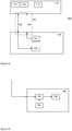
Figure 1a is a block diagram illustrating an electronic system for generating a cryptographic key, -
Figure 1b is a block diagram illustrating a key derivation unit for use in system offigure 1a , -
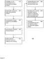
Figure 2 is a block diagram illustrating an electronic system for generating a cryptographic key. -
Figures 3a is a block diagram illustrating code word boundary preserving scrambling -
Figures 3b is a block diagram illustrating non-code word boundary preserving scrambling, -
Figure 4 is a flow chart illustrating a method for generating a cryptographic key. - It should be noted that items which have the same reference numbers in different Figures, have the same structural features and the same functions, or are the same signals. Where the function and/or structure of such an item has been explained, there is no necessity for repeated explanation thereof in the detailed description.
-
- 100
- an electronic system for generating a cryptographic key
- 110
- a memory used as a physically unclonable function
- 112, 114, 116
- memory locations
- 120
- a memory interface
- 122
- a data channel
- 124
- an address channel
- 130
- a PUF control block
- 140
- an address scrambler
- 150
- a key derivation unit
- 152
- a buffer
- 154
- a permutator
- 156
- error correction logic
- 200
- an electronic system for generating a cryptographic key
- 210
- a PUF control block
- 220
- a memory read-out unit
- 230
- a key derivation unit
- 240
- an encryption unit
- 250
- a decryption unit
- 255
- address generator
- 260
- a further memory
- 265
- a random key and seed derivation unit
- 270
- a buffer
- 280
- a combiner
- 285
- a helper data memory
- 290
- an error corrector
- 295
- a key derivation function unit
- 310
- memory content
- 312,314,316
- code-word sized memory chunks
- 320
- scrambled memory access
- 322,324,326
- code-word sized memory chunks
- 330
- scrambled memory access
- 510, 511, 512, 514
- an encryption phase
- 520
- a decryption phase
- While this invention is susceptible of embodiment in many different forms, there is shown in the drawings and will herein be described in detail one or more specific embodiments, with the understanding that the present disclosure is to be considered as exemplary of the principles of the invention and not intended to limit the invention to the specific embodiments shown and described.
-
Figure 1a and 1b illustrate as a schematic block diagram anelectronic system 100 for generating a cryptographic key. -
System 100 comprises amemory 110 used as a physically unclonable function (PUF). The memory is of a writable and volatile kind. Furthermore, the memory has the property that upon each powering-up of the memory the memory settles into a memory content which depends upon at least partially random physical characteristics of the memory. The physical environmental fluctuations are typically caused by small process variations during manufacture. - Since the memory content into which the memory settles depends upon such physical characteristics, the memory content identifies the particular instantiation of the memory. That is, two
memories 110 of the same design would show a memory content upon start-up which is sufficiently different to identify the memory. For example,memory 110 may be based upon flip-flops; in particular,memory 110 may be an SRAM. -
Memory 110 comprises a sequence of memory locations of which the power-up content is used as a PUF. The memory locations are accessible, that is read or write accessible, through a corresponding sequence of memory addresses. Of the sequence of memory locations three are shown 112, 114 and 116. -
System 100 comprises aPUF control block 130.PUF control block 130 is configured to process the memory content into whichmemory 110 settles at start-up to produce a cryptographic key. In its raw state the memory content is not directly usable as a key. The memory content ofmemory 110 upon power-up depends not only on its physical characteristics; the memory content is also influenced by noise. Furthermore, there is an influence of physical fluctuations in its environment, such as temperature, and mechanical stress on the memory. Since the memory content is subject to noise it is not directly useable as a cryptographic key. Also the entropy in a single bit may be too low. PUF control block 130 addresses these by error correcting and optionally key derivation. Error correction and the like are performed bykey derivation function 150, which is comprised incontrol block 130. - The
PUF control block 130 is connected tomemory 110 through amemory interface 120.Memory interface 120 comprises adata channel 122, e.g. data lines, and anaddress channel 124, e.g., address lines.Memory interface 120 may also comprise control lines and the like. - The use of memory interfaces has the drawback that it is a potential side-channel. The hamming weight of a word that is communicated over
data channel 122 may be determined by observing the power consumption ofsystem 100, while the word is transferred overdata channel 122. For example, if data channel 122 is 8 bit wide, each word could leaks on the order of 1-2 bits of information. Such leakage comprises the security of the entire system. -
Control block 130 comprises anaddress scrambler 140 for retrieving the memory content over the memory interface in a scrambled order. Preferably,address scrambler 140 implements a (pseudo)random permutation. For example,address scrambler 140 generates the sequence of memory addresses in the scrambled order. A convenient way to implementaddress scrambler 140 is by encrypting the sequence of memory addresses by a suitable sized encryption function. Conveniently, the size ofmemory 110 is chosen to be a power of 2, so that it may be one-to-one addressed by an integer number of bits. In that case, a block cipher may be used having a block width equal to the integer number of bits. Such block ciphers may be constructed using a Feistel cipher. The Feistel cipher may be unbalanced, for example, a so called Thorp shuffle may be used. More in general amemory 110 having any addressing scheme or any size may be accommodated using so-called format-preserving encryption. Format-preserving encryption bijectively maps the sequence of addresses onto itself. - When encryption is used,
address scrambler 140 may generate the sequence of addresses in any order, say linearly, and encrypt the sequence. Alternative ways to produce the sequence of addresses in a scrambled order may be used. For example,address scrambler 140 may comprise a feedback shift register, e.g., a linear feedback shift register configured to produce the sequence of memory addresses in a scrambled order. - The memory content in which
memory 110 settled is retrieved in the scrambled order. - In the system of
figure 1a, 1b , thekey derivation unit 150 receives the memory content in the scrambled order.Figure 1b shows one particular way to process the memory content. -
Key derivation function 150 comprises abuffer 152, apermutator 154 anderror correction logic 156. - Buffer 152 buffers the memory content received from
memory 110, e.g., from a memory read-out unit (not separately shown infigure 1a ).Permutator 154 performs the inverse permutation applied byaddress scramble 140.Permutator 154 may produce inbuffer 152 the memory content in the same order as it was produced inmemory 110. But,permutator 154 may produce inbuffer 152 the memory content in any pre-determined order, by performing a function composition of the inverse of the scrambling permutation with a permutation representing the pre-determined order.Permutator 154 may be connected, or even integrated with,scrambler 140, to obtain the correct descrambling operation. The result of the inverse permutation is passed on toerror correction logic 156.Error correction logic 156 corrects the noise by combining with helper data, and optionally, applies a key derivation function (KDF) to the result, e.g., the result could be hashed with a cryptographic hash function. Correction of noise in the memory content of a memory used as a PUF is known per se. One may include buffer 152 andpermutator 154 with the memory read-out unit instead of with the key derivation function. - As memory content only travels over the memory interface in scrambled form, it still reveals a hamming weight, however considerably less information is leaked since it is no longer known to which word the hamming weight corresponds.
- Although this a significant advantage, there are some drawbacks to the system of
figures 1a, 1b . First of all it requires a descrambling operation, performed bypermutator 154. This is a relatively costly operation especially if it is to be done in place. - If the
error correction logic 156 uses a single code word, then buffer 152 would be twice the size ofmemory 110 in order to use not-in place descrambling. This is relatively costly. However, preferably, the error correction uses multiple code words since smaller code word correction is more resource efficient. In that case the scrambling operation may be configured to respect code word boundaries, but there are other options, e.g. use a larger buffer or use other solution described herein.Figure 3a illustrates a scrambling operation. -
Memory content 310 is partitioned into code-word sized memory chunks.Figure 3a shows three such chunks 312,314,316. Each of the chunks may be error corrected independently of the other chunks. At 320 the same part of memory is depicted but with scrambled memory access. The arrows indicate the scrambled address corresponding to an original address. Note that this mapping respects code word boundaries. That is, the sequence of memory addresses comprises multiple code sequences of sequential memory addresses,address scrambler 140 generates a sequence of address such that each one multiple code sequences are generated together without being interleaved by addresses of a different sequence. Although such an address scrambling prevents less side channel leakage, it is still a marked improvement.Figure 3b shows a scrambledmemory access 330 which does not respect code word boundaries. Such a scrambling function prevents more leakage, but is harder (though not impossible) to accommodate by the key derivation function ofFigure 1 . The system described below with respect toFigure 2 is able to handle the scrambled memory access, such as scrambledmemory access 330, which does not necessarily respect code word boundaries using a two pass system. - Instead of using
permutator 154 it is also possible to take the scrambling into account during combination with helper data. In that casekey derivation unit 150 may comprise a combiner that reads frombuffer 152, and from a helper data-memory (neither shown infigure 1b ). This approach also has disadvantages: helper-data memory is usually a non-volatile memory, which is usually read out in blocks, so that random access in helper-data memory often carries a high performance penalty. -
Figure 2 illustrates an improvedelectronic system 200 for generating a cryptographic key.Figure 4 illustrates in a flow chart a method for generating a cryptographic key that may be performed usingsystem 200, although variations are possible. - Like
system 100,system 200 comprises amemory 110 used as a PUF connected through amemory interface 120 to aPUF control block 210. PUF control block comprises a memory read-outunit 220 andkey derivation unit 230. - Memory read-out
unit 220 is configured to securely read outmemory 110 in a pre-determined order. The pre-determined order is determined by what is convenient for the subsequent key derivation. Typically, the pre-determined order is the natural linear order, but any order is possible. For example, for increased obfuscation, a random but fixed pre-determined order may be selected, and helper data may be computed for the memory content permuted according to that random but fixed pre-determined order. From here on we will assume the pre-determined order is linear, but it is noted that this may be varied. The memory content is obtained by powering-up of memory 110 (step 410) and allowing the memory to settle into a memory content (step 420). The settling time depends on the memory, and may be determined experimentally if needed. Since settling time is typically much shorter than the booting functions that are typically performed on electronic computing devices, it is usually not needed to introduce a delay element which delays read-out of the memory for software implementations of the memory read out unit. -
Key derivation unit 230 receives the memory content into whichmemory 110 settled in the pre-determined order from memory read-outunit 220. In an embodiment one may use a known key derivation unit configured to perform usual PUF processing (error correction and typically a key derivation function). If a known key derivation unit is used, then from the perspective ofkey derivation unit 230 it receives memory content data as usual. This part of the system will thus only be given a cursory description. - Key derivation unit may comprise a
buffer 270.Buffer 270 is large enough to hold a single code word. Key derivation function may comprise acombiner 280 for combining the content of the buffer with helper data stored in ahelper data memory 285. We will assume that the combining function is the typical bit-wise XOR operation, although any invertible binary operation may be used, e.g., addition modulo the number of different word values, e.g., modulo 256 for a byte. The helper data may have been obtained by XOR-ing a previously obtained copy of the memory content with a code word of an error correcting code. The code word is secret, and may have been chosen at random from the error correcting code or selected according to some key management scheme. Duringoperation combiner 280 XORs the helper data with the memory content obtained inbuffer 270 to obtain a correctable bit string that lies in a neighborhood of the secret code word. Anerror corrector 290 applies an error correcting code algorithm corresponding to the error correcting code to obtain the secret code word again. If needed, a key derivation function unit applies a key derivation function (KDF), for example, a cryptographic hash function. The cryptographic function may be used for any cryptographic purpose, e.g., authentication, encryption, etc. - Interestingly, the error correction may use a two-pass system for error correction as well. The memory may be portioned into smaller words, which are individually corrected to code words, e.g., from a Hadamard code. The corrected smaller code words are combined into larger words which are to be corrected with a larger block size error correcting code, say a BCH code. The combining into larger words preferably interleaves the smaller code words. The key derivation function may write the corrected smaller code words back to the memory, in encrypted form. The key derivation function may perform random access on the memory, using the decryption unit, e.g., to perform the interleaving. In this
way memory 110 may be used as working memory for more complicated error correction schemes, while still reducing side-channel leakage; aftermemory 110 has been encrypted it supports random access read/write access through the encryption and decryption unit. - Key derivation unit may use countermeasures to reduce its side channel leakage if needed. For example, the device and method described in
WO/2010/100015 may be used. - The memory read-out unit comprises an
address scrambler 140 to retrieve the memory content over the memory interface in a scrambled order, and anencryption unit 240.Encryption unit 240 receives the data retrieved byscrambler 140 and encrypts it. The encrypted data, i.e., the encrypted memory content is written to a memory. Although any memory could be used, preferably the encrypted memory content is written back tomemory 110. To reduce the amount of needed memory, the memory content may be written back in the same scrambled order, thereby overwriting the memory content with the encrypted memory content; each encrypted memory word is written back to the same scrambled address from which it was read. Togetherencryption unit 240 and scramblingunit 140 may have the effect of encrypting the memory in place, but in a scrambled order. -
Encryption unit 240 may be a block cipher. For example,encryption unit 240 may operate in electronic code book mode (ECB). For example,encryption unit 240 may operate in counter mode (CTR), e.g., encrypting the address in ECB mode and XOR-ing the result to the memory content. Since the block size is often quite small, say, 8, 16, or 32 bits, the latter is preferred since it obscures the relation between words in the memory content which happen to have equal values. - The encryption unit needs a key. The address scrambler needs either a seed, or in case address encryption is used also a key. The key may be fixed, but more preferably it is produced at start-up of memory read-out
unit 220. The key/seed may be produced randomly, either true or pseudo random. For example, memory read-outunit 220 may comprise a true random number generator (not shown). - However, it is observed that randomness is typically only needed during power-up of memory read-out
unit 220. This allows another solution which is shown infigure 2 . Memory read-outunit 220 comprises a further memory 260 (preferably internal to thePUF control block 210 and different from memory 110). Alsofurther memory 260 is volatile. Upon each powering-up of the further memory the second memory settles into a noisy memory content. Note that the content of the further memory will also depend on its physical characteristics, but for this purpose the noise in the memory content is exploited. Random key andseed derivation unit 265 derives a key and/or seed from the memory content ofmemory 265, for example, by applying a hash function to the content ofmemory 260. Should a new key/seed be needed, for example to re-read the contents ofmemory 110 later, without a new powering-up then a new key and new seed may be obtained by applying a one-way function to the old seed. - Memory read-out
unit 220 further comprises adecryption unit 250 and anaddress generator 255.Address generator 255 may be combined withdecryption unit 250.Address generator 255 is configured to produce the sequence of memory address in the pre-determined order.Decryption unit 250 then decrypts the received encrypted memory content. - Thus a secure read-out is obtained in two passes. In a first pass the memory in encrypted. This pass suffers less from side-channel leakage, since access to the memory is in a scrambled order. In the second pass the memory is read-out in any desired order, such as a pre-determined order. The second pass more secure since all data that passes over the memory interface is encrypted. An advantage of
system 200 oversystem 100 is that any scrambling function may be used even without respecting code word boundaries, while key derivation may still work on smaller sized code words. -
System System system -
Figure 4 illustrates in a flow chart a method for generating a cryptographic key. The method offigure 4 may be performed usingsystem 200, although variations are possible. - Operation of
system 200 may be done as follows. First the system is powered-up. (Step 410) During the powering up,memory 110 is powered-up and allowed to settle in its memory content (step 420). The memory content ofmemory 110 is representative for this particular memory although it may be noisy. The read-out of this memory content is done in two passes: In the first pass, the memory content is retrieved (step 430) in a scrambled order, say byscrambler 140,step 430 and received for encryption, say byencryption unit 240. The memory content is encrypted (step 440) and written back (step 450). In a second pass, the encrypted memory content is retrieved, say by anaddress generator 255 in a pre-determined order, say the linear sequential order, and received by a decryption unit 250 (step 460). The encrypted memory content is decrypted to obtain the memory content in whichmemory 110 settled in the pre-determined order (step 470). - At this point the memory content has securely passed from
memory 110 overmemory interface 120 with no or minimal side channel leakage. PUF processing may proceed, by combining the memory content with helper data to obtain one or more correctable bit-strings. A correctable bit-string lies in a correctable neighborhood of an error correcting code. The one or more correctable bit-strings may be error-corrected to establish a code word of an error correcting code using an error correcting algorithm. A key may be derived from the established code word by applying a KDF. - In
steps steps steps - Many different ways of executing
method 400 are possible, as will be apparent to a person skilled in the art. For example, the order of the steps can be varied or some steps may be executed in parallel. Moreover, in between steps other method steps may be inserted. The inserted steps may represent refinements of the method such as described herein, or may be unrelated to the method. For example, steps 470 and 480 may be executed, at least partially, in parallel. Moreover, a given step may not have finished completely before a next step is started. - A method according to the invention may be executed using software, which comprises instructions for causing a processor system to perform
method 400. Software may only include those steps taken by a particular sub-entity of the system. The software may be stored in a suitable storage medium, such as a hard disk, a floppy, a memory etc. The software may be sent as a signal along a wire, or wireless, or using a data network, e.g., the Internet. The software may be made available for download and/or for remote usage on a server. - It will be appreciated that the invention also extends to computer programs, particularly computer programs on or in a carrier, adapted for putting the invention into practice. The program may be in the form of source code, object code, a code intermediate source and object code such as partially compiled form, or in any other form suitable for use in the implementation of the method according to the invention. An embodiment relating to a computer program product comprises computer executable instructions corresponding to each of the processing steps of at least one of the methods set forth. These instructions may be subdivided into subroutines and/or be stored in one or more files that may be linked statically or dynamically. Another embodiment relating to a computer program product comprises computer executable instructions corresponding to each of the means of at least one of the systems and/or products set forth.
-
Figure 5a-5d illustrates different possibilities for scrambling and encrypting the memory. For simplicity only 8 memory location of the memory are shown, the memory content extends at least over these 8 memory locations. In practice a much larger memory may be used. In the figures, memory locations are indicated with a number of 1 to 8. A memory location may be, e.g., a word, such as an 8 bit word, or a 16 bit word, etc; read access to a memory access is indicated with an 'R', and write access by a 'W'; an obfuscating access is indicated with an 'A'. The obfuscating access may be a read, a write, or a combination of a read and write to the same memory location; Time increases from left to right. - In
figure 5a , two phases are shown anencryption phase 510 andsubsequent decryption phase 520. During the encryption phase the memory read-out unit iteratively: reads from a memory location, i.e., from a memory address, encrypts the content read from the memory address, and writes back to the same memory address. The memory addresses are scrambled by the address scrambler. At the end of theencryption phase 510 the entire memory content has been encrypted, even though the memory has been read in a scrambled order. The particular scrambled order shown infigure 5a is exemplary. - During the decryption phase the decryption unit received the encrypted memory content in a further order. The further order used in the
figure 5a is the natural sequential order. Typically, the scrambled order is different when subsequent power-ups of the same device are compared but the further order is the same. To have best performance during key derivation or error correction etc, it is preferred to start thedecryption phase 520 after the encryption phase ended. This is not strictly necessary, for example, after an encrypted write back to the first memory location of the further order has taken place, the decryption phase may commence with reading that location, after the next memory location of the further order has taken place, the decryption phase can continue to one further decryption. This increase in complexity will only be worthwhile when obfuscation needs to be maximal even at the expense of additional complexity. Infigures 5b-5d we will assume that this is not done, the decryption phases are thus the same as infigure 5a and not shown separately. - The embodiment of
figure 5a in which the encryption phases comprises repeated cycles of read and encrypted write back to a sequence of scrambled memory addresses may be varied in multiple different ways. Such variations help in preventing advanced attacks. - The read and write accesses during encryption phase need not be strictly alternating. For example, the encryption phase may read multiple memory contents, encrypt them and write back multiple encrypted memory content. The order in which the write back occurs may be the same or may not be the same as the order in which they were read. The encrypted order may be linear or re-scrambled.
Figure 5b shows anencryption phase 511, wherein the read and write operations are done in multiple batches of, in this case, each 4 read and 4 writes. The batch uses linear write back, the second batch uses scrambled write back. Batches improve over the 5a case by making it harder to correlate the read value and its encryption, per address. - Recently photo-emission attacks have been demonstrated that target SRAM directly by recording photon activity from the back side of the SRAM structure during access. Photon emission attacks are based on the fact that electronic devices tend to emit photons with a certain probability when in operation. The photon generation rate is proportional to the supply voltage and the transistor switching frequency. In particular the reading of SRAM values also causes photons to be emitted. When aiming a CCD at the backside of an IC it is possible to collect information on the memory content by recording the read operations. Photonic Emission Analysis may assist other cryptanalytic methods and/or side channels.
- Potentially, photo-emission attacks could be used to attack SRAM PUFs as well, e.g., to record the very first read of each PUF SRAM address. If a full read-out of the power-up memory content of the SRAM could be obtained, this would lead to a serious security problem. For example, if the recording of the photonic emission could be programmed so that it exactly captures all first reads, and nothing more from the SRAM, and repeating the measurement many times, a reliable image of the SRAM startup values could be assembled.
- Scrambling of the reading order on its own would not be sufficient to counter a photonic attack: the randomization does not change the picture because the picture is simply the sum total of all initial read actions regardless of their order. Fortunately, in a read-out as in
Figure 5a and, to a lesser extent, infigure 5b , the read outs that are correlated to the memory content in which the memory settled into at powering-up are interspersed with write backs which are not so correlated. This will make it much harder to use photonic information. To attack this set-up an attacker may use a shutter mechanism to single out (first) read accesses. The shutter is configured in an open position during reads and in a close position during writes. In this way only the photon emission during unencrypted reads are recorded. In an embodiment, the memory read-out unit is configured to select a batch size at least partially at random, and is configured to perform a batch size number of read operations through the address scrambler followed by a batch size number of encrypted write-back operations by the encryption unit. For example, the batch size may be selected at start-up, for example, the batch size may be selected repeatedly, e.g., after each batch size read. At least partially random may be achieved by making the batch size dependent upon part of the PUF. For example, the batch size may be randomly selected from 1, 2, 3, 4 bytes. - However, it is desirable to reduce the signal that is correlated to the power-up content even further.
- This can be achieved by introducing additional randomized accesses, e.g. writes and/or reads to each memory location. The writes will overwrite the initial value, and all subsequent reads will emit confusing information. To make this countermeasure more effective, the additional writes and reads per address need to be ordered randomly with respect to similar writes and reads to other addresses.
- Doing additional reads and writes to the SRAM in a randomized order, generates more photonic activity that is hard to separate from the initial PUF data reads. The data used for the additional writes can be random data, a fixed pattern or even a device-specific pattern, where part of the PUF is used to derive a device-specific pattern. Also combinations of these three can be used. Randomizing this order can be based on a random seed that is itself based on a PUF startup value. The randomization makes it hard to single out first-time read accesses for all memory locations.
- The scrambled read-out and encrypted write back preparation step can be enhanced to significantly hamper this attack. This is achieved by, in addition to scrambling the reading order, merging the read-out and encrypted write-back stages.
- By adding additional reads of the encrypted data, e.g., reading several times from each address, and mixing first-time reads with subsequent, encrypted data reads in a randomized -e.g. based on PUF-harvested random seed- way, it is not possible for an attacker to predict the exact schedule of reads and writes as this schedule will be different for each power-up. As a result it is very hard to create a reliable picture of the SRAM startup values.
- For example, the
encryption phase 512 offigure 5c shows the same scrambled order as in figure 510, however additional obfuscating accesses were added. The obfuscating accesses are done by obfuscation unit, e.g. comprised in read-outunit 210. For example, the obfuscating unit may have the opportunity to insert an obfuscating accesses after each read and/or write access of the rest ofunit 210. InFigure 5c the obfuscating accesses are done only to memory locations to which an encrypted write-back already occurred. - Different types of access are advantageous. An access could be an additional read. This is simpler to implement, as it avoids the question what value needs to be written. An access could be a read/write cycle. Write accesses are more likely to cause photonic emission thus causing additional obfuscation. An access could be a read/write/write cycle; in the first write a random value or a fixed value, say all 1, or the inverse of the read value is written, then in the second write the value read is written back. This will increase switches in the memory location and further increase photonic emission. Performing an obfuscating access may thus comprise selecting a memory location, i.e. address, preferably one to which the encrypted write already occurred, and performing the access to the selected memory address.
- The access could also be write access, in the latter case care must be taken that the correct value is written. A particular good tradeoff between effect and ease of implementation is shown in
figure 5d . Infigure 5d the encryption phase consists of multiple read/write-back cycles. The write is repeated to increase photonic effect of the encrypted (thus uncorrelated) write-back. Also in this scenario, the first write could be random, inverse, fixed. Unfortunately,figure 5d exhibits a regular pattern RiWiWi which makes vulnerable to single out Ri using a shutter; in an embodiment the read/write pattern is enhanced with random interleaving. For example, the number of write operations may be partially random, for example, the a batch size number may be selected, as indicated above, however the batch size number is only used to control the number of repetitions of the write-back. Other random interleaves may also be used. - Having two write backs in which the first is the inverse of the encrypted write-back increases photonic emission which reduces the effect of a possible photonic emission in the first read.
- In an embodiment, the obfuscation unit is configured to perform an obfuscating access to a memory location in the memory, the obfuscating access being performed after the encryption unit wrote encrypted memory content back to the memory location. There are various ways in which the obfuscation unit may keep track of which memory locations are safe to access. In a further embodiment, the obfuscating access is before the decryption unit received encrypted memory content from the memory location.
- In another embodiment, the obfuscation unit performs read accesses from a random memory location. At fixed points during the encryption phase, say after each scrambled read and after each write-back, the obfuscation unit has the opportunity to insert an obfuscating access, preferably read access, to a random memory location. The obfuscation unit comprises a probability value which indicates the probability that the obfuscation unit will insert the obfuscating access. At the start of the encryption phase the probability value is at a lower value and during at least the encryption phase the probability value increases so that at the end of the encryption phase the probability value is at a high value. For example, the probability value may increase linearly after each opportunity, from a fixed start value to a fixed end value.
- At the beginning of the encryption phase only a small part of the memory has been encrypted, additional reads run the risk of improving the signal for the attacker, however in this stage the probability of a read is low, at the end a large part of the memory is encrypted, to the probability of read of an encrypted value is high. The advantage of this scheme is that no book-keeping is needed to keep track of which memory locations are safe for reading from, i.e., have an encrypted value. In an embodiment, the probability value increases linearly form 0.1 to 0.9 from start to end of the encryption phase. An embodiment of the electronic memory read-out unit for securely reading out a memory in a further order comprises any one of the obfuscation units described herein
- It should be noted that the above-mentioned embodiments illustrate rather than limit the invention, and that those skilled in the art will be able to design many alternative embodiments.
- In the claims, any reference signs placed between parentheses shall not be construed as limiting the claim. Use of the verb "comprise" and its conjugations does not exclude the presence of elements or steps other than those stated in a claim. The article "a" or "an" preceding an element does not exclude the presence of a plurality of such elements. The invention may be implemented by means of hardware comprising several distinct elements, and by means of a suitably programmed computer. In the device claim enumerating several means, several of these means may be embodied by one and the same item of hardware. The mere fact that certain measures are recited in mutually different dependent claims does not indicate that a combination of these measures cannot be used to advantage.
Claims (18)
- An electronic system (100; 200) for generating a cryptographic key, the system comprising- a memory (110) used as a physically unclonable function, the memory being writable, volatile and configured such that upon each powering-up of the memory the memory settles into a memory content which depends upon at least partially random physical characteristics of the memory, the memory being accessible through a memory interface (120), and- a key derivation unit (150; 230) configured to derive the cryptographic key from the memory content into which the memory settled,
wherein the electronic system for generating a cryptographic key further comprises,- a memory read-out unit (220) connected to the memory through the memory interface and to the key derivation unit, the memory read-out unit comprising- an address scrambler (140) for retrieving the memory content over the memory interface in a scrambled order, and an address generator (255) for retrieving the memory content in a pre-determined further order, wherein the scrambled order is derived from a seed at least partially randomly generated after each power-up of the read-out unit,- an encryption unit (240) for encrypting the memory with a temporary key, the encryption unit being configured to receive from the memory interface the memory content retrieved by the address scrambler in the scrambled order, encrypt the received memory content and write back the encrypted memory content to the memory, and- a decryption unit (250) for decrypting the memory, configured to receive from the memory interface the encrypted memory content retrieved by the address generator (255) in the pre-determined further order, decrypt the received encrypted memory content to obtain the memory content in the pre-determined further order,wherein read-out of the memory for the key derivation unit is done in two passes, in a first pass the memory is encrypted, wherein access to the memory is in a scrambled order, and in a second pass the memory is read-out in the pre-determined order, wherein data that passes over the memory interface is encrypted. - An electronic system as in claim 1, comprising- a non-volatile helper-data memory (285), the helper-data memory storing helper data constructed for the memory used as a physically unclonable function,- a combiner (280) for establishing a correctable bit-string, the correctable bit-string lying in a correctable neighborhood of an error correcting code, the combiner being configured to retrieve the helper data from the helper-data memory and to combine the retrieved helper data with the memory content into which the memory settled in the pre-determined further order obtained from the memory read-out unit,- an error-corrector (290) configured to establish a code word of an error correcting code from the correctable bit-string using an error correcting algorithm.
- An electronic system as in any one of the preceding claims, wherein the encryption unit is configured to write back the encrypted memory content to the memory in the scrambled order thereby overwriting the memory content with the encrypted memory content
- An electronic system as in any one of the preceding claims, wherein the pre-determined further order is the linear order.
- An electronic system as in claim 1, wherein the read-out unit comprises a cryptographic one-way function configured to be applied to the seed to obtain a new seed, the address scrambler being configured to derive a new scrambled order from the new seed for re-fetching the memory content over the memory interface in the new scrambled order.
- An electronic system in any one of Claims 1 and 4, wherein the read-out unit comprises a further volatile memory configured such that upon each powering-up of the further memory the second memory settles into a noisy memory content, the seed being derived from the memory content into which the second memory settled.
- An electronic system as in any one of the preceding claims, comprising an obfuscation unit, the obfuscation unit being configured to perform a number of additional obfuscating accesses to the memory, the obfuscating access being configured to reduce the correlation between photo-emissions from the memory and memory content in which the memory settled into at powering-up.
- An electronic system as in Claim 7, the obfuscation unit is configured to perform an obfuscating access to a memory location in the memory, the obfuscating access being performed after the encryption unit wrote encrypted memory content back to the memory location.
- An electronic system as in any one of the preceding claims, wherein the memory read-out unit is configured to select a batch size at least partially at random, and is configured to perform a batch size number of read operations through the address scrambler followed by a batch size number of encrypted write-back operations by the encryption unit.
- An electronic system as in claim 2, wherein- the memory content is partitioned into code-word sized memory chunks, the error-corrector (290) being configured to establish multiple code words from the correctable bit-string, each of the chunks being error corrected independently of the other chunks,- the address scrambler (140) is configured to generate a sequence of memory addresses of memory (110) in a scrambled order, the sequence of memory addresses comprises multiple code sequences of sequential memory addresses corresponding to the memory chunks, the address scrambler (140) generating the sequence of address such that each one of the multiple code sequences is generated together without being interleaved by addresses of a different one of the multiple code sequence.
- An electronic system as in any one of the preceding claims, wherein the memory used as a physically unclonable function is an SRAM memory.
- An electronic system as in any one of the preceding claims, wherein the memory used as a physically unclonable function is volatile FPGA memory.
- An integrated circuit comprising the electronic system for generating a cryptographic key according to any one of the preceding claims.
- An integrated circuit according to claim 13, wherein the integrated circuit is any one of a smart card, an ASSP, DSP, Application processor, SIM and NFC chip.
- An electronic memory read-out unit for securely reading out a memory in a pre-determined further order, the memory being writable, the electronic memory read-out unit being connectable to the memory through a memory interface, the memory read-out unit comprising- an address scrambler configured to retrieve the memory content over the memory interface in a scrambled order, and an address generator (255) for retrieving the memory content in a pre-determined further order, wherein the scrambled order is derived from a seed at least partially randomly generated after each power-up of the read-out unit,- an encryption unit for encrypting the memory with a temporary key, the encryption unit being configured to receive from the memory interface the memory content retrieved by the address scrambler in the scrambled order, encrypt the received memory content and write back the encrypted memory content, and- a decryption unit for decrypting the memory, configured to receive from the memory interface the encrypted memory content retrieved by the address generator (255) in the pre-determined further order, decrypt the received encrypted memory content to obtain the memory content in the pre-determined further order,wherein the secure read-out of the memory is done in two passes, in a first pass the memory is encrypted, wherein access to the memory is in a scrambled order, and in a second pass the memory is read-out in the pre-determined order, wherein data that passes over the memory interface is encrypted.
- A method for generating a cryptographic key (400), the method comprising- powering-up (410) of a memory used as a physically unclonable function, the memory being writable and volatile,- allowing (420) the memory to settle into a memory content which depends upon at least partially random physical characteristics of the memory,- retrieve (430) the memory content over a memory interface in a scrambled order, and retrieve the memory content in a pre-determined further order, wherein the scrambled order is derived from a seed at least partially randomly generated after each power-up of a read-out unit,- encrypting the memory by- receiving (430) from the memory interface the memory content in the scrambled order,- encrypting (440) the received memory content, and- writing back (450) the encrypted memory content to the memory, and- decrypting the memory by,- receiving (460) from the memory interface the encrypted memory content in the pre-determined further order, and- decrypting (470) the received encrypted memory content to obtain the memory content in the pre-determined further order- deriving (480) a cryptographic key from the memory content into which the memory settledwherein read-out of the memory for the key derivation unit is done in two passes, in a first pass the memory is encrypted, wherein access to the memory is in a scrambled order, and in a second pass the memory is read-out in the pre-determined order, wherein data that passes over the memory interface is encrypted.
- A computer program comprising computer program code means adapted to perform all the steps of claim 16 when the computer program is run on a computer.
- A computer program as claimed in claim 17 embodied on a computer readable medium.
Priority Applications (1)
| Application Number | Priority Date | Filing Date | Title |
|---|---|---|---|
| EP13759256.4A EP2904732B1 (en) | 2012-10-04 | 2013-09-10 | System for generating a cryptographic key from a memory used as a physically unclonable function |
Applications Claiming Priority (4)
| Application Number | Priority Date | Filing Date | Title |
|---|---|---|---|
| EP12187213 | 2012-10-04 | ||
| EP12194713 | 2012-11-29 | ||
| EP13759256.4A EP2904732B1 (en) | 2012-10-04 | 2013-09-10 | System for generating a cryptographic key from a memory used as a physically unclonable function |
| PCT/EP2013/068746 WO2014053286A1 (en) | 2012-10-04 | 2013-09-10 | System for generating a cryptographic key from a memory used as a physically unclonable function |
Publications (2)
| Publication Number | Publication Date |
|---|---|
| EP2904732A1 EP2904732A1 (en) | 2015-08-12 |
| EP2904732B1 true EP2904732B1 (en) | 2018-11-28 |
Family
ID=49118557
Family Applications (1)
| Application Number | Title | Priority Date | Filing Date |
|---|---|---|---|
| EP13759256.4A Active EP2904732B1 (en) | 2012-10-04 | 2013-09-10 | System for generating a cryptographic key from a memory used as a physically unclonable function |
Country Status (6)
| Country | Link |
|---|---|
| US (1) | US9430406B2 (en) |
| EP (1) | EP2904732B1 (en) |
| JP (1) | JP6267207B2 (en) |
| KR (1) | KR102201062B1 (en) |
| CN (1) | CN104704768B (en) |
| WO (1) | WO2014053286A1 (en) |
Families Citing this family (81)
| Publication number | Priority date | Publication date | Assignee | Title |
|---|---|---|---|---|
| DE102014208210A1 (en) * | 2014-04-30 | 2015-11-19 | Siemens Aktiengesellschaft | Derive a device-specific value |
| US9672342B2 (en) | 2014-05-05 | 2017-06-06 | Analog Devices, Inc. | System and device binding metadata with hardware intrinsic properties |
| US9946858B2 (en) | 2014-05-05 | 2018-04-17 | Analog Devices, Inc. | Authentication system and device including physical unclonable function and threshold cryptography |
| US10432409B2 (en) | 2014-05-05 | 2019-10-01 | Analog Devices, Inc. | Authentication system and device including physical unclonable function and threshold cryptography |
| IL234956A (en) * | 2014-10-02 | 2017-10-31 | Kaluzhny Uri | Bus protection with improved key entropy |
| US9640247B2 (en) | 2015-01-14 | 2017-05-02 | Qualcomm Incorporated | Methods and apparatuses for generating random numbers based on bit cell settling time |
| EP3046095B1 (en) * | 2015-01-15 | 2021-10-20 | Siemens Aktiengesellschaft | A method of protecting diverse applications stored on an integrated circuit using PUFs |
| EP3046096B1 (en) | 2015-01-15 | 2022-03-30 | Siemens Aktiengesellschaft | A protection method of writting encrypted data to a memory device and reading decrypted data from the memory device using the power up of a PUF |
| US9425803B1 (en) * | 2015-05-07 | 2016-08-23 | The United States Of America As Represented By The Secretary Of The Navy | Apparatuses and methods for implementing various physically unclonable function (PUF) and random number generator capabilities |
| US9875378B2 (en) | 2015-06-12 | 2018-01-23 | QUALCOMOM Incorporated | Physically unclonable function assisted memory encryption device techniques |
| US10318431B2 (en) | 2015-09-17 | 2019-06-11 | Hewlett Packard Enterprise Development Lp | Obscuration of a cache signal |
| US20170126414A1 (en) * | 2015-10-28 | 2017-05-04 | Texas Instruments Incorporated | Database-less authentication with physically unclonable functions |
| EP3378054B1 (en) * | 2015-11-20 | 2021-03-17 | Intrinsic ID B.V. | Puf identifier assignment and testing method and device |
| DE102016201665A1 (en) * | 2016-02-03 | 2017-08-03 | Siemens Aktiengesellschaft | Encrypt the memory contents of a memory in an embedded system |
| US10572651B2 (en) | 2016-02-16 | 2020-02-25 | Samsung Electronics Co., Ltd. | Key generating method and apparatus using characteristic of memory |
| US10097348B2 (en) * | 2016-03-24 | 2018-10-09 | Samsung Electronics Co., Ltd. | Device bound encrypted data |
| US11843597B2 (en) * | 2016-05-18 | 2023-12-12 | Vercrio, Inc. | Automated scalable identity-proofing and authentication process |
| US10341122B2 (en) * | 2016-07-15 | 2019-07-02 | Hiroshi Watanabe | Electronic appliance and network of the same |
| US10715340B2 (en) | 2016-08-04 | 2020-07-14 | Macronix International Co., Ltd. | Non-volatile memory with security key storage |
| US10911229B2 (en) | 2016-08-04 | 2021-02-02 | Macronix International Co., Ltd. | Unchangeable physical unclonable function in non-volatile memory |
| US11258599B2 (en) | 2016-08-04 | 2022-02-22 | Macronix International Co., Ltd. | Stable physically unclonable function |
| US10855477B2 (en) | 2016-08-04 | 2020-12-01 | Macronix International Co., Ltd. | Non-volatile memory with physical unclonable function and random number generator |
| US10680809B2 (en) | 2016-08-04 | 2020-06-09 | Macronix International Co., Ltd. | Physical unclonable function for security key |
| CN106301786B (en) * | 2016-08-10 | 2019-04-02 | 南京航空航天大学 | A kind of physics unclonable function response error correction circuit based on SRAM type memory |
| US10318748B2 (en) * | 2016-09-30 | 2019-06-11 | Intel Corporation | Techniques to protect fuses against non-destructive attacks |
| US10387660B1 (en) * | 2016-10-17 | 2019-08-20 | National Technology & Engineering Solutions Of Sandia, Llc | Computational optical physical unclonable function |
| US10394492B2 (en) * | 2016-10-26 | 2019-08-27 | Lenovo Enterprise Solutions (Singapore) Pte. Ltd. | Securing a media storage device using write restriction mechanisms |
| US9811689B1 (en) | 2016-12-27 | 2017-11-07 | Macronix International Co., Ltd. | Chip ID generation using physical unclonable function |
| US10082975B1 (en) | 2017-03-02 | 2018-09-25 | Micron Technology, Inc. | Obfuscation-enhanced memory encryption |
| JP6882666B2 (en) * | 2017-03-07 | 2021-06-02 | 富士通株式会社 | Key generator and key generator |
| CN106933752B (en) * | 2017-03-09 | 2019-10-08 | 西安电子科技大学 | A kind of encryption device and method of SRAM type FPGA |
| WO2018183572A1 (en) * | 2017-03-29 | 2018-10-04 | Board Of Regents, The University Of Texas System | Reducing amount of helper data in silicon physical unclonable functions via lossy compression without production-time error characterization |
| KR101974465B1 (en) * | 2017-05-25 | 2019-08-23 | 한밭대학교 산학협력단 | Noise coupled physical unclonable functions system |
| US10425235B2 (en) | 2017-06-02 | 2019-09-24 | Analog Devices, Inc. | Device and system with global tamper resistance |
| US10958452B2 (en) | 2017-06-06 | 2021-03-23 | Analog Devices, Inc. | System and device including reconfigurable physical unclonable functions and threshold cryptography |
| US11093588B2 (en) * | 2017-06-26 | 2021-08-17 | Micron Technology, Inc. | Memory system including data obfuscation |
| CN107196766B (en) * | 2017-07-20 | 2023-04-14 | 中国工程物理研究院电子工程研究所 | Miniaturized quantum authentication system |
| EP3435586B1 (en) * | 2017-07-25 | 2019-08-07 | Intrinsic ID B.V. | Method to reduce aging of a cache memory |
| US10949546B2 (en) | 2017-08-02 | 2021-03-16 | Samsung Electronics Co., Ltd. | Security devices, electronic devices and methods of operating electronic devices |
| JP6538908B2 (en) * | 2017-09-12 | 2019-07-03 | 力旺電子股▲ふん▼有限公司eMemory Technology Inc. | Security system using entropy bit |
| CN107908980B (en) * | 2017-10-10 | 2021-11-23 | 芯海科技(深圳)股份有限公司 | Method for realizing encryption protection of memory data |
| US11050574B2 (en) * | 2017-11-29 | 2021-06-29 | Taiwan Semiconductor Manufacturing Company, Ltd. | Authentication based on physically unclonable functions |
| CN108229215A (en) * | 2017-12-06 | 2018-06-29 | 杭州中天微系统有限公司 | A kind of scrambled storage device in address and method |
| CN108182371A (en) * | 2017-12-22 | 2018-06-19 | 杭州中天微系统有限公司 | The chip external memory address scrambling apparatus and method of a kind of system on chip |
| CN110018810B (en) * | 2018-01-10 | 2021-05-18 | 力旺电子股份有限公司 | Random code generator |
| JP6894012B2 (en) * | 2018-01-23 | 2021-06-23 | ヌヴォトンテクノロジージャパン株式会社 | Non-volatile memory device and its writing method |
| JP6752247B2 (en) * | 2018-03-09 | 2020-09-09 | 三菱重工業株式会社 | Information distribution device, distribution target device, information distribution system, information distribution method and program |
| US11265151B2 (en) | 2018-03-09 | 2022-03-01 | Arizona Board Of Regents On Behalf Of Northern Arizona University | Key exchange schemes with addressable elements |
| EP3562092A1 (en) * | 2018-04-26 | 2019-10-30 | Thales Dis Design Services Sas | Method for generating on-board a cryptographic key using a physically unclonable function |
| US10742406B2 (en) * | 2018-05-03 | 2020-08-11 | Micron Technology, Inc. | Key generation and secure storage in a noisy environment |
| US11063755B2 (en) * | 2018-05-07 | 2021-07-13 | Cryptography Research, Inc. | Generating a key at a device based on a memory of the device |
| EP3811220B1 (en) * | 2018-06-11 | 2023-08-09 | Cryptography Research, Inc. | Generating a target data based on a function associated with a physical variation of a device |
| US11113422B2 (en) | 2018-08-03 | 2021-09-07 | Micron Technology, Inc. | Data protection in computer processors |
| US11074198B2 (en) * | 2018-09-18 | 2021-07-27 | Micron Technology, Inc. | Key management in computer processors |
| US11303462B2 (en) | 2018-11-19 | 2022-04-12 | Arizona Board Of Regents On Behalf Of Northern Arizona University | Unequally powered cryptography using physical unclonable functions |
| KR102263877B1 (en) * | 2018-12-18 | 2021-06-14 | 시큐리티플랫폼 주식회사 | Unique encryption key generator for device and method thereof |
| CN109656840A (en) * | 2018-12-21 | 2019-04-19 | 成都海光集成电路设计有限公司 | A kind of device of data encrypting and deciphering, method, storage medium and data-storage system |
| US11233662B2 (en) * | 2018-12-26 | 2022-01-25 | Arizona Board Of Regents On Behalf Of Northern Arizona University | Keyless encrypting schemes using physical unclonable function devices |
| TWI734314B (en) | 2018-12-31 | 2021-07-21 | 美商美光科技公司 | Systems, methods and non-transitory computer-readable medium for providing a digital fingerprint to a host device |
| US11514174B2 (en) * | 2019-01-23 | 2022-11-29 | Micron Technology, Inc. | Memory devices with cryptographic components |
| US11218330B2 (en) | 2019-03-25 | 2022-01-04 | Micron Technology, Inc. | Generating an identity for a computing device using a physical unclonable function |
| US11323275B2 (en) | 2019-03-25 | 2022-05-03 | Micron Technology, Inc. | Verification of identity using a secret key |
| KR102169468B1 (en) | 2019-05-20 | 2020-10-23 | 충북대학교 산학협력단 | Challenge scrambler for physical unclonable function |
| CN114303341A (en) * | 2019-06-07 | 2022-04-08 | 俄亥俄州国家创新基金会 | System and method for using a hybrid Boolean network as a physically unclonable function |
| US11343108B2 (en) * | 2019-06-12 | 2022-05-24 | Arizona Board Of Regents On Behalf Of Northern Arizona University | Generation of composite private keys |
| US11483167B2 (en) * | 2019-06-20 | 2022-10-25 | Intel Corporation | Method and apparatus to provide memory based physically unclonable functions |
| US11194978B2 (en) * | 2019-07-12 | 2021-12-07 | Northrop Grumman Systems Corporation | Combined radio frequency identification (RFID)-based asset management and component authentication |
| US20210051010A1 (en) * | 2019-08-16 | 2021-02-18 | PUFsecurity Corporation | Memory Device Providing Data Security |
| EP4042301A4 (en) * | 2019-10-08 | 2023-10-25 | Cryptography Research, Inc. | Encrypted physically unclonable function circuit helper data |
| US11516028B2 (en) | 2019-12-24 | 2022-11-29 | CERA Licensing Limited | Temperature sensing physical unclonable function (PUF) authentication system |
| GB201919297D0 (en) | 2019-12-24 | 2020-02-05 | Aronson Bill | Temperature sensing physical unclonable function (puf) authenication system |
| KR20210129370A (en) | 2020-04-20 | 2021-10-28 | 삼성전자주식회사 | Memory modules and semiconductor memory devices |
| US20210409233A1 (en) * | 2020-06-26 | 2021-12-30 | Taiwan Semiconductor Manufacturing Company Ltd. | Puf method and structure |
| CN112104459B (en) * | 2020-09-10 | 2023-05-12 | 国网江苏省电力有限公司信息通信分公司 | Key generation method based on channel fingerprint and auxiliary data |
| US11380379B2 (en) | 2020-11-02 | 2022-07-05 | Macronix International Co., Ltd. | PUF applications in memories |
| US11604740B2 (en) * | 2020-12-01 | 2023-03-14 | Capital One Services, Llc | Obfuscating cryptographic material in memory |
| CN113037488B (en) * | 2021-04-19 | 2022-07-22 | 工业信息安全(四川)创新中心有限公司 | Format-preserving encryption method and decryption method based on cryptographic hash algorithm |
| US20230033630A1 (en) * | 2021-07-30 | 2023-02-02 | Micron Technology, Inc. | Embedded Hardware Security Module (HSM) |
| WO2023107287A1 (en) * | 2021-12-06 | 2023-06-15 | Cryptography Research, Inc. | Physically uncloneable function as secure storage |
| CN114912154B (en) * | 2022-06-06 | 2024-03-15 | 山东大学 | Encryption and calculation integrated implementation method based on nonvolatile memory |
| CN115216861B (en) * | 2022-07-22 | 2023-07-28 | 河南大学 | PUF device based on metal-dielectric-luminous coaxial multilayer composite nanofiber and method for generating secret key by using device |
Family Cites Families (9)
| Publication number | Priority date | Publication date | Assignee | Title |
|---|---|---|---|---|
| US7310706B1 (en) * | 2001-06-01 | 2007-12-18 | Mips Technologies, Inc. | Random cache line refill |
| JP2003018143A (en) * | 2001-06-28 | 2003-01-17 | Mitsubishi Electric Corp | Information processor |
| EP1891770B1 (en) | 2005-06-01 | 2011-10-05 | Priv Id B.V. | Template renewal in helper data systems |
| US8638931B2 (en) * | 2007-10-30 | 2014-01-28 | Spansion Llc | Signal descrambling detector |
| IL187046A0 (en) * | 2007-10-30 | 2008-02-09 | Sandisk Il Ltd | Memory randomization for protection against side channel attacks |
| EP2359520B1 (en) * | 2008-11-17 | 2019-08-14 | Intrinsic ID B.V. | Distributed puf |
| WO2010100015A1 (en) | 2009-03-06 | 2010-09-10 | Intrinsic Id B.V. | System for establishing a cryptographic key depending on a physical system |
| CN102656588B (en) * | 2009-08-14 | 2015-07-15 | 本质Id有限责任公司 | Physically unclonable function with tamper prevention and anti-aging system |
| EP3435234A1 (en) | 2010-01-12 | 2019-01-30 | Stc.Unm | System and methods for generating unclonable security keys in integrated circuits |
-
2013
- 2013-09-10 CN CN201380052311.6A patent/CN104704768B/en active Active
- 2013-09-10 JP JP2015534947A patent/JP6267207B2/en active Active
- 2013-09-10 KR KR1020157011155A patent/KR102201062B1/en active IP Right Grant
- 2013-09-10 US US14/426,728 patent/US9430406B2/en active Active
- 2013-09-10 WO PCT/EP2013/068746 patent/WO2014053286A1/en active Application Filing
- 2013-09-10 EP EP13759256.4A patent/EP2904732B1/en active Active
Non-Patent Citations (1)
| Title |
|---|
| None * |
Also Published As
| Publication number | Publication date |
|---|---|
| JP6267207B2 (en) | 2018-01-24 |
| US20150234751A1 (en) | 2015-08-20 |
| EP2904732A1 (en) | 2015-08-12 |
| KR102201062B1 (en) | 2021-01-11 |
| US9430406B2 (en) | 2016-08-30 |
| WO2014053286A1 (en) | 2014-04-10 |
| JP2015532549A (en) | 2015-11-09 |
| KR20150064148A (en) | 2015-06-10 |
| CN104704768B (en) | 2018-01-05 |
| CN104704768A (en) | 2015-06-10 |
Similar Documents
| Publication | Publication Date | Title |
|---|---|---|
| EP2904732B1 (en) | System for generating a cryptographic key from a memory used as a physically unclonable function | |
| US10187200B1 (en) | System and method for generating a multi-stage key for use in cryptographic operations | |
| CN108449172B (en) | Encryption/decryption method and integrated circuit of computing device | |
| EP3518128B1 (en) | Enabling a software application to be executed on a hardware device | |
| JP5167374B2 (en) | Data encryption device and memory card | |
| US8767959B2 (en) | Block encryption | |
| US10176121B2 (en) | Apparatus and method for memory address encryption | |
| JP6499519B2 (en) | Cryptographic scheme for securely exchanging messages and apparatus and system for implementing the scheme | |
| JP2017504838A (en) | Countermeasures against side-channel attacks against cryptographic algorithms | |
| US11728967B2 (en) | Dynamic masking | |
| US20110051931A1 (en) | Encryption method and apparatus using composition of ciphers | |
| US11258579B2 (en) | Method and circuit for implementing a substitution table | |
| EP2629225A1 (en) | System, devices and methods for collaborative execution of a software application comprising at least one encrypted instruction | |
| US9391770B2 (en) | Method of cryption | |
| EP3832945B1 (en) | System and method for protecting memory encryption against template attacks | |
| CN109902492B (en) | Method for writing encryption information set in integrated circuit external memory and integrated circuit | |
| US20210143978A1 (en) | Method to secure a software code performing accesses to look-up tables | |
| EP4307155A1 (en) | Method and circuit for protecting an electronic device from a side-channel attack | |
| US10678709B2 (en) | Apparatus and method for memory address encryption | |
| TW202123046A (en) | Method of protecting sensitive data in integrated circuit and integrated circuit | |
| JP2023130311A (en) | Method for protecting electronic computer against side-channel attacks, and electronic computer |
Legal Events
| Date | Code | Title | Description |
|---|---|---|---|
| PUAI | Public reference made under article 153(3) epc to a published international application that has entered the european phase |
Free format text: ORIGINAL CODE: 0009012 |
|
| 17P | Request for examination filed |
Effective date: 20150504 |
|
| AK | Designated contracting states |
Kind code of ref document: A1 Designated state(s): AL AT BE BG CH CY CZ DE DK EE ES FI FR GB GR HR HU IE IS IT LI LT LU LV MC MK MT NL NO PL PT RO RS SE SI SK SM TR |
|
| AX | Request for extension of the european patent |
Extension state: BA ME |
|
| DAX | Request for extension of the european patent (deleted) | ||
| STAA | Information on the status of an ep patent application or granted ep patent |
Free format text: STATUS: EXAMINATION IS IN PROGRESS |
|
| 17Q | First examination report despatched |
Effective date: 20170331 |
|
| GRAP | Despatch of communication of intention to grant a patent |
Free format text: ORIGINAL CODE: EPIDOSNIGR1 |
|
| STAA | Information on the status of an ep patent application or granted ep patent |
Free format text: STATUS: GRANT OF PATENT IS INTENDED |
|
| INTG | Intention to grant announced |
Effective date: 20180619 |
|
| RIN1 | Information on inventor provided before grant (corrected) |
Inventor name: VAN DER SLUIS, ERIK Inventor name: VAN HULST, MARTEN |
|
| GRAS | Grant fee paid |
Free format text: ORIGINAL CODE: EPIDOSNIGR3 |
|
| GRAA | (expected) grant |
Free format text: ORIGINAL CODE: 0009210 |
|
| STAA | Information on the status of an ep patent application or granted ep patent |
Free format text: STATUS: THE PATENT HAS BEEN GRANTED |
|
| AK | Designated contracting states |
Kind code of ref document: B1 Designated state(s): AL AT BE BG CH CY CZ DE DK EE ES FI FR GB GR HR HU IE IS IT LI LT LU LV MC MK MT NL NO PL PT RO RS SE SI SK SM TR |
|
| REG | Reference to a national code |
Ref country code: CH Ref legal event code: EP |
|
| REG | Reference to a national code |
Ref country code: AT Ref legal event code: REF Ref document number: 1071531 Country of ref document: AT Kind code of ref document: T Effective date: 20181215 |
|
| REG | Reference to a national code |
Ref country code: DE Ref legal event code: R096 Ref document number: 602013047473 Country of ref document: DE |
|
| REG | Reference to a national code |
Ref country code: IE Ref legal event code: FG4D |
|
| REG | Reference to a national code |
Ref country code: NL Ref legal event code: MP Effective date: 20181128 |
|
| REG | Reference to a national code |
Ref country code: LT Ref legal event code: MG4D |
|
| REG | Reference to a national code |
Ref country code: AT Ref legal event code: MK05 Ref document number: 1071531 Country of ref document: AT Kind code of ref document: T Effective date: 20181128 |
|
| PG25 | Lapsed in a contracting state [announced via postgrant information from national office to epo] |
Ref country code: IS Free format text: LAPSE BECAUSE OF FAILURE TO SUBMIT A TRANSLATION OF THE DESCRIPTION OR TO PAY THE FEE WITHIN THE PRESCRIBED TIME-LIMIT Effective date: 20190328 Ref country code: ES Free format text: LAPSE BECAUSE OF FAILURE TO SUBMIT A TRANSLATION OF THE DESCRIPTION OR TO PAY THE FEE WITHIN THE PRESCRIBED TIME-LIMIT Effective date: 20181128 Ref country code: HR Free format text: LAPSE BECAUSE OF FAILURE TO SUBMIT A TRANSLATION OF THE DESCRIPTION OR TO PAY THE FEE WITHIN THE PRESCRIBED TIME-LIMIT Effective date: 20181128 Ref country code: BG Free format text: LAPSE BECAUSE OF FAILURE TO SUBMIT A TRANSLATION OF THE DESCRIPTION OR TO PAY THE FEE WITHIN THE PRESCRIBED TIME-LIMIT Effective date: 20190228 Ref country code: AT Free format text: LAPSE BECAUSE OF FAILURE TO SUBMIT A TRANSLATION OF THE DESCRIPTION OR TO PAY THE FEE WITHIN THE PRESCRIBED TIME-LIMIT Effective date: 20181128 Ref country code: LT Free format text: LAPSE BECAUSE OF FAILURE TO SUBMIT A TRANSLATION OF THE DESCRIPTION OR TO PAY THE FEE WITHIN THE PRESCRIBED TIME-LIMIT Effective date: 20181128 Ref country code: LV Free format text: LAPSE BECAUSE OF FAILURE TO SUBMIT A TRANSLATION OF THE DESCRIPTION OR TO PAY THE FEE WITHIN THE PRESCRIBED TIME-LIMIT Effective date: 20181128 Ref country code: FI Free format text: LAPSE BECAUSE OF FAILURE TO SUBMIT A TRANSLATION OF THE DESCRIPTION OR TO PAY THE FEE WITHIN THE PRESCRIBED TIME-LIMIT Effective date: 20181128 |
|
| REG | Reference to a national code |
Ref country code: NO Ref legal event code: T2 Effective date: 20181128 |
|
| PG25 | Lapsed in a contracting state [announced via postgrant information from national office to epo] |
Ref country code: SE Free format text: LAPSE BECAUSE OF FAILURE TO SUBMIT A TRANSLATION OF THE DESCRIPTION OR TO PAY THE FEE WITHIN THE PRESCRIBED TIME-LIMIT Effective date: 20181128 Ref country code: AL Free format text: LAPSE BECAUSE OF FAILURE TO SUBMIT A TRANSLATION OF THE DESCRIPTION OR TO PAY THE FEE WITHIN THE PRESCRIBED TIME-LIMIT Effective date: 20181128 Ref country code: PT Free format text: LAPSE BECAUSE OF FAILURE TO SUBMIT A TRANSLATION OF THE DESCRIPTION OR TO PAY THE FEE WITHIN THE PRESCRIBED TIME-LIMIT Effective date: 20190328 Ref country code: RS Free format text: LAPSE BECAUSE OF FAILURE TO SUBMIT A TRANSLATION OF THE DESCRIPTION OR TO PAY THE FEE WITHIN THE PRESCRIBED TIME-LIMIT Effective date: 20181128 Ref country code: GR Free format text: LAPSE BECAUSE OF FAILURE TO SUBMIT A TRANSLATION OF THE DESCRIPTION OR TO PAY THE FEE WITHIN THE PRESCRIBED TIME-LIMIT Effective date: 20190301 |
|
| PG25 | Lapsed in a contracting state [announced via postgrant information from national office to epo] |
Ref country code: NL Free format text: LAPSE BECAUSE OF FAILURE TO SUBMIT A TRANSLATION OF THE DESCRIPTION OR TO PAY THE FEE WITHIN THE PRESCRIBED TIME-LIMIT Effective date: 20181128 |
|
| PG25 | Lapsed in a contracting state [announced via postgrant information from national office to epo] |
Ref country code: CZ Free format text: LAPSE BECAUSE OF FAILURE TO SUBMIT A TRANSLATION OF THE DESCRIPTION OR TO PAY THE FEE WITHIN THE PRESCRIBED TIME-LIMIT Effective date: 20181128 Ref country code: IT Free format text: LAPSE BECAUSE OF FAILURE TO SUBMIT A TRANSLATION OF THE DESCRIPTION OR TO PAY THE FEE WITHIN THE PRESCRIBED TIME-LIMIT Effective date: 20181128 Ref country code: DK Free format text: LAPSE BECAUSE OF FAILURE TO SUBMIT A TRANSLATION OF THE DESCRIPTION OR TO PAY THE FEE WITHIN THE PRESCRIBED TIME-LIMIT Effective date: 20181128 Ref country code: PL Free format text: LAPSE BECAUSE OF FAILURE TO SUBMIT A TRANSLATION OF THE DESCRIPTION OR TO PAY THE FEE WITHIN THE PRESCRIBED TIME-LIMIT Effective date: 20181128 |
|
| REG | Reference to a national code |
Ref country code: DE Ref legal event code: R097 Ref document number: 602013047473 Country of ref document: DE |
|
| PG25 | Lapsed in a contracting state [announced via postgrant information from national office to epo] |
Ref country code: SK Free format text: LAPSE BECAUSE OF FAILURE TO SUBMIT A TRANSLATION OF THE DESCRIPTION OR TO PAY THE FEE WITHIN THE PRESCRIBED TIME-LIMIT Effective date: 20181128 Ref country code: RO Free format text: LAPSE BECAUSE OF FAILURE TO SUBMIT A TRANSLATION OF THE DESCRIPTION OR TO PAY THE FEE WITHIN THE PRESCRIBED TIME-LIMIT Effective date: 20181128 Ref country code: SM Free format text: LAPSE BECAUSE OF FAILURE TO SUBMIT A TRANSLATION OF THE DESCRIPTION OR TO PAY THE FEE WITHIN THE PRESCRIBED TIME-LIMIT Effective date: 20181128 Ref country code: EE Free format text: LAPSE BECAUSE OF FAILURE TO SUBMIT A TRANSLATION OF THE DESCRIPTION OR TO PAY THE FEE WITHIN THE PRESCRIBED TIME-LIMIT Effective date: 20181128 |
|
| PLBE | No opposition filed within time limit |
Free format text: ORIGINAL CODE: 0009261 |
|
| STAA | Information on the status of an ep patent application or granted ep patent |
Free format text: STATUS: NO OPPOSITION FILED WITHIN TIME LIMIT |
|
| PG25 | Lapsed in a contracting state [announced via postgrant information from national office to epo] |
Ref country code: SI Free format text: LAPSE BECAUSE OF FAILURE TO SUBMIT A TRANSLATION OF THE DESCRIPTION OR TO PAY THE FEE WITHIN THE PRESCRIBED TIME-LIMIT Effective date: 20181128 |
|
| 26N | No opposition filed |
Effective date: 20190829 |
|
| PG25 | Lapsed in a contracting state [announced via postgrant information from national office to epo] |
Ref country code: TR Free format text: LAPSE BECAUSE OF FAILURE TO SUBMIT A TRANSLATION OF THE DESCRIPTION OR TO PAY THE FEE WITHIN THE PRESCRIBED TIME-LIMIT Effective date: 20181128 |
|
| PG25 | Lapsed in a contracting state [announced via postgrant information from national office to epo] |
Ref country code: MC Free format text: LAPSE BECAUSE OF FAILURE TO SUBMIT A TRANSLATION OF THE DESCRIPTION OR TO PAY THE FEE WITHIN THE PRESCRIBED TIME-LIMIT Effective date: 20181128 |
|
| REG | Reference to a national code |
Ref country code: CH Ref legal event code: PL |
|
| PG25 | Lapsed in a contracting state [announced via postgrant information from national office to epo] |
Ref country code: LU Free format text: LAPSE BECAUSE OF NON-PAYMENT OF DUE FEES Effective date: 20190910 Ref country code: IE Free format text: LAPSE BECAUSE OF NON-PAYMENT OF DUE FEES Effective date: 20190910 Ref country code: LI Free format text: LAPSE BECAUSE OF NON-PAYMENT OF DUE FEES Effective date: 20190930 Ref country code: CH Free format text: LAPSE BECAUSE OF NON-PAYMENT OF DUE FEES Effective date: 20190930 |
|
| REG | Reference to a national code |
Ref country code: BE Ref legal event code: MM Effective date: 20190930 |
|
| PG25 | Lapsed in a contracting state [announced via postgrant information from national office to epo] |
Ref country code: BE Free format text: LAPSE BECAUSE OF NON-PAYMENT OF DUE FEES Effective date: 20190930 |
|
| PG25 | Lapsed in a contracting state [announced via postgrant information from national office to epo] |
Ref country code: CY Free format text: LAPSE BECAUSE OF FAILURE TO SUBMIT A TRANSLATION OF THE DESCRIPTION OR TO PAY THE FEE WITHIN THE PRESCRIBED TIME-LIMIT Effective date: 20181128 |
|
| PG25 | Lapsed in a contracting state [announced via postgrant information from national office to epo] |
Ref country code: MT Free format text: LAPSE BECAUSE OF FAILURE TO SUBMIT A TRANSLATION OF THE DESCRIPTION OR TO PAY THE FEE WITHIN THE PRESCRIBED TIME-LIMIT Effective date: 20181128 Ref country code: HU Free format text: LAPSE BECAUSE OF FAILURE TO SUBMIT A TRANSLATION OF THE DESCRIPTION OR TO PAY THE FEE WITHIN THE PRESCRIBED TIME-LIMIT; INVALID AB INITIO Effective date: 20130910 |
|
| PG25 | Lapsed in a contracting state [announced via postgrant information from national office to epo] |
Ref country code: MK Free format text: LAPSE BECAUSE OF FAILURE TO SUBMIT A TRANSLATION OF THE DESCRIPTION OR TO PAY THE FEE WITHIN THE PRESCRIBED TIME-LIMIT Effective date: 20181128 |
|
| PGFP | Annual fee paid to national office [announced via postgrant information from national office to epo] |
Ref country code: NO Payment date: 20230927 Year of fee payment: 11 Ref country code: GB Payment date: 20230927 Year of fee payment: 11 |
|
| PGFP | Annual fee paid to national office [announced via postgrant information from national office to epo] |
Ref country code: FR Payment date: 20230925 Year of fee payment: 11 Ref country code: DE Payment date: 20230927 Year of fee payment: 11 |