EP2880668B1 - Capacitive sensing node integration to a surface of a mechanical part - Google Patents
Capacitive sensing node integration to a surface of a mechanical part Download PDFInfo
- Publication number
- EP2880668B1 EP2880668B1 EP12882397.8A EP12882397A EP2880668B1 EP 2880668 B1 EP2880668 B1 EP 2880668B1 EP 12882397 A EP12882397 A EP 12882397A EP 2880668 B1 EP2880668 B1 EP 2880668B1
- Authority
- EP
- European Patent Office
- Prior art keywords
- motion
- knob
- plastic
- detecting device
- sensor
- Prior art date
- Legal status (The legal status is an assumption and is not a legal conclusion. Google has not performed a legal analysis and makes no representation as to the accuracy of the status listed.)
- Not-in-force
Links
- 230000010354 integration Effects 0.000 title 1
- 239000004033 plastic Substances 0.000 claims description 50
- 238000001514 detection method Methods 0.000 claims description 31
- 238000011156 evaluation Methods 0.000 claims description 26
- 229910052751 metal Inorganic materials 0.000 claims description 16
- 239000002184 metal Substances 0.000 claims description 16
- 238000007747 plating Methods 0.000 claims description 14
- PXHVJJICTQNCMI-UHFFFAOYSA-N Nickel Chemical compound [Ni] PXHVJJICTQNCMI-UHFFFAOYSA-N 0.000 claims description 12
- 239000000463 material Substances 0.000 claims description 11
- 238000009413 insulation Methods 0.000 claims description 9
- RYGMFSIKBFXOCR-UHFFFAOYSA-N Copper Chemical compound [Cu] RYGMFSIKBFXOCR-UHFFFAOYSA-N 0.000 claims description 8
- 229910052802 copper Inorganic materials 0.000 claims description 8
- 239000010949 copper Substances 0.000 claims description 8
- 229910052759 nickel Inorganic materials 0.000 claims description 6
- 239000010931 gold Substances 0.000 claims description 5
- 238000001746 injection moulding Methods 0.000 claims description 5
- PCHJSUWPFVWCPO-UHFFFAOYSA-N gold Chemical compound [Au] PCHJSUWPFVWCPO-UHFFFAOYSA-N 0.000 claims description 4
- 229910052737 gold Inorganic materials 0.000 claims description 4
- 230000001939 inductive effect Effects 0.000 claims description 4
- 238000000034 method Methods 0.000 claims description 4
- 238000007654 immersion Methods 0.000 claims description 3
- 239000003755 preservative agent Substances 0.000 claims description 3
- 230000002335 preservative effect Effects 0.000 claims description 3
- 230000008569 process Effects 0.000 claims description 3
- 238000010137 moulding (plastic) Methods 0.000 claims description 2
- 239000003990 capacitor Substances 0.000 description 23
- 210000003811 finger Anatomy 0.000 description 15
- 230000007704 transition Effects 0.000 description 14
- 150000001875 compounds Chemical class 0.000 description 6
- 239000002991 molded plastic Substances 0.000 description 6
- 230000008859 change Effects 0.000 description 5
- 239000004020 conductor Substances 0.000 description 5
- 238000001465 metallisation Methods 0.000 description 5
- 230000004048 modification Effects 0.000 description 5
- 238000012986 modification Methods 0.000 description 5
- 238000005286 illumination Methods 0.000 description 4
- 238000004519 manufacturing process Methods 0.000 description 4
- 238000000465 moulding Methods 0.000 description 4
- KDLHZDBZIXYQEI-UHFFFAOYSA-N Palladium Chemical compound [Pd] KDLHZDBZIXYQEI-UHFFFAOYSA-N 0.000 description 3
- 238000013459 approach Methods 0.000 description 3
- 238000007772 electroless plating Methods 0.000 description 3
- 238000002347 injection Methods 0.000 description 3
- 239000007924 injection Substances 0.000 description 3
- 230000000873 masking effect Effects 0.000 description 3
- 238000005259 measurement Methods 0.000 description 3
- 239000000126 substance Substances 0.000 description 3
- 230000004913 activation Effects 0.000 description 2
- 230000008901 benefit Effects 0.000 description 2
- 238000013461 design Methods 0.000 description 2
- 238000010586 diagram Methods 0.000 description 2
- 238000005516 engineering process Methods 0.000 description 2
- 230000001965 increasing effect Effects 0.000 description 2
- 230000000670 limiting effect Effects 0.000 description 2
- 229910052763 palladium Inorganic materials 0.000 description 2
- 239000004417 polycarbonate Substances 0.000 description 2
- 229920000515 polycarbonate Polymers 0.000 description 2
- 229920001169 thermoplastic Polymers 0.000 description 2
- 239000004416 thermosoftening plastic Substances 0.000 description 2
- 230000001960 triggered effect Effects 0.000 description 2
- VYZAMTAEIAYCRO-UHFFFAOYSA-N Chromium Chemical compound [Cr] VYZAMTAEIAYCRO-UHFFFAOYSA-N 0.000 description 1
- 229920007019 PC/ABS Polymers 0.000 description 1
- 238000009825 accumulation Methods 0.000 description 1
- 239000002253 acid Substances 0.000 description 1
- 239000000654 additive Substances 0.000 description 1
- 230000000996 additive effect Effects 0.000 description 1
- 230000002411 adverse Effects 0.000 description 1
- 238000004378 air conditioning Methods 0.000 description 1
- 239000003054 catalyst Substances 0.000 description 1
- KRVSOGSZCMJSLX-UHFFFAOYSA-L chromic acid Substances O[Cr](O)(=O)=O KRVSOGSZCMJSLX-UHFFFAOYSA-L 0.000 description 1
- 238000004140 cleaning Methods 0.000 description 1
- 230000001419 dependent effect Effects 0.000 description 1
- 238000009826 distribution Methods 0.000 description 1
- 239000000428 dust Substances 0.000 description 1
- 230000005684 electric field Effects 0.000 description 1
- 238000009713 electroplating Methods 0.000 description 1
- 230000005686 electrostatic field Effects 0.000 description 1
- 238000005530 etching Methods 0.000 description 1
- 230000005669 field effect Effects 0.000 description 1
- 230000005057 finger movement Effects 0.000 description 1
- 239000011888 foil Substances 0.000 description 1
- AWJWCTOOIBYHON-UHFFFAOYSA-N furo[3,4-b]pyrazine-5,7-dione Chemical compound C1=CN=C2C(=O)OC(=O)C2=N1 AWJWCTOOIBYHON-UHFFFAOYSA-N 0.000 description 1
- 239000011521 glass Substances 0.000 description 1
- AMGQUBHHOARCQH-UHFFFAOYSA-N indium;oxotin Chemical compound [In].[Sn]=O AMGQUBHHOARCQH-UHFFFAOYSA-N 0.000 description 1
- 239000012212 insulator Substances 0.000 description 1
- 230000002045 lasting effect Effects 0.000 description 1
- 239000007788 liquid Substances 0.000 description 1
- 230000007246 mechanism Effects 0.000 description 1
- 229910000510 noble metal Inorganic materials 0.000 description 1
- PIBWKRNGBLPSSY-UHFFFAOYSA-L palladium(II) chloride Chemical compound Cl[Pd]Cl PIBWKRNGBLPSSY-UHFFFAOYSA-L 0.000 description 1
- 230000036961 partial effect Effects 0.000 description 1
- 230000010363 phase shift Effects 0.000 description 1
- 238000002360 preparation method Methods 0.000 description 1
- 238000012545 processing Methods 0.000 description 1
- 230000001681 protective effect Effects 0.000 description 1
- 230000002829 reductive effect Effects 0.000 description 1
- 230000004044 response Effects 0.000 description 1
- 239000000523 sample Substances 0.000 description 1
- 239000004065 semiconductor Substances 0.000 description 1
- 230000035945 sensitivity Effects 0.000 description 1
- 238000000926 separation method Methods 0.000 description 1
- 229910052709 silver Inorganic materials 0.000 description 1
- 239000010944 silver (metal) Substances 0.000 description 1
- 239000000243 solution Substances 0.000 description 1
- 210000003813 thumb Anatomy 0.000 description 1
- 229910052718 tin Inorganic materials 0.000 description 1
- 239000011135 tin Substances 0.000 description 1
- 238000012546 transfer Methods 0.000 description 1
Images
Classifications
-
- H—ELECTRICITY
- H03—ELECTRONIC CIRCUITRY
- H03K—PULSE TECHNIQUE
- H03K17/00—Electronic switching or gating, i.e. not by contact-making and –breaking
- H03K17/94—Electronic switching or gating, i.e. not by contact-making and –breaking characterised by the way in which the control signals are generated
- H03K17/965—Switches controlled by moving an element forming part of the switch
- H03K17/975—Switches controlled by moving an element forming part of the switch using a capacitive movable element
-
- G—PHYSICS
- G01—MEASURING; TESTING
- G01B—MEASURING LENGTH, THICKNESS OR SIMILAR LINEAR DIMENSIONS; MEASURING ANGLES; MEASURING AREAS; MEASURING IRREGULARITIES OF SURFACES OR CONTOURS
- G01B7/00—Measuring arrangements characterised by the use of electric or magnetic techniques
- G01B7/003—Measuring arrangements characterised by the use of electric or magnetic techniques for measuring position, not involving coordinate determination
-
- G—PHYSICS
- G01—MEASURING; TESTING
- G01S—RADIO DIRECTION-FINDING; RADIO NAVIGATION; DETERMINING DISTANCE OR VELOCITY BY USE OF RADIO WAVES; LOCATING OR PRESENCE-DETECTING BY USE OF THE REFLECTION OR RERADIATION OF RADIO WAVES; ANALOGOUS ARRANGEMENTS USING OTHER WAVES
- G01S17/00—Systems using the reflection or reradiation of electromagnetic waves other than radio waves, e.g. lidar systems
- G01S17/86—Combinations of lidar systems with systems other than lidar, radar or sonar, e.g. with direction finders
-
- G—PHYSICS
- G01—MEASURING; TESTING
- G01V—GEOPHYSICS; GRAVITATIONAL MEASUREMENTS; DETECTING MASSES OR OBJECTS; TAGS
- G01V3/00—Electric or magnetic prospecting or detecting; Measuring magnetic field characteristics of the earth, e.g. declination, deviation
- G01V3/08—Electric or magnetic prospecting or detecting; Measuring magnetic field characteristics of the earth, e.g. declination, deviation operating with magnetic or electric fields produced or modified by objects or geological structures or by detecting devices
- G01V3/088—Electric or magnetic prospecting or detecting; Measuring magnetic field characteristics of the earth, e.g. declination, deviation operating with magnetic or electric fields produced or modified by objects or geological structures or by detecting devices operating with electric fields
-
- G—PHYSICS
- G06—COMPUTING; CALCULATING OR COUNTING
- G06F—ELECTRIC DIGITAL DATA PROCESSING
- G06F3/00—Input arrangements for transferring data to be processed into a form capable of being handled by the computer; Output arrangements for transferring data from processing unit to output unit, e.g. interface arrangements
- G06F3/01—Input arrangements or combined input and output arrangements for interaction between user and computer
- G06F3/03—Arrangements for converting the position or the displacement of a member into a coded form
- G06F3/033—Pointing devices displaced or positioned by the user, e.g. mice, trackballs, pens or joysticks; Accessories therefor
- G06F3/0362—Pointing devices displaced or positioned by the user, e.g. mice, trackballs, pens or joysticks; Accessories therefor with detection of 1D translations or rotations of an operating part of the device, e.g. scroll wheels, sliders, knobs, rollers or belts
-
- H—ELECTRICITY
- H03—ELECTRONIC CIRCUITRY
- H03K—PULSE TECHNIQUE
- H03K17/00—Electronic switching or gating, i.e. not by contact-making and –breaking
- H03K17/94—Electronic switching or gating, i.e. not by contact-making and –breaking characterised by the way in which the control signals are generated
- H03K17/96—Touch switches
- H03K17/962—Capacitive touch switches
-
- H—ELECTRICITY
- H03—ELECTRONIC CIRCUITRY
- H03K—PULSE TECHNIQUE
- H03K2217/00—Indexing scheme related to electronic switching or gating, i.e. not by contact-making or -breaking covered by H03K17/00
- H03K2217/94—Indexing scheme related to electronic switching or gating, i.e. not by contact-making or -breaking covered by H03K17/00 characterised by the way in which the control signal is generated
- H03K2217/94052—Indexing scheme related to electronic switching or gating, i.e. not by contact-making or -breaking covered by H03K17/00 characterised by the way in which the control signal is generated with evaluation of actuation pattern or sequence, e.g. tapping
-
- H—ELECTRICITY
- H03—ELECTRONIC CIRCUITRY
- H03K—PULSE TECHNIQUE
- H03K2217/00—Indexing scheme related to electronic switching or gating, i.e. not by contact-making or -breaking covered by H03K17/00
- H03K2217/94—Indexing scheme related to electronic switching or gating, i.e. not by contact-making or -breaking covered by H03K17/00 characterised by the way in which the control signal is generated
- H03K2217/94057—Rotary switches
- H03K2217/94063—Rotary switches with optical detection
-
- H—ELECTRICITY
- H03—ELECTRONIC CIRCUITRY
- H03K—PULSE TECHNIQUE
- H03K2217/00—Indexing scheme related to electronic switching or gating, i.e. not by contact-making or -breaking covered by H03K17/00
- H03K2217/94—Indexing scheme related to electronic switching or gating, i.e. not by contact-making or -breaking covered by H03K17/00 characterised by the way in which the control signal is generated
- H03K2217/94057—Rotary switches
- H03K2217/94068—Rotary switches with magnetic detection
-
- H—ELECTRICITY
- H03—ELECTRONIC CIRCUITRY
- H03K—PULSE TECHNIQUE
- H03K2217/00—Indexing scheme related to electronic switching or gating, i.e. not by contact-making or -breaking covered by H03K17/00
- H03K2217/94—Indexing scheme related to electronic switching or gating, i.e. not by contact-making or -breaking covered by H03K17/00 characterised by the way in which the control signal is generated
- H03K2217/94057—Rotary switches
- H03K2217/94073—Rotary switches with capacitive detection
-
- H—ELECTRICITY
- H03—ELECTRONIC CIRCUITRY
- H03K—PULSE TECHNIQUE
- H03K2217/00—Indexing scheme related to electronic switching or gating, i.e. not by contact-making or -breaking covered by H03K17/00
- H03K2217/94—Indexing scheme related to electronic switching or gating, i.e. not by contact-making or -breaking covered by H03K17/00 characterised by the way in which the control signal is generated
- H03K2217/96—Touch switches
- H03K2217/96066—Thumbwheel, potentiometer, scrollbar or slider simulation by touch switch
-
- H—ELECTRICITY
- H03—ELECTRONIC CIRCUITRY
- H03K—PULSE TECHNIQUE
- H03K2217/00—Indexing scheme related to electronic switching or gating, i.e. not by contact-making or -breaking covered by H03K17/00
- H03K2217/94—Indexing scheme related to electronic switching or gating, i.e. not by contact-making or -breaking covered by H03K17/00 characterised by the way in which the control signal is generated
- H03K2217/965—Switches controlled by moving an element forming part of the switch
- H03K2217/9653—Switches controlled by moving an element forming part of the switch with illumination
Definitions
- Capacitive sensing devices for detecting the position of a hand are commonly used in touch screens.
- a touchscreen panel comprises an insulator such as glass, which is coated with a transparent conductor such as indium tin oxide (ITO).
- ITO indium tin oxide
- touching the surface of the screen results in a distortion of the screen's electrostatic field, measurable as a change in capacitance.
- Different technologies may be used to determine the location of the touch. The location is then sent to a controller for processing.
- US 2008/111428 A1 discloses a motion detecting device according to the preamble of the independent claim.
- the application discloses a motion detecting device which comprises a stationary plastic sensor carrier, which is stationary with respect attachment regions for attachment to a base plate.
- the stationary plastic sensor carrier comprises two sensor carrier sections and an insulation section.
- the carrier section comprises a first plastic material and the insulation section comprises a second plastic material.
- the insulation section extends between two adjacent sensor carrier sections and the sensor carrier sections and the at least one insulation section are integrally formed by a plastic moulding process.
- Plated metal sensing surfaces are provided on the surfaces of the sensor carrier sections.
- Surface electrode contacts are provided for connecting the plated metal surface electrodes with a PCB. Thereby they define at least one capacitive area between at least two of the plated metal surface electrodes.
- a plastic knob element is movably arranged on the plastic sensor carrier, such that the insulating plastic separator sections and the plated metal sensing surface electrodes are at least partly covered by the knob element.
- the motion detecting device comprises a short circuit spring that is attached to the plastic knob element. Two portions of the short circuit spring form a short circuit between two electrode surfaces in a first predefined position or positions and wherein the two portions of the short circuit spring do not form a short circuit between any electrode surfaces in a second predefined position or positions. In this way, a position of the plastic knob element can be determined easily just by evaluating a voltage potential of the electrode surfaces and without the need of a further sensor.
- the surface electrodes are subdivided into a sensing set of surface electrodes which are electrically isolated against each other and a reference set of surface electrodes which are electrically connected to each other.
- the electrical connection of the reference set may also be provided on a printed circuit board on which the motion detecting device is mounted.
- sensor electrodes can be produced efficiently and in a cost saving manner. In particular, this applies to three dimensional arrangements of sensor electrodes.
- the sensor carrier sections and the insulation section are formed by a time saving and inexpensive double shot injection moulding process.
- the plated metal surface electrodes may comprise a copper plating for providing good conductivity. Additionally the plated metal surface electrodes may comprises a protective cover metal such as nickel. For better protection, the metal surface electrodes may also comprises an electroless nickel immersion gold plating and or and organic solderable preservative.
- the at least two carrier sections may comprise Acrylnitryle-Butadien-Styrole which is durable and can be plated with electric or electroless plating, especially after preparation with an acid.
- various means may be provided for determining a position, such as an angular positioning, of the plastic knob element.
- the motion detecting device comprises a light sensor with a light source, such as an LED or a light bulb, and a light detector.
- the light source is attached to the plastic knob element, and the light source is mounted such that it illuminates an electrode surface in a predetermined position.
- the light detector is mounted such that it receives reflected light from the electrode surface in the predetermined position.
- the motion device comprises an inductive sensor with a magnet and a coil.
- the magnet and the coil are attached to the plastic knob element.
- the magnet may be provided by a permanent magnet, by the aforementioned coil or by a second coil. Thereby, a position of the plastic knob element can be determined with a contactless sensor.
- the motion device may comprise a gear wheel at the outside of the plastic knob element, which provided for engagement with a sensor gear wheel on a circuit board on which the motion device is mounted.
- the gear wheel is arranged at an outer wall of the rotary knob guide and close to a bottom surface of the rotary knob guide.
- the outer shape of the motion detecting device is designed as a protrusion with a conical shape, a frustoconical shape, a pyramidal shape or a truncated pyramid shape.
- the cone may have a polygonal cross section or a curved cross section or a combination of both wherein the outer boundary of the cross section comprises one or more curved lines and one or more straight lines.
- the plastic knob element comprises a knob guide and a knob grip, wherein the knob grip is arranged on the knob guide.
- the knob guide and the interior of the knob guide can be protected from adverse influences such as dust and liquids.
- the knob guide may furthermore comprise a tooth gear for engagement with a wheel.
- a centre button reflector is arranged inside the plastic knob element and an at least partially light transmissive centre button cap is provided on top of the plastic knob element.
- the plastic knob element can be lighted for easier orientation in the dark.
- the reflector helps to direct the light of an illumination at a bottom of the plastic knob element to the button cap.
- the lighting may be turned on when a key of a car is turned into a predetermined position.
- the application furthermore discloses a motion detection interface arrangement with the abovementioned motion detecting device.
- the motion detection interface arrangement comprises a circuit board such as a printed circuit board with conductive paths.
- the conductive paths are connected to interface ports which are electrically connected to the surface electrode contacts.
- the motion detection interface arrangement comprises a latching spring, which is attached to the PCB, and a plurality of protrusions at a bottom end of the plastic knob element, wherein the latching spring engages between at least two of the protrusions.
- the latching spring holds the plastic knob element in a defined position and provides a haptic feedback to a user of the knob element.
- the motion detection interface arrangement comprises a latching spring, a latching element and a plurality of protrusions at a bottom end of the plastic knob element.
- the latching spring is attached to the PCB and the latching element is arranged between the protrusion and the latching spring.
- the latching element engages between at least two of the protrusions.
- the motion detection interface arrangement may comprise a wheel that is mounted on the PCB and a detecting means for detecting a motion of the wheel, the wheel engaging with a gear on the knob element and the detecting means being electrically connected to a conductive path on the PCB.
- the application furthermore discloses motion detection device with the abovementioned motion detection arrangement and with an electronic evaluation unit having a plurality of interface ports.
- the interface ports are electrically connected with the conductive paths of the PCB.
- the electronic evaluation unit comprises means to evaluate a state of the surface electrodes. Furthermore, it may also comprise means of sending a probe signal to the surface electrodes.
- the electronic evaluation unit may comprise means for detecting an intentional hand contact by evaluating the strength and duration of signals from the electrode surfaces via the interface ports. Furthermore, the electronic evaluation unit may comprise means for detecting a finger position by evaluating signals from the electrode surfaces via the interface ports.
- the electronic evaluation unit may comprise means for detecting if a hand is covered by a material, for example a glove, by evaluating the strength of signals from the electrode surfaces via the interface ports during an approach of the hand and during the hand contact.
- the approach and the contact are detected by the time dependence and pattern of the signals. This is especially advantageous in a passenger compartment of a car during winter.
- the electronic evaluation unit may comprise mean for detecting a rotational position of the knob element by detecting a short circuit between two of the electrode surfaces and by detecting the absence of a short circuit between electrode surfaces.
- the short circuit may be detected by measuring a voltage difference, for example.
- the electronic evaluation unit may comprise means for detecting a rotational position of the knob element by evaluating an electric signal from a coil via conductive paths of the PCB, wherein the coil is attached to the knob element.
- the electronic evaluation unit may comprise mean for detecting a rotational position of the knob element by evaluating an electric signal from a light detector via conductive paths of the PCB, the light detector being attached to the knob element.
- the application discloses a vehicle, especially a motorized vehicle such as a passenger car, with the above-mentioned motion detection device, wherein the motion detection device is integrated into an operating panel that is provided in a passenger compartment of the vehicle.
- the electronic evaluation unit of the motion detection device is electrically connected to a device of the vehicle, such as a climatization device, a passenger information and/or entertainment device, a window lifter, rear mirror adjustment device, a sliding roof motor etc.
- the application discloses a method for producing a cylindrical capacitive sensor arrangement.
- a first shot moulded plastic part is injection moulded.
- a platable plastic material is provide and a second shot moulded plastic part is injection moulded from the platable plastic material.
- the second shot moulded plastic part is plated in a metallization step.
- the mould form for moulding the second shot moulded plastic part is designed such that the second shot moulding part comprises strip shaped platable regions. Electrical contacts to the strip shaped platable regions are formed.
- the strip shaped regions may be aligned parallel to a symmetry axis of a cylinder.
- the injection moulding of the first shot moulded plastic part and the second shot moulded plastic part may be performed simultaneously or also one after the other.
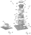
- a capacitive sensing knob 10 comprises a cylindrical sensor arrangement 11 of strip shaped sensor electrodes 13, which is connected to a circuit board 12.
- the sensor electrodes 13 are also known as sensor surfaces 13.
- a cylindrical rotary knob guide 14 is arranged concentrically around the cylindrical sensor arrangement 11.
- Rounded latch protrusions 16 are provided at a bottom circumference of the cylindrical rotary knob guide.
- a tooth gear 17 is provided at the outside of the cylindrical knob guide 14.
- the tooth gear 17 is in contact with a disk shaped encoder gear 18, which is supported on an encoder 19 on the circuit board 12.
- a cylindrical rotary knob grip 20 is arranged concentrically around the cylindrical knob guide 14.
- the cylindrical knob grip 20 comprises a lower rim 15 that protrudes to the outside and an upper rim 9 that protrudes to the inside.
- a cover ring 23 is supported on the lower rim 15 of the cylindrical knob guide. The cover ring 23 fits into a cylindrical opening of a front plate 21.
- a cylindrical centre button reflector 22 is arranged concentrically inside of the cylindrical sensor arrangement 11, of the rotary knob guide 14 and of the rotary knob grip 20.
- An upper rim 24 of the centre button reflector 22, which projects to the outside, comprises four catches 15 that are arranged equidistantly on the upper rim 24.
- a centre button cap 26 is provided on top of the centre button holder 24. The centre button cap 26 comprises a lower rim 27 that fits into the catches 25 of the centre button reflector 22.
- the cylindrical sensor arrangement 11 is provided by a double shot plastic part, which comprises a platable portion and a non-platable portion.
- a double shot plastic part refers to a plastic part that is produced by a double shot injection moulding process.
- the sensor electrodes 13 and electrical connections to the sensor electrodes 13 are provided on the platable portion and non-conducting connecting regions between the sensor electrodes, which form a scaffold for the sensor electrodes, are provided on the non-platable portion.
- the platable portion is plated with a conducting material, such as chrome.
- the platable portion may also be plated with any other material that is applied in a metallization process, such as electroless plating or galvanic plating.
- electroless plating is also known as chemical or autocatalytic plating and the galvanic plating is also known as electroplating.
- the sensor electrodes 13 of the cylindrical sensor arrangement are generated by masking out nonsensor areas of a plastic part, removing the masking substance and plating of the remaining areas.
- a photoactivatable plastic may be used which becomes platable after illumination with light of a suitable wavelength.
- a mask may be used to selectively illuminate portions of the plastic part.
- a production method for a capacitive sensor arrangement according to the application is often cheaper to realize than providing an elastic foil with sensor electrodes. This applies especially in situations in which capacitive sensors are provided on curved or otherwise protruding surfaces such as cylinders, pyramids, wedges etc.
- a first shot comprises a non-platable material, such as polycarbonate
- a second shot comprises a platable grade material, such as Polycarbonate/Acrylnitryle-Butadien-Styrol (PC/ABS) doped with palladium, which forms the base for the capacitive sensors.
- PC/ABS Polycarbonate/Acrylnitryle-Butadien-Styrol
- the surface of the platable second shot material is activated.
- the sensor electrodes are metallized with electroless copper plating.
- the copper may be further covered with a electroless nickel immersion gold (ENIG) plating, wherein the surface is activated with the a solution of a noble metal such as palladium chloride.
- ENIG electroless nickel immersion gold
- a production process for a cylindrical capacitive sensor comprises 1-shot injection moulding and laser activation.
- a doped thermoplastic is injection moulded.
- a laser beam activates the thermoplastic, which is doped with an additive.
- Metallic nuclei are formed which act as a catalyst for reductive copper plating.
- the laser also creates a microscopically rough surface in which copper is kept in place during metallization.
- a step of metallization comprises a cleaning step and a plating step that comprises plating with electroless copper baths.
- the copper surface is plated with a cover metal such as nickel, gold, Sn, Ag, Pd/Au, an organic solderable preservative (OSP) or others.
- OSP organic solderable preservative
- the centre button reflector 22 rests on the rotary knob guide 14.
- the centre button reflector 22 and the lower rim 27 of the centre button cap 26 are covered by the rotary knob grip 20.
- the sensor electrodes 13 of the cylindrical sensor array 11 are connected to an evaluation unit via connecting lines.
- the connecting lines and the evaluation unit are not shown in Figs. 1 and 2 .
- the centre button reflector 22 reflects the light of a lamp that is not shown in Figs. 1 and 2 .
- the lamp may be placed inside of the centre button reflector and reflect light through the centre button cap 26.
- the rotary knob guide 14 If the rotary knob grip 20 is turned, the rotary knob guide 14, the centre button reflector 22 and the centre button cap rotate together with the rotary knob grip 20 against the cylindrical sensor array 11, which is stationary with respect to the circuit board 12.
- the gear 17 turns the encoder gear 18 and the encoder 19 generates an electric signal, which depends on the movement of the gear 17.
- a voltage of the individual sensor electrodes 13 of the cylindrical sensor arrangement 11 is measured by the evaluation unit. If a conducting object, an electrically charged object or an object with dielectric properties approaches the rotary knob grip 20, an electric field between the object and adjacent sensors 11 and a charge on the adjacent sensors 11 changes. The change of charge causes a change in voltage which is detected by the evaluation unit. In this way, the evaluation unit can detect the presence of the object. By evaluating the detected voltage pattern, the evaluation can also detect the presence of several objects and the movement of those objects. In particular, the objects can be fingers of the hand of a user.
- the evaluation unit together with the sensors connected to it, such as the sensors 11, forms a human machine interface (HMI).
- HMI human machine interface
- a detection of fingers of a user can trigger various functions such as an illumination of a unit, switching to a menu screen that is useful for the user or for others.
- the evaluation unit may also detect motion patterns of the fingers such as a click, a double-click or movement of the fingers relative to each other and attribute special functions to the motion patterns.
- One such motion pattern could be generated by keeping the thumb in position while moving another finger around the rotary button grip 20 or away and towards the rotary button grip 20.
- the turning motion can be used for manual browsing through the available frequencies, a click movement could be used to stop and start a frequency sweep and another motion could be used for saving and deleting stored frequencies of radio stations.
- a relative movement of the fingers can be used to adjust a loudspeaker volume while other finger movements can be used to switch to and from various modes such as a traffic message mode, a loudspeaker volume distribution etc.
- various methods may be used to measure a charge on the capacitor surfaces.
- a relaxation oscillator is used.
- a current versus voltage phase shift measurement a resistorcapacitor charge timing, a capacitive bridge divider, a charge transfer, a successive approximation, sigma-delta modulators, charge-accumulation circuits, a field effect, a mutual capacitance, or a frequency shift may be used.
- the capacitive sensor array can be configured to detect if a passenger of a car is wearing gloves and, in this case, the sensitivity of the sensor array is increased, for example by increasing an alternating current detection signal that is fed to a capacitor electrode 13.
- the glove detection may be dependent on a temperature signal from an interior temperature sensor. For example, a glove detection may be made active for cold temperatures only.
- capacitors of the cylindrical capacitive sensor arrangement may be connected in various ways.
- capacitors are formed by two adjacent capacitor surfaces. One of the adjacent capacitor surfaces of a capacitor is connected to a ground potential while the other one of the adjacent capacitor surfaces is connected to a voltage measuring input of a microprocessor.
- a switch such as a semiconductor switch may be provided for connecting different capacitor surfaces to the same voltage measuring input. In this way, a number of voltage measuring inputs of a microprocessor can be made smaller than a number of capacitors of the cylindrical capacitive sensor array. Capacity measurements of the capacitors are then performed by scanning the capacitors in turn using the switch.
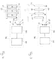
- Figs. 3 and 4 show different circuit layouts for the capacitive sensing knob 10. For simplicity, only a small number of capacitor electrodes is shown in Figs. 3 and 4 .
- the ground-connected capacitor electrodes are separately connected to lines on the circuit board 12, which are connected to a ground potential.
- the first embodiment has the advantage that fewer connection lines are required on the circuit board 12.
- the second embodiment allows to determine the wiring of the capacitor by the design of the circuit board 12 or even to change the wiring dynamically by actuating switches on the circuit board 12.
- Electrode contacts 56, 57, 58, 59 are provided for connecting the sensing electrodes 29, 31 and the ground electrodes 28, 30 to the circuit board 12.
- Fig. 3 shows an electric circuit, which comprises a capacitive sensing similar to the one shown in Fig. 2 .
- Fig. 3 shows four adjacent sensor electrodes 28, 29, 30, 31.
- the sensor electrodes 28, 29, 30, 31 correspond to capacitor plates of three capacitors that comprise the sensor electrodes 28 and 29, 29 and 30, and 30 and 31, respectively. Furthermore, they correspond to the sensor electrodes 13 of Fig. 2 . Capacities between the sensor electrodes 13 are symbolized by capacitor symbols in Fig. 3 .
- the arrangement of sensor electrodes 13 is circular, such that sensor electrode 31 is adjacent to sensor electrode 28 and a fourth capacitor is formed between the sensor electrodes 31 and 28.
- the sensor electrodes are alternately connected to ground and to a voltage sensing input of a capacitance sensing device 32. Every second sensor electrode 29, 31 is connected to a separate voltage sensing input 68, 69 of the capacitance sensing device 32 while the ground potential is connected to a reference input 70 of the capacitance sensing device 32.
- the sensing input and the reference input are also referred to as interface ports.
- the sensor electrode 29 is connected to voltage sensing input 29 and the sensor electrode 31 is connected to voltage sensing input 34 of the capacitance sensing device 32.
- the capacitance sensing device 32 is connected to a decision logic 35 which is arranged together with the capacitance sensing device 32 on a printed circuit board 36.
- a current signal is provided to a capacitor electrode via one of the voltage sensing inputs. After providing the current signal, a response signal is detected at the voltage sensing input.
- the decision logic 35 evaluates the change in capacitance and determines a finger distance and/or position.
- Fig. 4 shows a second layout in which reference electrodes, which are connected to ground potential, are connected with each other on a plastic part. Similar to Fig. 3 , the reference electrodes are arranged between sensing electrodes, which are electrically isolated to each other and to the ground potential.
- the ground-connected capacitor electrodes are connected among each other to a compound ground electrode 67, for example by a conductive part of the plastic part or by a conductive strip.
- the compound ground electrode 67 is connected via an electrode contact 68 to a connection line on the circuit board 12 that is connected to a ground potential.
- Further electrode contacts 60, 61, 62 are provided for connecting the sensing electrodes 60, 61, 62 to the circuit board.
- a further contact 63 is provided for connecting the compound ground electrode 67 to the capacitance sensing device 32.
- the compound ground electrode may be grounded via the capacitance sensing device 32.
- the contact 68 may be omitted.
- the compound ground electrode 67 and the capacitance sensing device 32 are separately grounded.
- the contact 63 may be omitted. Similar alternatives apply to the embodiment of Fig. 3 .
- sensor electrodes 64 are connected to sensing inputs 71, 72, 73 and the compound ground electrode is connected to a reference input 74.
- Fig. 5 shows a perspective sectional view of a bottom region of the capacitive sensing knob.
- the sensor electrodes 13 are mounted on the plated portion of front plate 21.
- the contacts are heat staked or otherwise mounted and electrically connected to the front plate.
- the contact springs 38 provide a means for balancing out tolerances and height differences.
- a circular latch spring 39 is provided below the latch feet 16.
- the circular latch spring 39 is attached to the circuit board 12, either directly or indirectly via a cylindrical casing which is not shown in Fig. 1 .
- the attachment of the circular latch spring 39 is shown as a screw connection.
- the circular latch spring 39 engages into spaces between the latch feet 16.
- the capacitive sensing knob 10 takes on one of several latch positions when it is not turned.
- the capacitive sensing knob 10 is not moved out of position by vibrations of an automobile.
- a user needs to overcome a spring resistance to move the capacitive sensing knob 10 from one latch position to an adjacent latch position.
- the circular latch spring 39 provides a haptic feedback to the user and a better control of the turning angle. This can be useful for a tuning knob of a car radio, for example.
- the haptic feedback is provided by a circular plastic part with a surface form that matches the latch feet 16. This plastic part is pressed toward the latch feet 16 from the circuit board 12 with a spring. In this way, the spring does not need to match the form of the latch feet and a lasting deformation of the spring affects the function only marginally.
- Fig. 6 shows a top view of a bottom section of the capacitive sensing knob 10. For clarity, relative radial distances have been exaggerated in Fig. 5 .
- a short-circuit spring 40 which is made of a conducting material, is attached to an inner wall of the rotary knob guide 14.
- the dimension of the short-circuit spring 40 is made such that, in one of several pre-determined positions, a first portion of the short circuit spring touches a first sensor electrode 13 and a second portion of the short-circuit spring touches a second electrode 13.
- the height of the short-circuit spring 40 is made smaller than the distance between two adjacent electrodes 13 such that the location of a finger which is placed on an outer surface of the rotary knob grip 15.
- a latch spring 41 may be provided on the inner wall of the rotary knob guide 14.
- the dimension of the latch spring 41 is made such that, in one of the several predetermined positions, a first portion of the latch spring 41 engages between an interstice between two adjacent sensor electrodes 13 and a second portion of the latch spring 41 engages into an interstice between two adjacent sensor electrodes 13.
- the latch spring 41 need not contain conducting material.
- the latch spring 41 may be provided in addition to the circular latch spring 39 of Fig. 4 or instead of the circular latch spring 39.
- two adjacent electrode surfaces 13 are short circuited when the capacitive sensing knob reaches one of the pre-determined positions. Thereby, the adjacent electrode surfaces 13 are forced onto the same electric potential. Especially for a circuit layout in which every second electrode surface is connected to ground potential, the two adjacent electrode surfaces 13 take on ground potential.
- the capacitance sensing device 32 detects which pair of adjacent electrode surfaces are on the same potential and the decision logic 35 uses this information to compute an angular position of the capacitive sensing knob 10.
- a finger detection is triggered if a potential difference between ground and a sensing electrode is between a predetermined minimum value and a pre-determined maximum value and no finger touch signal is triggered otherwise.
- an evaluation method may differentiate between an intentional contact of the capacitive sensing button and an unintentional contact. This discernment may be done based on the number of detected fingers and/or on the length of the contact. By way of example, a contact with the capacitive sensing knob 10 may be classified as intentional when the number of finger detections is between 2 and 4 and as unintentional otherwise.
- Fig. 7 shows further types of position sensors 42, 43, 44 for use with the capacitive sensor array 11.
- the position sensors comprise an inductive sensor 42, light sensor 43 with a photodiode and a photo element and a capacitive sensor 44. Similar to Fig. 6 , the position sensors 42, 43, 44 are placed at an inner wall of the rotary knob guide 14.
- the sensor are 42, 43, 44 work contactless, but they require a separate current supply to the rotating rotary knob guide 14. A separation is provided between the light source and the photodiode to provide a direct illumination of the photodiode.
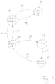
- Fig. 8 shows a state diagram of the capacitive sensing knob 10.
- an off state 45 a system, such as the air conditioning or the car radio, is switched off.
- the system changes to a standby state 46 through transition 47.
- the standby state 46 a system display is off or is dimmed. If an intentional finger contact is detected, the system changes via transition 50 from the standby state 46 into an active state 49, in which the display is lighted. After a pre-determined period of receiving no commands, the system changes back from the active state 49 into the standby state 46 via transition 51.
- the system receives further sensor signals in the active state 49 it changes into a scanning state 50 via transition 52.
- the scanning state 50 the system scans a motion of the capacitive sensing knob 10, for example by tracing a moving short circuit, wherein the short circuit is caused by a pre-determined position the short circuit spring.
- a command signal such as a knob rotation or a pre-determined finger contact pattern is detected, the system changes via transition 54 into a command execution state 53, in which system parameters, such as a radio loudness or frequency, are adjusted. After adjusting the parameters, the system changes back into the active mode 49 via transition 55.
Description
- Capacitive sensing devices for detecting the position of a hand are commonly used in touch screens. A touchscreen panel comprises an insulator such as glass, which is coated with a transparent conductor such as indium tin oxide (ITO). As the human body is also an electrical conductor, touching the surface of the screen results in a distortion of the screen's electrostatic field, measurable as a change in capacitance. Different technologies may be used to determine the location of the touch. The location is then sent to a controller for processing.
-
US 2008/111428 A1 discloses a motion detecting device according to the preamble of the independent claim. - It is an object of the present application to provide an improved capacitive sensor arrangement.
- The application discloses a motion detecting device which comprises a stationary plastic sensor carrier, which is stationary with respect attachment regions for attachment to a base plate. The stationary plastic sensor carrier comprises two sensor carrier sections and an insulation section. The carrier section comprises a first plastic material and the insulation section comprises a second plastic material. The insulation section extends between two adjacent sensor carrier sections and the sensor carrier sections and the at least one insulation section are integrally formed by a plastic moulding process.
- Plated metal sensing surfaces are provided on the surfaces of the sensor carrier sections. Surface electrode contacts are provided for connecting the plated metal surface electrodes with a PCB. Thereby they define at least one capacitive area between at least two of the plated metal surface electrodes. A plastic knob element is movably arranged on the plastic sensor carrier, such that the insulating plastic separator sections and the plated metal sensing surface electrodes are at least partly covered by the knob element.
- The motion detecting device comprises a short circuit spring that is attached to the plastic knob element. Two portions of the short circuit spring form a short circuit between two electrode surfaces in a first predefined position or positions and wherein the two portions of the short circuit spring do not form a short circuit between any electrode surfaces in a second predefined position or positions. In this way, a position of the plastic knob element can be determined easily just by evaluating a voltage potential of the electrode surfaces and without the need of a further sensor.
- Advantageously, the surface electrodes are subdivided into a sensing set of surface electrodes which are electrically isolated against each other and a reference set of surface electrodes which are electrically connected to each other. The electrical connection of the reference set may also be provided on a printed circuit board on which the motion detecting device is mounted.
- By using a plastic sensor carrier according to the application, sensor electrodes can be produced efficiently and in a cost saving manner. In particular, this applies to three dimensional arrangements of sensor electrodes. In one embodiment, the sensor carrier sections and the insulation section are formed by a time saving and inexpensive double shot injection moulding process.
- The plated metal surface electrodes may comprise a copper plating for providing good conductivity. Additionally the plated metal surface electrodes may comprises a protective cover metal such as nickel. For better protection, the metal surface electrodes may also comprises an electroless nickel immersion gold plating and or and organic solderable preservative.
- The at least two carrier sections may comprise Acrylnitryle-Butadien-Styrole which is durable and can be plated with electric or electroless plating, especially after preparation with an acid.
- According to the application, various means may be provided for determining a position, such as an angular positioning, of the plastic knob element.
- According to a further modification, the motion detecting device comprises a light sensor with a light source, such as an LED or a light bulb, and a light detector. The light source is attached to the plastic knob element, and the light source is mounted such that it illuminates an electrode surface in a predetermined position. The light detector is mounted such that it receives reflected light from the electrode surface in the predetermined position. Thereby, a position of the plastic knob element can be determined with a contactless sensor.
- According to another modification, the motion device comprises an inductive sensor with a magnet and a coil. The magnet and the coil are attached to the plastic knob element. The magnet may be provided by a permanent magnet, by the aforementioned coil or by a second coil. Thereby, a position of the plastic knob element can be determined with a contactless sensor.
- Furthermore, the motion device may comprise a gear wheel at the outside of the plastic knob element, which provided for engagement with a sensor gear wheel on a circuit board on which the motion device is mounted. The gear wheel is arranged at an outer wall of the rotary knob guide and close to a bottom surface of the rotary knob guide.
- In a particular embodiment, the outer shape of the motion detecting device is designed as a protrusion with a conical shape, a frustoconical shape, a pyramidal shape or a truncated pyramid shape. The cone may have a polygonal cross section or a curved cross section or a combination of both wherein the outer boundary of the cross section comprises one or more curved lines and one or more straight lines. Such a design can facilitate a handling of the motion detecting device with the hand and can also provide a haptic feedback about the orientation of the motion detecting device.
- In a further modification, the plastic knob element comprises a knob guide and a knob grip, wherein the knob grip is arranged on the knob guide. Thereby, the knob guide and the interior of the knob guide can be protected from adverse influences such as dust and liquids. The knob guide may furthermore comprise a tooth gear for engagement with a wheel.
- In a further modification, a centre button reflector is arranged inside the plastic knob element and an at least partially light transmissive centre button cap is provided on top of the plastic knob element. Thereby, the plastic knob element can be lighted for easier orientation in the dark. The reflector helps to direct the light of an illumination at a bottom of the plastic knob element to the button cap. Especially, the lighting may be turned on when a key of a car is turned into a predetermined position.
- The application furthermore discloses a motion detection interface arrangement with the abovementioned motion detecting device. The motion detection interface arrangement comprises a circuit board such as a printed circuit board with conductive paths. The conductive paths are connected to interface ports which are electrically connected to the surface electrode contacts.
- In a further embodiment, the motion detection interface arrangement comprises a latching spring, which is attached to the PCB, and a plurality of protrusions at a bottom end of the plastic knob element, wherein the latching spring engages between at least two of the protrusions. The latching spring holds the plastic knob element in a defined position and provides a haptic feedback to a user of the knob element.
- In another embodiment, the motion detection interface arrangement comprises a latching spring, a latching element and a plurality of protrusions at a bottom end of the plastic knob element. The latching spring is attached to the PCB and the latching element is arranged between the protrusion and the latching spring. The latching element engages between at least two of the protrusions. By providing a latching element which is not easily deformed, the latching mechanism can be made durable.
- Furthermore, the motion detection interface arrangement may comprise a wheel that is mounted on the PCB and a detecting means for detecting a motion of the wheel, the wheel engaging with a gear on the knob element and the detecting means being electrically connected to a conductive path on the PCB.
- The application furthermore discloses motion detection device with the abovementioned motion detection arrangement and with an electronic evaluation unit having a plurality of interface ports. The interface ports are electrically connected with the conductive paths of the PCB. The electronic evaluation unit comprises means to evaluate a state of the surface electrodes. Furthermore, it may also comprise means of sending a probe signal to the surface electrodes.
- In particular, the electronic evaluation unit may comprise means for detecting an intentional hand contact by evaluating the strength and duration of signals from the electrode surfaces via the interface ports. Furthermore, the electronic evaluation unit may comprise means for detecting a finger position by evaluating signals from the electrode surfaces via the interface ports.
- Moreover, the electronic evaluation unit may comprise means for detecting if a hand is covered by a material, for example a glove, by evaluating the strength of signals from the electrode surfaces via the interface ports during an approach of the hand and during the hand contact. The approach and the contact are detected by the time dependence and pattern of the signals. This is especially advantageous in a passenger compartment of a car during winter.
- Moreover, the electronic evaluation unit may comprise mean for detecting a rotational position of the knob element by detecting a short circuit between two of the electrode surfaces and by detecting the absence of a short circuit between electrode surfaces. The short circuit may be detected by measuring a voltage difference, for example.
- Moreover, the electronic evaluation unit may comprise means for detecting a rotational position of the knob element by evaluating an electric signal from a coil via conductive paths of the PCB, wherein the coil is attached to the knob element.
- Moreover, the electronic evaluation unit may comprise mean for detecting a rotational position of the knob element by evaluating an electric signal from a light detector via conductive paths of the PCB, the light detector being attached to the knob element.
- Furthermore, the application discloses a vehicle, especially a motorized vehicle such as a passenger car, with the above-mentioned motion detection device, wherein the motion detection device is integrated into an operating panel that is provided in a passenger compartment of the vehicle. the electronic evaluation unit of the motion detection device is electrically connected to a device of the vehicle, such as a climatization device, a passenger information and/or entertainment device, a window lifter, rear mirror adjustment device, a sliding roof motor etc.
- Furthermore, the application discloses a method for producing a cylindrical capacitive sensor arrangement. A first shot moulded plastic part is injection moulded. A platable plastic material is provide and a second shot moulded plastic part is injection moulded from the platable plastic material. The second shot moulded plastic part is plated in a metallization step. Therein, the mould form for moulding the second shot moulded plastic part is designed such that the second shot moulding part comprises strip shaped platable regions. Electrical contacts to the strip shaped platable regions are formed. In particular, the strip shaped regions may be aligned parallel to a symmetry axis of a cylinder. The injection moulding of the first shot moulded plastic part and the second shot moulded plastic part may be performed simultaneously or also one after the other.
- The application is now explained in further detail with respect to the following Figures in which
- Figure 1
- shows a capacitive sensing knob according to the application, and
- Figure 2
- shows an exploded view of the capacitive sensing knob of
Fig. 1 , - Figure 3
- shows an electric circuit of the capacitive sensing knob of
Fig. 2 , - Figure 4
- shows a second electric circuit layout of the capacitive sensing knob of
Fig. 2 , - Figure 5
- shows a partial view of a bottom portion of the capacitive sensing knob,
- Figure 6
- shows a cross section through the capacitive sensing knob,
- Figure 7
- shows various position sensors for use with the capacitor arrangement of
Fig. 2 , and - Figure 8
- shows a state diagram for the capacitive sensing knob.
- In the following description, details are provided to describe the embodiments of the application. It shall be apparent to one skilled in the art, however, that the embodiments may be practised without such details.
- A
capacitive sensing knob 10 according to the application comprises a cylindrical sensor arrangement 11 of strip shapedsensor electrodes 13, which is connected to a circuit board 12. Thesensor electrodes 13 are also known as sensor surfaces 13. A cylindricalrotary knob guide 14 is arranged concentrically around the cylindrical sensor arrangement 11.Rounded latch protrusions 16 are provided at a bottom circumference of the cylindrical rotary knob guide. - A tooth gear 17 is provided at the outside of the
cylindrical knob guide 14. The tooth gear 17 is in contact with a disk shaped encoder gear 18, which is supported on anencoder 19 on the circuit board 12. A cylindricalrotary knob grip 20 is arranged concentrically around thecylindrical knob guide 14. Thecylindrical knob grip 20 comprises alower rim 15 that protrudes to the outside and an upper rim 9 that protrudes to the inside. Acover ring 23 is supported on thelower rim 15 of the cylindrical knob guide. Thecover ring 23 fits into a cylindrical opening of a front plate 21. - A cylindrical
centre button reflector 22 is arranged concentrically inside of the cylindrical sensor arrangement 11, of therotary knob guide 14 and of therotary knob grip 20. An upper rim 24 of thecentre button reflector 22, which projects to the outside, comprises fourcatches 15 that are arranged equidistantly on the upper rim 24. Acentre button cap 26 is provided on top of the centre button holder 24. Thecentre button cap 26 comprises a lower rim 27 that fits into the catches 25 of thecentre button reflector 22. - In the embodiment of
Figs. 1 and 2 , the cylindrical sensor arrangement 11 is provided by a double shot plastic part, which comprises a platable portion and a non-platable portion. Herein, a double shot plastic part refers to a plastic part that is produced by a double shot injection moulding process. In particular, thesensor electrodes 13 and electrical connections to thesensor electrodes 13 are provided on the platable portion and non-conducting connecting regions between the sensor electrodes, which form a scaffold for the sensor electrodes, are provided on the non-platable portion. - The platable portion is plated with a conducting material, such as chrome. Alternatively, the platable portion may also be plated with any other material that is applied in a metallization process, such as electroless plating or galvanic plating. In the art, the electroless plating is also known as chemical or autocatalytic plating and the galvanic plating is also known as electroplating.
- In a one embodiment, the
sensor electrodes 13 of the cylindrical sensor arrangement are generated by masking out nonsensor areas of a plastic part, removing the masking substance and plating of the remaining areas. Herein, a photoactivatable plastic may be used which becomes platable after illumination with light of a suitable wavelength. Instead of a masking substance, a mask may be used to selectively illuminate portions of the plastic part. - A production method for a capacitive sensor arrangement according to the application is often cheaper to realize than providing an elastic foil with sensor electrodes. This applies especially in situations in which capacitive sensors are provided on curved or otherwise protruding surfaces such as cylinders, pyramids, wedges etc.
- In a double-shot moulding production process according to the application, a first shot comprises a non-platable material, such as polycarbonate, and a second shot comprises a platable grade material, such as Polycarbonate/Acrylnitryle-Butadien-Styrol (PC/ABS) doped with palladium, which forms the base for the capacitive sensors. During a chromic acid etching step, the surface of the platable second shot material is activated. In a metallization step, the sensor electrodes are metallized with electroless copper plating. The copper may be further covered with a electroless nickel immersion gold (ENIG) plating, wherein the surface is activated with the a solution of a noble metal such as palladium chloride.
- According to another embodiment, a production process for a cylindrical capacitive sensor comprises 1-shot injection moulding and laser activation. In a moulding step, a doped thermoplastic is injection moulded. In a step of laser activation, a laser beam activates the thermoplastic, which is doped with an additive. Metallic nuclei are formed which act as a catalyst for reductive copper plating. The laser also creates a microscopically rough surface in which copper is kept in place during metallization. A step of metallization comprises a cleaning step and a plating step that comprises plating with electroless copper baths. In a finishing step, the copper surface is plated with a cover metal such as nickel, gold, Sn, Ag, Pd/Au, an organic solderable preservative (OSP) or others.
- In the assembled state shown in
Fig. 1 , thecentre button reflector 22 rests on therotary knob guide 14. Thecentre button reflector 22 and the lower rim 27 of thecentre button cap 26 are covered by therotary knob grip 20. Thesensor electrodes 13 of the cylindrical sensor array 11 are connected to an evaluation unit via connecting lines. The connecting lines and the evaluation unit are not shown inFigs. 1 and 2 . During operation, thecentre button reflector 22 reflects the light of a lamp that is not shown inFigs. 1 and 2 . For example, the lamp may be placed inside of the centre button reflector and reflect light through thecentre button cap 26. - If the
rotary knob grip 20 is turned, therotary knob guide 14, thecentre button reflector 22 and the centre button cap rotate together with therotary knob grip 20 against the cylindrical sensor array 11, which is stationary with respect to the circuit board 12. The gear 17 turns the encoder gear 18 and theencoder 19 generates an electric signal, which depends on the movement of the gear 17. - Furthermore, a voltage of the
individual sensor electrodes 13 of the cylindrical sensor arrangement 11 is measured by the evaluation unit. If a conducting object, an electrically charged object or an object with dielectric properties approaches therotary knob grip 20, an electric field between the object and adjacent sensors 11 and a charge on the adjacent sensors 11 changes. The change of charge causes a change in voltage which is detected by the evaluation unit. In this way, the evaluation unit can detect the presence of the object. By evaluating the detected voltage pattern, the evaluation can also detect the presence of several objects and the movement of those objects. In particular, the objects can be fingers of the hand of a user. - The evaluation unit together with the sensors connected to it, such as the sensors 11, forms a human machine interface (HMI). According to the application, a detection of fingers of a user can trigger various functions such as an illumination of a unit, switching to a menu screen that is useful for the user or for others.
- The evaluation unit may also detect motion patterns of the fingers such as a click, a double-click or movement of the fingers relative to each other and attribute special functions to the motion patterns. One such motion pattern could be generated by keeping the thumb in position while moving another finger around the
rotary button grip 20 or away and towards therotary button grip 20. - Especially in an automotive environment, it can be advantageous to provide a button with multiple functions. Thereby, it is possible for a driver to keep the hand in one location while operating the various functions. Especially for a tuning button of a car radio, the turning motion can be used for manual browsing through the available frequencies, a click movement could be used to stop and start a frequency sweep and another motion could be used for saving and deleting stored frequencies of radio stations. A relative movement of the fingers can be used to adjust a loudspeaker volume while other finger movements can be used to switch to and from various modes such as a traffic message mode, a loudspeaker volume distribution etc.
- According to the application, various methods may be used to measure a charge on the capacitor surfaces. In one embodiment, a relaxation oscillator is used. In other embodiments, a current versus voltage phase shift measurement, a resistorcapacitor charge timing, a capacitive bridge divider, a charge transfer, a successive approximation, sigma-delta modulators, charge-accumulation circuits, a field effect, a mutual capacitance, or a frequency shift may be used.
- In a glove detection mode, the capacitive sensor array can be configured to detect if a passenger of a car is wearing gloves and, in this case, the sensitivity of the sensor array is increased, for example by increasing an alternating current detection signal that is fed to a
capacitor electrode 13. The glove detection may be dependent on a temperature signal from an interior temperature sensor. For example, a glove detection may be made active for cold temperatures only. - The capacitor electrodes of the cylindrical capacitive sensor arrangement may be connected in various ways. In one embodiment, capacitors are formed by two adjacent capacitor surfaces. One of the adjacent capacitor surfaces of a capacitor is connected to a ground potential while the other one of the adjacent capacitor surfaces is connected to a voltage measuring input of a microprocessor. Alternatively, a switch such as a semiconductor switch may be provided for connecting different capacitor surfaces to the same voltage measuring input. In this way, a number of voltage measuring inputs of a microprocessor can be made smaller than a number of capacitors of the cylindrical capacitive sensor array. Capacity measurements of the capacitors are then performed by scanning the capacitors in turn using the switch.
-
Figs. 3 and 4 show different circuit layouts for thecapacitive sensing knob 10. For simplicity, only a small number of capacitor electrodes is shown inFigs. 3 and 4 . - In a first embodiment, which is shown in
Fig. 3 , the ground-connected capacitor electrodes are separately connected to lines on the circuit board 12, which are connected to a ground potential. The first embodiment has the advantage that fewer connection lines are required on the circuit board 12. The second embodiment, on the other hand, allows to determine the wiring of the capacitor by the design of the circuit board 12 or even to change the wiring dynamically by actuating switches on the circuit board 12. -
Electrode contacts sensing electrodes 29, 31 and theground electrodes -
Fig. 3 shows an electric circuit, which comprises a capacitive sensing similar to the one shown inFig. 2 . By way of example,Fig. 3 shows fouradjacent sensor electrodes sensor electrodes sensor electrodes sensor electrodes 13 ofFig. 2 . Capacities between thesensor electrodes 13 are symbolized by capacitor symbols inFig. 3 . The arrangement ofsensor electrodes 13 is circular, such that sensor electrode 31 is adjacent tosensor electrode 28 and a fourth capacitor is formed between thesensor electrodes 31 and 28. - In the arrangement of
Fig. 3 , the sensor electrodes are alternately connected to ground and to a voltage sensing input of a capacitance sensing device 32. Everysecond sensor electrode 29, 31 is connected to a separatevoltage sensing input reference input 70 of the capacitance sensing device 32. The sensing input and the reference input are also referred to as interface ports. - In particular, the
sensor electrode 29 is connected tovoltage sensing input 29 and the sensor electrode 31 is connected tovoltage sensing input 34 of the capacitance sensing device 32. The capacitance sensing device 32 is connected to adecision logic 35 which is arranged together with the capacitance sensing device 32 on a printedcircuit board 36. - During a capacitance measurement, a current signal is provided to a capacitor electrode via one of the voltage sensing inputs. After providing the current signal, a response signal is detected at the voltage sensing input. The
decision logic 35 evaluates the change in capacitance and determines a finger distance and/or position. -
Fig. 4 shows a second layout in which reference electrodes, which are connected to ground potential, are connected with each other on a plastic part. Similar toFig. 3 , the reference electrodes are arranged between sensing electrodes, which are electrically isolated to each other and to the ground potential. - In the embodiment of
Fig. 4 , the ground-connected capacitor electrodes are connected among each other to acompound ground electrode 67, for example by a conductive part of the plastic part or by a conductive strip. Thecompound ground electrode 67 is connected via anelectrode contact 68 to a connection line on the circuit board 12 that is connected to a ground potential. Further electrode contacts 60, 61, 62 are provided for connecting the sensing electrodes 60, 61, 62 to the circuit board. Afurther contact 63 is provided for connecting thecompound ground electrode 67 to the capacitance sensing device 32. - In a modified embodiment, the compound ground electrode may be grounded via the capacitance sensing device 32. In this case, the
contact 68 may be omitted. In a further modification, thecompound ground electrode 67 and the capacitance sensing device 32 are separately grounded. In this case, thecontact 63 may be omitted. Similar alternatives apply to the embodiment ofFig. 3 . - Similar to the embodiment of
Fig. 3 ,sensor electrodes 64 are connected to sensinginputs 71, 72, 73 and the compound ground electrode is connected to a reference input 74. -
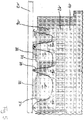
Fig. 5 shows a perspective sectional view of a bottom region of the capacitive sensing knob. Thesensor electrodes 13 are mounted on the plated portion of front plate 21. The contacts are heat staked or otherwise mounted and electrically connected to the front plate. The contact springs 38 provide a means for balancing out tolerances and height differences. Acircular latch spring 39 is provided below thelatch feet 16. Thecircular latch spring 39 is attached to the circuit board 12, either directly or indirectly via a cylindrical casing which is not shown inFig. 1 . By way of example, the attachment of thecircular latch spring 39 is shown as a screw connection. - In a latch position of the
capacitive sensing knob 10, thecircular latch spring 39 engages into spaces between thelatch feet 16. Thereby, thecapacitive sensing knob 10 takes on one of several latch positions when it is not turned. In particular, thecapacitive sensing knob 10 is not moved out of position by vibrations of an automobile. A user needs to overcome a spring resistance to move thecapacitive sensing knob 10 from one latch position to an adjacent latch position. Thereby, thecircular latch spring 39 provides a haptic feedback to the user and a better control of the turning angle. This can be useful for a tuning knob of a car radio, for example. - In a further embodiment, the haptic feedback is provided by a circular plastic part with a surface form that matches the
latch feet 16. This plastic part is pressed toward thelatch feet 16 from the circuit board 12 with a spring. In this way, the spring does not need to match the form of the latch feet and a lasting deformation of the spring affects the function only marginally. -
Fig. 6 shows a top view of a bottom section of thecapacitive sensing knob 10. For clarity, relative radial distances have been exaggerated inFig. 5 . - A short-circuit spring 40, which is made of a conducting material, is attached to an inner wall of the
rotary knob guide 14. The dimension of the short-circuit spring 40 is made such that, in one of several pre-determined positions, a first portion of the short circuit spring touches afirst sensor electrode 13 and a second portion of the short-circuit spring touches asecond electrode 13. Advantageously, the height of the short-circuit spring 40 is made smaller than the distance between twoadjacent electrodes 13 such that the location of a finger which is placed on an outer surface of therotary knob grip 15. - Optionally, a
latch spring 41 may be provided on the inner wall of therotary knob guide 14. The dimension of thelatch spring 41 is made such that, in one of the several predetermined positions, a first portion of thelatch spring 41 engages between an interstice between twoadjacent sensor electrodes 13 and a second portion of thelatch spring 41 engages into an interstice between twoadjacent sensor electrodes 13. Different from the short-circuit spring 40, thelatch spring 41 need not contain conducting material. Thelatch spring 41 may be provided in addition to thecircular latch spring 39 ofFig. 4 or instead of thecircular latch spring 39. - During operation, two adjacent electrode surfaces 13 are short circuited when the capacitive sensing knob reaches one of the pre-determined positions. Thereby, the adjacent electrode surfaces 13 are forced onto the same electric potential. Especially for a circuit layout in which every second electrode surface is connected to ground potential, the two adjacent electrode surfaces 13 take on ground potential. The capacitance sensing device 32 detects which pair of adjacent electrode surfaces are on the same potential and the
decision logic 35 uses this information to compute an angular position of thecapacitive sensing knob 10. - According to a further evaluation method of capacitor signals, a finger detection is triggered if a potential difference between ground and a sensing electrode is between a predetermined minimum value and a pre-determined maximum value and no finger touch signal is triggered otherwise. Furthermore, an evaluation method may differentiate between an intentional contact of the capacitive sensing button and an unintentional contact. This discernment may be done based on the number of detected fingers and/or on the length of the contact. By way of example, a contact with the
capacitive sensing knob 10 may be classified as intentional when the number of finger detections is between 2 and 4 and as unintentional otherwise. -
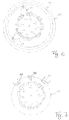
Fig. 7 shows further types ofposition sensors inductive sensor 42,light sensor 43 with a photodiode and a photo element and a capacitive sensor 44. Similar toFig. 6 , theposition sensors rotary knob guide 14. The sensor are 42, 43, 44 work contactless, but they require a separate current supply to the rotatingrotary knob guide 14. A separation is provided between the light source and the photodiode to provide a direct illumination of the photodiode. - By way of example,
Fig. 8 shows a state diagram of thecapacitive sensing knob 10. In an off state 45, a system, such as the air conditioning or the car radio, is switched off. When a car ignition is turned on, the system changes to astandby state 46 through transition 47. When the ignition is turned off, the system changes from thestandby state 46 to the off state 45 through transition 48. In thestandby state 46, a system display is off or is dimmed. If an intentional finger contact is detected, the system changes via transition 50 from thestandby state 46 into an active state 49, in which the display is lighted. After a pre-determined period of receiving no commands, the system changes back from the active state 49 into thestandby state 46 via transition 51. - If the system receives further sensor signals in the active state 49 it changes into a scanning state 50 via transition 52. In the scanning state 50, the system scans a motion of the
capacitive sensing knob 10, for example by tracing a moving short circuit, wherein the short circuit is caused by a pre-determined position the short circuit spring. If a command signal such as a knob rotation or a pre-determined finger contact pattern is detected, the system changes viatransition 54 into a command execution state 53, in which system parameters, such as a radio loudness or frequency, are adjusted. After adjusting the parameters, the system changes back into the active mode 49 via transition 55. - Although the above description contains much specificity, these should not be construed as limiting the scope of the embodiments but merely providing illustration of the foreseeable embodiments. Especially the above stated advantages of the embodiments should not be construed as limiting the scope of the embodiments but merely to explain possible achievements if the described embodiments are put into practise. Thus, the scope of the embodiments should be determined by the claims and their equivalents, rather than by the examples given.
Reference Reference 35 decision logic 36 printed circuit board 10 capacitive sensing knob 37 bottom plates 11 cylindrical sensor arrangement 38 contact spring 39 circular latch spring 12 circuit board 40 short- circuit spring 13 strip shaped sensor electrodes 41 latch spring 42, 43, 44 position sensors 14 cylindrical rotary knob 45 off state guide 46 standby state 15 guiding ring 47 state transition 16 rounded latch feet 48 state transition 17 tooth gear 49 active state 18 disk shaped encoder gear 50 state transition 51 state transition 19 encoder 52 state transition 20 cylindrical rotary knob 53 command execution state grip 54 state transition 21 front plate 55 state transition 22 centre button reflector 56 - 59 electrode contacts 23 cover ring 64 - 67 electrodes 24 upper rim 68 - 70 interface ports 25 catches 71 - 74 interface ports 26 centre button cap 27 lower rim 28 sensor electrode 29 sensor electrode 30 sensor electrode 31 sensor electrode 32 capacitance sensing device 33 voltage sensing input 34 voltage sensing input
Claims (24)
- Motion detecting device (10) comprising- a stationary plastic sensor carrier (11) comprising- at least two sensor carrier sections comprising a first plastic material and at least one insulation section comprising a second plastic material, the at least one insulation section extending between two adjacent sensor carrier sections, the at least two sensor carrier sections and the at least one insulation section being integrally formed by a plastic molding process,- plated metal surface electrodes (13) being provided on the surfaces of the sensor carrier sections,- surface electrode contacts (56 - 59; 60 - 63) for connecting the plated metal surface electrodes (13) with a PCB (12), and- a plastic knob element (14, 20) being movably arranged on the plastic sensor carrier (11), such that the insulating plastic separator sections and the plated metal surface electrodes (13) are at least partly covered by the knob element (14, 20),characterized in that the motion detecting device (10) comprises a short circuit spring (40), the short circuit spring (40) being attached to the plastic knob element, wherein two portions of the short circuit spring (40) form a short circuit between two electrode (13) surfaces in a first predefined position and wherein the two portions of the short circuit spring (40) do not form a short circuit between any electrode (13) surfaces in a second predefined position.
- Motion detecting device (10) according to claim 1,
wherein the sensor carrier sections and the insulation section are formed by a double shot injection moulding process. - Motion detecting device (10) according to claim 1 or claim 2, wherein the plated metal surface electrodes (13) comprise a copper plating.
- Motion detecting device (10) according to one of the preceding claims, wherein the plated metal surface electrodes (13) comprise a nickel plating.
- Motion detecting device (10) according to one of the preceding claims, wherein the plated metal surface electrodes (13) comprise an electroless nickel immersion gold plating.
- Motion detecting device (10) according to one of the preceding claims, wherein the plated metal surface electrodes (13) comprise an organic solderable preservative.
- Motion detecting device (10) according to one of the preceding claims, wherein the at least two carrier sections comprise Acrylnitryle-Butadien-Styrole.
- Motion detecting device (10) according to one of the preceding claims, wherein the outer shape of the motion detecting device is selected from a conical shape, a frustoconical shape, a pyramidal shape and a truncated pyramid shape.
- Motion detecting device (10) according to one of the preceding claims, the motion detecting device comprising a light sensor with a light source and a light detector, wherein the light source is attached to the plastic knob element, and wherein the light source is mounted such that it illuminates an electrode surface in a predetermined position and the light detector is mounted such that it receives reflected light from the electrode surface in the predetermined position.
- Motion detecting device (10) according to one of the preceding claims, the motion device comprising an inductive sensor, the inductive sensor comprising a magnet and a coil, the magnet and the coil being attached to the plastic knob element.
- Motion detecting device (10) according to one of the preceding claims, the motion detecting device (10) comprising a gear wheel, the gear wheel being provided for engagement with a sensor gear wheel on a circuit board, the gear wheel being arranged at an outer wall of the rotary knob guide.
- Motion detecting device (10) according to one of the preceding claims, wherein the plastic knob element (14, 20) comprises a knob guide (14) and a knob grip (20), wherein the knob grip (20) is arranged on the knob guide (14), and wherein the knob guide comprises a tooth gear (17).
- Motion detecting device (10) according to one of the preceding claims, wherein a centre button reflector (24) is arranged inside the plastic knob element (14, 20), and wherein a centre button cap (26) is provided on top of the plastic knob element (14, 20).
- Motion detection interface arrangement (10) comprising a motion detecting device according to one of the preceding claims and a PCB with conductive paths comprising a plurality of interface ports (68 - 70; 71 - 74), the surface electrode contacts being electrically connected with the interface ports.
- Motion detection interface arrangement (10) according to claim 14, further comprising a latching spring, the latching spring being attached to the PCB, and a plurality of protrusions at a bottom end of the plastic knob element, wherein the latching spring engages between at least two of the protrusions.
- Motion detection interface arrangement (10) according to claim 14, further comprising a latching spring and a latching element and a plurality of protrusions at a bottom end of the plastic knob element, wherein the latching spring is attached to the PCB, the latching element is arranged between the protrusion and the latching spring, and wherein the latching element engages between at least two of the protrusions.
- Motion detection interface arrangement (10) according to one of claims 14 to 16, further comprising a wheel that is mounted on the PCB and a detecting means for detecting a motion of the wheel, the wheel engaging with a gear on the knob element (14, 20) and the detecting means being electrically connected to a conductive path on the PCB.
- Motion detection device comprising a motion detection arrangement according (10) to one of the claims 9 to 13 and an electronic evaluation unit (36) with a plurality of interface ports, wherein the interface ports are electrically connected with the conductive paths of the PCB.
- Motion detection device according to claim 18, wherein the electronic evaluation unit comprises means for detecting an intentional hand contact by evaluating the strength and duration of signals from the electrode surfaces via the interface ports.
- Motion detection device according to claim 18 or claim 19, wherein the electronic evaluation unit comprises means for detecting a finger position by evaluating signals from the electrode surfaces via the interface ports.
- Motion detection device according to one of claims 18 to 20, wherein the electronic evaluation unit comprises means for detecting a rotational position of the knob element (14, 20) by detecting a short circuit between two of the electrode surfaces and by detecting the absence of a short circuit between electrode surfaces.
- Motion detection device according to one of claims 18 to 21, wherein the electronic evaluation unit comprises means for detecting a rotational position of the knob element (14, 20) by evaluating an electric signal from a coil via conductive paths of the PCB, the coil being attached to the knob element (14, 20).
- Motion detection device according to one of claims 18 to 22, wherein the electronic evaluation unit comprises means for detecting a rotational position of the knob element (14, 20) by evaluating an electric signal from a light detector via conductive paths of the PCB, the light detector being attached to the knob element (14, 20).
- Vehicle with a motion detection device according to one of claims 18 to 23, wherein the motion detection device is integrated into an operating panel in a passenger compartment of the vehicle and wherein the electronic evaluation unit of the motion detection device is electrically connected to a device of the vehicle.
Applications Claiming Priority (1)
| Application Number | Priority Date | Filing Date | Title |
|---|---|---|---|
| PCT/IB2012/053883 WO2014020376A1 (en) | 2012-07-30 | 2012-07-30 | Capacitive sensing node integration to a surface of a mechanical part |
Publications (3)
| Publication Number | Publication Date |
|---|---|
| EP2880668A1 EP2880668A1 (en) | 2015-06-10 |
| EP2880668A4 EP2880668A4 (en) | 2016-05-11 |
| EP2880668B1 true EP2880668B1 (en) | 2018-01-03 |
Family
ID=50027330
Family Applications (1)
| Application Number | Title | Priority Date | Filing Date |
|---|---|---|---|
| EP12882397.8A Not-in-force EP2880668B1 (en) | 2012-07-30 | 2012-07-30 | Capacitive sensing node integration to a surface of a mechanical part |
Country Status (6)
| Country | Link |
|---|---|
| US (1) | US9488460B2 (en) |
| EP (1) | EP2880668B1 (en) |
| JP (1) | JP6042542B2 (en) |
| KR (1) | KR101912986B1 (en) |
| CN (1) | CN104718592B (en) |
| WO (1) | WO2014020376A1 (en) |
Families Citing this family (26)
| Publication number | Priority date | Publication date | Assignee | Title |
|---|---|---|---|---|
| DE102011121775B3 (en) | 2011-12-21 | 2013-01-31 | Brose Fahrzeugteile Gmbh & Co. Kg, Hallstadt | Control system for controlling e.g. motorized side door of motor car, has distance sensors with dummy portions such that sensors comprise no sensitivity or smaller sensitivity compared to region of each sensor adjacent to dummy portions |
| KR101655165B1 (en) * | 2014-10-23 | 2016-09-07 | 현대자동차 주식회사 | System for estimating operability of knob |
| DE102014222515A1 (en) * | 2014-11-04 | 2016-05-04 | Continental Automotive Gmbh | Operating device and operating method |
| US9714973B2 (en) * | 2014-11-21 | 2017-07-25 | Stmicroelectronics Asia Pacific Pte Ltd | Short circuit detection module |
| US9766705B2 (en) * | 2015-06-15 | 2017-09-19 | Motorola Solutions, Inc. | Stationary interface control and method for using the same |
| EP3151583B1 (en) | 2015-09-30 | 2022-02-02 | Apple Inc. | Earbud case with receptacle connector for earbuds |
| DE102015119701A1 (en) * | 2015-11-15 | 2017-05-18 | Brose Fahrzeugteile Gmbh & Co. Kommanditgesellschaft, Bamberg | Method for operating a capacitive sensor arrangement of a motor vehicle |
| CN105988120B (en) * | 2015-12-30 | 2020-06-02 | 小米科技有限责任公司 | Laser rangefinder equipment and self-cleaning equipment |
| US10317926B2 (en) * | 2016-02-25 | 2019-06-11 | Motorola Solutions, Inc. | Method and apparatus for controlling an electronic device using a rotary control |
| JP6342453B2 (en) * | 2016-07-07 | 2018-06-13 | 本田技研工業株式会社 | Operation input device |
| WO2018015040A1 (en) * | 2016-07-20 | 2018-01-25 | Saint-Gobain Glass France | Window pane having a capacitive switching area for contactlessly controlling a function |
| KR101817526B1 (en) * | 2016-09-26 | 2018-01-11 | 현대자동차주식회사 | Control apparatus using dial and vehicle having the same |
| FR3057683B1 (en) * | 2016-10-14 | 2020-11-06 | Renault Sas | CAPACITIVE DETECTION ELECTRONIC INTERFACE |
| US10754451B2 (en) * | 2017-01-25 | 2020-08-25 | Behr-Hella Thermocontrol Gmbh | Operating device for a motor vehicle |
| JP6687299B2 (en) * | 2017-10-11 | 2020-04-22 | 三菱電機株式会社 | Operation input device |
| US11106291B2 (en) * | 2017-10-11 | 2021-08-31 | Mitsubishi Electric Corporation | Knob and input device |
| WO2019073542A1 (en) * | 2017-10-11 | 2019-04-18 | 三菱電機株式会社 | Knob and input device |
| CN111712689A (en) * | 2018-04-20 | 2020-09-25 | 海拉有限双合股份公司 | Hand throttle valve sensor |
| JP2020008990A (en) * | 2018-07-04 | 2020-01-16 | 富士通コンポーネント株式会社 | Switch system |
| US11172101B1 (en) | 2018-09-20 | 2021-11-09 | Apple Inc. | Multifunction accessory case |
| EP3699737A1 (en) * | 2019-02-25 | 2020-08-26 | Defond Electech Co., Ltd | A control knob with motion sensing for controlling operation of a machine |
| WO2020261670A1 (en) * | 2019-06-28 | 2020-12-30 | アルプスアルパイン株式会社 | Input device |
| US11469061B2 (en) * | 2020-02-26 | 2022-10-11 | GE Precision Healthcare LLC | Control device sensor rotation |
| TWI762992B (en) * | 2020-08-06 | 2022-05-01 | 宏碁股份有限公司 | Dial input device |
| US11209919B1 (en) * | 2021-03-03 | 2021-12-28 | Himax Technologies Limited | Knob device applicable to touch panel |
| CN115394577B (en) * | 2022-10-26 | 2023-02-28 | 珠海翔翼航空技术有限公司 | Deep water key switch based on specific touch gesture and control method thereof |
Family Cites Families (11)
| Publication number | Priority date | Publication date | Assignee | Title |
|---|---|---|---|---|
| US4233593A (en) * | 1978-06-12 | 1980-11-11 | General Electric Company | Capacitive touch control and display |
| US7200009B2 (en) * | 2003-07-01 | 2007-04-03 | Nokia Corporation | Integrated electromechanical arrangement and method of production |
| EP1605484A1 (en) * | 2004-06-08 | 2005-12-14 | IEE INTERNATIONAL ELECTRONICS & ENGINEERING S.A. | Rotary switching element |
| JP4652186B2 (en) * | 2005-09-16 | 2011-03-16 | 株式会社ユーシン | Rotary operation knob with rotary encoder and touch sensor |
| JP4588676B2 (en) * | 2006-08-14 | 2010-12-01 | アルプス電気株式会社 | Multi-directional input device |
| DE102006054764A1 (en) | 2006-11-14 | 2008-05-15 | E.G.O. Elektro-Gerätebau GmbH | Control device for e.g. hob, has control unit positioned on support, generators and sensor surfaces, which are arranged along concentric circles on support and control unit, where set of sensor surfaces are provided as generators |
| DE102007003012A1 (en) | 2007-01-20 | 2008-09-04 | Nsm-Löwen Entertainment Gmbh | Operating element has push button and rotating ring for operating two functions, in which rotating ring is locked and rotation of rotating ring is detected with optical measuring device |
| WO2008132930A1 (en) * | 2007-04-19 | 2008-11-06 | Hosiden Corporation | Rotation input device and rotation detecting device using the same |
| US8766910B2 (en) * | 2007-07-04 | 2014-07-01 | Cypress Semiconductor Corporation | Capacitive sensing control knob |
| JP4990811B2 (en) * | 2008-02-08 | 2012-08-01 | ホシデン株式会社 | Rotation switch |
| FR2949007B1 (en) | 2009-08-07 | 2012-06-08 | Nanotec Solution | DEVICE AND METHOD FOR CONTROL INTERFACE SENSITIVE TO A MOVEMENT OF A BODY OR OBJECT AND CONTROL EQUIPMENT INCORPORATING THIS DEVICE. |
-
2012
- 2012-07-30 KR KR1020157004855A patent/KR101912986B1/en active IP Right Grant
- 2012-07-30 JP JP2015524853A patent/JP6042542B2/en not_active Expired - Fee Related
- 2012-07-30 WO PCT/IB2012/053883 patent/WO2014020376A1/en active Application Filing
- 2012-07-30 US US14/418,389 patent/US9488460B2/en active Active
- 2012-07-30 CN CN201280074967.3A patent/CN104718592B/en not_active Expired - Fee Related
- 2012-07-30 EP EP12882397.8A patent/EP2880668B1/en not_active Not-in-force
Non-Patent Citations (1)
| Title |
|---|
| None * |
Also Published As
| Publication number | Publication date |
|---|---|
| CN104718592B (en) | 2018-03-23 |
| US9488460B2 (en) | 2016-11-08 |
| WO2014020376A1 (en) | 2014-02-06 |
| US20150241195A1 (en) | 2015-08-27 |
| EP2880668A4 (en) | 2016-05-11 |
| KR101912986B1 (en) | 2018-10-29 |
| CN104718592A (en) | 2015-06-17 |
| KR20150039794A (en) | 2015-04-13 |
| EP2880668A1 (en) | 2015-06-10 |
| JP2015532740A (en) | 2015-11-12 |
| JP6042542B2 (en) | 2016-12-14 |
Similar Documents
| Publication | Publication Date | Title |
|---|---|---|
| EP2880668B1 (en) | Capacitive sensing node integration to a surface of a mechanical part | |
| CN106716580B (en) | Input device | |
| US9363866B2 (en) | Touch switch and vehicle interior lighting device having the touch switch | |
| RU2383959C1 (en) | Configured sensor switch | |
| JP4652186B2 (en) | Rotary operation knob with rotary encoder and touch sensor | |
| JP4634906B2 (en) | Vehicle lighting device | |
| JP4886805B2 (en) | Proximity sensor and rotation operation detection device | |
| US20060290359A1 (en) | Operating element with a proximity sensor and shield | |
| JP6633105B2 (en) | Touch switch unit and vehicle interior lighting device including the same | |
| CN103034378A (en) | Capacitance sensing circuits, methods and systems having conductive touch surface | |
| US9614522B2 (en) | Operating device for a vehicle component with a front wall associated with a capacitative proximity sensor | |
| JP2013511635A (en) | Vehicle unlock control device comprising an external control member having an overmolded mounting base | |
| CN105730320B (en) | Switching device | |
| JP6119482B2 (en) | Touch sensor | |
| JP5246750B2 (en) | Equipment control device | |
| JP2008083025A (en) | Device for detecting approaching of human body | |
| JP5615560B2 (en) | Operation device for electrical appliances | |
| KR101905851B1 (en) | Capacitive switch | |
| CN110874155A (en) | Touch control device | |
| KR20180073792A (en) | Touch-sensitive automotive room lamp module | |
| KR100872742B1 (en) | Power window switch module for automobile | |
| CN102265517A (en) | Capacitive touch sensor | |
| JP2013073711A (en) | Rotary operation switch and proximity sensing device using the same | |
| JP2005005058A (en) | Conductor detection switch | |
| CN214033025U (en) | Washing machine |
Legal Events
| Date | Code | Title | Description |
|---|---|---|---|
| PUAI | Public reference made under article 153(3) epc to a published international application that has entered the european phase |
Free format text: ORIGINAL CODE: 0009012 |
|
| 17P | Request for examination filed |
Effective date: 20150302 |
|
| AK | Designated contracting states |
Kind code of ref document: A1 Designated state(s): AL AT BE BG CH CY CZ DE DK EE ES FI FR GB GR HR HU IE IS IT LI LT LU LV MC MK MT NL NO PL PT RO RS SE SI SK SM TR |
|
| AX | Request for extension of the european patent |
Extension state: BA ME |
|
| DAX | Request for extension of the european patent (deleted) | ||
| RA4 | Supplementary search report drawn up and despatched (corrected) |
Effective date: 20160412 |
|
| RIC1 | Information provided on ipc code assigned before grant |
Ipc: H01H 35/00 20060101ALI20160406BHEP Ipc: G06F 3/044 20060101ALI20160406BHEP Ipc: H01H 25/00 20060101AFI20160406BHEP |
|
| GRAP | Despatch of communication of intention to grant a patent |
Free format text: ORIGINAL CODE: EPIDOSNIGR1 |
|
| INTG | Intention to grant announced |
Effective date: 20170804 |
|
| GRAS | Grant fee paid |
Free format text: ORIGINAL CODE: EPIDOSNIGR3 |
|
| GRAA | (expected) grant |
Free format text: ORIGINAL CODE: 0009210 |
|
| AK | Designated contracting states |
Kind code of ref document: B1 Designated state(s): AL AT BE BG CH CY CZ DE DK EE ES FI FR GB GR HR HU IE IS IT LI LT LU LV MC MK MT NL NO PL PT RO RS SE SI SK SM TR |
|
| REG | Reference to a national code |
Ref country code: GB Ref legal event code: FG4D |
|
| REG | Reference to a national code |
Ref country code: CH Ref legal event code: EP Ref country code: AT Ref legal event code: REF Ref document number: 961002 Country of ref document: AT Kind code of ref document: T Effective date: 20180115 |
|
| REG | Reference to a national code |
Ref country code: IE Ref legal event code: FG4D |
|
| REG | Reference to a national code |
Ref country code: DE Ref legal event code: R096 Ref document number: 602012041722 Country of ref document: DE |
|
| REG | Reference to a national code |
Ref country code: NL Ref legal event code: MP Effective date: 20180103 |
|
| REG | Reference to a national code |
Ref country code: LT Ref legal event code: MG4D |
|
| REG | Reference to a national code |
Ref country code: AT Ref legal event code: MK05 Ref document number: 961002 Country of ref document: AT Kind code of ref document: T Effective date: 20180103 |
|
| PG25 | Lapsed in a contracting state [announced via postgrant information from national office to epo] |
Ref country code: NL Free format text: LAPSE BECAUSE OF FAILURE TO SUBMIT A TRANSLATION OF THE DESCRIPTION OR TO PAY THE FEE WITHIN THE PRESCRIBED TIME-LIMIT Effective date: 20180103 |
|
| REG | Reference to a national code |
Ref country code: FR Ref legal event code: PLFP Year of fee payment: 7 |
|
| PG25 | Lapsed in a contracting state [announced via postgrant information from national office to epo] |
Ref country code: FI Free format text: LAPSE BECAUSE OF FAILURE TO SUBMIT A TRANSLATION OF THE DESCRIPTION OR TO PAY THE FEE WITHIN THE PRESCRIBED TIME-LIMIT Effective date: 20180103 Ref country code: HR Free format text: LAPSE BECAUSE OF FAILURE TO SUBMIT A TRANSLATION OF THE DESCRIPTION OR TO PAY THE FEE WITHIN THE PRESCRIBED TIME-LIMIT Effective date: 20180103 Ref country code: NO Free format text: LAPSE BECAUSE OF FAILURE TO SUBMIT A TRANSLATION OF THE DESCRIPTION OR TO PAY THE FEE WITHIN THE PRESCRIBED TIME-LIMIT Effective date: 20180403 Ref country code: CY Free format text: LAPSE BECAUSE OF FAILURE TO SUBMIT A TRANSLATION OF THE DESCRIPTION OR TO PAY THE FEE WITHIN THE PRESCRIBED TIME-LIMIT Effective date: 20180103 Ref country code: LT Free format text: LAPSE BECAUSE OF FAILURE TO SUBMIT A TRANSLATION OF THE DESCRIPTION OR TO PAY THE FEE WITHIN THE PRESCRIBED TIME-LIMIT Effective date: 20180103 Ref country code: ES Free format text: LAPSE BECAUSE OF FAILURE TO SUBMIT A TRANSLATION OF THE DESCRIPTION OR TO PAY THE FEE WITHIN THE PRESCRIBED TIME-LIMIT Effective date: 20180103 |
|
| PG25 | Lapsed in a contracting state [announced via postgrant information from national office to epo] |
Ref country code: IS Free format text: LAPSE BECAUSE OF FAILURE TO SUBMIT A TRANSLATION OF THE DESCRIPTION OR TO PAY THE FEE WITHIN THE PRESCRIBED TIME-LIMIT Effective date: 20180503 Ref country code: BG Free format text: LAPSE BECAUSE OF FAILURE TO SUBMIT A TRANSLATION OF THE DESCRIPTION OR TO PAY THE FEE WITHIN THE PRESCRIBED TIME-LIMIT Effective date: 20180403 Ref country code: RS Free format text: LAPSE BECAUSE OF FAILURE TO SUBMIT A TRANSLATION OF THE DESCRIPTION OR TO PAY THE FEE WITHIN THE PRESCRIBED TIME-LIMIT Effective date: 20180103 Ref country code: PL Free format text: LAPSE BECAUSE OF FAILURE TO SUBMIT A TRANSLATION OF THE DESCRIPTION OR TO PAY THE FEE WITHIN THE PRESCRIBED TIME-LIMIT Effective date: 20180103 Ref country code: AT Free format text: LAPSE BECAUSE OF FAILURE TO SUBMIT A TRANSLATION OF THE DESCRIPTION OR TO PAY THE FEE WITHIN THE PRESCRIBED TIME-LIMIT Effective date: 20180103 Ref country code: SE Free format text: LAPSE BECAUSE OF FAILURE TO SUBMIT A TRANSLATION OF THE DESCRIPTION OR TO PAY THE FEE WITHIN THE PRESCRIBED TIME-LIMIT Effective date: 20180103 Ref country code: GR Free format text: LAPSE BECAUSE OF FAILURE TO SUBMIT A TRANSLATION OF THE DESCRIPTION OR TO PAY THE FEE WITHIN THE PRESCRIBED TIME-LIMIT Effective date: 20180404 Ref country code: LV Free format text: LAPSE BECAUSE OF FAILURE TO SUBMIT A TRANSLATION OF THE DESCRIPTION OR TO PAY THE FEE WITHIN THE PRESCRIBED TIME-LIMIT Effective date: 20180103 |
|
| REG | Reference to a national code |
Ref country code: DE Ref legal event code: R097 Ref document number: 602012041722 Country of ref document: DE |
|
| PG25 | Lapsed in a contracting state [announced via postgrant information from national office to epo] |
Ref country code: IT Free format text: LAPSE BECAUSE OF FAILURE TO SUBMIT A TRANSLATION OF THE DESCRIPTION OR TO PAY THE FEE WITHIN THE PRESCRIBED TIME-LIMIT Effective date: 20180103 Ref country code: RO Free format text: LAPSE BECAUSE OF FAILURE TO SUBMIT A TRANSLATION OF THE DESCRIPTION OR TO PAY THE FEE WITHIN THE PRESCRIBED TIME-LIMIT Effective date: 20180103 Ref country code: EE Free format text: LAPSE BECAUSE OF FAILURE TO SUBMIT A TRANSLATION OF THE DESCRIPTION OR TO PAY THE FEE WITHIN THE PRESCRIBED TIME-LIMIT Effective date: 20180103 Ref country code: AL Free format text: LAPSE BECAUSE OF FAILURE TO SUBMIT A TRANSLATION OF THE DESCRIPTION OR TO PAY THE FEE WITHIN THE PRESCRIBED TIME-LIMIT Effective date: 20180103 |
|
| PLBE | No opposition filed within time limit |
Free format text: ORIGINAL CODE: 0009261 |
|
| STAA | Information on the status of an ep patent application or granted ep patent |
Free format text: STATUS: NO OPPOSITION FILED WITHIN TIME LIMIT |
|
| PG25 | Lapsed in a contracting state [announced via postgrant information from national office to epo] |
Ref country code: DK Free format text: LAPSE BECAUSE OF FAILURE TO SUBMIT A TRANSLATION OF THE DESCRIPTION OR TO PAY THE FEE WITHIN THE PRESCRIBED TIME-LIMIT Effective date: 20180103 Ref country code: SK Free format text: LAPSE BECAUSE OF FAILURE TO SUBMIT A TRANSLATION OF THE DESCRIPTION OR TO PAY THE FEE WITHIN THE PRESCRIBED TIME-LIMIT Effective date: 20180103 Ref country code: CZ Free format text: LAPSE BECAUSE OF FAILURE TO SUBMIT A TRANSLATION OF THE DESCRIPTION OR TO PAY THE FEE WITHIN THE PRESCRIBED TIME-LIMIT Effective date: 20180103 Ref country code: SM Free format text: LAPSE BECAUSE OF FAILURE TO SUBMIT A TRANSLATION OF THE DESCRIPTION OR TO PAY THE FEE WITHIN THE PRESCRIBED TIME-LIMIT Effective date: 20180103 |
|
| 26N | No opposition filed |
Effective date: 20181005 |
|
| PG25 | Lapsed in a contracting state [announced via postgrant information from national office to epo] |
Ref country code: SI Free format text: LAPSE BECAUSE OF FAILURE TO SUBMIT A TRANSLATION OF THE DESCRIPTION OR TO PAY THE FEE WITHIN THE PRESCRIBED TIME-LIMIT Effective date: 20180103 |
|
| REG | Reference to a national code |
Ref country code: CH Ref legal event code: PL |
|
| GBPC | Gb: european patent ceased through non-payment of renewal fee |
Effective date: 20180730 |
|
| PG25 | Lapsed in a contracting state [announced via postgrant information from national office to epo] |
Ref country code: MC Free format text: LAPSE BECAUSE OF FAILURE TO SUBMIT A TRANSLATION OF THE DESCRIPTION OR TO PAY THE FEE WITHIN THE PRESCRIBED TIME-LIMIT Effective date: 20180103 Ref country code: LU Free format text: LAPSE BECAUSE OF NON-PAYMENT OF DUE FEES Effective date: 20180730 |
|
| REG | Reference to a national code |
Ref country code: BE Ref legal event code: MM Effective date: 20180731 |
|
| PG25 | Lapsed in a contracting state [announced via postgrant information from national office to epo] |
Ref country code: LI Free format text: LAPSE BECAUSE OF NON-PAYMENT OF DUE FEES Effective date: 20180731 Ref country code: CH Free format text: LAPSE BECAUSE OF NON-PAYMENT OF DUE FEES Effective date: 20180731 Ref country code: GB Free format text: LAPSE BECAUSE OF NON-PAYMENT OF DUE FEES Effective date: 20180730 |
|
| REG | Reference to a national code |
Ref country code: IE Ref legal event code: MM4A |
|
| PG25 | Lapsed in a contracting state [announced via postgrant information from national office to epo] |
Ref country code: BE Free format text: LAPSE BECAUSE OF NON-PAYMENT OF DUE FEES Effective date: 20180731 |
|
| PG25 | Lapsed in a contracting state [announced via postgrant information from national office to epo] |
Ref country code: IE Free format text: LAPSE BECAUSE OF NON-PAYMENT OF DUE FEES Effective date: 20180730 |
|
| PG25 | Lapsed in a contracting state [announced via postgrant information from national office to epo] |
Ref country code: MT Free format text: LAPSE BECAUSE OF NON-PAYMENT OF DUE FEES Effective date: 20180730 |
|
| PG25 | Lapsed in a contracting state [announced via postgrant information from national office to epo] |
Ref country code: TR Free format text: LAPSE BECAUSE OF FAILURE TO SUBMIT A TRANSLATION OF THE DESCRIPTION OR TO PAY THE FEE WITHIN THE PRESCRIBED TIME-LIMIT Effective date: 20180103 |
|
| PG25 | Lapsed in a contracting state [announced via postgrant information from national office to epo] |
Ref country code: PT Free format text: LAPSE BECAUSE OF FAILURE TO SUBMIT A TRANSLATION OF THE DESCRIPTION OR TO PAY THE FEE WITHIN THE PRESCRIBED TIME-LIMIT Effective date: 20180103 Ref country code: HU Free format text: LAPSE BECAUSE OF FAILURE TO SUBMIT A TRANSLATION OF THE DESCRIPTION OR TO PAY THE FEE WITHIN THE PRESCRIBED TIME-LIMIT; INVALID AB INITIO Effective date: 20120730 |
|
| PG25 | Lapsed in a contracting state [announced via postgrant information from national office to epo] |
Ref country code: MK Free format text: LAPSE BECAUSE OF NON-PAYMENT OF DUE FEES Effective date: 20180103 |
|
| PGFP | Annual fee paid to national office [announced via postgrant information from national office to epo] |
Ref country code: FR Payment date: 20210729 Year of fee payment: 10 |
|
| REG | Reference to a national code |
Ref country code: DE Ref legal event code: R081 Ref document number: 602012041722 Country of ref document: DE Owner name: CONTINENTAL AUTOMOTIVE TECHNOLOGIES GMBH, DE Free format text: FORMER OWNER: CONTINENTAL AUTOMOTIVE GMBH, 30165 HANNOVER, DE |
|
| PGFP | Annual fee paid to national office [announced via postgrant information from national office to epo] |
Ref country code: DE Payment date: 20220511 Year of fee payment: 11 |
|
| PG25 | Lapsed in a contracting state [announced via postgrant information from national office to epo] |
Ref country code: FR Free format text: LAPSE BECAUSE OF NON-PAYMENT OF DUE FEES Effective date: 20220731 |
|
| REG | Reference to a national code |
Ref country code: DE Ref legal event code: R119 Ref document number: 602012041722 Country of ref document: DE |
|
| PG25 | Lapsed in a contracting state [announced via postgrant information from national office to epo] |
Ref country code: DE Free format text: LAPSE BECAUSE OF NON-PAYMENT OF DUE FEES Effective date: 20240201 |