EP2690722A1 - Connector - Google Patents
Connector Download PDFInfo
- Publication number
- EP2690722A1 EP2690722A1 EP13177907.6A EP13177907A EP2690722A1 EP 2690722 A1 EP2690722 A1 EP 2690722A1 EP 13177907 A EP13177907 A EP 13177907A EP 2690722 A1 EP2690722 A1 EP 2690722A1
- Authority
- EP
- European Patent Office
- Prior art keywords
- connector
- circuit board
- housing
- contact
- circuit
- Prior art date
- Legal status (The legal status is an assumption and is not a legal conclusion. Google has not performed a legal analysis and makes no representation as to the accuracy of the status listed.)
- Withdrawn
Links
Images


Classifications
-
- H—ELECTRICITY
- H04—ELECTRIC COMMUNICATION TECHNIQUE
- H04B—TRANSMISSION
- H04B10/00—Transmission systems employing electromagnetic waves other than radio-waves, e.g. infrared, visible or ultraviolet light, or employing corpuscular radiation, e.g. quantum communication
- H04B10/80—Optical aspects relating to the use of optical transmission for specific applications, not provided for in groups H04B10/03 - H04B10/70, e.g. optical power feeding or optical transmission through water
- H04B10/801—Optical aspects relating to the use of optical transmission for specific applications, not provided for in groups H04B10/03 - H04B10/70, e.g. optical power feeding or optical transmission through water using optical interconnects, e.g. light coupled isolators, circuit board interconnections
- H04B10/802—Optical aspects relating to the use of optical transmission for specific applications, not provided for in groups H04B10/03 - H04B10/70, e.g. optical power feeding or optical transmission through water using optical interconnects, e.g. light coupled isolators, circuit board interconnections for isolation, e.g. using optocouplers
-
- H—ELECTRICITY
- H01—ELECTRIC ELEMENTS
- H01R—ELECTRICALLY-CONDUCTIVE CONNECTIONS; STRUCTURAL ASSOCIATIONS OF A PLURALITY OF MUTUALLY-INSULATED ELECTRICAL CONNECTING ELEMENTS; COUPLING DEVICES; CURRENT COLLECTORS
- H01R12/00—Structural associations of a plurality of mutually-insulated electrical connecting elements, specially adapted for printed circuits, e.g. printed circuit boards [PCB], flat or ribbon cables, or like generally planar structures, e.g. terminal strips, terminal blocks; Coupling devices specially adapted for printed circuits, flat or ribbon cables, or like generally planar structures; Terminals specially adapted for contact with, or insertion into, printed circuits, flat or ribbon cables, or like generally planar structures
- H01R12/70—Coupling devices
- H01R12/71—Coupling devices for rigid printing circuits or like structures
- H01R12/712—Coupling devices for rigid printing circuits or like structures co-operating with the surface of the printed circuit or with a coupling device exclusively provided on the surface of the printed circuit
-
- H—ELECTRICITY
- H01—ELECTRIC ELEMENTS
- H01R—ELECTRICALLY-CONDUCTIVE CONNECTIONS; STRUCTURAL ASSOCIATIONS OF A PLURALITY OF MUTUALLY-INSULATED ELECTRICAL CONNECTING ELEMENTS; COUPLING DEVICES; CURRENT COLLECTORS
- H01R13/00—Details of coupling devices of the kinds covered by groups H01R12/70 or H01R24/00 - H01R33/00
- H01R13/66—Structural association with built-in electrical component
-
- H—ELECTRICITY
- H01—ELECTRIC ELEMENTS
- H01R—ELECTRICALLY-CONDUCTIVE CONNECTIONS; STRUCTURAL ASSOCIATIONS OF A PLURALITY OF MUTUALLY-INSULATED ELECTRICAL CONNECTING ELEMENTS; COUPLING DEVICES; CURRENT COLLECTORS
- H01R13/00—Details of coupling devices of the kinds covered by groups H01R12/70 or H01R24/00 - H01R33/00
- H01R13/46—Bases; Cases
- H01R13/502—Bases; Cases composed of different pieces
- H01R13/504—Bases; Cases composed of different pieces different pieces being moulded, cemented, welded, e.g. ultrasonic, or swaged together
-
- H—ELECTRICITY
- H01—ELECTRIC ELEMENTS
- H01R—ELECTRICALLY-CONDUCTIVE CONNECTIONS; STRUCTURAL ASSOCIATIONS OF A PLURALITY OF MUTUALLY-INSULATED ELECTRICAL CONNECTING ELEMENTS; COUPLING DEVICES; CURRENT COLLECTORS
- H01R13/00—Details of coupling devices of the kinds covered by groups H01R12/70 or H01R24/00 - H01R33/00
- H01R13/66—Structural association with built-in electrical component
- H01R13/665—Structural association with built-in electrical component with built-in electronic circuit
- H01R13/6691—Structural association with built-in electrical component with built-in electronic circuit with built-in signalling means
-
- H—ELECTRICITY
- H01—ELECTRIC ELEMENTS
- H01R—ELECTRICALLY-CONDUCTIVE CONNECTIONS; STRUCTURAL ASSOCIATIONS OF A PLURALITY OF MUTUALLY-INSULATED ELECTRICAL CONNECTING ELEMENTS; COUPLING DEVICES; CURRENT COLLECTORS
- H01R12/00—Structural associations of a plurality of mutually-insulated electrical connecting elements, specially adapted for printed circuits, e.g. printed circuit boards [PCB], flat or ribbon cables, or like generally planar structures, e.g. terminal strips, terminal blocks; Coupling devices specially adapted for printed circuits, flat or ribbon cables, or like generally planar structures; Terminals specially adapted for contact with, or insertion into, printed circuits, flat or ribbon cables, or like generally planar structures
- H01R12/50—Fixed connections
- H01R12/51—Fixed connections for rigid printed circuits or like structures
- H01R12/55—Fixed connections for rigid printed circuits or like structures characterised by the terminals
- H01R12/58—Fixed connections for rigid printed circuits or like structures characterised by the terminals terminals for insertion into holes
Definitions
- the present invention relates to a connector to be mounted on a circuit board and mate with a mating connector.
- a connector which is mounted on a circuit board and mates with a mating connector to connect between the mating connector outside the circuit board and an electronic circuit on the circuit board.
- circuit boards having connectors being mounted thereon, there is one configured to once receive with a photocoupler (opto-isolator) an electric signal transmitted via a connector to a circuit board to insulate the electronic signal and transmit with the photocoupler the signal electrically insulated from the outside to a next circuit on the circuit board.
- a photocoupler optical-isolator
- the electronic circuit on the circuit board may be operated with a power supply voltage different from that of the outside.
- the photocoupler which does not dirctly contribute signal processing, is required to be mounted on the circuit board.
- the photocoupler which does not dirctly contribute signal processing, is required to be mounted on the circuit board.
- photocouplers which count is consistent with the number of signal lines are arranged on the circuit board and thus a wide area is required on the circuit board. In such a case, an area for arrangement of electronic components serving for substantial signal processing is constrained.
- Japanese Patent Publication JP 2005-191139A and Japanese Patent Publication JP 2005-268009A illustrate connectors each having a configuration in which a signal transmitted from a mating connector is processed by electronic components mounted inside and the processed signal is outputted again to the mating connector.
- the present invention has been made to provide a connector which effectively allows an area on a circuit board available of wide and effective use for signal processing, when it is required to provide electrical insulation between an electronic circuit on the circuit board and the outside.
- a connector includes: a housing that includes a mating section which includes a first contact to make contact with a contact of a mating connector when mating with the mating connector, and a mount section which includes a second contact to be connected to a circuit board when mounted on the circuit board and is mounted on the circuit board; and an electronic circuit that is connected to both of the first contact and the second contact directly or via another circuit device, and includes a photocoupler which electrically insulates the first contact and the second contact from each other and relays a signal in an optical manner.
- the connector according to the invention includes an electronic circuit, the electronic circuit being connected to both of a first contact and a second contact directly or via another circuit device, and the electronic circuit also including a photocoupler which electrically insulates the first contact and the second contact from each other and relays a signal in an optical manner.
- the connector according to the present invention is configured to include in itself the photocoupler which transmits a signal while providing electrical insulation between the first contact and the second contact. For this reason, thanks to the connector, the electrical insulation is provided between the circuit on the circuit board and the outside.
- the connector of the present invention it is possible to allow an area of the circuit board available for a wide and effective use, compared to a case in which a photocoupler is arranged on a circuit board.
- the housing has a shape to cover the electronic circuit independently or together with the circuit board in a state in which the housing is mounted on the circuit board, and includes a ventilation opening for heat radiation to release heat generated by the electronic circuit in a direction away from the circuit board in the state in which the housing is mounted on the circuit board.
- the ventilation opening is provided, and it is prevented that heat accumulates in the connector, and thus, it is possible to allow the photocoupler and other electronic components included in the connector to operate further stably.
- the housing includes a partition wall which forms both a partial area of an inner wall surface defining a space in which the electronic circuit is provided and a partial area of an outer wall surface defining an outer shape of the connector, and includes metal layers for heat radiation connected with each other by using metal which metal layers are on each of the inner wall surface and the outer wall surface, respectively.
- the housing includes a partition wall which forms both a partial area of an inner wall surface defining a space in which the electronic circuit is provided and a partial area of an outer wall surface defining an outer shape of the connector, and the housing is a two-color mold by first resin whose thermal conductivity is relatively low and second resin whose thermal conductivity is relatively high, and the partition wall is formed by the second resin.
- the housing serves for holding the contacts while providing insulation between adjacent contacts and thus the housing is required to be an insulating element.
- insulating elements generally have low thermal conductivity.
- the housing is formed by two-color molding, and the first resin having high insulation is used for a portion in which insulation is to be secured and the second resin which has high thermal conductivity while having low insulation is used for the above-described partition wall, and thereby, it is prevented that heat accumulates inside while having functions of a housing.
- the photocoupler is mounted on a mount surface spreading in a direction standing up with respect to the circuit board in the state in which the connector is mounted on the circuit board.
- the photocoupler is mounted on the mount surface spreading in the direction standing up with respect to the circuit board, and thus, it is possible to reduce a projected area thereof on the circuit board and thus it is possible to allow the area of the circuit board available furthermore for a wide and effective use.
- the connector of the invention it is possible to transmit electrical signals while providing insulation between an electronic component on a circuit board and the outside, and to make effective use of the circuit board.
- FIG. 1 is a perspective view illustrating an external appearance of a connector as an embodiment according to the present invention.
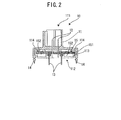
- FIG. 2 is a sectional view taken along the line X-X in FIG. 1 .
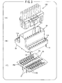
- FIG. 3 is an exploded perspective view of the connector illustrated in FIG. 1 .
- part (A) of FIG. 3 illustrates a mating connector to mate the connector whose external appearance is illustrated in FIG. 1
- perspective views of the connector of the first embodiment are illustrated in parts (B) and (C) of FIG. 3 .
- a connector 10 of the first embodiment includes a housing 11, plural first contacts 12 which are arranged in two rows and plural second contacts 13 which are similarly arranged in two rows.
- the housing 11 includes a mating section 111 and a mount section 112.
- the mating section 111 is an element of the housing 11 which mates with a mating connector 100 (see part (A) of FIG. 3 ).
- the first contacts 12 are provided in the mating section 111, and make contact with contacts (not illustrated) of the mating connector 100 when being mated with the mating connector 100.
- the mount section 112 is an element serving for mounting the housing 11 to a circuit board (not illustrated).
- the second contacts 13 are provided in the mount section 112.
- the second contacts 13 are passed through holes which are provided in the circuit board to penetrate from a top surface to a bottom surface, and the second contacts 13 are soldered to the circuit board on a side of the bottom surface.
- the mount section 112 is provided with solder pegs 14. The solder pegs 14 are passed through holes of the circuit board to be soldered so that the connector 10 is positioned and fixed to the circuit board.
- a circuit arrangement space 113 is formed on a side facing the circuit board in the housing 11.
- An internal circuit 15 illustrated in part (C) of FIG. 3 is arranged so as to face the circuit board in the circuit arrangement space 113.
- the circuit arrangement space 113 is formed in a shape such that the housing 11 forming the circuit arrangement space 113 cover the internal circuit 15 in combination with the circuit board on which the connector 10 is to be mounted.
- a side on the mount section 112 (a bottom side) of the circuit arrangement space 113 is closed by a part of the housing such as a lid included in the housing, to cover the internal circuit 15 arranged in the circuit arrangement space 113 without depending on the circuit board.
- the internal circuit 15 arranged in the circuit arrangement space 113 is a MID (Molded Interconnect Device).
- the internal circuit 15 is a circuit component on which terminals, wiring patterns, electrical components and the like are mounted on a resin molded body.
- Photocouplers 152 and other electronic components are mounted on a resin molded body 151 in the internal circuit 15.
- the first contacts 12 and the second contacts 13 each are connected to the resin molded body 151.
- the first contacts 12 and the second contacts 13 are connected directly or via other electronic components to the photocouplers 152 mounted on the resin molded body 151.
- the photocouplers 152 are circuit elements to electrically insulate the first contacts 12 and the second contacts 13 from each other and relay signals in an optical manner.
- the photocouplers 152 are provided one for each pair of the first contacts 12 and the second contacts 13.
- ventilation openings 114 which communicate the circuit arrangement space 113 in which the internal circuit is arranged with the outside is formed in the housing 11.
- the ventilation openings 114 are ventilation holes to allow heat generated by the electronic components such as the photocouplers 152 included in the internal circuit 15 provided in the circuit arrangement space 113 to dissipate to the outside.
- the ventilation openings 114 are formed such that heat in the circuit arrangement space 113 is allowed to dissipate in a direction in which the heat is cleared from the circuit board in a position in which the connector 10 is mounted on the circuit board.
- the connector 10 is to be mounted on a surface facing upward of the circuit board arranged horizontally while the mating section 111 being facing upward, and the ventilation openings 114 include the configuration to allow heat in the circuit arrangement space 113 to dissipate upwardly.
- the connector 10 of the first embodiment is a connector having a configuration in which the connector 10 itself includes the photocouplers 152, and transmits signals while providing insulation between the first contacts 12 and the second contacts 13. For this reason, according to the connector 10 of the first embodiment, the electrical insulation is provided between the circuit board and the outside. In addition, when the connector 10 of the first embodiment is used, since photocoulers are not required to be mounted on the circuit board, it is possible to allow an area of the circuit board available of wide and effective use.
- ventilation openings 114 are formed in the housing 11 of the connector 10 as the first embodiment, it is avoided that heat accumulates in the circuit arrangement space 113 and thus it is prevented that signal transmission accuracy is deteriorated or the components are degraded due to the photocouplers 152 and the like.
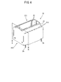
- FIG. 4 is a perspective view illustrating an external appearance of a connector as a second embodiment according to the present invention.
- FIG. 5 is a perspective view of the connector as sectioned along the line X-X illustrated in FIG. 4 .
- FIG. 6 is a sectional view taken along the line X-X illustrated in FIG. 4 .
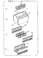
- FIG. 7 is an exploded perspective view of the connector of the second embodiment.
- FIG. 8 is a perspective view of internal circuits included in the connector of the second embodiment.
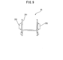
- FIG. 9 is a side view of the internal circuits included in the connector of the second embodiment.
- a connector 20 of the second embodiment includes a housing 21, plural first contacts 22 which are arranged in two rows and plural second contacts 23 which are similarly arranged in two rows.
- the housing 21 includes a mating section 211 and a mount section 212.
- the mating section 211 has a shape same as that of the mating section 111 of the first embodiment, and is an element to mate with the mating connector 100 having the shape illustrated in part (A) of FIG. 3 .
- the first contacts 22 are provided in the mating section 211, and make contact with contacts of the mating connector 100 when being mated with the mating connector 100.
- the mount section 212 is an element serving for mounting the housing 11 to a circuit board (not illustrated).
- the second contacts 23 are provided in the mount section 212, and are passed through holes which are provided in the circuit board, and are soldered to the circuit board on a side of a bottom surface thereof.
- the mount section 212 is provided with solder pegs 24. The solder pegs 24 are passed through holes of the circuit board to be soldered so that the connector 20 is fixed to the circuit board.
- a circuit arrangement space 213 is formed on a side of the mount section 212 facing the circuit board in the housing 21, and an internal circuit 25 having a shape illustrated in FIGS. 8 and 9 is arranged in the circuit arrangement space 213.
- the circuit arrangement space 213 in which the internal circuit 25 is arranged has a configuration in which the housing 21 cover the internal circuit 25 in combination with the circuit board on which the connector 20 is mounted.
- such a configuration may be used that the internal circuit 25 arranged in the circuit arrangement space 213 is covered without depending on the circuit board.
- the internal circuit 25 arranged in the circuit arrangement space 213 is an MID, and as illustrate in FIG. 9 , the photocouplers 252 and other electronic components are mounted on side surfaces of a resin molded body 251 having a sectional shape of H.
- the side surfaces on which the photocouplers 252 and the like are mounted of the resin molded body 251 are surfaces which spread in a direction standing up with respect to the circuit board when the connector 20 is mounted on the circuit board.
- the second contacts 23 are passed through the resin molded body 251 to be fixed to the resin molded body 251, and in addition, the first contacts 22 are also passed through to be fixed to the resin molded body 251.
- the photocouplers 252 and other electronic components are provided one for each pair of the first contacts 22 and the second contacts 23.
- the first contacts 22 and the second contacts 23 are connected directly or via other electronic components to the respective photocouplers 252.
- the photocouplers 252 are circuit elements to electrically insulate the first contacts 22 and the second contacts 23 from each other and optically relay signals.
- ventilation openings 214 open to the circuit arrangement space 213 in which the internal circuit 25 is arranged, and penetrate in an upward direction away from the circuit board.
- the ventilation openings 214 are ones to allow heat generated by the photocouplers 252 and the like in the internal circuit 25 to dissipate.
- the connector 20 of the second embodiment is a connector having a configuration in which the connector 20 itself includes the photocouplers 252, and transmits signals while providing electrical insulation between the first contacts 22 and the second contacts 23.
- the connector 20 of the second embodiment since the photocouplers are not required to be mounted on the circuit board, it is possible to allow an area of the circuit board to be available for wide and effective use.
- the connector 20 of the second embodiment includes the photocouplers 252 mounted on the side surface spreading in the direction standing up with respect to the circuit board. For this reason, a projected area thereof on the circuit board is reduced and thus it is possible to allow the area of the circuit board to be available further more for a wide and effective use.
- FIG. 10 is a perspective view of a connector as a third embodiment.
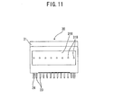
- FIG. 11 is a side view of the connector as the third embodiment.
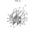
- FIG. 12 is a perspective view as sectioned along the line X-X in FIG. 10 .
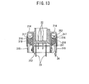
- FIG. 13 is a sectional view taken along the line X-X in FIG. 10 .
- a connector 30 of the third embodiment is different only in a housing 31.
- elements except for the housing 31 are denoted using the same reference signs as those used for the connector 20 of the second embodiment.
- housing 31 also, elements same as those of the above-described housing 21 of the second embodiment are denoted using the same reference signs as those used for the housing 21 of the second embodiment, and in the following, differences of the housing 31 from the housing 21 of the second embodiment will be described.
- the housing 31 of the connector 30 is provided with partition walls 315 on both side surfaces thereof.
- the partition walls 315 form partial areas of inner wall surfaces defining the circuit arrangement space 213 in which the internal circuit 25 is arranged, and partial areas of outer surfaces defining an external appearance of the connector 30.
- the partition walls 315 themselves are included also in the above-described housing 21 of the second embodiment, and however, each of the partition walls 315 of the housing 31 in the third embodiment is further formed with metal layers 316, 317 for heat dissipation on an inner wall surface and an outer wall surface each thereof.
- the metal layers 317 spread on areas facing the photocouplers included in the internal circuit 25.
- the metal layers 316, 317 formed on the inner wall surface and the outer wall surface are connected with each other by metal embedded in openings 318 passing through from the inner wall surfaces to the outer wall surfaces, reepectively.
- the metal layers and the like are formed by the above-described MID.
- These metal layers 316, 317 are for conducting heat in the circuit arrangement space 213 from the metal layers 316 on the inner surface sides via the metal embedded in the openings 318 of the partition walls 315 to the metal layers 317 on the outer surface sides to dissipate the heat.
- the third embodiment is also provided with the ventilation openings 214 for heat dissipation, and heat in the circuit arrangement space 213 is dissipated by two ways of the ventilation openings 214 and the metal layers 316, 317.
- the heat in the circuit arrangement space 213 is dissipated more effectively.
- FIG. 14 is a perspective view of a connector as a fourth embodiment.
- FIG. 15 is a sectional view taken along the line X-X in FIG. 14 .
- FIG. 16 is a perspective view of a housing of the fourth embodiment.
- FIG. 17 is a sectional view taken along the line X-X in FIG. 16 .
- a connector 40 of the fourth embodiment is different only in a part of elements of a housing 41. For this reason, elements except for the different elements are denoted using the same reference signs as those used for the connector 20 of the second embodiment, and only differences from the
- the housing 41 of the fourth embodiment is also provided with partition walls 415 on both side surfaces thereof.
- the partition walls 415 form partial areas of inner wall surfaces defining the circuit arrangement space 213 in which the internal circuit 25 is arranged, and partial areas of outer surfaces defining an external appearance of the connector 40.
- the housing 41 of the fourth embodiment is a two-color mold of a first resin having insulation and low thermal conductivity and a second resin having electrical conductivity and high thermal conductivity.
- the first resin has a thermal conductivity which is lower than the thermal conductivity of the second resin.
- the partition walls 415 are formed using the second resin which has the high thermal conductivity. A portion formed by using the second resin may be spread further from the partition walls 415 as far as the portion is not included in a part requiring insulation such a part that holds the first contacts 21 or the second contacts 22.
- the partition walls 415 are formed using the second resin having the high thermal conductivity, heat in the circuit arrangement space 213 is dissipated via the ventilation openings 214, and also via the partition walls 415. For this reason, the heat in the circuit arrangement space 213 is dissipated further effectively.
Abstract
Description
- The present invention relates to a connector to be mounted on a circuit board and mate with a mating connector.
- There has been known a connector which is mounted on a circuit board and mates with a mating connector to connect between the mating connector outside the circuit board and an electronic circuit on the circuit board. Among such circuit boards having connectors being mounted thereon, there is one configured to once receive with a photocoupler (opto-isolator) an electric signal transmitted via a connector to a circuit board to insulate the electronic signal and transmit with the photocoupler the signal electrically insulated from the outside to a next circuit on the circuit board. By applying this configuration, possibilities of malfunctions or failures in an electronic circuit on the circuit board by noise from the outside are reduced because of being electrically isolated from the outside by the photocoupler. In addition, the electronic circuit on the circuit board may be operated with a power supply voltage different from that of the outside. However, in such configuration, the photocoupler, which does not dirctly contribute signal processing, is required to be mounted on the circuit board. For this reason, specifically in a configuration in which the number of signal lines is large, photocouplers whose count is consistent with the number of signal lines are arranged on the circuit board and thus a wide area is required on the circuit board. In such a case, an area for arrangement of electronic components serving for substantial signal processing is constrained.
- Japanese Patent Publication
JP 2005-191139A JP 2005-268009A - In view of the foregoing, the present invention has been made to provide a connector which effectively allows an area on a circuit board available of wide and effective use for signal processing, when it is required to provide electrical insulation between an electronic circuit on the circuit board and the outside.
- A connector according to the present invention includes: a housing that includes a mating section which includes a first contact to make contact with a contact of a mating connector when mating with the mating connector, and a mount section which includes a second contact to be connected to a circuit board when mounted on the circuit board and is mounted on the circuit board; and an electronic circuit that is connected to both of the first contact and the second contact directly or via another circuit device, and includes a photocoupler which electrically insulates the first contact and the second contact from each other and relays a signal in an optical manner. Alternatively, the connector according to the invention includes an electronic circuit, the electronic circuit being connected to both of a first contact and a second contact directly or via another circuit device, and the electronic circuit also including a photocoupler which electrically insulates the first contact and the second contact from each other and relays a signal in an optical manner.
- The connector according to the present invention is configured to include in itself the photocoupler which transmits a signal while providing electrical insulation between the first contact and the second contact. For this reason, thanks to the connector, the electrical insulation is provided between the circuit on the circuit board and the outside. In addition, according to the connector of the present invention, it is possible to allow an area of the circuit board available for a wide and effective use, compared to a case in which a photocoupler is arranged on a circuit board.
- Here, in the connector according to the present invention, it is preferable that the housing has a shape to cover the electronic circuit independently or together with the circuit board in a state in which the housing is mounted on the circuit board, and includes a ventilation opening for heat radiation to release heat generated by the electronic circuit in a direction away from the circuit board in the state in which the housing is mounted on the circuit board.
- The ventilation opening is provided, and it is prevented that heat accumulates in the connector, and thus, it is possible to allow the photocoupler and other electronic components included in the connector to operate further stably.
- In addition, in the connector according to the present invention, it is preferable that the housing includes a partition wall which forms both a partial area of an inner wall surface defining a space in which the electronic circuit is provided and a partial area of an outer wall surface defining an outer shape of the connector, and includes metal layers for heat radiation connected with each other by using metal which metal layers are on each of the inner wall surface and the outer wall surface, respectively.
- Also, since such metal layers for heat radiation are provided, it is prevented that heat accumulates in the connector, and it is possible to allow still further stable operations.
- Furthermore, in the connector according to the present invention, it is preferable that the housing includes a partition wall which forms both a partial area of an inner wall surface defining a space in which the electronic circuit is provided and a partial area of an outer wall surface defining an outer shape of the connector, and the housing is a two-color mold by first resin whose thermal conductivity is relatively low and second resin whose thermal conductivity is relatively high, and the partition wall is formed by the second resin.
- The housing serves for holding the contacts while providing insulation between adjacent contacts and thus the housing is required to be an insulating element. However, insulating elements generally have low thermal conductivity. For this reason, as described above, the housing is formed by two-color molding, and the first resin having high insulation is used for a portion in which insulation is to be secured and the second resin which has high thermal conductivity while having low insulation is used for the above-described partition wall, and thereby, it is prevented that heat accumulates inside while having functions of a housing.
- Here, in the connector according to the present invention, it is preferable that the photocoupler is mounted on a mount surface spreading in a direction standing up with respect to the circuit board in the state in which the connector is mounted on the circuit board.
- The photocoupler is mounted on the mount surface spreading in the direction standing up with respect to the circuit board, and thus, it is possible to reduce a projected area thereof on the circuit board and thus it is possible to allow the area of the circuit board available furthermore for a wide and effective use.
- As described above, according to the connector of the invention, it is possible to transmit electrical signals while providing insulation between an electronic component on a circuit board and the outside, and to make effective use of the circuit board.
- BRIEF DESCRIPTION OF THE DRAWINGS
-
FIG. 1 is a perspective view illustrating a external appearance of a connector as an embodiment according to the present invention; -
FIG. 2 is a sectional view taken along the line X-X inFIG. 1 ; -
FIG. 3 is an exploded perspective view of the connector illustrated inFIG. 1 ; -
FIG. 4 is a perspective view illustrating an external appearance of a connector as a second embodiment according to the present invention; -
FIG. 5 is a perspective view of the connector as sectioned along the line X-X illustrated inFIG. 4 ; -
FIG. 6 is a sectional view taken along the line X-X illustrated inFIG. 4 ; -
FIG. 7 is an exploded perspective view of the connector as the second embodiment; -
FIG. 8 is a perspective view of internal circuits included in the connector of the second embodiment; -
FIG. 9 is a side view of the internal circuits included in the connector of the second embodiment; -
FIG. 10 is a perspective view of a connector as a third embodiment; -
FIG. 11 is a side view of the connector as the third embodiment; -
FIG. 12 is a perspective view as sectioned along the line X-X inFIG. 10 ; -
FIG. 13 is a sectional view taken along the line X-X inFIG. 10 ; -
FIG. 14 is a perspective view of a connector as a fourth embodiment; -
FIG. 15 is a sectional view taken along the line X-X inFIG. 14 . -
FIG. 16 is a perspective view of a housing as the fourth embodiment; and -
FIG. 17 is a sectional view taken along the line X-X inFIG. 16 . - Embodiments of the connector of the present invention will be described in the followings.
-
FIG. 1 is a perspective view illustrating an external appearance of a connector as an embodiment according to the present invention. In addition,FIG. 2 is a sectional view taken along the line X-X inFIG. 1 . Further,FIG. 3 is an exploded perspective view of the connector illustrated inFIG. 1 . However, part (A) ofFIG. 3 illustrates a mating connector to mate the connector whose external appearance is illustrated inFIG. 1 , and perspective views of the connector of the first embodiment are illustrated in parts (B) and (C) ofFIG. 3 . - A
connector 10 of the first embodiment includes ahousing 11, pluralfirst contacts 12 which are arranged in two rows and pluralsecond contacts 13 which are similarly arranged in two rows. - The
housing 11 includes amating section 111 and amount section 112. Themating section 111 is an element of thehousing 11 which mates with a mating connector 100 (see part (A) ofFIG. 3 ). Thefirst contacts 12 are provided in themating section 111, and make contact with contacts (not illustrated) of themating connector 100 when being mated with themating connector 100. In addition, themount section 112 is an element serving for mounting thehousing 11 to a circuit board (not illustrated). Thesecond contacts 13 are provided in themount section 112. Thesecond contacts 13 are passed through holes which are provided in the circuit board to penetrate from a top surface to a bottom surface, and thesecond contacts 13 are soldered to the circuit board on a side of the bottom surface. In addition, themount section 112 is provided withsolder pegs 14. Thesolder pegs 14 are passed through holes of the circuit board to be soldered so that theconnector 10 is positioned and fixed to the circuit board. - In addition, as illustrated in
FIG. 2 , acircuit arrangement space 113 is formed on a side facing the circuit board in thehousing 11. Aninternal circuit 15 illustrated in part (C) ofFIG. 3 is arranged so as to face the circuit board in thecircuit arrangement space 113. Thecircuit arrangement space 113 is formed in a shape such that thehousing 11 forming thecircuit arrangement space 113 cover theinternal circuit 15 in combination with the circuit board on which theconnector 10 is to be mounted. Incidentally, such a configuration may be used that a side on the mount section 112 (a bottom side) of thecircuit arrangement space 113 is closed by a part of the housing such as a lid included in the housing, to cover theinternal circuit 15 arranged in thecircuit arrangement space 113 without depending on the circuit board. - The
internal circuit 15 arranged in thecircuit arrangement space 113 is a MID (Molded Interconnect Device). In other words, theinternal circuit 15 is a circuit component on which terminals, wiring patterns, electrical components and the like are mounted on a resin molded body.Photocouplers 152 and other electronic components are mounted on a resin moldedbody 151 in theinternal circuit 15. Thefirst contacts 12 and thesecond contacts 13 each are connected to the resin moldedbody 151. Thefirst contacts 12 and thesecond contacts 13 are connected directly or via other electronic components to thephotocouplers 152 mounted on the resin moldedbody 151. Thephotocouplers 152 are circuit elements to electrically insulate thefirst contacts 12 and thesecond contacts 13 from each other and relay signals in an optical manner. Thephotocouplers 152 are provided one for each pair of thefirst contacts 12 and thesecond contacts 13. - In addition,
ventilation openings 114 which communicate thecircuit arrangement space 113 in which the internal circuit is arranged with the outside is formed in thehousing 11. Theventilation openings 114 are ventilation holes to allow heat generated by the electronic components such as thephotocouplers 152 included in theinternal circuit 15 provided in thecircuit arrangement space 113 to dissipate to the outside. - The
ventilation openings 114 are formed such that heat in thecircuit arrangement space 113 is allowed to dissipate in a direction in which the heat is cleared from the circuit board in a position in which theconnector 10 is mounted on the circuit board. Theconnector 10 is to be mounted on a surface facing upward of the circuit board arranged horizontally while themating section 111 being facing upward, and theventilation openings 114 include the configuration to allow heat in thecircuit arrangement space 113 to dissipate upwardly. - As described above, the
connector 10 of the first embodiment is a connector having a configuration in which theconnector 10 itself includes thephotocouplers 152, and transmits signals while providing insulation between thefirst contacts 12 and thesecond contacts 13. For this reason, according to theconnector 10 of the first embodiment, the electrical insulation is provided between the circuit board and the outside. In addition, when theconnector 10 of the first embodiment is used, since photocoulers are not required to be mounted on the circuit board, it is possible to allow an area of the circuit board available of wide and effective use. - In addition, since the above-described
ventilation openings 114 are formed in thehousing 11 of theconnector 10 as the first embodiment, it is avoided that heat accumulates in thecircuit arrangement space 113 and thus it is prevented that signal transmission accuracy is deteriorated or the components are degraded due to thephotocouplers 152 and the like. -
FIG. 4 is a perspective view illustrating an external appearance of a connector as a second embodiment according to the present invention.FIG. 5 is a perspective view of the connector as sectioned along the line X-X illustrated inFIG. 4 .FIG. 6 is a sectional view taken along the line X-X illustrated inFIG. 4 .FIG. 7 is an exploded perspective view of the connector of the second embodiment.FIG. 8 is a perspective view of internal circuits included in the connector of the second embodiment.FIG. 9 is a side view of the internal circuits included in the connector of the second embodiment. - Similar to the above-described
connector 10 of the first embodiment, aconnector 20 of the second embodiment includes ahousing 21, pluralfirst contacts 22 which are arranged in two rows and pluralsecond contacts 23 which are similarly arranged in two rows. - The
housing 21 includes amating section 211 and amount section 212. Themating section 211 has a shape same as that of themating section 111 of the first embodiment, and is an element to mate with themating connector 100 having the shape illustrated in part (A) ofFIG. 3 . - The
first contacts 22 are provided in themating section 211, and make contact with contacts of themating connector 100 when being mated with themating connector 100. - In addition, the
mount section 212 is an element serving for mounting thehousing 11 to a circuit board (not illustrated). Thesecond contacts 23 are provided in themount section 212, and are passed through holes which are provided in the circuit board, and are soldered to the circuit board on a side of a bottom surface thereof. In addition, also similar to theconnector 10 of the first embodiment, themount section 212 is provided with solder pegs 24. The solder pegs 24 are passed through holes of the circuit board to be soldered so that theconnector 20 is fixed to the circuit board. - In addition, a
circuit arrangement space 213 is formed on a side of themount section 212 facing the circuit board in thehousing 21, and aninternal circuit 25 having a shape illustrated inFIGS. 8 and9 is arranged in thecircuit arrangement space 213. Thecircuit arrangement space 213 in which theinternal circuit 25 is arranged has a configuration in which thehousing 21 cover theinternal circuit 25 in combination with the circuit board on which theconnector 20 is mounted. However, also similar to the description of the above-described first embodiment, such a configuration may be used that theinternal circuit 25 arranged in thecircuit arrangement space 213 is covered without depending on the circuit board. - The
internal circuit 25 arranged in thecircuit arrangement space 213 is an MID, and as illustrate inFIG. 9 , thephotocouplers 252 and other electronic components are mounted on side surfaces of a resin moldedbody 251 having a sectional shape of H. The side surfaces on which thephotocouplers 252 and the like are mounted of the resin moldedbody 251 are surfaces which spread in a direction standing up with respect to the circuit board when theconnector 20 is mounted on the circuit board. - The
second contacts 23 are passed through the resin moldedbody 251 to be fixed to the resin moldedbody 251, and in addition, thefirst contacts 22 are also passed through to be fixed to the resin moldedbody 251. Thephotocouplers 252 and other electronic components are provided one for each pair of thefirst contacts 22 and thesecond contacts 23. Thefirst contacts 22 and thesecond contacts 23 are connected directly or via other electronic components to therespective photocouplers 252. Thephotocouplers 252 are circuit elements to electrically insulate thefirst contacts 22 and thesecond contacts 23 from each other and optically relay signals. - In addition,
ventilation openings 214 open to thecircuit arrangement space 213 in which theinternal circuit 25 is arranged, and penetrate in an upward direction away from the circuit board. Theventilation openings 214 are ones to allow heat generated by thephotocouplers 252 and the like in theinternal circuit 25 to dissipate. - Similar to the above-described
connector 10 of the first embodiment, theconnector 20 of the second embodiment is a connector having a configuration in which theconnector 20 itself includes thephotocouplers 252, and transmits signals while providing electrical insulation between thefirst contacts 22 and thesecond contacts 23. Thus, according to theconnector 20 of the second embodiment, since the photocouplers are not required to be mounted on the circuit board, it is possible to allow an area of the circuit board to be available for wide and effective use. - In addition, as different things from those of the
connector 10 of the first embodiment, theconnector 20 of the second embodiment includes thephotocouplers 252 mounted on the side surface spreading in the direction standing up with respect to the circuit board. For this reason, a projected area thereof on the circuit board is reduced and thus it is possible to allow the area of the circuit board to be available further more for a wide and effective use. - In addition, similar to the
connector 10 of the first embodiment for this aspect, since theventilation openings 214 are formed in thehousing 21 of theconnector 20, it is avoided that heat accumulates in thecircuit arrangement space 213 and thus it is prevented that signal transmission accuracy is deteriorated or components are degraded with respect to thephotocouplers 252 and the like. -
FIG. 10 is a perspective view of a connector as a third embodiment. In addition,FIG. 11 is a side view of the connector as the third embodiment. Further,FIG. 12 is a perspective view as sectioned along the line X-X inFIG. 10 .FIG. 13 is a sectional view taken along the line X-X inFIG. 10 . - Comparing to the above-described
connector 20 of the second embodiment, aconnector 30 of the third embodiment is different only in ahousing 31. For this reason, elements except for thehousing 31 are denoted using the same reference signs as those used for theconnector 20 of the second embodiment. - In addition, for the
housing 31 also, elements same as those of the above-describedhousing 21 of the second embodiment are denoted using the same reference signs as those used for thehousing 21 of the second embodiment, and in the following, differences of thehousing 31 from thehousing 21 of the second embodiment will be described. - The
housing 31 of theconnector 30 is provided withpartition walls 315 on both side surfaces thereof. Thepartition walls 315 form partial areas of inner wall surfaces defining thecircuit arrangement space 213 in which theinternal circuit 25 is arranged, and partial areas of outer surfaces defining an external appearance of theconnector 30. Thepartition walls 315 themselves are included also in the above-describedhousing 21 of the second embodiment, and however, each of thepartition walls 315 of thehousing 31 in the third embodiment is further formed withmetal layers internal circuit 25. In addition, the metal layers 316, 317 formed on the inner wall surface and the outer wall surface are connected with each other by metal embedded inopenings 318 passing through from the inner wall surfaces to the outer wall surfaces, reepectively. The metal layers and the like are formed by the above-described MID. These metal layers 316, 317 are for conducting heat in thecircuit arrangement space 213 from the metal layers 316 on the inner surface sides via the metal embedded in theopenings 318 of thepartition walls 315 to the metal layers 317 on the outer surface sides to dissipate the heat. - Similar to the above-described second embodiment, the third embodiment is also provided with the
ventilation openings 214 for heat dissipation, and heat in thecircuit arrangement space 213 is dissipated by two ways of theventilation openings 214 and the metal layers 316, 317. Thus, the heat in thecircuit arrangement space 213 is dissipated more effectively. -
FIG. 14 is a perspective view of a connector as a fourth embodiment. In addition,FIG. 15 is a sectional view taken along the line X-X inFIG. 14 . Further,FIG. 16 is a perspective view of a housing of the fourth embodiment.FIG. 17 is a sectional view taken along the line X-X inFIG. 16 . - Comparing to the above-described
connector 20 of the second embodiment, aconnector 40 of the fourth embodiment is different only in a part of elements of ahousing 41. For this reason, elements except for the different elements are denoted using the same reference signs as those used for theconnector 20 of the second embodiment, and only differences from the - The
housing 41 of the fourth embodiment is also provided withpartition walls 415 on both side surfaces thereof. Thepartition walls 415 form partial areas of inner wall surfaces defining thecircuit arrangement space 213 in which theinternal circuit 25 is arranged, and partial areas of outer surfaces defining an external appearance of theconnector 40. - The
housing 41 of the fourth embodiment is a two-color mold of a first resin having insulation and low thermal conductivity and a second resin having electrical conductivity and high thermal conductivity. The first resin has a thermal conductivity which is lower than the thermal conductivity of the second resin. Thepartition walls 415 are formed using the second resin which has the high thermal conductivity. A portion formed by using the second resin may be spread further from thepartition walls 415 as far as the portion is not included in a part requiring insulation such a part that holds thefirst contacts 21 or thesecond contacts 22. - In the present embodiment, since the
partition walls 415 are formed using the second resin having the high thermal conductivity, heat in thecircuit arrangement space 213 is dissipated via theventilation openings 214, and also via thepartition walls 415. For this reason, the heat in thecircuit arrangement space 213 is dissipated further effectively.
Claims (9)
- A connector (20) comprising:a housing (21) that includes a mating section (211) which includes a first contact (22) to make contact with a contact of a mating connector (100) when mating with the mating connector (100), and a mount section (212) which includes a second contact (23) to be connected to a circuit board when the mount section (212) is mounted on the circuit board; andan electronic circuit (25) that is connected to both of the first contact (22) and the second contact (23), and includes a photocoupler (252) which electrically insulates the first contact (22) and the second contact (23) from each other and relays a signal in an optical manner.
- The connector according to claim 1, wherein the electronic circuit (25) is directly connected to both of the first contact (22) and the second contact (23).
- The connector according to claim 1, wherein the electronic circuit (25) is connected to both of the first contact (22) and the second contact (23) via another circuit device.
- The connector according to claim 1, 2 or 3, wherein the housing (21) has a shape to cover the electronic circuit (25), and includes a ventilation opening (214) for heat radiation to release heat generated by the electronic circuit (25) in a direction away from the circuit board in the state in which the housing (21) is mounted on the circuit board.
- The connector according to claim 4, wherein the shape of the housing (21) is arranged to cover the electronic circuit (25) independently.
- The connector according to claim 4, wherein the shape of the housing (21) is arranged to cover the electronic circuit (25) together with the circuit board in a state in which the housing (21) is mounted on the circuit board.
- The connector according to any preceding claim, wherein the housing (31) includes a partition wall (315) which forms both a partial area of an inner wall surface defining a space (213) in which the electronic circuit (25) is provided and a partial area of an outer wall surface defining an outer shape of the connector (30), and includes metal layers (316, 317) for heat radiation connected with each other by using metal which metal layers (316, 317) are on each of the inner wall surface and the outer wall surface, respectively.
- The connector according to any one of claims 1 to 6, wherein
the housing (41) includes a partition wall (415) which forms both a partial area of an inner wall surface defining a space (213) in which the electronic circuit (25) is provided and a partial area of an outer wall surface defining an outer shape of the connector (40),
the housing (41) is a two-color mold comprising a first resin whose thermal conductivity is relatively low and a second resin whose thermal conductivity is relatively high, and
the partition wall (415) is formed by the second resin. - The connector according to any preceding claim, wherein the photocoupler (252) is mounted on a mount surface spreading in a direction standing up with respect to the circuit board in the state in which the connector (20) is mounted on the circuit board.
Applications Claiming Priority (1)
| Application Number | Priority Date | Filing Date | Title |
|---|---|---|---|
| JP2012164652A JP5872405B2 (en) | 2012-07-25 | 2012-07-25 | connector |
Publications (1)
| Publication Number | Publication Date |
|---|---|
| EP2690722A1 true EP2690722A1 (en) | 2014-01-29 |
Family
ID=48832827
Family Applications (1)
| Application Number | Title | Priority Date | Filing Date |
|---|---|---|---|
| EP13177907.6A Withdrawn EP2690722A1 (en) | 2012-07-25 | 2013-07-24 | Connector |
Country Status (5)
| Country | Link |
|---|---|
| US (1) | US20140027656A1 (en) |
| EP (1) | EP2690722A1 (en) |
| JP (1) | JP5872405B2 (en) |
| KR (1) | KR20140013947A (en) |
| CN (1) | CN103579864A (en) |
Families Citing this family (3)
| Publication number | Priority date | Publication date | Assignee | Title |
|---|---|---|---|---|
| WO2018227575A1 (en) * | 2017-06-16 | 2018-12-20 | 深圳市得城网络科技有限公司 | Portable repeater |
| US11525709B2 (en) * | 2019-04-11 | 2022-12-13 | Veoneer Us, Llc | Electronic unit with vent integrated with terminal aperture |
| JP7140076B2 (en) | 2019-08-30 | 2022-09-21 | 株式会社オートネットワーク技術研究所 | connector |
Citations (9)
| Publication number | Priority date | Publication date | Assignee | Title |
|---|---|---|---|---|
| US4082407A (en) * | 1977-05-20 | 1978-04-04 | Amerace Corporation | Terminal block with encapsulated heat sink |
| US20030012363A1 (en) * | 2001-07-16 | 2003-01-16 | Loeb Frederick F. | Jack module with integrated modem interface circuits |
| JP2005191139A (en) | 2003-12-24 | 2005-07-14 | Kyocera Corp | Multiple-pattern wiring board |
| WO2005065254A2 (en) * | 2003-12-31 | 2005-07-21 | Fci Americas Technology, Inc. | Electrical power contacts and connectors comprising same |
| JP2005268009A (en) | 2004-03-18 | 2005-09-29 | Auto Network Gijutsu Kenkyusho:Kk | Connector device with controlling function |
| US20080096429A1 (en) * | 2006-10-19 | 2008-04-24 | Tyco Electronics Corporation | Subminiature electrical connector including over-voltage and over-current circuit protection |
| US20100136806A1 (en) * | 2008-12-03 | 2010-06-03 | Advanced Connectek Inc. | Insulative housing and electrical connector with an insulative housing |
| US20100273347A1 (en) * | 2009-04-24 | 2010-10-28 | Alltop Electronics (Suzhou) Co., Ltd. | Electrical connector and electrical connector assembly having heat-radiating structure |
| WO2012019068A2 (en) * | 2010-08-06 | 2012-02-09 | Fci | Electrical connector assembly including compliant heat sink |
Family Cites Families (12)
| Publication number | Priority date | Publication date | Assignee | Title |
|---|---|---|---|---|
| JPS57153306A (en) * | 1981-03-17 | 1982-09-21 | Matsushita Electric Works Ltd | Sequence controller |
| JPH0192784U (en) * | 1987-12-11 | 1989-06-19 | ||
| JPH0319276U (en) * | 1989-07-04 | 1991-02-26 | ||
| JPH08130077A (en) * | 1994-10-31 | 1996-05-21 | Matsushita Electric Works Ltd | Lamp socket |
| US6533470B2 (en) * | 2001-03-16 | 2003-03-18 | Infineon Technologies North America Corp. | Single-piece cage for pluggable fiber optic transceiver |
| US20030235375A1 (en) * | 2002-06-25 | 2003-12-25 | Kamath Kishore K. | Transceivers with improved cross talk |
| JP4360859B2 (en) * | 2003-05-29 | 2009-11-11 | 株式会社日立製作所 | Electronics |
| CN101174745B (en) * | 2006-10-19 | 2012-07-04 | 泰科电子公司 | Subminiature electrical connector including over-voltage and over-current circuit protection |
| KR100972979B1 (en) * | 2008-03-17 | 2010-07-29 | 삼성엘이디 주식회사 | Led package and manufacturing method for the same |
| CN102714495B (en) * | 2010-01-19 | 2014-12-17 | 江森自控科技公司 | Optocoupler circuit for gate driver |
| JP2011249285A (en) * | 2010-05-31 | 2011-12-08 | Yazaki Corp | Led unit |
| US9279946B2 (en) * | 2012-05-23 | 2016-03-08 | Avago Technologies General Ip (Singapore) Pte. Ltd. | Premolded cavity for optoelectronic device |
-
2012
- 2012-07-25 JP JP2012164652A patent/JP5872405B2/en not_active Expired - Fee Related
-
2013
- 2013-07-18 KR KR1020130084730A patent/KR20140013947A/en not_active Application Discontinuation
- 2013-07-24 EP EP13177907.6A patent/EP2690722A1/en not_active Withdrawn
- 2013-07-24 US US13/949,716 patent/US20140027656A1/en not_active Abandoned
- 2013-07-25 CN CN201310315067.XA patent/CN103579864A/en active Pending
Patent Citations (9)
| Publication number | Priority date | Publication date | Assignee | Title |
|---|---|---|---|---|
| US4082407A (en) * | 1977-05-20 | 1978-04-04 | Amerace Corporation | Terminal block with encapsulated heat sink |
| US20030012363A1 (en) * | 2001-07-16 | 2003-01-16 | Loeb Frederick F. | Jack module with integrated modem interface circuits |
| JP2005191139A (en) | 2003-12-24 | 2005-07-14 | Kyocera Corp | Multiple-pattern wiring board |
| WO2005065254A2 (en) * | 2003-12-31 | 2005-07-21 | Fci Americas Technology, Inc. | Electrical power contacts and connectors comprising same |
| JP2005268009A (en) | 2004-03-18 | 2005-09-29 | Auto Network Gijutsu Kenkyusho:Kk | Connector device with controlling function |
| US20080096429A1 (en) * | 2006-10-19 | 2008-04-24 | Tyco Electronics Corporation | Subminiature electrical connector including over-voltage and over-current circuit protection |
| US20100136806A1 (en) * | 2008-12-03 | 2010-06-03 | Advanced Connectek Inc. | Insulative housing and electrical connector with an insulative housing |
| US20100273347A1 (en) * | 2009-04-24 | 2010-10-28 | Alltop Electronics (Suzhou) Co., Ltd. | Electrical connector and electrical connector assembly having heat-radiating structure |
| WO2012019068A2 (en) * | 2010-08-06 | 2012-02-09 | Fci | Electrical connector assembly including compliant heat sink |
Non-Patent Citations (2)
| Title |
|---|
| "Opto-isolator", 24 May 2012 (2012-05-24), wikipedia, XP055084413, Retrieved from the Internet <URL:http://en.wikipedia.org/wiki/Opto-isolator> [retrieved on 20131018] * |
| MISUMI: "Plastic Molding Tutorial > #127 Special Injection Molding Methods (Two Color Injection Molding Method)", 15 June 2012 (2012-06-15), Misumi Technical Tutorials, XP055084395, Retrieved from the Internet <URL:http://www.misumi-techcentral.com/tt/en/mold/2012/06/127-special-injection-molding-methods-two-color-injection-molding-method.html> [retrieved on 20131018] * |
Also Published As
| Publication number | Publication date |
|---|---|
| CN103579864A (en) | 2014-02-12 |
| JP5872405B2 (en) | 2016-03-01 |
| US20140027656A1 (en) | 2014-01-30 |
| JP2014026766A (en) | 2014-02-06 |
| KR20140013947A (en) | 2014-02-05 |
Similar Documents
| Publication | Publication Date | Title |
|---|---|---|
| US9188752B2 (en) | Optical-electrical connector having inproved heat sink | |
| JP6086407B2 (en) | Electronic control unit | |
| JP7403085B2 (en) | Connectors and connector devices | |
| JP2024026440A (en) | Connector device, connector and mating connector | |
| EP2690722A1 (en) | Connector | |
| US7922509B2 (en) | Surface mount electrical connector having insulated pin | |
| US20150017836A1 (en) | Active plug connector and method for assembling the same | |
| US20100304582A1 (en) | Inverse coplanar electrical connector | |
| US20120196457A1 (en) | Terminal and terminal connecting construction | |
| JP2007325345A (en) | Electrical connection box | |
| KR20190049296A (en) | Electronic control device | |
| KR20170014245A (en) | Receptacle | |
| WO2018038008A1 (en) | Coil assembly, circuit component, and junction box | |
| CN113853075B (en) | Assembly with radiator core forming a load-bearing structure | |
| JP2019119325A (en) | Electric connection device | |
| JP6296875B2 (en) | Electronic component unit | |
| JP5780082B2 (en) | Power box equipment | |
| US20210267070A1 (en) | Electrical connection box | |
| JP5370731B2 (en) | CIRCUIT UNIT, CIRCUIT COMPOSITION, ELECTRIC CONNECTION BOX, AND CIRCUIT UNIT MANUFACTURING METHOD | |
| KR102255501B1 (en) | Receptacle connector and electronic device including the same | |
| JP2007116808A (en) | Board module and electric connection box | |
| JP5545492B2 (en) | Electrical junction box | |
| JP2014203716A (en) | Female connector and card edge connector | |
| TWM537337U (en) | Power connection device and conduction bus member | |
| KR102464355B1 (en) | Connector assembly |
Legal Events
| Date | Code | Title | Description |
|---|---|---|---|
| PUAI | Public reference made under article 153(3) epc to a published international application that has entered the european phase |
Free format text: ORIGINAL CODE: 0009012 |
|
| AK | Designated contracting states |
Kind code of ref document: A1 Designated state(s): AL AT BE BG CH CY CZ DE DK EE ES FI FR GB GR HR HU IE IS IT LI LT LU LV MC MK MT NL NO PL PT RO RS SE SI SK SM TR |
|
| AX | Request for extension of the european patent |
Extension state: BA ME |
|
| 17P | Request for examination filed |
Effective date: 20140715 |
|
| RBV | Designated contracting states (corrected) |
Designated state(s): AL AT BE BG CH CY CZ DE DK EE ES FI FR GB GR HR HU IE IS IT LI LT LU LV MC MK MT NL NO PL PT RO RS SE SI SK SM TR |
|
| 17Q | First examination report despatched |
Effective date: 20160329 |
|
| GRAP | Despatch of communication of intention to grant a patent |
Free format text: ORIGINAL CODE: EPIDOSNIGR1 |
|
| RIC1 | Information provided on ipc code assigned before grant |
Ipc: H01R 13/66 20060101AFI20180306BHEP Ipc: H01R 13/504 20060101ALI20180306BHEP Ipc: H01R 12/58 20110101ALN20180306BHEP Ipc: H01R 12/71 20110101ALI20180306BHEP |
|
| RIC1 | Information provided on ipc code assigned before grant |
Ipc: H01R 13/66 20060101AFI20180313BHEP Ipc: H01R 12/58 20110101ALN20180313BHEP Ipc: H01R 12/71 20110101ALI20180313BHEP Ipc: H01R 13/504 20060101ALI20180313BHEP |
|
| INTG | Intention to grant announced |
Effective date: 20180327 |
|
| STAA | Information on the status of an ep patent application or granted ep patent |
Free format text: STATUS: THE APPLICATION IS DEEMED TO BE WITHDRAWN |
|
| 18D | Application deemed to be withdrawn |
Effective date: 20180807 |