EP2540780A1 - Composition for forming resist underlayer film and patterning process using the same - Google Patents
Composition for forming resist underlayer film and patterning process using the same Download PDFInfo
- Publication number
- EP2540780A1 EP2540780A1 EP20120004626 EP12004626A EP2540780A1 EP 2540780 A1 EP2540780 A1 EP 2540780A1 EP 20120004626 EP20120004626 EP 20120004626 EP 12004626 A EP12004626 A EP 12004626A EP 2540780 A1 EP2540780 A1 EP 2540780A1
- Authority
- EP
- European Patent Office
- Prior art keywords
- silicon
- underlayer film
- film
- resist underlayer
- pattern
- Prior art date
- Legal status (The legal status is an assumption and is not a legal conclusion. Google has not performed a legal analysis and makes no representation as to the accuracy of the status listed.)
- Granted
Links
- 0 CC1(CCCCC1)OC(C(C=CC=C1)=C*1F)O Chemical compound CC1(CCCCC1)OC(C(C=CC=C1)=C*1F)O 0.000 description 2
- VWFRPPQFISZYTM-UHFFFAOYSA-N CC1(C(CC2)CC2C1)OC(C(C=CC=C1)=CC1F)=O Chemical compound CC1(C(CC2)CC2C1)OC(C(C=CC=C1)=CC1F)=O VWFRPPQFISZYTM-UHFFFAOYSA-N 0.000 description 1
Images
Classifications
-
- C—CHEMISTRY; METALLURGY
- C09—DYES; PAINTS; POLISHES; NATURAL RESINS; ADHESIVES; COMPOSITIONS NOT OTHERWISE PROVIDED FOR; APPLICATIONS OF MATERIALS NOT OTHERWISE PROVIDED FOR
- C09D—COATING COMPOSITIONS, e.g. PAINTS, VARNISHES OR LACQUERS; FILLING PASTES; CHEMICAL PAINT OR INK REMOVERS; INKS; CORRECTING FLUIDS; WOODSTAINS; PASTES OR SOLIDS FOR COLOURING OR PRINTING; USE OF MATERIALS THEREFOR
- C09D183/00—Coating compositions based on macromolecular compounds obtained by reactions forming in the main chain of the macromolecule a linkage containing silicon, with or without sulfur, nitrogen, oxygen, or carbon only; Coating compositions based on derivatives of such polymers
- C09D183/04—Polysiloxanes
- C09D183/06—Polysiloxanes containing silicon bound to oxygen-containing groups
-
- C—CHEMISTRY; METALLURGY
- C08—ORGANIC MACROMOLECULAR COMPOUNDS; THEIR PREPARATION OR CHEMICAL WORKING-UP; COMPOSITIONS BASED THEREON
- C08L—COMPOSITIONS OF MACROMOLECULAR COMPOUNDS
- C08L83/00—Compositions of macromolecular compounds obtained by reactions forming in the main chain of the macromolecule a linkage containing silicon with or without sulfur, nitrogen, oxygen or carbon only; Compositions of derivatives of such polymers
- C08L83/04—Polysiloxanes
- C08L83/06—Polysiloxanes containing silicon bound to oxygen-containing groups
-
- G—PHYSICS
- G03—PHOTOGRAPHY; CINEMATOGRAPHY; ANALOGOUS TECHNIQUES USING WAVES OTHER THAN OPTICAL WAVES; ELECTROGRAPHY; HOLOGRAPHY
- G03F—PHOTOMECHANICAL PRODUCTION OF TEXTURED OR PATTERNED SURFACES, e.g. FOR PRINTING, FOR PROCESSING OF SEMICONDUCTOR DEVICES; MATERIALS THEREFOR; ORIGINALS THEREFOR; APPARATUS SPECIALLY ADAPTED THEREFOR
- G03F7/00—Photomechanical, e.g. photolithographic, production of textured or patterned surfaces, e.g. printing surfaces; Materials therefor, e.g. comprising photoresists; Apparatus specially adapted therefor
- G03F7/004—Photosensitive materials
- G03F7/075—Silicon-containing compounds
- G03F7/0751—Silicon-containing compounds used as adhesion-promoting additives or as means to improve adhesion
-
- G—PHYSICS
- G03—PHOTOGRAPHY; CINEMATOGRAPHY; ANALOGOUS TECHNIQUES USING WAVES OTHER THAN OPTICAL WAVES; ELECTROGRAPHY; HOLOGRAPHY
- G03F—PHOTOMECHANICAL PRODUCTION OF TEXTURED OR PATTERNED SURFACES, e.g. FOR PRINTING, FOR PROCESSING OF SEMICONDUCTOR DEVICES; MATERIALS THEREFOR; ORIGINALS THEREFOR; APPARATUS SPECIALLY ADAPTED THEREFOR
- G03F7/00—Photomechanical, e.g. photolithographic, production of textured or patterned surfaces, e.g. printing surfaces; Materials therefor, e.g. comprising photoresists; Apparatus specially adapted therefor
- G03F7/004—Photosensitive materials
- G03F7/075—Silicon-containing compounds
- G03F7/0752—Silicon-containing compounds in non photosensitive layers or as additives, e.g. for dry lithography
-
- G—PHYSICS
- G03—PHOTOGRAPHY; CINEMATOGRAPHY; ANALOGOUS TECHNIQUES USING WAVES OTHER THAN OPTICAL WAVES; ELECTROGRAPHY; HOLOGRAPHY
- G03F—PHOTOMECHANICAL PRODUCTION OF TEXTURED OR PATTERNED SURFACES, e.g. FOR PRINTING, FOR PROCESSING OF SEMICONDUCTOR DEVICES; MATERIALS THEREFOR; ORIGINALS THEREFOR; APPARATUS SPECIALLY ADAPTED THEREFOR
- G03F7/00—Photomechanical, e.g. photolithographic, production of textured or patterned surfaces, e.g. printing surfaces; Materials therefor, e.g. comprising photoresists; Apparatus specially adapted therefor
- G03F7/004—Photosensitive materials
- G03F7/09—Photosensitive materials characterised by structural details, e.g. supports, auxiliary layers
- G03F7/094—Multilayer resist systems, e.g. planarising layers
-
- C—CHEMISTRY; METALLURGY
- C08—ORGANIC MACROMOLECULAR COMPOUNDS; THEIR PREPARATION OR CHEMICAL WORKING-UP; COMPOSITIONS BASED THEREON
- C08G—MACROMOLECULAR COMPOUNDS OBTAINED OTHERWISE THAN BY REACTIONS ONLY INVOLVING UNSATURATED CARBON-TO-CARBON BONDS
- C08G77/00—Macromolecular compounds obtained by reactions forming a linkage containing silicon with or without sulfur, nitrogen, oxygen or carbon in the main chain of the macromolecule
- C08G77/04—Polysiloxanes
- C08G77/14—Polysiloxanes containing silicon bound to oxygen-containing groups
- C08G77/18—Polysiloxanes containing silicon bound to oxygen-containing groups to alkoxy or aryloxy groups
-
- C—CHEMISTRY; METALLURGY
- C08—ORGANIC MACROMOLECULAR COMPOUNDS; THEIR PREPARATION OR CHEMICAL WORKING-UP; COMPOSITIONS BASED THEREON
- C08G—MACROMOLECULAR COMPOUNDS OBTAINED OTHERWISE THAN BY REACTIONS ONLY INVOLVING UNSATURATED CARBON-TO-CARBON BONDS
- C08G77/00—Macromolecular compounds obtained by reactions forming a linkage containing silicon with or without sulfur, nitrogen, oxygen or carbon in the main chain of the macromolecule
- C08G77/48—Macromolecular compounds obtained by reactions forming a linkage containing silicon with or without sulfur, nitrogen, oxygen or carbon in the main chain of the macromolecule in which at least two but not all the silicon atoms are connected by linkages other than oxygen atoms
- C08G77/56—Boron-containing linkages
-
- C—CHEMISTRY; METALLURGY
- C08—ORGANIC MACROMOLECULAR COMPOUNDS; THEIR PREPARATION OR CHEMICAL WORKING-UP; COMPOSITIONS BASED THEREON
- C08G—MACROMOLECULAR COMPOUNDS OBTAINED OTHERWISE THAN BY REACTIONS ONLY INVOLVING UNSATURATED CARBON-TO-CARBON BONDS
- C08G77/00—Macromolecular compounds obtained by reactions forming a linkage containing silicon with or without sulfur, nitrogen, oxygen or carbon in the main chain of the macromolecule
- C08G77/48—Macromolecular compounds obtained by reactions forming a linkage containing silicon with or without sulfur, nitrogen, oxygen or carbon in the main chain of the macromolecule in which at least two but not all the silicon atoms are connected by linkages other than oxygen atoms
- C08G77/58—Metal-containing linkages
Definitions
- the present invention relates to a composition for forming a silicon-containing resist underlayer film and a patterning process using the same.
- water having a refractive index of 1.44 is inserted between the projection lens and a wafer by a partial filling manner to enable highspeed scanning, thereby allowing to conduct mass-production of 45nm node devices by a lens having an NA on the order of 1.3.
- Exemplary candidates of lithography techniques for 32nm nodes include extreme ultraviolet(EUV) lithography at a wavelength of 13.5nm.
- EUV extreme ultraviolet
- exemplary objects accompanying to the EUV lithography are to increase an output of laser, enhance a sensitivity of resist film, enhance a resolution, decrease a line edge roughness (LER), achieve a defect-free MoSi laminate mask, lower aberrations of a reflecting mirror, for example, thereby leaving a pile of objects to be attained.
- Another candidate of 32nm nodes is a high refractive index liquid immersion lithography, the development of which has been abandoned, due to lower transmittance of LuAG as a candidate of high refractive index lens therefor, and due to failure of achievement of a refractive index of a liquid to be increased up to a targeted value of 1.8.
- an ArF resist composition for development in a negative tone by an organic solvent like this is a positive ArF resist composition of a conventional type, and examples of patterning processes therefor are shown in Japanese Patent Laid-Open (kokai) No. 2008-281974 , Japanese Patent Laid-Open (kokai) No. 2008-281980 , Japanese Patent Laid-Open (kokai) No. 2009-53657 , for example.
- multi-layer resist process As one method to transfer the thus formed negative-tone pattern to a substrate, multi-layer resist process have been used.
- the methods are configured to: interpose an intermediate film, for example a resist underlayer film containing silicon atom, having an etching selectivity different from that of a photoresist film, i.e., a resist upper layer film, between the resist upper layer film and a body to be processed; obtain a pattern in the resist upper layer film; thereafter transfer the pattern to the resist underlayer film by dry etching by using the obtained resist upper layer film pattern as a dry etching mask; and further transfer the pattern onto the body to be processed by dry etching by using the obtained pattern of the resist underlayer film as a dry etching mask.
- an intermediate film for example a resist underlayer film containing silicon atom, having an etching selectivity different from that of a photoresist film, i.e., a resist upper layer film, between the resist upper layer film and a body to be processed.
- silicon-containing resist underlayer films to be used in the above-described multi-layer resist process examples include silicon-containing inorganic films by CVD, such as SiO 2 films (Japanese Patent Laid-Open (kokai) No. H7-183194 , for example) and SiON films (Japanese Patent Laid-Open (kokai) No. H7-181688 , for example); and films obtained by spin coating, such as SOG (spin-on-glass) films (Japanese Patent Laid-Open (kokai) No. 2007-302873 , for example), and crosslinkable silsesquioxane films (Japanese translation of PCT international application No. 2005-520354 , for example).
- SiO 2 films Japanese Patent Laid-Open (kokai) No. H7-183194 , for example
- SiON films Japanese Patent Laid-Open (kokai) No. H7-181688 , for example
- films obtained by spin coating such as SO
- the present invention was made in view of the problems as mentioned above, and has an object to provide (i) a composition for forming a silicon-containing resist underlayer film applicable not only to a resist pattern formed of a hydrophilic organic compound obtained in a negative development but also to a resist pattern formed of a hydrophobic compound obtained in a conventional positive development, and (ii) a patterning process using this composition.
- the present invention provides a composition for forming a silicon-containing resist underlayer film comprising:
- the composition for forming a silicon-containing resist underlayer film as mentioned above becomes a composition for forming a silicon-containing resist underlayer film giving a silicon-containing resist underlayer film that has an enhanced adhesion with a photoresist pattern and does not cause pattern fall even in a pattern with a narrow line in any of the processes.
- mass ratio of the component (A) to the component (B) satisfies (B) / (A) ⁇ 1.
- mole ratio of the constituting unit derived from the general formula (4) is 50% or more by mole.
- the U of the general formula (2) is any of boron, aluminum, gallium, yttrium, germanium, titanium, zirconium, hafnium, bismuth, tin, phosphorous, vanadium, arsenic, antimony, niobium, and tantalum.
- the present invention provides a patterning process, wherein an organic underlayer film is formed on a body to be processed by using an application-type composition for the organic underlayer film, on this organic underlayer film is formed a silicon-containing resist underlayer film by using the composition for forming the silicon-containing resist underlayer film, on this silicon-containing resist underlayer film is formed a photoresist film by using a chemically amplified resist composition, the photoresist film is exposed to a high energy beam after heat treatment, a positive pattern is formed by dissolving an exposed area of the photoresist film by using an alkaline developer, pattern transfer is made onto the silicon-containing resist underlayer film by dry-etching by using the photoresist film having the positive pattern as a mask, pattern transfer is made onto the organic underlayer film by dry-etching by using the silicon-containing resist underlayer film having the transferred pattern as a mask, and then pattern transfer is made onto the body to be processed by dry-etching by using the organic underlayer film having the transferred pattern as a mask.
- the present invention provides a patterning process, wherein an organic hard mask mainly comprising carbon is formed on a body to be processed by a CVD method, on this organic hard mask is formed a silicon-containing resist underlayer film by using the composition for forming the silicon-containing resist underlayer film, on this silicon-containing resist underlayer film is formed a photoresist film by using a chemically amplified resist composition, the photoresist film is exposed to a high energy beam after heat treatment, a positive pattern is formed by dissolving an exposed area of the photoresist film by using an alkaline developer, pattern transfer is made onto the silicon-containing resist underlayer film by dry-etching by using the photoresist film having the positive pattern as a mask, pattern transfer is made onto the organic hard mask by dry-etching by using the silicon-containing resist underlayer film having the transferred pattern as a mask, and then pattern transfer is made onto the body to be processed by dry-etching by using the organic hard mask having the transferred pattern as a mask.
- change of the contact angle in a part of the silicon-containing resist underlayer film corresponding to an unexposed area of the exposed photoresist film is 10 degree or less as compared with before photo-exposure.
- change amount of the contact angle is like this, difference of contact angles between an unexposed area of the exposed photoresist film and a part of the silicon-containing resist underlayer film corresponding to this unexposed area of the exposed photoresist film becomes 10 degrees or less thereby leading to good adhesion in the positive development; and as a result, a fine pattern can be formed.
- the present invention provides a patterning process, wherein an organic underlayer film is formed on a body to be processed by using an application-type composition for the organic underlayer film, on this organic underlayer film is formed a silicon-containing resist underlayer film by using the composition for forming the silicon-containing resist underlayer film, on this silicon-containing resist underlayer film is formed a photoresist film by using a chemically amplified resist composition, the photoresist film is exposed to a high energy beam after heat treatment, a negative pattern is formed by dissolving an unexposed area of the photoresist film by using an organic solvent developer, pattern transfer is made onto the silicon-containing resist underlayer film by dry-etching by using the photoresist film having the negative pattern as a mask, pattern transfer is made onto the organic underlayer film by dry-etching by using the silicon-containing resist underlayer film having the transferred pattern as a mask, and then pattern transfer is made onto the body to be processed by dry-etching by using the organic underlayer film having the transferred pattern as a mask.
- the present invention provides a patterning process, wherein an organic hard mask mainly comprising carbon is formed on a body to be processed by a CVD method, on this organic hard mask is formed a silicon-containing resist underlayer film by using the composition for forming the silicon-containing resist underlayer film, on this silicon-containing resist underlayer film is formed a photoresist film by using a chemically amplified resist composition, the photoresist film is exposed to a high energy beam after heat treatment, a negative pattern is formed by dissolving an unexposed area of the photoresist film by using an organic solvent developer, pattern transfer is made onto the silicon-containing resist underlayer film by dry-etching by using the photoresist film having the negative pattern as a mask, pattern transfer is made onto the organic hard mask by dry-etching by using the silicon-containing resist underlayer film having the transferred pattern as a mask, and then pattern transfer is made onto the body to be processed by dry-etching by using the organic hard mask having the transferred pattern as a mask.
- a negative pattern is formed by using the composition of the present invention for forming a silicon-containing resist underlayer film, by optimizing combination with the CVD film or the organic underlayer film in the way as mentioned above, a pattern formed with a photoresist can be formed on a substrate without causing size difference.
- the contact angle of a part of the silicon-containing resist underlayer film corresponding to an exposed area of the exposed photoresist film is decreased by 10 degrees or more after photo-exposure as compared with before photo-exposure.
- the contact angle of the resist pattern after photo-exposure is shifted toward a hydrophilic side, i.e., a lower side than before the photo-exposure; and thus, if the contact angle of the part of the silicon-containing resist underlayer film corresponding to the exposed area of the exposed photoresist film is lowered by 10 degrees or more as compared with before photo-exposure, difference with the contact angle of the resist pattern after the negative development becomes small thereby enhancing adhesion and prohibiting pattern fall; and as a result, a fine pattern can be formed.
- the body to be processed is a substrate for a semiconductor device, or the substrate for a semiconductor device coated, as a layer to be processed, with any of a metal film, a metal carbide film, a metal oxide film, a metal nitride film, a metal oxycarbide film, and a metal oxynitride film.
- the metal that constitutes the body to be processed is silicon, titanium, tungsten, hafnium, zirconium, chromium, germanium, copper, aluminum, iron, or an alloy of these metals.
- a pattern can be formed by processing the body to be processed as mentioned above.
- the resist underlayer film formed by using the composition of the present invention for forming a silicon-containing resist underlayer film When the resist underlayer film formed by using the composition of the present invention for forming a silicon-containing resist underlayer film is used, a resist pattern with excellent adhesion with the resist underlayer film, without pattern fall and with good surface roughness can be obtained in both the positive development (alkaline development) and the negative development (organic solvent development).
- this resist underlayer film high etching selectivity with an organic material can be obtained; and thus, the formed photoresist pattern can be transferred successively to the silicon-containing resist underlayer film and then to the organic underlayer film or the CVD organic hard mask by using a dry etching process.
- a thickness of the photoresist film is prone to thinner whereby pattern transfer to the resist underlayer film is becoming difficult.
- the composition of the present invention for forming a silicon-containing resist underlayer film is used, deformation of the photoresist pattern during dry etching can be suppressed even if a thin photoresist film is used as an etching mask, so that this pattern can be transferred to a substrate with high precision.
- Fig. 1 is a flow chart showing one embodiment of a patterning process according to the present invention.
- a positive photoresist conventionally, film properties of the photoresist film before photo-exposure and film properties of the pattern formed by an alkaline development after photo-exposure (hereinafter this pattern is called “positive pattern”) have been the same. And thus, to enhance adhesion of the positive pattern with the resist underlayer film, contact angle of the photoresist to pure water and contact angle of the resist underlayer film to pure water (hereinafter “contact angle to pure water” is called “contact angle”) were approximated; and this approach has been effective to enhance adhesion of the positive pattern with the resist underlayer film and to lower the roughness as well.
- this pattern is called "negative pattern"
- an acid-labile group is eliminated by an acid generated by the photo-exposure thereby increasing amount of hydrophilic groups such as a carboxyl group and a phenolic hydroxyl group; and as a result, the contact angle is shifted toward a more hydrophilic side, i.e., a lower side, than that of the photoresist film before the photo-exposure.
- the positive pattern is the unexposed photoresist film area and the negative pattern is the exposed photoresist film area
- the contact angle before the photo-exposure was approximated to the contact angle of the unexposed photoresist film part to pure water and the contact angle in the exposed area was approximated to the contact angle of the resist film after the photo-exposure, the resist underlayer film having optimum surface conditions in any of the processes could be obtained.
- the inventors carried out extensive investigation on a composition for forming a silicon-containing resist underlayer film whose contact angle decreases only in the exposed area; and as a result, the inventors found that, when a polymer having an acid-labile group and a polymer not having this group were blended in an appropriate mixing ratio, a composition for forming a silicon-containing resist underlayer film whose contact angle decreased only in the exposed area could be obtained thereby accomplishing the present invention.
- etching selectivity with the photoresist film could be optimized so that both etching performance and patterning performance could be satisfied.
- composition of the present invention for forming a silicon-containing resist underlayer film when a silicon-containing compound containing a hydroxyl group or a carboxyl group, the groups being substituted with an acid-labile group, is mixed as the component (A) with a silicon-containing compound having excellent etching selectivity with the photoresist as the component (B), whereby localizing the component (A) on surface of the resist underlayer film, respective optimum surface contact angles during the time of the positive development and the negative development can be realized.
- the composition of the present invention for forming a silicon-containing resist underlayer film contains, as the component (A), a silicon-containing compound obtained by a hydrolysis-condensation reaction of a mixture containing, at least, one or more hydrolysable silicon compound shown by the following general formula (1) and one or more hydrolysable compound shown by the following general formula (2), R 1 m1 R 2 m2 R 3 m3 Si (OR) (4-m1-m2-m3 ) (1) wherein, R represents a hydrocarbon group having 1 to 6 carbon atoms; and at least one of R 1 , R 2 , and R 3 is an organic group containing a hydroxyl group or a carboxyl group, the groups being substituted with an acid-labile group, while the other is a hydrogen atom or a monovalent organic group having 1 to 30 carbon atoms.
- component (A) a silicon-containing compound obtained by a hydrolysis-condensation reaction of a mixture containing, at least, one or more hydrolysable silicon compound
- m1, m2, and m3 represent 0 or 1 and satisfy 1 ⁇ m1+m2+m3 ⁇ 3, U(OR 4 ) m4 (OR 5 ) m5 (2) wherein, R 4 and R 5 represent an organic group having 1 to 30 carbon atoms, and m4+m5 is the same number as the number determined by valency of U. m4 and m5 represent an integer of 0 or more, and the U is an element belonging to groups of III, IV, or V in a periodic table except for carbon and silicon.
- the hydrolysable silicon compound shown by the general formula (1) used as a raw material of the component (A) the compound containing two or three hydrolysable groups selected from a methoxy group, an ethoxy group, a propoxy group, and a butoxy group that are bonded to the silicon atom, as shown in the following structures, may be used.
- hydrolysable compound shown by the general formula (2) used as a raw material of the component (A) the followings may be mentioned.
- the U is boron
- illustrative examples of the hydrolysable compound shown by the general formula (2) include, as monomers, boron methoxide, boron ethoxide, boron propoxide, boron butoxide, boron amyloxide, boron hexyloxide, boron cyclopentoxide, boron cyclohexloxide, boron allyloxide, boron phenoxide, boron methoxyethoxide, boric acid, and boron oxide.
- examples of the hydrolysable compound shown by the formula (2) include, as monomers, aluminum methoxide, aluminum ethoxide, aluminum propoxide, aluminum butoxide, aluminum amyloxide, aluminum hexyloxide, aluminum cyclopentoxide, aluminum cyclohexyloxide, aluminum allyloxide, aluminum phenoxide, aluminum methoxyethoxide, aluminum ethoxyethoxide, aluminum dipropoxyethyl-acetoacetate, aluminum dibutoxyethyl-acetoacetate, aluminum propoxy-bis-ethyl-acetoacetate, aluminum butoxy-bis-ethyl-acetoacetate, aluminum 2,4-pentanedionate, and aluminum 2,2,6,6-tetramethyl-3,5-heptanedionate.
- examples of the hydrolysable compound shown by the formula (2) include, as monomers, gallium methoxide, gallium ethoxide, gallium propoxide, gallium butoxide, gallium amyloxide, gallium hexyloxide, gallium cyclopentoxide, gallium cyclohexyloxide, gallium allyloxide, gallium phenoxide, gallium methoxyethoxide, gallium ethoxyethoxide, gallium dipropoxyethyl-acetoacetate, gallium dibutoxyethyl-acetoacetate, gallium propoxy-bis-ethyl-acetoacetate, gallium butoxy-bis-ethyl-acetoacetate, gallium 2,4-pentanedionate, and gallium 2,2,6,6-tetramethyl-3,5-heptanedionate.
- examples of the hydrolysable compound shown by the formula (2) include, as monomers, yttrium methoxide, yttrium ethoxide, yttrium propoxide, yttrium butoxide, yttrium amyloxide, yttrium hexyloxide, yttrium cyclopentoxide, yttrium cyclohexyloxide, yttrium allyloxide, yttrium phenoxide, yttrium methoxyethoxide, yttrium ethoxyethoxide, yttrium dipropoxyethyl-acetoacetate, yttrium dibutoxyethyl-acetoacetate, yttrium propoxy-bis-ethyl-acetoacetate, yttrium butoxy-bis-ethyl-acetoacetate, yttrium 2,4-pentaned
- examples of the hydrolysable compound shown by the formula (2) include, as monomers, germanium methoxide, germanium ethoxide, germanium propoxide, germanium butoxide, germanium amyloxide, germanium hexyloxide, germanium cyclopentoxide, germanium cyclohexyloxide, germanium allyloxide, germanium phenoxide, germanium methoxyethoxide, and germanium ethoxyethoxide.
- examples of the hydrolysable compound shown by the formula (2) include, as monomers, titanium methoxide, titanium ethoxide, titanium propoxide, titanium butoxide, titanium amyloxide, titanium hexyloxide, titanium cyclopentoxide, titanium cyclohexyloxide, titanium allyloxide, titanium phenoxide, titanium methoxyethoxide, titanium ethoxyethoxide, titanium dipropoxy-bisethyl-acetoacetate, titanium dibutoxy-bisethyl-acetoacetate, titanium dipropoxy-bis-2,4-pentanedionate, and titanium dibutoxy-bis-2,4-pentanedionate.
- examples of the hydrolysable compound shown by the formula (2) include, as monomers, hafnium methoxide, hafnium ethoxide, hafnium propoxide, hafnium butoxide, hafnium amyloxide, hafnium hexyloxide, hafnium cyclopentoxide, hafnium cyclohexyloxide, hafnium allyloxide, hafnium phenoxide, hafnium methoxyethoxide, hafnium ethoxyethoxide, hafnium dipropoxy-bisethyl-acetoacetate, hafnium dibutoxy-bisethyl-acetoacetate, hafnium dipropoxy-bis-2,4-pentanedionate, and hafnium dibutoxy-bis-2,4-pentanedionate.
- examples of the hydrolysable compound shown by the formula (2) include, as monomers, methoxy tin, ethoxy tin, propoxy tin, butoxy tin, phenoxy tin, methoxyethoxy tin, ethoxyethoxy tin, tin 2,4-pentanedionate, and tin 2,2,6,6-tetramethyl-3,5-heptanedionate.
- examples of the hydrolysable compound shown by the formula (2) include, as monomers, methoxy arsenic, ethoxy arsenic, propoxy arsenic, butoxy arsenic, and phenoxy arsenic.
- examples of the hydrolysable compound shown by the formula (2) include, as monomers, methoxy antimony, ethoxy antimony, propoxy antimony, butoxy antimony, phenoxy antimony, antimony acetate, and antimony propionate.
- examples of the hydrolysable compound shown by the formula (2) include, as monomers, methoxy niobium, ethoxy niobium, propoxy niobium, butoxy niobium, and phenoxy niobium.
- examples of the hydrolysable compound shown by the formula (2) include, as monomers, methoxy tantalum, ethoxy tantalum, propoxy tantalum, butoxy tantalum, and phenoxy tantalum.
- examples of the hydrolysable compound shown by the formula (2) include, as monomers, methoxy bismuth, ethoxy bismuth, propoxy bismuth, butoxy bismuth, and phenoxy bismuth.
- examples of the compounds represented by the formula (2) include, as monomers, trimethyl phosphite, triethyl phosphite, tripropyl phosphite, and diphosphorus pentoxide.
- examples of the compounds represented by the formula (2) include, as monomers, vanadium oxide-bis (2,4-pentanedionate), vanadium 2,4-pentanedionate, vanadium tributoxide oxide, and vanadium tripropoxide oxide.
- examples of the compounds represented by the formula (2) include, as monomers, methoxy zirconium, ethoxy zirconium, propoxy zirconium, butoxy zirconium, phenoxy zirconium, zirconium dibutoxide-bis (2,4-pentanedionate), and zirconium dipropoxide-bis (2,2,6,6-tetramethyl-3,5-heptanedionate).
- etching selectivity between the photoresist film and the resist underlayer film formed by the composition of the present invention can be optimized; and as a result, a composition formable the resist underlayer film having excellent size stability during processing by dry etching can be obtained.
- Amount of the general formula (1) in the component (A) is preferably 5% or more by mole, or more preferably 10% or more by mole.
- Amount of the general formula (2) in the component (A) is preferably 10% or more by mole, or more preferably 20% or more by mole.
- Amount of the general formulae (1) and (2) in the component (A) is preferably 50% or more by mole, or more preferably 55% or more by mole.
- composition of the present invention for forming a silicon-containing resist underlayer film contains, as the component (B), a silicon-containing compound obtained by a hydrolysis-condensation reaction of a mixture containing, at least, one or more hydrolysable silicon compound shown by the following general formula (3) and one or more hydrolysable silicon compound shown by the following general formula (4).
- Component (B) is not particularly restricted, but the component preferably does not contain a hydroxyl group or a carboxyl group, the groups being substituted with an acid-labile group, R 6 m6 R 7 m7 R 8 m8 Si (OR 9 ) (4-m6-m7-m8) (3) wherein, R 9 represents an alkyl group having 1 to 6 carbon atoms, and each R 6 , R 7 , and R 8 represents a hydrogen atom or a monovalent organic group having 1 to 30 carbon atoms.
- m6, m7, and m8 represent 0 or 1 and satisfy 1 ⁇ m6+m7+m8 ⁇ 3, Si(OR 10 ) 4 (4) wherein, R 10 represents an alkyl group having 1 to 6 carbon atoms.
- Examples of the compound shown by the general formula (4) used as a raw material of the component (B) include tetramethoxysilane, tetraethoxysilane, tetrapropoxysilane, tetraisopropoxysilane.
- Preferable examples among them include tetramethoxysilane, tetraethoxysilane methyltrimethoxysilane, methyltriethoxysilane, ethyltrimethoxysilane, ethyltriethoxysilane, vinyltrimethoxysilane, vinyltriethoxysilane, propyltrimethoxysilane, propyltriethoxysilane, isopropyltrimethoxysilane, isopropyltriethoxysilane, butyltrimethoxysilane, butyltriethoxysilane, isobutyltrimethoxysilane, isobutyltriethoxysilane, allyltrimethoxysilane, allyltriethoxysilane, cyclopentyltrimethoxysilane, cyclopentyltriethoxysilane, cyclohexyltrimethoxysilane,
- mole ratio of the constituting unit derived from the general formula (4) is preferably 50% or more by mole, or more preferably 55% or more by mole.
- mass ratio of the component (A) to the component (B) is preferably (B) / (A) ⁇ 1.
- Raw material for the reaction to form the component (A) and the component (B) may be prepared by mixing, prior to or during the reaction, one or more compounds shown by the general formulae (1) to (4) (hereinafter, these compounds are merely called “monomer”).
- these compounds are merely called “monomer”
- the components (A) and (B) are collectively called “silicon-containing compound”.
- the silicon-containing compound of the present invention can be produced, by conducting hydrolytic condensation between monomers, while adopting, as an acid catalyst, one or more kinds of compounds selected from inorganic acids, aliphatic sulfonic acids, and aromatic sulfonic acids.
- Examples of the acid catalyst to be used at this time include hydrofluoric acid, hydrochloric acid, hydrobromic acid, sulfuric acid, nitric acid, perchloric acid, phosphoric acid, methanesulfonic acid, benzenesulfonic acid, and toluenesulfonic acid.
- the catalyst is used in an amount of 10 -6 to 10 moles, preferably 10 -5 to 5 moles, more preferably 10 -4 to 1 mole, relative to 1 mole of monomers.
- the amount of water upon obtainment of the silicon-containing compound from these monomers by hydrolytic condensation is 0.01 to 100 moles, preferably 0.05 to 50 moles, and more preferably 0.1 to 30 moles, per mole of hydrolyzable substitutional groups bonded to the monomers. Addition amounts 100 moles or less are economical, due to small-sized apparatuses to be used for reactions.
- the monomers are added into an aqueous catalyst solution, to cause initiation of a hydrolytic condensation reaction.
- the organic solvent may be added into the aqueous catalyst solution, or monomers may have been diluted with the organic solvent, or both procedures may be performed.
- the reaction temperature is to be 0 to 100°C, preferably 5 to 80°C. It is a preferable manner to keep the temperature at 5 to 80°C upon dropping of the monomers, and subsequently mature them at 20 to 80°C.
- organic solvents which can be added into the aqueous catalyst solution or which can dilute the monomers, include methanol, ethanol, 1-propanol, 2-propanol, 1-butanol, 2-butanol, 2-methyl-1-propanol, acetone, acetonitrile, tetrahydrofuran, toluene, hexane, ethyl acetate, cyclohexanone, methylamylketone, butane diol monomethyl ether, propylene glycol monomethyl ether, ethylene glycol monomethyl ether, butane diol monoethyl ether, propylene glycol monoethyl ether, ethylene glycol monoethyl ether, propylene glycol dimethyl ether, diethylene glycol dimethyl ether, propylene glycol monomethyl ether acetate, propylene glycol monoethyl ether acetate, ethyl pyruvate
- Water-soluble ones are preferable among them.
- examples thereof include: alcohols such as methanol, ethanol, 1-propanol, and 2-propanol; polyvalent alcohols such as ethylene glycol and propylene glycol; polyvalent alcohol condensation derivatives such as butane diol monomethyl ether, propylene glycol monomethyl ether, ethylene glycol monomethyl ether, butane diol monoethyl ether, propylene glycol monoethyl ether, ethylene glycol monoethyl ether, butane diol monopropyl ether, propylene glycol monopropyl ether, and ethylene glycol monopropyl ether; acetone; acetonitrile; and tetrahydrofuran. Those having boiling points of 100°C or lower are especially preferable among them.
- amount of the organic solvent to be used is preferably in the range of 0 to 1000 mL, or in particular 0 to 500 mL, relative to one mole of the monomer. Smaller amount of the organic solvent is more economical because a reactor volume becomes smaller.
- the amount of an alkaline substance usable for neutralization is preferably 0.1 to 2 equivalents relative to the acid used as the catalyst.
- This alkaline substance is arbitrary, insofar as the same exhibits alkalinity in water.
- a temperature to heat the reaction mixture is preferably 0 to 100°C, more preferably 10 to 90°C, or still more preferably 15 to 80°C, though depending on the organic solvent added, the alcohol formed by the reaction, and the like.
- the degree of evacuation during the removal procedure is preferably below an atmospheric pressure, more preferably 80 or less kPa by absolute pressure, or still more preferably 50 or less kPa by absolute pressure, though different depending on an exhausting equipment, a condensation equipment, a heating temperature, and an organic solvent, an alcohol, and the like to be removed.
- it is preferable that about 80% or more by mass of the total alcohol and the like formed is removed, though it is difficult to know exactly the amount of removed alcohol.
- the reaction mixture is mixed with water, and the silicon-containing compound is extracted with an organic solvent.
- Suitable as an organic solvent to be used then, is one which allows for dissolution of the silicon-containing compound therein and which is separated in a two-layered manner from water upon mixing therewith.
- Examples thereof include methanol, ethanol, 1-propanol, 2-propanol, 1-butanol, 2-butanol, 2-methyl-1-propanol, acetone, tetrahydrofuran, toluene, hexane, ethyl acetate, cyclohexanone, methylamylketone, butane diol monomethyl ether, propylene glycol monomethyl ether, ethylene glycol monomethyl ether, butane diol monoethyl ether, propylene glycol monoethyl ether, ethylene glycol monoethyl ether, butane diol monopropyl ether, propylene glycol monopropyl ether, ethylene glycol monopropyl ether, propylene glycol dimethyl ether, diethylene glycol dimethyl ether, propylene glycol monomethyl ether acetate, propylene glycol monoethyl ether acetate, ethyl pyru
- a mixture of a water-soluble organic solvent and a water hardly-soluble organic solvent examples include, without limited thereto, combinations of methanol+ethyl acetate, ethanol+ethyl acetate, 1-propanol+ethyl acetate, 2-propanol+ethyl acetate, butane diol monomethyl ether+ethyl acetate, propylene glycol monomethyl ether+ethyl acetate, ethylene glycol monomethyl ether+ethyl acetate, butane diol monoethyl ether+ethyl acetate, propylene glycol monoethyl ether+ethyl acetate, ethylene glycol monoethyl ether+ethyl acetate, butane diol monopropyl ether+ethyl acetate, propylene glycol monopropyl ether+ethyl acetate, ethylene glycol monoethyl ether+eth
- the water-soluble organic solvent is selected to be 0.1 to 1,000 parts by mass, preferably 1 to 500 parts by mass, more preferably 2 to 100 parts by mass, relative to 100 parts by mass of the water hardly-soluble organic solvent.
- the procedure is followed by washing by neutral water.
- neutral water Usable as such neutral water is so-called deionized water or ultrapure water.
- the amount of such water is to be 0.01 to 100 L, preferably 0.05 to 50 L, and more preferably 0.1 to 5 L, relative to 1 L of the silicon-containing compound solution.
- the washing procedure may be conducted by introducing both liquids into one vessel, stirring them, and then leaving them to stand still, followed by separation of a water layer. It is enough for the number of washing steps to be one or more, preferably one to about five, because commensurate effects are not obtained even by washing of ten or more times.
- methods for removing the acid catalyst include a method based on an ion-exchange resin, and a method for conducting neutralization by epoxy compounds such as ethylene oxide and propylene oxide followed by removal. These methods can be appropriately selected in conformity to the acid catalyst for the reaction.
- the number of washing times and the amount of washing water may be appropriately selected in view of the catalyst removal effect and fractionation effect.
- the reduced pressure varies depending on the type of extraction solvent to be removed, types of evacuating apparatus and condensation apparatus, and the heating temperature
- the reduced pressure is preferably at the atmospheric pressure or lower, more preferably 80 kPa or lower in absolute pressure, and even more preferably 50 kPa or lower in absolute pressure.
- Adding amount thereof is 0 to 25 parts by mass, preferably 0 to 15 parts by mass, or still more preferably 0 to 5 parts by mass, relative to 100 parts by mass of the silicon-containing compound in the solution before the solvent exchange; in the case that this is added, the amount thereof is preferably 0.5 or more parts by mass.
- solvent exchange may be carried out after a monovalent, or a divalent or higher alcohol having a cyclic ether substituent is added into the solution before the solvent exchange.
- Concentration at this time is preferably 0.1 to 20% by mass.
- Suitable as a final solvent to be added to the silicon-containing compound solution is an alcohol-based solvent, and particularly desirable examples thereof include monoalkyl ether derivatives of: ethylene glycol, diethylene glycol, triethylene glycol, propylene glycol, dipropylene glycol, and butanediol.
- Preferable examples concretely include butane diol monomethyl ether, propylene glycol monomethyl ether, ethylene glycol monomethyl ether, butane diol monoethyl ether, propylene glycol monoethyl ether, ethylene glycol monoethyl ether, butane diol monopropyl ether, propylene glycol monopropyl ether, and ethylene glycol monopropyl ether.
- a non-alcoholic solvent may be added as a supplemental solvent.
- this supplemental solvents include acetone, tetrahydrofurane, toluene, hexane, ethyl acetate, cyclohexanone, methylamyl ketone, propylene glycol dimethyl ether, diethylene glycol dimethyl ether, propylene glycol monomethyl ether acetate, propylene glycol monoethyl ether acetate, ethyl pyruvate, butyl acetate, methyl 3-methoxypropionate, ethyl 3-ethoxypropionate, tert-butyl acetate, tert-butyl propionate, propylene glycol mono-tert-butyl ether acetate, ⁇ -butyrolactone, methyl isobutyl ketone, and cyclopentyl methyl ether.
- water or water-containing organic solvent is added to the monomers or an organic solution of monomers, to initiate a hydrolysis reaction.
- the catalyst may be added to the monomers or the organic solution of monomers, or may have been added into water or the water-containing organic solvent.
- the reaction temperature is to be 0 to 100°C, preferably 10 to 80°C. It is a preferable procedure to conduct heating to 10 to 50°C upon dropping of water, and to subsequently raise the temperature to 20 to 80°C for maturation.
- water-soluble ones are preferable, and examples thereof include methanol, ethanol, 1-propanol, 2-propanol, 1-butanol, 2-butanol, 2-methyl-1-propanol, acetone, tetrahydrofuran, acetonitrile; polyvalent alcohol condensate derivatives such as: butane diol monomethyl ether, propylene glycol monomethyl ether, ethylene glycol monomethyl ether, butane diol monoethyl ether, propylene glycol monoethyl ether, ethylene glycol monoethyl ether, butane diol monopropyl ether, propylene glycol monopropyl ether, ethylene glycol monopropyl ether, propylene glycol dimethyl ether, diethylene glycol dimethyl ether, propylene glycol monomethyl ether acetate, propylene glycol monoethyl ether acetate, and propylene glycol monopropyl
- Amount of the organic solvent to be used is preferably in the range of 0 to 1,000 mL, or in particular 0 to 500 mL, relative to one mole of the monomer. Smaller amount of the organic solvent is more economical because a reactor volume becomes smaller. Work-up of the reaction mixture obtained is done, in a manner similar to that of the previously mentioned, to obtain the intended silicon-containing compound.
- the silicon-containing compound can be produced by a hydrolysis-condensation reaction of monomers in the presence of a base catalyst.
- a base catalyst to be used in the reaction include methylamine, ethylamine, propylamine, butylamine, ethylene diamine, hexamethylene diamine, dimethylamine, diethylamine, ethylmethylamine, trimethylamine, triethylamine, tripropylamine, tributylamine, cyclohexylamine, dicyclohexylamine, monoethanolamine, diethanolamine, dimethyl monoethanolamine, monomethyl diethanolamine, triethanolamine, diazabicyclooctane, diazabicyclononene, diazabicycloundecene, hexamethylene tetramine, aniline, N,N-dimethylaniline, pyridine, N,N-dimethylaminopyridine, pyrrole, piperazine, pyrrolidine, piperidine
- the amount of water upon obtainment of the silicon-containing compound from these monomers by hydrolytic condensation is preferably 0.1 to 50 moles per mole of hydrolyzable substitutional groups bonded to the monomers. Addition amounts 50 moles or less are economical, due to small-sized apparatuses to be used for reactions.
- the monomers are added into an aqueous catalyst solution, to cause initiation of a hydrolytic condensation reaction.
- the organic solvent may be added into the aqueous catalyst solution, or monomers may have been diluted with the organic solvent, or both procedures may be performed.
- the reaction temperature is to be 0 to 100°C, preferably 5 to 80°C. It is a preferable manner to keep the temperature at 5 to 80°C upon dropping of the monomers, and subsequently mature them at 20 to 80°C.
- the same organic solvents as those illustrated as the example that can be added to the aqueous acid catalyst solution may be used preferably. Meanwhile, in view of carrying out the reaction economically, amount of the organic solvent to be used is preferably 0 to 1000 mL relative to one mole of the monomer.
- the amount of an acidic substance usable for neutralization is preferably 0.1 to 2 equivalents relative to the basic material used as the catalyst. This acidic substance is arbitrary, insofar as the same exhibits acidity in water.
- a temperature to heat the reaction mixture is preferably 0 to 100°C, more preferably 10 to 90°C, or still more preferably 15 to 80°C, though depending on the organic solvent added, the alcohol formed by the reaction, and the like.
- the degree of evacuation during the removal procedure is preferably below an atmospheric pressure, more preferably 80 or less kPa by absolute pressure, or still more preferably 50 or less kPa by absolute pressure, though different depending on an exhausting equipment, a condensation equipment, a heating temperature, and an organic solvent, an alcohol, and the like to be removed.
- it is preferable that about 80% or more by mass of the total alcohol and the like formed is removed, though it is difficult to know exactly the amount of removed alcohol.
- the silicon-containing compound is extracted by an organic solvent.
- an organic solvent a solvent that can dissolve the silicon-containing compound and can be separated into two layers when mixed with water is desirable.
- a mixture of a water-soluble organic solvent and a water-insoluble organic solvent may also be used.
- organic solvent to be used for removal of the base catalyst include those organic solvents mentioned before as the specific examples in removal of the acid catalyst and those similar to the mixture of a water-soluble organic solvent and a water-insoluble organic solvent.
- the water-soluble organic solvent is selected to be 0.1 to 1,000 parts by mass, preferably 1 to 500 parts by mass, more preferably 2 to 100 parts by mass, relative to 100 parts by mass of the water hardly-soluble organic solvent.
- the procedure is followed by washing by neutral water.
- neutral water Usable as such neutral water is so-called deionized water or ultrapure water.
- the amount of such water is to be 0.01 to 100 L, preferably 0.05 to 50 L, and more preferably 0.1 to 5 L, relative to 1 L of the silicon-containing compound solution.
- the washing procedure may be conducted by introducing both liquids into one vessel, stirring them, and then leaving them to stand still, followed by separation of a water layer. It is enough for the number of washing steps to be one or more, preferably one to about five, because commensurate effects are not obtained even by washing of ten or more times.
- a final solvent is added to the silicon-containing compound solution from which the acid catalyst has been removed, and solvent exchange is conducted under reduced pressure, to obtain a resultant silicon-containing compound solution.
- the temperature for solvent exchange depends on the types of extraction solvent and the like to be removed, the temperature is preferably 0 to 100°C, more preferably 10 to 90°C, and even more preferably 15 to 80°C.
- the reduced pressure is preferably at the atmospheric pressure or lower, more preferably 80 kPa or lower in absolute pressure, and even more preferably 50 kPa or lower in absolute pressure.
- Suitable as a final solvent to be added to the silicon-containing compound solution is an alcohol-based solvent, and particularly desirable examples thereof include monoalkyl ether derivatives of: ethylene glycol, diethylene glycol, triethylene glycol, propylene glycol, and dipropylene glycol.
- Preferable examples concretely include propylene glycol monomethyl ether, ethylene glycol monomethyl ether, propylene glycol monoethyl ether, ethylene glycol monoethyl ether, propylene glycol monopropyl ether, and ethylene glycol monopropyl ether.
- reaction temperature is to be 0 to 100°C, preferably 10 to 80°C. It is a preferable procedure to conduct heating to 10 to 50°C upon dropping of water, and to subsequently raise the temperature to 20 to 80°C for maturation.
- the organic solvents which can be used as organic solution of monomers or which can be used as the water-containing organic solvent, are preferably water-soluble one.
- examples thereof include methanol, ethanol, 1-propanol, 2-propanol, 1-butanol, 2-butanol, 2-methyl-1-propanol, acetone, tetrahydrofuran, acetonitrile; and polyvalent alcohol condensate derivatives such as: propylene glycol monomethyl ether, ethylene glycol monomethyl ether, propylene glycol monoethyl ether, ethylene glycol monoethyl ether, propylene glycol monopropyl ether, ethylene glycol monopropyl ether, propylene glycol dimethyl ether, diethylene glycol dimethyl ether, propylene glycol monomethyl ether acetate, propylene glycol monoethyl ether acetate, and propylene glycol monopropyl ether; and mixtures thereof.
- the molecular weight of the silicon-containing compound obtained by the synthesis method 1 or 2 can be adjusted not only by selection of monomers but also by control of reaction condition upon polymerization, adoption of compounds having weight-average molecular weights exceeding 100,000 occasionally cause occurrence of extraneous substances or coating patch, so that those compounds are to be preferably used which have weight-average molecular weights of 100,000 or less, preferably 200 to 50,000, and more preferably 300 to 30,000, respectively.
- the data concerning the weight-average molecular weight is obtained as a molecular weight determined by gel permeation chromatography (GPC) using an RI detector, polystyrene as standard substance and tetrahydrofuran as elution solvent.
- a thermal crosslinking accelerator may be blended to the composition for forming a silicon-containing resist underlayer film.
- the blendable thermal crosslinking accelerator compounds shown by the following general formula (5) or (6) may be mentioned. Specifically, the materials described in Japanese Patent Laid-Open (kokai) No.
- L a H b X (5) wherein, L represents lithium, sodium, potassium, rubidium, or cesium; X represents a hydroxyl group, or a monovalent, or a divalent or higher organic acid group having 1 to 30 carbon atoms; "a" represents an integer of 1 or more, “b” represents 0 or an integer of 1 or more, and a+b represents a valency of the hydroxyl group or the organic acid group, MY (6) wherein, M represents sulfonium, iodonium, or ammonium; and Y represents a non-nucleophilic counter ion.
- thermal crosslinking accelerators can be used solely in one kind or combinedly in two or more kinds.
- the addition amount of the thermal crosslinking accelerators is preferably 0.01 to 50 parts by mass, and more preferably 0.1 to 40 parts by mass, relative to 100 parts by mass of the base polymer (i.e., the silicon-containing compounds of the component (A) and (B) obtained by the above procedure).
- a monovalent, divalent, or higher organic acid having 1 to 30 carbon atoms examples include formic acid, acetic acid, propionic acid, butanoic acid, pentanoic acid, hexanoic acid, heptanoic acid, octanoic acid, nonanoic acid, decanoic acid, oleic acid, stearic acid, linoleic acid, linolenic acid, benzoic acid, phthalic acid, isophthalic acid, terephthalic acid, salicylic acid, trifluoroacetic acid, monochloroacetic acid, dichloroacetic acid, trichloroacetic acid, oxalic acid, malonic acid, methylmalonic acid, ethylmalonic acid, propylmalonic acid, butylmalonic acid, dimethylmalonic acid
- Particularly preferable examples include oxalic acid, maleic acid, formic acid, acetic acid, propionic acid, and citric acid. It is possible to mixingly use two or more kinds of acids, so as to keep the stability.
- the addition amount is 0.001 to 25 parts by mass, preferably 0.01 to 15 parts by mass, and more preferably 0.1 to 5 parts by mass, relative to 100 parts by mass of the silicon contained in the composition.
- the organic acid is preferably blended in a manner to achieve 0 ⁇ pH ⁇ 7, more preferably 0.3 ⁇ pH ⁇ 6.5, and even more preferably 0.5 ⁇ pH ⁇ 6, when evaluated as a pH of the composition.
- the composition may be added water.
- water When water is added thereinto, the silicon-containing compound is hydrated, so that a lithography performance may be improved.
- Amount of water in the solvent component of the composition is in the range of more than 0% by mass to less than 50% by mass, more preferably 0.3 to 30% by mass, or still more preferably 0.5 to 20% by mass. If amount of each component is too large, uniformity of a silicon-containing resist underlayer film becomes poor, whereby eye holes occur if the worst happens. On the other hand, if the amount thereof is too small, a lithography performance is deteriorated; and thus it is not desirable.
- Amount of totality of the solvent including water is preferably 100 to 100,000 parts by mass, or in particular 200 to 50,000 parts by mass, relative to 100 parts by mass of the base polymer of the component (A) and (B).
- a photoacid generator may be added.
- photoacid generators to be used for the present invention include a material described in paragraphs (0160) to (0179) of Japanese Patent Laid-Open (kokai) No. 2009-126940 .
- a stabilizer may be added into the composition of the present invention.
- a monovalent or divalent or higher alcohol having a cyclic ether as a substitutional group may be added thereinto.
- the material(s) described in paragraphs (0180) to (0184) of Japanese Patent Laid-Open (kokai) No. 2009-126940 is added, so that the composition for forming a silicon-containing resist underlayer film can be improved in stability.
- a surfactant as required.
- a surfactant include materials described in paragraph (0185) of Japanese Patent Laid-Open (kokai) No. 2009-126940 .
- the present invention provides a patterning process, wherein an organic underlayer film is formed on a body to be processed by using an application-type composition for the organic underlayer film, on this organic underlayer film is formed a silicon-containing resist underlayer film by using the composition for forming the silicon-containing resist underlayer film, on this silicon-containing resist underlayer film is formed a photoresist film by using a chemically amplified resist composition, the photoresist film is exposed to a high energy beam after heat treatment, a negative pattern is formed by dissolving an unexposed area of the photoresist film by using an organic solvent developer, pattern transfer is made onto the silicon-containing resist underlayer film by dry-etching by using the photoresist film having the negative pattern as a mask, pattern transfer is made onto the organic underlayer film by dry-etching by using the silicon-containing resist underlayer film having the transferred pattern as a mask, and then pattern transfer is made onto the body to be processed by dry-etching by using the organic underlayer film having the transferred pattern as a mask (what is
- the present invention provides a patterning process, wherein an organic hard mask mainly comprising carbon is formed on a body to be processed by a CVD method, on this organic hard mask is formed a silicon-containing resist underlayer film by using the composition for forming the silicon-containing resist underlayer film, on this silicon-containing resist underlayer film is formed a photoresist film by using a chemically amplified resist composition, the photoresist film is exposed to a high energy beam after heat treatment, a negative pattern is formed by dissolving an unexposed area of the photoresist film by using an organic solvent developer, pattern transfer is made onto the silicon-containing resist underlayer film by dry-etching by using the photoresist film having the negative pattern as a mask, pattern transfer is made onto the organic hard mask by dry-etching by using the silicon-containing resist underlayer film having the transferred pattern as a mask, and then pattern transfer is made onto the body to be processed by dry-etching by using the organic hard mask having the transferred pattern as a mask (what is called "multilayer
- a negative pattern is formed by using the composition of the present invention for a resist underlayer film, by optimizing combination with the CVD film or the organic underlayer film in the way as mentioned above, a pattern formed with a photoresist can be formed on a substrate without causing size difference.
- the contact angle of a part of the silicon-containing resist underlayer film corresponding to an exposed area of the exposed photoresist film is decreased by 10 degrees or more after photo-exposure as compared with before photo-exposure.
- the silicon-containing resist underlayer film used in the patterning process of the present invention can be formed on a body to be processed by spin coating and so on of the composition for forming the silicon-containing resist underlayer film of the present invention, similarly to the method used for the photoresist film.
- the solvent is evaporated, and then, in order to avoid mixing with the photoresist film, baking is carried out so as to accelerate a crosslinking reaction.
- Baking temperature is preferably in the range of 50 to 500°C, and with the time thereof being preferably in the range of 10 to 300 seconds. Especially preferable temperature range thereof is 400°C or lower to reduce thermal damage to a device, though depending on structure of the device to be produced.
- the body to be processed is a substrate for a semiconductor device, or the substrate for a semiconductor device coated with a metal film, metal carbide film, metal oxide film, metal nitride film, or metal oxide nitride film, as a layer to be processed (process-targeted portion).
- a silicon substrate is typically used as the substrate for a semiconductor device, without limited thereto, it is possible to use a substrate made of a material such as Si, amorphous silicon ( ⁇ -Si), p-Si, SiO 2 SiN, SiON, W, TiN, Al, or the like, which can be different from that of the layer to be processed.
- a substrate made of a material such as Si, amorphous silicon ( ⁇ -Si), p-Si, SiO 2 SiN, SiON, W, TiN, Al, or the like, which can be different from that of the layer to be processed.
- a metal constituting the body to be processed is silicon, titanium, tungsten, hafnium, zirconium, chromium, germanium, copper, aluminum, iron, or an alloy thereof, and usable as the layer to be processed containing such a metal is Si, SiO 2 , SiN, SiON, SiOC, p-Si, ⁇ -Si, TiN, WSi, BPSG, SOG, Cr, CrO, CrON, MoSi, W, W-Si, Al, Cu, Al-Si, or the like, or various low dielectric films, or an etching stopper film therefor, for example, which can each be formed to typically have a thickness of 50 to 10,000nm, and particularly 100 to 5,000nm.
- the photoresist film is of a chemical amplification type, and is not particularly restricted as far as it can form a negative pattern by development using an organic solvent developer.
- any resist composition used for a usual ArF excimer laser beam may be used as for the photoresist film.
- resist compositions for ArF excimer laser are numerous candidates including known resins, which are generally classified into poly(meth)acryl resins, COMA (Cyclo Olefin Maleic Anhydride) resins, COMA-(meth)acryl hybrid resins, ROMP (Ring Opening Methathesis Polymerization) resins, polynorbornene resins, and the like; and resist compositions using poly(meth)acryl resins among them are superior to other type resins in terms of resolution performance because the poly(meth)acryl resins each have an alicyclic structure introduced in its side-chain to thereby ensure an etching resistance.
- COMA Cyclo Olefin Maleic Anhydride
- ROMP Ring Opening Methathesis Polymerization
- the photoresist film is formed thereon by using a photoresist composition solution by using preferably a spin coating method, similarly to the case of the silicon-containing resist underlayer film.
- a photoresist composition solution by using preferably a spin coating method, similarly to the case of the silicon-containing resist underlayer film.
- pre-baking is carried out, preferably at 80 to 180°C and for 10 to 300 seconds. Then, this is followed by exposure, and then, the organic solvent development to obtain a negative resist pattern.
- PEB post-exposure baking
- the developer of the organic solvent it is possible to use the developer containing, as a component(s), one or more kinds selected from among: 2-octanone, 2-nonanone, 2-heptanone, 3-heptanone, 4-heptanone, 2-hexanone, 3-hexanone, diisobutylketone, methylcyclohexanone, acetophenone, methylacetophenone, propyl acetate, butyl acetate, isobutyl acetate, amyl acetate, butenyl acetate, isoamyl acetate, phenyl acetate, propyl formate, butyl formate, isobutyl formate, amyl formate, isoamyl formate, methyl valerate, methyl pentenoate, methyl crotonate, ethyl crotonate, methyl lactate, ethyl lactate, propyl lactate, butyl lactate, iso
- the etching is carried out by using a gas mainly comprising a fluorine-containing gas such as a freon gas.
- a gas mainly comprising a fluorine-containing gas such as a freon gas.
- the silicon-containing film it is preferable that the silicon-containing film have a high etching speed to the foregoing gas.
- the organic underlayer film is preferably an organic film having an aromatic skeleton; however, in the case that the organic underlayer film is a sacrificial film or the like, a silicon-containing organic underlayer film may be used provided that the silicon amount contained therein is 15% or less by mass.
- the material for an organic underlayer film like this, usable are materials such as those heretofore known as the composition for the resist underlayer film in a bilayer resist method or a three-layer resist method including heretofore known compositions for the underlayer film in a three-layer resist method or in a bilayer resist method using a silicon resist composition, and also many resins including a novolak resin such as 4,4'-(9-fluorenylidene)bisphenol novolak resin (molecular weight of 11,000) described in Japanese Patent Laid-Open (kokai) No. 2005-128509 .
- a novolak resin such as 4,4'-(9-fluorenylidene)bisphenol novolak resin (molecular weight of 11,000) described in Japanese Patent Laid-Open (kokai) No. 2005-128509 .
- a polycyclic skeleton may be introduced such as for example in the case of 6,6'-(9-fluorenylidene)-di(2-naphthol) novolak resin, or in addition, a polyimide resin may be selected (for example, Japanese Patent Laid-Open (kokai) No. 2004-153125 ).
- the organic underlayer film can be formed on the body to be processed by using a composition solution in the same manner as the photoresist composition, such as by spin coating. After forming the organic underlayer film by spin coating or the like, it is desirable to bake it to evaporate an organic solvent therefrom. Baking is to be preferably conducted within a temperature range of 80 to 300°C and within a time range of 10 to 300 seconds.
- the thickness of the organic underlayer film is 5 nm or more, particularly preferably 20 nm or more to 50,000nm or less without particularly limited thereto though the thickness varies depending on the etching condition; the thickness of the silicon-containing resist underlayer film of the present invention is to be 1 nm or more to 500 nm or less, preferably to be 300 nm or less, more preferably to be 200 nm or less; and the thickness of a photoresist film is preferably between 1 nm or more and 200 nm or less.
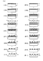
- the negative-patterning process of the present invention according to the three-layer resist method as mentioned above is done as following (refer to FIG. 1 ).
- the organic underlayer film 2 is formed on the body to be processed 1 by a spin coating method ( FIG. 1 (I-A)). It is desired that the organic under layer film 2 have high etching resistance because this acts as a mask during etching of the body to be processed 1; and it is also desired that this undergo crosslinking by heat or an acid after forming by spin coating because mixing with the silicon-containing film of the upper layer is undesirable.
- the silicon-containing resist under layer film 3 is formed by a spin coating method by using the composition of the present invention for a silicon-containing resist underlayer film ( FIG. 1 (I-B)), and then the photoresist film 4 is formed thereonto by a spin coating method ( FIG. 1 (I-C)).
- the silicon-containing resist underlayer film 3 can be formed by using a composition giving the silicon-containing resist underlayer film 3 whose pure-water contact angle in the part corresponding to the exposed area of the photoresist film 4 is in the range of 40 degrees or more to lower than 70 degrees after exposure.
- the photoresist film 4 is subjected to a usual pattern exposure, by using the mask 5, using a light source P corresponding to the photoresist film 4, such as, for example, a KrF excimer laser beam, an ArF excimer laser beam, an F 2 laser beam, and an EUV beam, to form a pattern preferably by any of a photolithography with the wavelength ranging from 10 nm or more to 300 nm or less, a direct drawing by an electron beam, and a nanoimprinting, or a combination of them ( FIG. 1 (I-D)); and thereafter, heat treatment thereof under the condition matching with each photoresist film ( FIG. 1 (I-E)), development by the organic solvent development (negative development), and then, as appropriate, rinsing are performed to obtain the negative resist pattern 4a ( FIG. 1 (I-F)).
- a light source P corresponding to the photoresist film 4 such as, for example, a KrF excimer laser beam, an ArF excimer laser
- this negative resist pattern 4a as an etching mask, etching is carried out under the dry etching condition that the etching speed of the silicon-containing resist underlayer film 3 is significantly faster relative to the photoresist film, for example, by dry etching using a fluorine-based gas plasma.
- the silicon-containing resist underlayer film pattern of negative type 3a can be obtained without substantially receiving an effect of pattern change due to side etching of the resist film ( FIG. 1 (I-G)).
- the organic underlayer film 2 is dry-etched under the dry etching condition that the etching speed of the organic resist underlayer film is significantly faster relative to the substrate having the silicon-containing resist underlayer film pattern of negative type 3a having the transferred negative resist pattern 4a obtained above, for example, by a reactive dry etching with a gas plasma containing oxygen or by a reactive dry etching with a gas plasma containing hydrogen and nitrogen.
- the organic underlayer film pattern of negative type 2a is obtained, while at the same time, the uppermost photoresist film is usually lost ( FIG. 1 (I-H)).
- the body to be processed 1 can be dry-etched with high precision by using, for example, a fluorine-based dry etching or a chlorine-based dry etching to transfer the negative pattern 1a to the body to be processed 1 ( FIG. 1 (I-I)).
- an organic hard mask formed by a CVD method may also be used instead of the organic underlayer film 2.
- the body to be processed can be processed by the procedure similar to the above procedure.
- the present invention provides a patterning process, wherein an organic underlayer film is formed on a body to be processed by using an application-type composition for the organic underlayer film, on this organic underlayer film is formed a silicon-containing resist underlayer film by using the composition for forming the silicon-containing resist underlayer film, on this silicon-containing resist underlayer film is formed a photoresist film by using a chemically amplified resist composition, the photoresist film is exposed to a high energy beam after heat treatment, a positive pattern is formed by dissolving an exposed area of the photoresist film by using an alkaline developer, pattern transfer is made onto the silicon-containing resist underlayer film by dry-etching by using the photoresist film having the positive pattern as a mask, pattern transfer is made onto the organic underlayer film by dry-etching by using the silicon-containing resist underlayer film having the transferred pattern as a mask, and then pattern transfer is made onto the body to be processed by dry-etching by using the organic underlayer film having the transferred pattern as a mask.
- a patterning process wherein an organic hard mask mainly comprising carbon is formed on a body to be processed by a CVD method, on this organic hard mask is formed a silicon-containing resist underlayer film by using the composition for forming the silicon-containing resist underlayer film, on this silicon-containing resist underlayer film is formed a photoresist film by using a chemically amplified resist composition, the photoresist film is exposed to a high energy beam after heat treatment, a positive pattern is formed by dissolving an exposed area of the photoresist film by using an alkaline developer, pattern transfer is made onto the silicon-containing resist underlayer film by dry-etching by using the photoresist film having the positive pattern as a mask, pattern transfer is made onto the organic hard mask by dry-etching by using the silicon-containing resist underlayer film having the transferred pattern as a mask, and then pattern transfer is made onto the body to be processed by dry-etching by using the organic hard mask having the transferred pattern as a mask.
- change of the contact angle in a part of the silicon-containing resist underlayer film corresponding to an unexposed area of the exposed photoresist film is 10 degree or less as compared with before photo-exposure. If difference of the contact angles between an unexposed area of the photoresist film and a part of the silicon-containing resist underlayer film corresponding to this area is 10 degrees or less, good adhesion can be realized in the positive development; and as a result, a fine pattern can be formed.
- the photoresist film is not particularly restricted provided that the film is of a chemically amplifying type and a positive pattern can be formed by development using an alkaline developer.
- a positive pattern can be formed by development using an alkaline developer.
- body to be processed, organic underlayer film, and organic hard mask may be the same as those explained in the negative patterning process.
- PEB post-exposure bake
- TMAH tetramethylammonium hydroxide
- the positive-patterning process of the present invention according to the three-layer resist method as mentioned above is done as following (refer to FIG. 1 ).
- the organic underlayer film 2 is formed on the body to be processed 1 by a spin coating method ( FIG. 1 (II-A)). It is desired that the organic underlayer film 2 has high etching resistance because this acts as a mask during etching of the body to be processed 1; and it is also desired that this undergoes crosslinking by heat or an acid after forming by spin coating because mixing with the silicon-containing resist underlayer film of the upper layer is undesirable.
- the silicon-containing resist underlayer film 3 is formed by a spin coating method by using the composition of the present invention for forming a silicon-containing resist underlayer film ( FIG. 1 (II-B)), and then the photoresist film 4 is formed thereonto by a spin coating method ( FIG. 1 (II-C)).
- the silicon-containing resist underlayer film 3 can be formed by using a composition giving the silicon-containing resist underlayer film 3 whose pure-water contact angle in the part corresponding to the exposed area of the photoresist film 4 is in the range of 40 degrees or more to lower than 70 degrees after exposure.
- the photoresist film 4 is subjected to a usual pattern exposure using a light source P corresponding to the photoresist film 4, such as, for example, a KrF excimer laser beam, an ArF excimer laser beam, an F 2 laser beam, and an EUV beam, to form a pattern preferably by any of a photolithography with the wavelength ranging from 10 nm or more to 300 nm or less, a direct drawing by an electron beam, and a nanoimprinting, or a combination of them ( FIG. 1 (II-D)); and thereafter, heat treatment thereof under the condition matching with each photoresist film ( FIG. 1 (II-E)), development by the alkaline developer, and then, as appropriate, rinsing are performed to obtain the positive resist pattern 4b ( FIG. 1 (II-F)).
- a light source P corresponding to the photoresist film 4 such as, for example, a KrF excimer laser beam, an ArF excimer laser beam, an F 2
- this negative resist pattern 4b as an etching mask, etching is carried out under the dry etching condition that the etching speed of the silicon-containing resist underlayer film 3 is significantly faster relative to the photoresist film, for example, by dry etching using a fluorine-based gas plasma.
- the silicon-containing resist underlayer film pattern of positive type 3b can be obtained without substantially receiving an effect of pattern change due to side etching of the resist film ( FIG. 1 (II-G)).
- the organic underlayer film 2 is dry-etched under the dry etching condition that the etching speed of the organic resist underlayer film 2 is significantly faster relative to the substrate having the silicon-containing resist underlayer film pattern 3b having the transferred positive resist pattern obtained above, for example, by a reactive dry etching with a gas plasma containing oxygen or by a reactive dry etching with a gas plasma containing hydrogen and nitrogen.
- the organic uneder layer film pattern of positive type 2b is obtained, while at the same time, the uppermost photoresist film is usually lost ( FIG. 1 (II-H)).
- the body to be processed 1 can be dry-etched with high precision by using, for example, a fluorine-based dry etching or a chlorine-based dry etching to transfer the positive pattern 1b to the body to be processed 1 ( FIG. 1 (II-I)).
- an organic hard mask formed by a CVD method may also be used instead of the organic underlayer film 2.
- the body to be processed 1 can be processed by the procedure similar to the above procedure.
- Synthesis Examples A-2 to A-20 and Synthesis Examples A-24 to A-25 were carried out under the conditions similar to those of Synthesis Example A-1 to obtain respective intended products. Meanwhile, in Synthesis Examples A-24 and A-25, a constituting unit derived from the general formula (2) is not contained; and thus, they are not the component (A) of the composition of the present invention.
- each of the silicon-containing compounds (A-1) to (A-25) obtained in the foregoing synthesis examples as the component (A), each of the silicon-containing compounds (B-1) to (B-8) obtained in the foregoing synthesis examples as the component (B), a thermal crosslinking accelerator, a photoacid generator, an acid, a solvent, and water were mixed with the respective ratios shown in Table 3; and then, the resulting mixture was filtrated through a 0.1- ⁇ m filter made of a fluorinated resin to obtain respective composition solutions Sol.1 to Sol.44 for forming a silicon-containing resist underlayer film.
- Sol.1 to Sol.42 are used for Examples of the present invention, and Sol.43 and Sol.44, not containing the component (A) of the present invention, are used for Comparative Examples. Further, Film-43 and Film-44 prepared from Sol.43 and Sol.44 are shown in Comparative Examples.
- composition solutions Sol.1 to Sol.44 for forming a resist underlayer film were applied on a substrate and then heated at 240°C for 60 seconds to obtain respective silicon-containing resist underlayer films Film-1 to Film-44 having film thickness of 35 nm; and then, the contact angle thereof to pure water (CA1) was measured (Table 4).
- composition solutions Sol.1 to Sol.44 for forming a silicon-containing resist underlayer film were applied onto a silicon wafer and then heated at 240°C for 60 seconds to obtain respective silicon-containing resist underlayer films Film-1 to Film-44 having film thickness of 35 nm.
- ArF resist solution shown in Table 9 (PR-1) was applied onto it was applied the ArF resist solution shown in Table 9 (PR-1), and then baked at 100°C for 60 seconds to form a photoresist film having film thickness of 100 nm.
- entirety of the photoresist film was removed by rinsing with propylene glycol monomethyl ether (PGME) to obtain a film that is equivalent to the silicon-containing resist underlayer film corresponding to an unexposed area of the unexposed photoresist film.
- Contact angles of these films to pure water (CA2) were measured (Table 5).
- composition solutions Sol.1 to Sol.44 for forming a silicon-containing resist underlayer film were applied onto a silicon wafer and then heated at 240°C for 60 seconds to obtain respective silicon-containing resist underlayer films Film-1 to Film-44 having film thickness of 35 nm.
- ArF resist solution for the negative development shown in Table 12 (PR-3) was applied onto it was applied the ArF resist solution for the negative development shown in Table 12 (PR-3), and then baked at 100°C for 60 seconds to form a photoresist film having film thickness of 100 nm.
- the photoresist film was applied with the immersion top coat shown in Table 10 (TC-1), and baked at 90°C for 60 seconds to form a top coat having film thickness of 50 nm.
- composition solutions Sol.1 to Sol.44 for forming a silicon-containing resist underlayer film were applied onto a silicon wafer and then heated at 240°C for 60 seconds to obtain respective silicon-containing underlayer films Film-1 to Film-44 having film thickness of 35 nm.
- ArF resist solution for the negative development shown in Table 12 (PR-3) was applied onto it was applied the ArF resist solution for the negative development shown in Table 12 (PR-3), and then baked at 100°C for 60 seconds to form a photoresist film having film thickness of 100 nm.
- the photoresist film was applied with the immersion top coat shown in Table 10 (TC-1), and then baked at 90°C for 60 seconds to form a top coat having film thickness of 50 nm.
- Each ArF resist solution for the negative development shown in Table 12 was applied and then baked at 100°C for 60 seconds to prepare the photoresist film having film thickness of 100 nm; and then, contact angle thereof to pure water was measured. Then, entirety of this resist film was exposed by using an ArF exposure instrument (NSR-S610C, manufactured by Nikon Corp.), baked at 100°C for 60 seconds (PEB), spin-dried after rinsing with diisoamyl ether, and then baked at 100°C for 20 seconds to remove the rinsing solvent by evaporation to obtain the ArF resist film corresponding to the patterned area not having the acid-labile group at the time of negative development. Contact angle thereof to pure water was measured (Table 8).
- Example 14 By following the procedures similar to those of Example 2 except that ArF resists and developers shown below were used instead of the developer (butyl acetate) used in Example 2, the negative 43-nm 1:1 line-and-space pattern of Film-11 was obtained by using the composition solution Sol.11 for forming a resist underlayer film. These results are shown in Table 14. By using these various developers, a resist pattern having a vertical profile of its cross section could be obtained (Examples 3-1 to 3-6 ).
- Pattern etching test positive pattern
- Example 1 silicon-containing resist underlayer films Film-11 to Film-40 and Film-43 were prepared; and onto each of these silicon-containing resist underlayer films was applied the ArF resist solution for the positive development shown in Table 9 (PR-1), and then baked at 110°C for 60 seconds to form the photoresist film having film thickness of 100 nm. Onto the photoresist film was applied the immersion top coat shown in Table 10 (TC-1), and then baked at 90°C for 60 seconds to form the top coat having film thickness of 50 nm (Examples 4-1 to 4-10, 4-21 to 4-30, and Comparative Example 4-1).
- the ArF resist solution for positive development shown in Table 9 was applied onto the silicon-containing resist underlayer film, and then baked at 110°C for 60 seconds to form the photoresist film having film thickness of 100 nm (Examples 4-11 to 4-20 ).
- the silicon-containing resist underlayer film was dry-etched under the following condition (1) and then dry-etched under the following condition (2) to transfer the pattern onto the spin-on carbon film.
- Pattern profile of cross section of the obtained pattern was measured with an electron microscope (S-9380, manufactured by Hitachi, Ltd.) and pattern roughness was measured with an electron microscope (CG 4000, manufactured by Hitachi High-technologies Corp.); and they were compared as summarized in Table 15.
- Pattern etching test negative pattern
- silicon-containing resist underlayer films Film-11 to Film-40 and Film-43 were prepared; and onto each of these silicon-containing resist underlayer films was applied the ArF resist solution for the negative development shown in Table 12 (PR-3 and PR-4), and then baked at 100°C for 60 seconds to form the photoresist film having film thickness of 100 nm.
- Onto the photoresist film was applied the immersion top coat shown in Table 10 (TC-1), and then baked at 90°C for 60 seconds to form the top coat having film thickness of 50 nm (Examples 5-1 to 5-20, 5-29 to 5-30, and Comparative Example 5-1).
- the ArF resist solution for the negative development shown in Table 12 was applied onto the silicon-containing resist underlayer film, and then baked at 110°C for 60 seconds to form the photoresist film having film thickness of 100 nm ( Examples 5-21 to 5-28 ).
- the silicon-containing resist underlayer film was dry-etched under the above condition (1) and then dry-etched under the above condition (2) to transfer the pattern onto the spin-on carbon film.
- Pattern profile of cross section of the obtained pattern was measured with an electron microscope (S-9380, manufactured by Hitachi, Ltd.) and pattern roughness was measured with an electron microscope (CG 4000, manufactured by Hitachi High-technologies Corp.); and they were compared as summarized in Table 16.
- the present invention can provide (i) the composition for forming a silicon-containing resist underlayer film that is applicable not only to a resist pattern formed of a hydrophilic organic compound obtained by a negative development but also a resist pattern formed of a hydrophobic compound obtained by a conventional positive development, and (ii) the patterning process using this composition.
Landscapes
- Chemical & Material Sciences (AREA)
- Physics & Mathematics (AREA)
- General Physics & Mathematics (AREA)
- Chemical Kinetics & Catalysis (AREA)
- Organic Chemistry (AREA)
- Engineering & Computer Science (AREA)
- Materials Engineering (AREA)
- Life Sciences & Earth Sciences (AREA)
- Structural Engineering (AREA)
- Wood Science & Technology (AREA)
- Architecture (AREA)
- Health & Medical Sciences (AREA)
- Medicinal Chemistry (AREA)
- Polymers & Plastics (AREA)
- Materials For Photolithography (AREA)
- Photosensitive Polymer And Photoresist Processing (AREA)
- Polymers With Sulfur, Phosphorus Or Metals In The Main Chain (AREA)
Abstract
(A) a silicon-containing compound obtained by a hydrolysis-condensation reaction of a mixture containing, at least, one or more hydrolysable silicon compound shown by the following general formula (1) and one or more hydrolysable compound shown by the following general formula (2), and (B) a silicon-containing compound obtained by a hydrolysis-condensation reaction of a mixture containing, at least, one or more hydrolysable silicon compound shown by the following general formula (3) and one or more hydrolysable silicon compound shown by the following general formula (4). There can be provided a composition for forming a resist underlayer film applicable not only to a resist pattern obtained in a negative development but also to a resist pattern obtained in a conventional positive development, and a patterning process using this composition.
R1 m1R2 m2R3 m3Si(OR)(4-m1-m2-m3) (1)
U(OR4)m4(OR5)m5 (2)
R6 m6R7 m7R8 m8Si(OR9)(4-m6-m7-m8) (3)
Si(OR10)4 (4)
Description
- The present invention relates to a composition for forming a silicon-containing resist underlayer film and a patterning process using the same.
- In 1980s, a g-line (436 nm) or an i-line (365 nm) of a mercury lamp was used as an exposure light to be used in a resist pattern forming. As a mean for further miniaturization, a method of shifting to a shorter wavelength of an exposing light was assumed to be effective. As a result, in a mass production process after DRAM (Dynamic Random Access Memory) with 64-megabits (0.25 µm or less of a processing dimension) in 1990s, a KrF excimer laser (248 nm), a shorter wavelength than an i-line (365 nm), was used in place of an i-line as an exposure light source. However, in production of DRAM with an integration of 256 M, 1 G and higher which require further miniaturized process technologies (process dimension of 0.2 µm or less), a light source with a further short wavelength is required, and thus a photo lithography using an ArF excimer laser (193 nm) has been investigated seriously since about a decade ago. At first, an ArF lithography was planned to be applied to a device starting from a 180 nm node device, but a KrF excimer laser lithography lived long to a mass production of a 130 nm node device, and thus a full-fledged application of an ArF lithography will start from a 90 nm node. Further, a study of a 65 nm node device by combining with a lens having an increased NA till 0.9 is now underway.
Further shortening of wavelength of an exposure light is progressing towards the next 45 nm node device, and for that an F2 lithography with a 157 nm wavelength became a candidate. However, there are many problems in an F2 lithography; an increase in cost of a scanner due to the use of a large quantity of expensive CaF2 single crystals for a projector lens, extremely poor sustainability of a soft pellicle, which leads to a change of an optical system due to introduction of a hard pellicle, a decrease in an etching resistance of a resist film, and the like. Because of these problems, it has been abandon the development of an F2 lithography and introduced an ArF immersion lithography earlier. - In the ArF liquid immersion lithography, water having a refractive index of 1.44 is inserted between the projection lens and a wafer by a partial filling manner to enable highspeed scanning, thereby allowing to conduct mass-production of 45nm node devices by a lens having an NA on the order of 1.3.
- Exemplary candidates of lithography techniques for 32nm nodes include extreme ultraviolet(EUV) lithography at a wavelength of 13.5nm. Then, exemplary objects accompanying to the EUV lithography are to increase an output of laser, enhance a sensitivity of resist film, enhance a resolution, decrease a line edge roughness (LER), achieve a defect-free MoSi laminate mask, lower aberrations of a reflecting mirror, for example, thereby leaving a pile of objects to be attained.
- Another candidate of 32nm nodes is a high refractive index liquid immersion lithography, the development of which has been abandoned, due to lower transmittance of LuAG as a candidate of high refractive index lens therefor, and due to failure of achievement of a refractive index of a liquid to be increased up to a targeted value of 1.8.
- As mentioned above, a photo-exposure method used as a general-purpose technology is reaching an inherent limit of its resolution due to wavelength of a light source. Accordingly, in recent years, an organic solvent development, with which a very fine hole pattern that cannot be accomplished by a conventional patterning process with a positive tone using an alkaline developer is obtained by a patterning process with a negative tone using an organic solvent developer, has been receiving an attention again. This is a process to form a negative pattern by an organic solvent developer by using a high resolution positive resist composition. In addition, investigation is being carried out to obtain twofold resolution by combining two developments of an alkaline development and an organic solvent development.
- Usable as an ArF resist composition for development in a negative tone by an organic solvent like this, is a positive ArF resist composition of a conventional type, and examples of patterning processes therefor are shown in Japanese Patent Laid-Open (kokai) No.
2008-281974 2008-281980 2009-53657 - As one method to transfer the thus formed negative-tone pattern to a substrate, multi-layer resist process have been used. The methods are configured to: interpose an intermediate film, for example a resist underlayer film containing silicon atom, having an etching selectivity different from that of a photoresist film, i.e., a resist upper layer film, between the resist upper layer film and a body to be processed; obtain a pattern in the resist upper layer film; thereafter transfer the pattern to the resist underlayer film by dry etching by using the obtained resist upper layer film pattern as a dry etching mask; and further transfer the pattern onto the body to be processed by dry etching by using the obtained pattern of the resist underlayer film as a dry etching mask.
- Examples of silicon-containing resist underlayer films to be used in the above-described multi-layer resist process include silicon-containing inorganic films by CVD, such as SiO2 films (Japanese Patent Laid-Open (kokai) No.
H7-183194 H7-181688 2007-302873 2005-520354 - Contrary to a positive development (alkaline development) in which a resist pattern formed of a hydrophobic compound not soluble in an alkaline developer is obtained, in a negative development (organic solvent development), a resist pattern formed of a hydrophilic organic compound containing, in high concentration, an acidic group such as a carboxyl group generated by a deprotection reaction is obtained; and thus, performance of a photo resist cannot be realized sufficiently with a conventional resist underlayer film for an alkaline development.
- On the other hand, if a resist underlayer film used in a negative development is different from a resist underlayer film used in a positive development, piping equipment solely dedicated to respective developments are necessary; and thus, this is economically irrational.
- The present invention was made in view of the problems as mentioned above, and has an object to provide (i) a composition for forming a silicon-containing resist underlayer film applicable not only to a resist pattern formed of a hydrophilic organic compound obtained in a negative development but also to a resist pattern formed of a hydrophobic compound obtained in a conventional positive development, and (ii) a patterning process using this composition.
- Namely, the present invention provides a composition for forming a silicon-containing resist underlayer film comprising:
- (A) a silicon-containing compound obtained by a hydrolysis-condensation reaction of a mixture containing, at least, one or more hydrolysable silicon compound shown by the following general formula (1) and one or more hydrolysable compound shown by the following general formula (2),
R1 m1R2 m2R3 m3Si (OR) (4-m1-m2-m3) (1)
wherein, R represents a hydrocarbon group having 1 to 6 carbon atoms; at least one of R1, R2, and R3 is an organic group containing a hydroxyl group or a carboxyl group, the groups being substituted with an acid-labile group, while the other is a hydrogen atom or a monovalent organic group having 1 to 30 carbon atoms; and m1, m2, and m3 represent 0 or 1 and satisfy 1≤m1+m2+m3≤3;
U(OR4)m4(OR5)m5 (2)
wherein, R4 and R5 represent an organic group having 1 to 30 carbon atoms, and m4+m5 is the same number as the number determined by valency of U; m4 and m5 represent an integer of 0 or more; and the U is an element belonging to groups of III, IV, or V in a periodic table except for carbon and silicon; - (B) a silicon-containing compound obtained by a' hydrolysis-condensation reaction of a mixture containing, at least, one or more hydrolysable silicon compound shown by the following general formula (3) and one or more hydrolysable silicon compound shown by the following general formula (4),
R6 m6R7 m7R8 m8Si (OR9)(4-m6-m7-m8) (3)
wherein, R9 represents an alkyl group having 1 to 6 carbon atoms, and each R6, R7, and R8 represents a hydrogen atom or a monovalent organic group having 1 to 30 carbon atoms; and m6, m7, and m8 represent 0 or 1 and satisfy 1≤m6+m7+m3≤8; and
Si(OR10)4 (4)
wherein, R10 represents an alkyl group having 1 to 6 carbon atoms. - In a positive development, it has been experimentally known that, if a contact angle of a resist pattern obtained after photo-exposure is made coincident with a contact angle of a resist underlayer film, it is effective to enhance adhesion and to lower roughness in a resist pattern. However, in a negative pattern obtained by a negative development, when comparison is made on film properties between the photoresist film before photo-exposure and the resist pattern after photo-exposure, amount of a hydrophilic group such as a carboxyl group and a phenolic hydroxyl group due to elimination of an acid-labile group caused by an acid generated by the photo-exposure is increased in the resist pattern after the photo-exposure; and as a result, a contact angle of the resist pattern is shifted toward a hydrophilic side, i.e., a lower side, as compared with that before the photo-exposure. Because of this, it was found, in a conventional underlayer film for positive resist whose contact angle is made coincident with that of a photoresist film before the photo-exposure, discrepancy from the contact angle of the negative pattern is generated thereby causing pattern fall and an adverse effect in roughness. In other words, if the contact angle in a part of the resist underlayer film corresponding to an exposed area of the photoresist film is approximated to the contact angle of the negative pattern of the photoresist and the contact angle in the part corresponding to an unexposed area thereof is approximated to the contact angle of the positive pattern of the photoresist, a resist underlayer film applicable to both the negative and positive development processes can be obtained. Accordingly, the composition for forming a silicon-containing resist underlayer film as mentioned above becomes a composition for forming a silicon-containing resist underlayer film giving a silicon-containing resist underlayer film that has an enhanced adhesion with a photoresist pattern and does not cause pattern fall even in a pattern with a narrow line in any of the processes.
- In addition, it is preferable that mass ratio of the component (A) to the component (B) satisfies (B) / (A)≥1.
- Further, of the constituting units derived from the general formula (3) and the general formula (4) in the component (B), it is preferable that mole ratio of the constituting unit derived from the general formula (4) is 50% or more by mole.
- By using appropriate silicon-containing compounds in the component (A) and the component (B) used in the present invention and selecting appropriate mass ratio thereof as mentioned above, a composition being capable of forming a resist underlayer film not only having excellent storage stability and adhesion but also not changing patterning properties in both the negative and positive developments can be obtained.
- In addition, it is preferable that the U of the general formula (2) is any of boron, aluminum, gallium, yttrium, germanium, titanium, zirconium, hafnium, bismuth, tin, phosphorous, vanadium, arsenic, antimony, niobium, and tantalum.
- As mentioned above, by introducing the foregoing elements, optimization of etching selectivity between the photoresist and the resist underlayer film becomes possible so that a composition formable the resist underlayer film having excellent size stability during dry etching may be obtained.
- In addition, the present invention provides a patterning process, wherein an organic underlayer film is formed on a body to be processed by using an application-type composition for the organic underlayer film, on this organic underlayer film is formed a silicon-containing resist underlayer film by using the composition for forming the silicon-containing resist underlayer film, on this silicon-containing resist underlayer film is formed a photoresist film by using a chemically amplified resist composition, the photoresist film is exposed to a high energy beam after heat treatment, a positive pattern is formed by dissolving an exposed area of the photoresist film by using an alkaline developer, pattern transfer is made onto the silicon-containing resist underlayer film by dry-etching by using the photoresist film having the positive pattern as a mask, pattern transfer is made onto the organic underlayer film by dry-etching by using the silicon-containing resist underlayer film having the transferred pattern as a mask, and then pattern transfer is made onto the body to be processed by dry-etching by using the organic underlayer film having the transferred pattern as a mask.
- Further, the present invention provides a patterning process, wherein an organic hard mask mainly comprising carbon is formed on a body to be processed by a CVD method, on this organic hard mask is formed a silicon-containing resist underlayer film by using the composition for forming the silicon-containing resist underlayer film, on this silicon-containing resist underlayer film is formed a photoresist film by using a chemically amplified resist composition, the photoresist film is exposed to a high energy beam after heat treatment, a positive pattern is formed by dissolving an exposed area of the photoresist film by using an alkaline developer, pattern transfer is made onto the silicon-containing resist underlayer film by dry-etching by using the photoresist film having the positive pattern as a mask, pattern transfer is made onto the organic hard mask by dry-etching by using the silicon-containing resist underlayer film having the transferred pattern as a mask, and then pattern transfer is made onto the body to be processed by dry-etching by using the organic hard mask having the transferred pattern as a mask.
- When patterning is done by a positive development using the composition of the present invention for a resist underlayer film, by optimizing combination with the CVD film or the organic underlayer film in the way as mentioned above, a pattern formed with a photoresist can be formed on a substrate without causing size difference.
- In addition, in photo-exposure of the photoresist film, it is preferable that change of the contact angle in a part of the silicon-containing resist underlayer film corresponding to an unexposed area of the exposed photoresist film is 10 degree or less as compared with before photo-exposure.
- If change amount of the contact angle is like this, difference of contact angles between an unexposed area of the exposed photoresist film and a part of the silicon-containing resist underlayer film corresponding to this unexposed area of the exposed photoresist film becomes 10 degrees or less thereby leading to good adhesion in the positive development; and as a result, a fine pattern can be formed.
- Further, the present invention provides a patterning process, wherein an organic underlayer film is formed on a body to be processed by using an application-type composition for the organic underlayer film, on this organic underlayer film is formed a silicon-containing resist underlayer film by using the composition for forming the silicon-containing resist underlayer film, on this silicon-containing resist underlayer film is formed a photoresist film by using a chemically amplified resist composition, the photoresist film is exposed to a high energy beam after heat treatment, a negative pattern is formed by dissolving an unexposed area of the photoresist film by using an organic solvent developer, pattern transfer is made onto the silicon-containing resist underlayer film by dry-etching by using the photoresist film having the negative pattern as a mask, pattern transfer is made onto the organic underlayer film by dry-etching by using the silicon-containing resist underlayer film having the transferred pattern as a mask, and then pattern transfer is made onto the body to be processed by dry-etching by using the organic underlayer film having the transferred pattern as a mask.
- In addition, the present invention provides a patterning process, wherein an organic hard mask mainly comprising carbon is formed on a body to be processed by a CVD method, on this organic hard mask is formed a silicon-containing resist underlayer film by using the composition for forming the silicon-containing resist underlayer film, on this silicon-containing resist underlayer film is formed a photoresist film by using a chemically amplified resist composition, the photoresist film is exposed to a high energy beam after heat treatment, a negative pattern is formed by dissolving an unexposed area of the photoresist film by using an organic solvent developer, pattern transfer is made onto the silicon-containing resist underlayer film by dry-etching by using the photoresist film having the negative pattern as a mask, pattern transfer is made onto the organic hard mask by dry-etching by using the silicon-containing resist underlayer film having the transferred pattern as a mask, and then pattern transfer is made onto the body to be processed by dry-etching by using the organic hard mask having the transferred pattern as a mask.
- When a negative pattern is formed by using the composition of the present invention for forming a silicon-containing resist underlayer film, by optimizing combination with the CVD film or the organic underlayer film in the way as mentioned above, a pattern formed with a photoresist can be formed on a substrate without causing size difference.
- Further, in photo-exposure of the photoresist film, it is preferable that the contact angle of a part of the silicon-containing resist underlayer film corresponding to an exposed area of the exposed photoresist film is decreased by 10 degrees or more after photo-exposure as compared with before photo-exposure.
- The contact angle of the resist pattern after photo-exposure is shifted toward a hydrophilic side, i.e., a lower side than before the photo-exposure; and thus, if the contact angle of the part of the silicon-containing resist underlayer film corresponding to the exposed area of the exposed photoresist film is lowered by 10 degrees or more as compared with before photo-exposure, difference with the contact angle of the resist pattern after the negative development becomes small thereby enhancing adhesion and prohibiting pattern fall; and as a result, a fine pattern can be formed.
- In addition, in the negative patterning process and the positive patterning process, it is preferable that the body to be processed is a substrate for a semiconductor device, or the substrate for a semiconductor device coated, as a layer to be processed, with any of a metal film, a metal carbide film, a metal oxide film, a metal nitride film, a metal oxycarbide film, and a metal oxynitride film.
- Further, in the negative patterning process and the positive patterning process, it is preferable that the metal that constitutes the body to be processed is silicon, titanium, tungsten, hafnium, zirconium, chromium, germanium, copper, aluminum, iron, or an alloy of these metals.
- According to the patterning process of the present invention, a pattern can be formed by processing the body to be processed as mentioned above.
- When the resist underlayer film formed by using the composition of the present invention for forming a silicon-containing resist underlayer film is used, a resist pattern with excellent adhesion with the resist underlayer film, without pattern fall and with good surface roughness can be obtained in both the positive development (alkaline development) and the negative development (organic solvent development). In addition, in this resist underlayer film, high etching selectivity with an organic material can be obtained; and thus, the formed photoresist pattern can be transferred successively to the silicon-containing resist underlayer film and then to the organic underlayer film or the CVD organic hard mask by using a dry etching process. Especially as the manufacturing process of a semiconductor device is progressing toward further miniaturization in recent years, in order to prohibit pattern fall after development, a thickness of the photoresist film is prone to thinner whereby pattern transfer to the resist underlayer film is becoming difficult. However, if the composition of the present invention for forming a silicon-containing resist underlayer film is used, deformation of the photoresist pattern during dry etching can be suppressed even if a thin photoresist film is used as an etching mask, so that this pattern can be transferred to a substrate with high precision.
- In addition, in practical manufacturing process of a semiconductor device, all the patterning processes are not changed from the positive development to the negative development, but only part of an ultrafine process is changed; and thus, it may be assumed that the existing positive development process remains unchanged. In this case, if a resist underlayer film solely dedicated to each the negative development and the positive development are used, equipment may become complicated and quality control may become cumbersome. Accordingly, when a composition for forming a silicon-containing resist underlayer film usable in both the positive and the negative processes, like the one in the present invention, is used, rational management may be possible in both equipment and quality control.
-
Fig. 1 is a flow chart showing one embodiment of a patterning process according to the present invention. - In a positive photoresist, conventionally, film properties of the photoresist film before photo-exposure and film properties of the pattern formed by an alkaline development after photo-exposure (hereinafter this pattern is called "positive pattern") have been the same. And thus, to enhance adhesion of the positive pattern with the resist underlayer film, contact angle of the photoresist to pure water and contact angle of the resist underlayer film to pure water (hereinafter "contact angle to pure water" is called "contact angle") were approximated; and this approach has been effective to enhance adhesion of the positive pattern with the resist underlayer film and to lower the roughness as well.
- However, in the pattern obtained by a negative development (hereinafter, this pattern is called "negative pattern"), when comparison is made on film properties between the photoresist film before photo-exposure and the negative pattern after photo-exposure, in the negative pattern, an acid-labile group is eliminated by an acid generated by the photo-exposure thereby increasing amount of hydrophilic groups such as a carboxyl group and a phenolic hydroxyl group; and as a result, the contact angle is shifted toward a more hydrophilic side, i.e., a lower side, than that of the photoresist film before the photo-exposure. Because of this, it was found, in the patterning process in which both the negative development and the positive development are used, when a conventional resist underlayer film for a positive development whose contact angle is made coincident with that of a photoresist film before the photo-exposure is used as it is, discrepancy from the contact angle of the negative pattern after the photo-exposure is generated thereby causing fall of the negative pattern and an adverse effect in roughness.
- Accordingly, inventors of the present invention found that, by utilizing the fact that the positive pattern is the unexposed photoresist film area and the negative pattern is the exposed photoresist film area, if the contact angle before the photo-exposure was approximated to the contact angle of the unexposed photoresist film part to pure water and the contact angle in the exposed area was approximated to the contact angle of the resist film after the photo-exposure, the resist underlayer film having optimum surface conditions in any of the processes could be obtained. With this finding, the inventors carried out extensive investigation on a composition for forming a silicon-containing resist underlayer film whose contact angle decreases only in the exposed area; and as a result, the inventors found that, when a polymer having an acid-labile group and a polymer not having this group were blended in an appropriate mixing ratio, a composition for forming a silicon-containing resist underlayer film whose contact angle decreased only in the exposed area could be obtained thereby accomplishing the present invention.
- In addition, by controlling the constituting element in the resist underlayer film containing an organic group which is a driving force to change the contact angle of the resist underlayer film part corresponding to the exposed area of the photoresist film, etching selectivity with the photoresist film could be optimized so that both etching performance and patterning performance could be satisfied.
- In the composition of the present invention for forming a silicon-containing resist underlayer film, when a silicon-containing compound containing a hydroxyl group or a carboxyl group, the groups being substituted with an acid-labile group, is mixed as the component (A) with a silicon-containing compound having excellent etching selectivity with the photoresist as the component (B), whereby localizing the component (A) on surface of the resist underlayer film, respective optimum surface contact angles during the time of the positive development and the negative development can be realized. Hereinafter, detailed explanation thereof will be described.
- The composition of the present invention for forming a silicon-containing resist underlayer film contains, as the component (A), a silicon-containing compound obtained by a hydrolysis-condensation reaction of a mixture containing, at least, one or more hydrolysable silicon compound shown by the following general formula (1) and one or more hydrolysable compound shown by the following general formula (2),
R1 m1R2 m2R3 m3Si (OR) (4-m1-m2-m3) (1)
wherein, R represents a hydrocarbon group having 1 to 6 carbon atoms; and at least one of R1, R2, and R3 is an organic group containing a hydroxyl group or a carboxyl group, the groups being substituted with an acid-labile group, while the other is a hydrogen atom or a monovalent organic group having 1 to 30 carbon atoms. m1, m2, and m3 represent 0 or 1 and satisfy 1≤m1+m2+m3≤3,
U(OR4)m4(OR5)m5 (2)
wherein, R4 and R5 represent an organic group having 1 to 30 carbon atoms, and m4+m5 is the same number as the number determined by valency of U. m4 and m5 represent an integer of 0 or more, and the U is an element belonging to groups of III, IV, or V in a periodic table except for carbon and silicon. - As to the hydrolysable silicon compound shown by the general formula (1) used as a raw material of the component (A), the compound containing two or three hydrolysable groups selected from a methoxy group, an ethoxy group, a propoxy group, and a butoxy group that are bonded to the silicon atom, as shown in the following structures, may be used.


- As to the hydrolysable compound shown by the general formula (2) used as a raw material of the component (A), the followings may be mentioned. In the case that the U is boron, illustrative examples of the hydrolysable compound shown by the general formula (2) include, as monomers, boron methoxide, boron ethoxide, boron propoxide, boron butoxide, boron amyloxide, boron hexyloxide, boron cyclopentoxide, boron cyclohexloxide, boron allyloxide, boron phenoxide, boron methoxyethoxide, boric acid, and boron oxide.
- When U is aluminum, examples of the hydrolysable compound shown by the formula (2) include, as monomers, aluminum methoxide, aluminum ethoxide, aluminum propoxide, aluminum butoxide, aluminum amyloxide, aluminum hexyloxide, aluminum cyclopentoxide, aluminum cyclohexyloxide, aluminum allyloxide, aluminum phenoxide, aluminum methoxyethoxide, aluminum ethoxyethoxide, aluminum dipropoxyethyl-acetoacetate, aluminum dibutoxyethyl-acetoacetate, aluminum propoxy-bis-ethyl-acetoacetate, aluminum butoxy-bis-ethyl-acetoacetate,
aluminum 2,4-pentanedionate, andaluminum - When U is gallium, examples of the hydrolysable compound shown by the formula (2) include, as monomers, gallium methoxide, gallium ethoxide, gallium propoxide, gallium butoxide, gallium amyloxide, gallium hexyloxide, gallium cyclopentoxide, gallium cyclohexyloxide, gallium allyloxide, gallium phenoxide, gallium methoxyethoxide, gallium ethoxyethoxide, gallium dipropoxyethyl-acetoacetate, gallium dibutoxyethyl-acetoacetate, gallium propoxy-bis-ethyl-acetoacetate, gallium butoxy-bis-ethyl-acetoacetate,
gallium 2,4-pentanedionate, andgallium - When U is yttrium, examples of the hydrolysable compound shown by the formula (2) include, as monomers, yttrium methoxide, yttrium ethoxide, yttrium propoxide, yttrium butoxide, yttrium amyloxide, yttrium hexyloxide, yttrium cyclopentoxide, yttrium cyclohexyloxide, yttrium allyloxide, yttrium phenoxide, yttrium methoxyethoxide, yttrium ethoxyethoxide, yttrium dipropoxyethyl-acetoacetate, yttrium dibutoxyethyl-acetoacetate, yttrium propoxy-bis-ethyl-acetoacetate, yttrium butoxy-bis-ethyl-acetoacetate,
yttrium 2,4-pentanedionate, andyttrium - When U is germanium, examples of the hydrolysable compound shown by the formula (2) include, as monomers, germanium methoxide, germanium ethoxide, germanium propoxide, germanium butoxide, germanium amyloxide, germanium hexyloxide, germanium cyclopentoxide, germanium cyclohexyloxide, germanium allyloxide, germanium phenoxide, germanium methoxyethoxide, and germanium ethoxyethoxide.
- When U is titanium, examples of the hydrolysable compound shown by the formula (2) include, as monomers, titanium methoxide, titanium ethoxide, titanium propoxide, titanium butoxide, titanium amyloxide, titanium hexyloxide, titanium cyclopentoxide, titanium cyclohexyloxide, titanium allyloxide, titanium phenoxide, titanium methoxyethoxide, titanium ethoxyethoxide, titanium dipropoxy-bisethyl-acetoacetate, titanium dibutoxy-bisethyl-acetoacetate, titanium dipropoxy-bis-2,4-pentanedionate, and titanium dibutoxy-bis-2,4-pentanedionate.
- When U is hafnium, examples of the hydrolysable compound shown by the formula (2) include, as monomers, hafnium methoxide, hafnium ethoxide, hafnium propoxide, hafnium butoxide, hafnium amyloxide, hafnium hexyloxide, hafnium cyclopentoxide, hafnium cyclohexyloxide, hafnium allyloxide, hafnium phenoxide, hafnium methoxyethoxide, hafnium ethoxyethoxide, hafnium dipropoxy-bisethyl-acetoacetate, hafnium dibutoxy-bisethyl-acetoacetate, hafnium dipropoxy-bis-2,4-pentanedionate, and hafnium dibutoxy-bis-2,4-pentanedionate.
- When U is tin, examples of the hydrolysable compound shown by the formula (2) include, as monomers, methoxy tin, ethoxy tin, propoxy tin, butoxy tin, phenoxy tin, methoxyethoxy tin, ethoxyethoxy tin,
tin 2,4-pentanedionate, andtin - When U is arsenic, examples of the hydrolysable compound shown by the formula (2) include, as monomers, methoxy arsenic, ethoxy arsenic, propoxy arsenic, butoxy arsenic, and phenoxy arsenic.
- When U is antimony, examples of the hydrolysable compound shown by the formula (2) include, as monomers, methoxy antimony, ethoxy antimony, propoxy antimony, butoxy antimony, phenoxy antimony, antimony acetate, and antimony propionate.
- When U is niobium, examples of the hydrolysable compound shown by the formula (2) include, as monomers, methoxy niobium, ethoxy niobium, propoxy niobium, butoxy niobium, and phenoxy niobium.
- When U is tantalum, examples of the hydrolysable compound shown by the formula (2) include, as monomers, methoxy tantalum, ethoxy tantalum, propoxy tantalum, butoxy tantalum, and phenoxy tantalum.
- When U is bismuth, examples of the hydrolysable compound shown by the formula (2) include, as monomers, methoxy bismuth, ethoxy bismuth, propoxy bismuth, butoxy bismuth, and phenoxy bismuth.
- When U is phosphorus, examples of the compounds represented by the formula (2) include, as monomers, trimethyl phosphite, triethyl phosphite, tripropyl phosphite, and diphosphorus pentoxide.
- When U is vanadium, examples of the compounds represented by the formula (2) include, as monomers, vanadium oxide-bis (2,4-pentanedionate),
vanadium 2,4-pentanedionate, vanadium tributoxide oxide, and vanadium tripropoxide oxide. - When U is zirconium, examples of the compounds represented by the formula (2) include, as monomers, methoxy zirconium, ethoxy zirconium, propoxy zirconium, butoxy zirconium, phenoxy zirconium, zirconium dibutoxide-bis (2,4-pentanedionate), and zirconium dipropoxide-bis (2,2,6,6-tetramethyl-3,5-heptanedionate).
- In the present invention, by introducing the foregoing elements as U of the general formula (2), etching selectivity between the photoresist film and the resist underlayer film formed by the composition of the present invention can be optimized; and as a result, a composition formable the resist underlayer film having excellent size stability during processing by dry etching can be obtained.
- In addition, compounds shown by the general formulae (3) and (4) used as raw materials of the component (B) as mentioned later may be used as a part of raw materials of the component (A).
- Amount of the general formula (1) in the component (A) is preferably 5% or more by mole, or more preferably 10% or more by mole. Amount of the general formula (2) in the component (A) is preferably 10% or more by mole, or more preferably 20% or more by mole. Amount of the general formulae (1) and (2) in the component (A) is preferably 50% or more by mole, or more preferably 55% or more by mole.
- The composition of the present invention for forming a silicon-containing resist underlayer film contains, as the component (B), a silicon-containing compound obtained by a hydrolysis-condensation reaction of a mixture containing, at least, one or more hydrolysable silicon compound shown by the following general formula (3) and one or more hydrolysable silicon compound shown by the following general formula (4). Component (B) is not particularly restricted, but the component preferably does not contain a hydroxyl group or a carboxyl group, the groups being substituted with an acid-labile group,
R6 m6R7 m7R8 m8Si (OR9) (4-m6-m7-m8) (3)
wherein, R9 represents an alkyl group having 1 to 6 carbon atoms, and each R6, R7, and R8 represents a hydrogen atom or a monovalent organic group having 1 to 30 carbon atoms. m6, m7, and m8 represent 0 or 1 and satisfy 1≤m6+m7+m8≤3,
Si(OR10)4 (4)
wherein, R10 represents an alkyl group having 1 to 6 carbon atoms. - As to the compound shown by the general formula (3) used as a raw material of the component (B), following compounds may be mentioned as illustrative examples thereof.
- Examples thereof include trimethoxysilane, triethoxysilane, tripropoxysilane, triisopropoxysilane, methyltrimethoxysilane, methyltriethoxysilane, methyltripropoxysilane, methyltriisopropoxysilane, ethyltrimethoxysilane, ethyltriethoxysilane, ethyltripropoxysilane, ethyltriisopropoxysilane, vinyltrimethoxysilane, vinyltriethoxysilane, vinyltripropoxysilane, vinyltriisopropoxysilane, propyltrimethoxysilane, propyltriethoxysilane, propyltripropoxysilane, propyltriisopropoxysilane, isopropyltrimethoxysilane, isopropyltriethoxysilane, isopropyltripropoxysilane, isopropyltriisopropoxysilane, butyltrimethoxysilane, butyltriethoxysilane, butyltripropoxysilane, butyltriisopropoxysilane, sec-butyltrimethoxysilane, sec-butyltriethoxysilane, sec-butyltripropoxysilane, sec-butyltriisopropoxysilane, t-butyltrimethoxysilane, t-butyltriethoxysilane, t-butyltripropoxysilane, t-butyltriisopropoxysilane, cyclopropyltrimethoxysilane, cyclopropyltriethoxysilane, cyclopropyltripropoxysilane, cyclopropyltriisopropoxysilane, cyclobutyltrimethoxysilane, cyclobutyltriethoxysilane, cyclobutyltripropoxysilane, cyclobutyltriisopropoxysilane, cyclopentyltrimethoxysilane, cyclopentyltriethoxysilane, cyclopentyltripropoxysilane, cyclopentyltriisopropoxysilane, cyclohexyltrimethoxysilane, cyclohexyltriethoxysilane, cyclohexyltripropoxysilane, cyclohexyltriisopropoxysilane, cyclohexenyltrimethoxysilane, cyclohexenyltriethoxysilane, cyclohexenyltripropoxysilane, cyclohexenyltriisopropoxysilane, cyclohexenylethyltrimethoxysilane, cyclohexenylethyltriethoxysilane, cyclohexenylethyltripropoxysilane, cyclohexenylethyltriisopropoxysilane, cyclooctyltrimethoxysilane, cyclooctyltriethoxysilane, cyclooctyltripropoxysilane, cyclooctyltriisopropoxysilane, cyclopentadienylpropyltrimethoxysilane, cyclopentadienylpropyltriethoxysilane, cyclopentadienylpropyltripropoxysilane, cyclopentadienylpropyltriisopropoxysilane, bicycloheptenyltrimethoxysilane, bicycloheptenyltriethoxysilane, bicycloheptenyltripropoxysilane, bicycloheptenyltriisopropoxysilane, bicycloheptyltrimethoxysilane, bicycloheptyltriethoxysilane, bicycloheptyltripropoxysilane, bicycloheptyltriisopropoxysilane, adamantyltrimethoxysilane, adamantyltriethoxysilane, adamantyltripropoxysilane, adamantyltriisopropoxysilane, phenyltrimethoxysilane, phenyltriethoxysilane, phenyltripropoxysilane, phenyltriisopropoxysilane, benzyltrimethoxysilane, benzyltriethoxysilane, benzyltripropoxysilane, benzyltriisopropoxysilane, anisyltrimethoxysilane, anisyltriethoxysilane, anisyltripropoxysilane, anisyltriisopropoxysilane, tolyltrimethoxysilane, tolyltriethoxysilane, tolyltripropoxysilane, tolyltriisopropoxysilane, phenethyltrimethoxysilane, phenethyltriethoxysilane, phenethyltripropoxysilane, phenethyltriisopropoxysilane, naphthyltrimethoxysilane, naphthyltriethoxysilane, naphthyltripropoxysilane, naphthyltriisopropoxysilane, dimethyldimethoxysilane, dimethyldiethoxysilane, methylethyldimethoxysilane, methylethyldiethoxysilane, dimethyldipropoxysilane, dimethyldiisopropoxysilane, diethyldimethoxysilane, diethyldiethoxysilane, diethyldipropoxysilane, diethyldiisopropoxysilane, dipropyldimethoxysilane, dipropyldiethoxysilane, dipropyldipropoxysilane, dipropyldiisopropoxysilane, diisopropyldimethoxysilane, diisopropyldiethoxysilane, diisopropyldipropoxysilane, diisopropyldiisopropoxysilane, dibutyldimethoxysilane, dibutyldiethoxysilane, dibutyldipropoxysilane, dibutyldiisopropoxysilane, di-sec-butyldimethoxysilane, di-sec-butyldiethoxysilane, di-sec-butyldipropoxysilane, di-sec-butyldiisopropoxysilane, di-t-butyldimethoxysilane, di-t-butyldiethoxysilane, di-t-butyldipropoxysilane, di-t-butyldiisopropoxysilane, dicyclopropyldimethoxysilane, dicyclopropyldiethoxysilane, dicyclopropyldipropoxysilane, dicyclopropyldiisopropoxysilane, dicyclobutyldimethoxysilane, dicyclobutyldiethoxysilane, dicyclobutyldipropoxysilane, dicyclobutyldiisopropoxysilane, dicyclopentyldimethoxysilane, dicyclopentyldiethoxysilane, dicyclopentyldipropoxysilane, dicyclopentyldiisopropoxysilane, dicyclohexyldimethoxysilane, dicyclohexyldiethoxysilane, dicyclohexyldipropoxysilane, dicyclohexyldiisopropoxysilane, dicyclohexenyldimethoxysilane, dicyclohexenyldiethoxysilane, dicyclohexenyldipropoxysilane, dicyclohexenyldiisopropoxysilane, dicyclohexenylethyldimethoxysilane, dicyclohexenylethyldiethoxysilane, dicyclohexenylethyldipropoxysilane, dicyclohexenylethyldiisopropoxysilane, dicyclooctyldimethoxysilane, dicyclooctyldiethoxysilane, dicyclooctyldipropoxysilane, dicyclooctyldiisopropoxysilane, dicyclopentadienylpropyldimethoxysilane, dicyclopentadienylpropyldiethoxysilane, dicyclopentadienylpropyldipropoxysilane, dicyclopentadienylpropyldiisopropoxysilane, bisbicycloheptenyldimethoxysilane, bisbicycloheptenyldiethoxysilane, bisbicycloheptenyldipropoxysilane, bisbicycloheptenyldiisopropoxysilane, bisbicycloheptyldimethoxysilane, bisbicycloheptyldiethoxysilane, bisbicycloheptyldipropoxysilane, bisbicycloheptyldiisopropoxysilane, diadamantyldimethoxysilane, diadamantyldiethoxysilane, diadamantyldipropoxysilane, diadamantyldiisopropoxysilane, diphenyldimethoxysilane, diphenyldiethoxysilane, methylphenyldimethoxysilane, methylphenyldiethoxysilane, diphenyldipropoxysilane, diphenyldiisopropoxysilane, trimethylmethoxysilane, trimethylethoxysilane, dimethylethylmethoxysilane, dimethylethylethoxysilane, dimethylphenylmethoxysilane, dimethylphenylethoxysilane, dimethylbenzylmethoxysilane, dimethylbenzylethoxysilane, dimethylphenethylmethoxysilane, and dimethylphenethylethoxysilane.
- Examples of the compound shown by the general formula (4) used as a raw material of the component (B) include tetramethoxysilane, tetraethoxysilane, tetrapropoxysilane, tetraisopropoxysilane.
- Preferable examples among them include tetramethoxysilane, tetraethoxysilane methyltrimethoxysilane, methyltriethoxysilane, ethyltrimethoxysilane, ethyltriethoxysilane, vinyltrimethoxysilane, vinyltriethoxysilane, propyltrimethoxysilane, propyltriethoxysilane, isopropyltrimethoxysilane, isopropyltriethoxysilane, butyltrimethoxysilane, butyltriethoxysilane, isobutyltrimethoxysilane, isobutyltriethoxysilane, allyltrimethoxysilane, allyltriethoxysilane, cyclopentyltrimethoxysilane, cyclopentyltriethoxysilane, cyclohexyltrimethoxysilane, cyclohexyltriethoxysilane, cyclohexenyltrimethoxysilane, cyclohexenyltriethoxysilane, phenyltrimethoxysilane, phenyltriethoxysilane, benzyltrimethoxysilane, benzyltriethoxysilane, toryltrimethoxysilane, toryltriethoxysilane, anisyltrimethoxysilane, anisyltriethoxysilane, phenethyltrimethoxysilane, phenethyltriethoxysilane, dimethyldimethoxysilane, dimethyldiethoxysilane, diethyldimethoxysilane, diethyldiethoxysilane, methylethyldimethoxysilane, methylethyldiethoxysilane, dipropyldimethoxysilane, dibutyldimethoxysilane, methylphenyldimethoxysilane, methylphenyldiethoxysilane, trimethylmethoxysilane, dimethylethylmethoxysilane, dimethylphenylmethoxysilane, dimethylbenzylmethoxysilane, and dimethylphenethylmethoxysilane.
- Of the constituting units derived from the general formula (3) and the general formula (4) in the component (B), mole ratio of the constituting unit derived from the general formula (4) is preferably 50% or more by mole, or more preferably 55% or more by mole. In addition, mass ratio of the component (A) to the component (B) is preferably (B) / (A)≥1. When the silicon-containing compounds used in the present invention are selected properly and used with proper mass ratio as mentioned above, a composition being capable of forming a silicon-containing resist underlayer film not only having excellent storage stability and adhesion property but also not changing patterning performance during the negative development and the positive development can be obtained.
- Raw material for the reaction to form the component (A) and the component (B) may be prepared by mixing, prior to or during the reaction, one or more compounds shown by the general formulae (1) to (4) (hereinafter, these compounds are merely called "monomer"). Hereinafter, the components (A) and (B) are collectively called "silicon-containing compound".
- The silicon-containing compound of the present invention can be produced, by conducting hydrolytic condensation between monomers, while adopting, as an acid catalyst, one or more kinds of compounds selected from inorganic acids, aliphatic sulfonic acids, and aromatic sulfonic acids.
- Examples of the acid catalyst to be used at this time include hydrofluoric acid, hydrochloric acid, hydrobromic acid, sulfuric acid, nitric acid, perchloric acid, phosphoric acid, methanesulfonic acid, benzenesulfonic acid, and toluenesulfonic acid. The catalyst is used in an amount of 10-6 to 10 moles, preferably 10-5 to 5 moles, more preferably 10-4 to 1 mole, relative to 1 mole of monomers.
- The amount of water upon obtainment of the silicon-containing compound from these monomers by hydrolytic condensation, is 0.01 to 100 moles, preferably 0.05 to 50 moles, and more preferably 0.1 to 30 moles, per mole of hydrolyzable substitutional groups bonded to the monomers. Addition amounts 100 moles or less are economical, due to small-sized apparatuses to be used for reactions.
- As a manipulation manner, the monomers are added into an aqueous catalyst solution, to cause initiation of a hydrolytic condensation reaction. At this time, the organic solvent may be added into the aqueous catalyst solution, or monomers may have been diluted with the organic solvent, or both procedures may be performed. The reaction temperature is to be 0 to 100°C, preferably 5 to 80°C. It is a preferable manner to keep the temperature at 5 to 80°C upon dropping of the monomers, and subsequently mature them at 20 to 80°C.
- Preferable examples of organic solvents, which can be added into the aqueous catalyst solution or which can dilute the monomers, include methanol, ethanol, 1-propanol, 2-propanol, 1-butanol, 2-butanol, 2-methyl-1-propanol, acetone, acetonitrile, tetrahydrofuran, toluene, hexane, ethyl acetate, cyclohexanone, methylamylketone, butane diol monomethyl ether, propylene glycol monomethyl ether, ethylene glycol monomethyl ether, butane diol monoethyl ether, propylene glycol monoethyl ether, ethylene glycol monoethyl ether, propylene glycol dimethyl ether, diethylene glycol dimethyl ether, propylene glycol monomethyl ether acetate, propylene glycol monoethyl ether acetate, ethyl pyruvate, butyl acetate, methyl 3-methoxypropionate, ethyl 3-ethoxypropionate, tert-butyl acetate, tert-butyl propionate, propylene glycol mono-tert-butyl ether acetate, γ-butyrolactone, and mixtures of them.
- Water-soluble ones are preferable among them. Examples thereof include: alcohols such as methanol, ethanol, 1-propanol, and 2-propanol; polyvalent alcohols such as ethylene glycol and propylene glycol; polyvalent alcohol condensation derivatives such as butane diol monomethyl ether, propylene glycol monomethyl ether, ethylene glycol monomethyl ether, butane diol monoethyl ether, propylene glycol monoethyl ether, ethylene glycol monoethyl ether, butane diol monopropyl ether, propylene glycol monopropyl ether, and ethylene glycol monopropyl ether; acetone; acetonitrile; and tetrahydrofuran. Those having boiling points of 100°C or lower are especially preferable among them.
- Meanwhile, amount of the organic solvent to be used is preferably in the range of 0 to 1000 mL, or in particular 0 to 500 mL, relative to one mole of the monomer. Smaller amount of the organic solvent is more economical because a reactor volume becomes smaller.
- Thereafter, neutralization reaction of the catalyst is conducted if necessary, thereby obtaining an aqueous solution of reaction mixture. At this time, the amount of an alkaline substance usable for neutralization is preferably 0.1 to 2 equivalents relative to the acid used as the catalyst. This alkaline substance is arbitrary, insofar as the same exhibits alkalinity in water.
- Subsequently, it is preferable to remove, from the reaction mixture, a by-product such as an alcohol formed by the hydrolysis condensation reaction by such a method as distillation under reduced pressure. In this removal procedure, a temperature to heat the reaction mixture is preferably 0 to 100°C, more preferably 10 to 90°C, or still more preferably 15 to 80°C, though depending on the organic solvent added, the alcohol formed by the reaction, and the like. The degree of evacuation during the removal procedure is preferably below an atmospheric pressure, more preferably 80 or less kPa by absolute pressure, or still more preferably 50 or less kPa by absolute pressure, though different depending on an exhausting equipment, a condensation equipment, a heating temperature, and an organic solvent, an alcohol, and the like to be removed. During this procedure, it is preferable that about 80% or more by mass of the total alcohol and the like formed is removed, though it is difficult to know exactly the amount of removed alcohol.
- Next, it is possible to remove the acid catalyst used for the hydrolytic condensation, from the reaction mixture. As a procedure for removing the acid catalyst, the reaction mixture is mixed with water, and the silicon-containing compound is extracted with an organic solvent. Suitable as an organic solvent to be used then, is one which allows for dissolution of the silicon-containing compound therein and which is separated in a two-layered manner from water upon mixing therewith. Examples thereof include methanol, ethanol, 1-propanol, 2-propanol, 1-butanol, 2-butanol, 2-methyl-1-propanol, acetone, tetrahydrofuran, toluene, hexane, ethyl acetate, cyclohexanone, methylamylketone, butane diol monomethyl ether, propylene glycol monomethyl ether, ethylene glycol monomethyl ether, butane diol monoethyl ether, propylene glycol monoethyl ether, ethylene glycol monoethyl ether, butane diol monopropyl ether, propylene glycol monopropyl ether, ethylene glycol monopropyl ether, propylene glycol dimethyl ether, diethylene glycol dimethyl ether, propylene glycol monomethyl ether acetate, propylene glycol monoethyl ether acetate, ethyl pyruvate, butyl acetate, methyl 3-methoxypropionate, ethyl 3-ethoxypropionate, tert-butyl acetate, tert-butyl propionate, propylene glycol mono-tert-butyl ether acetate, γ-butyrolactone, methyl isobutyl ketone, cyclopentyl methyl ether, and mixtures thereof.
- It is also possible to use a mixture of a water-soluble organic solvent and a water hardly-soluble organic solvent. Examples of preferable mixtures include, without limited thereto, combinations of methanol+ethyl acetate, ethanol+ethyl acetate, 1-propanol+ethyl acetate, 2-propanol+ethyl acetate, butane diol monomethyl ether+ethyl acetate, propylene glycol monomethyl ether+ethyl acetate, ethylene glycol monomethyl ether+ethyl acetate, butane diol monoethyl ether+ethyl acetate, propylene glycol monoethyl ether+ethyl acetate, ethylene glycol monoethyl ether+ethyl acetate, butane diol monopropyl ether+ethyl acetate, propylene glycol monopropyl ether+ethyl acetate, ethylene glycol monopropyl ether+ethyl acetate, methanol+methyl isobutyl ketone, ethanol+methyl isobutyl ketone, 1-propanol+methyl isobutyl ketone, 2-propanol+methyl isobutyl ketone, propylene glycol monomethyl ether+methyl isobutyl ketone, ethylene glycol monomethyl ether+methyl isobutyl ketone, propylene glycol monoethyl ether+methyl isobutyl ketone, ethylene glycol monoethyl ether+methyl isobutyl ketone, propylene glycol monopropyl ether+methyl isobutyl ketone, ethylene glycol monopropyl ether+methyl isobutyl ketone, methanol+cyclopentyl methyl ether, ethanol+cyclopentyl methyl ether, 1-propanol+cyclopentyl methyl ether, 2-propanol+cyclopentyl methyl ether, propylene glycol monomethyl ether+cyclopentyl methyl ether, ethylene glycol monomethyl ether+cyclopentyl methyl ether, propylene glycol monoethyl ether+cyclopentyl methyl ether, ethylene glycol monoethyl ether+cyclopentyl methyl ether, propylene glycol monopropyl ether+cyclopentyl methyl ether, ethylene glycol monopropyl ether+cyclopentyl methyl ether, methanol+propylene glycol methyl ether acetate, ethanol+propylene glycol methyl ether acetate, 1-propanol+propylene glycol methyl ether acetate, 2-propanol+propylene glycol methyl ether acetate, propylene glycol monomethyl ether+propylene glycol methyl ether acetate, ethylene glycol monomethyl ether+propylene glycol methyl ether acetate, propylene glycol monoethyl ether+propylene glycol methyl ether acetate, ethylene glycol monoethyl ether+propylene glycol methyl ether acetate, propylene glycol monopropyl ether+propylene glycol methyl ether acetate, and ethylene glycol monopropyl ether+propylene glycol methyl ether acetate.
- Note that although the mixing ratio of the water-soluble organic solvent and the water hardly-soluble organic solvent is to be appropriately selected, the water-soluble organic solvent is selected to be 0.1 to 1,000 parts by mass, preferably 1 to 500 parts by mass, more preferably 2 to 100 parts by mass, relative to 100 parts by mass of the water hardly-soluble organic solvent.
- The procedure is followed by washing by neutral water. Usable as such neutral water is so-called deionized water or ultrapure water. The amount of such water is to be 0.01 to 100 L, preferably 0.05 to 50 L, and more preferably 0.1 to 5 L, relative to 1 L of the silicon-containing compound solution. The washing procedure may be conducted by introducing both liquids into one vessel, stirring them, and then leaving them to stand still, followed by separation of a water layer. It is enough for the number of washing steps to be one or more, preferably one to about five, because commensurate effects are not obtained even by washing of ten or more times.
- Other examples of methods for removing the acid catalyst include a method based on an ion-exchange resin, and a method for conducting neutralization by epoxy compounds such as ethylene oxide and propylene oxide followed by removal. These methods can be appropriately selected in conformity to the acid catalyst for the reaction.
- Since a part of the silicon-containing compound is sometimes migrated into a water layer by the washing operation at this time to provide an effect substantially equivalent to a fractionation, the number of washing times and the amount of washing water may be appropriately selected in view of the catalyst removal effect and fractionation effect.
- In both cases of a silicon-containing compound including the acid catalyst left therein and a silicon-containing compound solution from which the acid catalyst has been removed, a final solvent is added thereto, and solvent exchange is conducted under reduced pressure, to obtain a resultant silicon-containing compound solution. Although the temperature for solvent exchange depends on the types of reaction solvent, extraction solvent and the like to be removed, the temperature is preferably 0 to 100°C, more preferably 10 to 90°C, and even more preferably 15 to 80°C. Further, although the reduced pressure varies depending on the type of extraction solvent to be removed, types of evacuating apparatus and condensation apparatus, and the heating temperature, the reduced pressure is preferably at the atmospheric pressure or lower, more preferably 80 kPa or lower in absolute pressure, and even more preferably 50 kPa or lower in absolute pressure.
- In this process, there is a case that exchange of the solvent causes destabilization of the silicon-containing compound. This destabilization is caused by incompatibility of the silicon-containing compound with the final solvent; and to prohibit this, a monovalent, or a divalent or higher alcohol having a cyclic ether substituent described in paragraphs (0181) to (0182) of Japanese Patent Laid-Open (kokai) No. 2009-126940 may be added as a stabilizer. Adding amount thereof is 0 to 25 parts by mass, preferably 0 to 15 parts by mass, or still more preferably 0 to 5 parts by mass, relative to 100 parts by mass of the silicon-containing compound in the solution before the solvent exchange; in the case that this is added, the amount thereof is preferably 0.5 or more parts by mass. If necessary, solvent exchange may be carried out after a monovalent, or a divalent or higher alcohol having a cyclic ether substituent is added into the solution before the solvent exchange.
- There is a fear that the silicon-containing compound goes on the condensation reaction when it is concentrated above a certain concentration level whereby the compound is changed to the state not redissolvable into an organic solvent; and thus, it is desirable to maintain the state of solution having a proper concentration. If the concentration thereof is too dilute, amount of the solvent becomes excessively large; and thus, the state of solution having a proper concentration is desirable in view of economy. Concentration at this time is preferably 0.1 to 20% by mass.
- Suitable as a final solvent to be added to the silicon-containing compound solution is an alcohol-based solvent, and particularly desirable examples thereof include monoalkyl ether derivatives of: ethylene glycol, diethylene glycol, triethylene glycol, propylene glycol, dipropylene glycol, and butanediol. Preferable examples concretely include butane diol monomethyl ether, propylene glycol monomethyl ether, ethylene glycol monomethyl ether, butane diol monoethyl ether, propylene glycol monoethyl ether, ethylene glycol monoethyl ether, butane diol monopropyl ether, propylene glycol monopropyl ether, and ethylene glycol monopropyl ether.
- Alternatively, in the case that the alcohol-based solvents are main components, a non-alcoholic solvent may be added as a supplemental solvent. Examples of this supplemental solvents include acetone, tetrahydrofurane, toluene, hexane, ethyl acetate, cyclohexanone, methylamyl ketone, propylene glycol dimethyl ether, diethylene glycol dimethyl ether, propylene glycol monomethyl ether acetate, propylene glycol monoethyl ether acetate, ethyl pyruvate, butyl acetate, methyl 3-methoxypropionate, ethyl 3-ethoxypropionate, tert-butyl acetate, tert-butyl propionate, propylene glycol mono-tert-butyl ether acetate, γ-butyrolactone, methyl isobutyl ketone, and cyclopentyl methyl ether.
- As another operation for reaction by using an acid catalyst, water or water-containing organic solvent is added to the monomers or an organic solution of monomers, to initiate a hydrolysis reaction. At this time, the catalyst may be added to the monomers or the organic solution of monomers, or may have been added into water or the water-containing organic solvent. The reaction temperature is to be 0 to 100°C, preferably 10 to 80°C. It is a preferable procedure to conduct heating to 10 to 50°C upon dropping of water, and to subsequently raise the temperature to 20 to 80°C for maturation.
- In case of using organic solvents, water-soluble ones are preferable, and examples thereof include methanol, ethanol, 1-propanol, 2-propanol, 1-butanol, 2-butanol, 2-methyl-1-propanol, acetone, tetrahydrofuran, acetonitrile; polyvalent alcohol condensate derivatives such as: butane diol monomethyl ether, propylene glycol monomethyl ether, ethylene glycol monomethyl ether, butane diol monoethyl ether, propylene glycol monoethyl ether, ethylene glycol monoethyl ether, butane diol monopropyl ether, propylene glycol monopropyl ether, ethylene glycol monopropyl ether, propylene glycol dimethyl ether, diethylene glycol dimethyl ether, propylene glycol monomethyl ether acetate, propylene glycol monoethyl ether acetate, and propylene glycol monopropyl ether; and mixtures thereof.
- Amount of the organic solvent to be used is preferably in the range of 0 to 1,000 mL, or in particular 0 to 500 mL, relative to one mole of the monomer. Smaller amount of the organic solvent is more economical because a reactor volume becomes smaller. Work-up of the reaction mixture obtained is done, in a manner similar to that of the previously mentioned, to obtain the intended silicon-containing compound.
- The silicon-containing compound can be produced by a hydrolysis-condensation reaction of monomers in the presence of a base catalyst. Illustrative examples of the base catalyst to be used in the reaction include methylamine, ethylamine, propylamine, butylamine, ethylene diamine, hexamethylene diamine, dimethylamine, diethylamine, ethylmethylamine, trimethylamine, triethylamine, tripropylamine, tributylamine, cyclohexylamine, dicyclohexylamine, monoethanolamine, diethanolamine, dimethyl monoethanolamine, monomethyl diethanolamine, triethanolamine, diazabicyclooctane, diazabicyclononene, diazabicycloundecene, hexamethylene tetramine, aniline, N,N-dimethylaniline, pyridine, N,N-dimethylaminopyridine, pyrrole, piperazine, pyrrolidine, piperidine, picoline, tetramethylammonium hydroxide, corrin hydroxide, tetrapropylammonium hydroxide, tetrabutylammonium hydroxide, ammonia, lithium hydroxide, sodium hydroxide, potassium hydroxide, barium hydroxide, and calcium hydroxide. Amount of the catalyst to be used is 1×10⁻⁶ to 10 mole, preferably 1×10⁻⁵ to 5 mole, or more preferably 1×10⁻⁴ to 1 mole, relative to one mole of the silicon monomer.
- The amount of water upon obtainment of the silicon-containing compound from these monomers by hydrolytic condensation, is preferably 0.1 to 50 moles per mole of hydrolyzable substitutional groups bonded to the monomers. Addition amounts 50 moles or less are economical, due to small-sized apparatuses to be used for reactions.
- As a manipulation manner, the monomers are added into an aqueous catalyst solution, to cause initiation of a hydrolytic condensation reaction. At this time, the organic solvent may be added into the aqueous catalyst solution, or monomers may have been diluted with the organic solvent, or both procedures may be performed. The reaction temperature is to be 0 to 100°C, preferably 5 to 80°C. It is a preferable manner to keep the temperature at 5 to 80°C upon dropping of the monomers, and subsequently mature them at 20 to 80°C.
- As to the organic solvent that can be added to the aqueous base catalyst solution or can dilute the monomers, the same organic solvents as those illustrated as the example that can be added to the aqueous acid catalyst solution may be used preferably. Meanwhile, in view of carrying out the reaction economically, amount of the organic solvent to be used is preferably 0 to 1000 mL relative to one mole of the monomer.
- Thereafter, neutralization reaction of the catalyst is conducted if necessary, thereby obtaining an aqueous solution of reaction mixture. At this time, the amount of an acidic substance usable for neutralization is preferably 0.1 to 2 equivalents relative to the basic material used as the catalyst. This acidic substance is arbitrary, insofar as the same exhibits acidity in water.
- Subsequently, it is preferable to remove, from the reaction mixture, a by-product such as an alcohol formed by the hydrolysis condensation reaction by such a method as distillation under reduced pressure. In this removal procedure, a temperature to heat the reaction mixture is preferably 0 to 100°C, more preferably 10 to 90°C, or still more preferably 15 to 80°C, though depending on the organic solvent added, the alcohol formed by the reaction, and the like. The degree of evacuation during the removal procedure is preferably below an atmospheric pressure, more preferably 80 or less kPa by absolute pressure, or still more preferably 50 or less kPa by absolute pressure, though different depending on an exhausting equipment, a condensation equipment, a heating temperature, and an organic solvent, an alcohol, and the like to be removed. During this procedure, it is preferable that about 80% or more by mass of the total alcohol and the like formed is removed, though it is difficult to know exactly the amount of removed alcohol.
- Then, in order to remove the base catalyst used in the hydrolysis-condensation reaction, the silicon-containing compound is extracted by an organic solvent. As to the organic solvent to be used for this operation, a solvent that can dissolve the silicon-containing compound and can be separated into two layers when mixed with water is desirable. Alternatively, a mixture of a water-soluble organic solvent and a water-insoluble organic solvent may also be used.
- Specific examples of the organic solvent to be used for removal of the base catalyst include those organic solvents mentioned before as the specific examples in removal of the acid catalyst and those similar to the mixture of a water-soluble organic solvent and a water-insoluble organic solvent.
- Note that although the mixing ratio of the water-soluble organic solvent and the water hardly-soluble organic solvent is to be appropriately selected, the water-soluble organic solvent is selected to be 0.1 to 1,000 parts by mass, preferably 1 to 500 parts by mass, more preferably 2 to 100 parts by mass, relative to 100 parts by mass of the water hardly-soluble organic solvent.
- The procedure is followed by washing by neutral water. Usable as such neutral water is so-called deionized water or ultrapure water. The amount of such water is to be 0.01 to 100 L, preferably 0.05 to 50 L, and more preferably 0.1 to 5 L, relative to 1 L of the silicon-containing compound solution. The washing procedure may be conducted by introducing both liquids into one vessel, stirring them, and then leaving them to stand still, followed by separation of a water layer. It is enough for the number of washing steps to be one or more, preferably one to about five, because commensurate effects are not obtained even by washing of ten or more times.
- A final solvent is added to the silicon-containing compound solution from which the acid catalyst has been removed, and solvent exchange is conducted under reduced pressure, to obtain a resultant silicon-containing compound solution. Although the temperature for solvent exchange depends on the types of extraction solvent and the like to be removed, the temperature is preferably 0 to 100°C, more preferably 10 to 90°C, and even more preferably 15 to 80°C. Further, although the reduced pressure varies depending on the type of extraction solvent to be removed, types of evacuating apparatus and condensation apparatus, and the heating temperature, the reduced pressure is preferably at the atmospheric pressure or lower, more preferably 80 kPa or lower in absolute pressure, and even more preferably 50 kPa or lower in absolute pressure.
- Suitable as a final solvent to be added to the silicon-containing compound solution is an alcohol-based solvent, and particularly desirable examples thereof include monoalkyl ether derivatives of: ethylene glycol, diethylene glycol, triethylene glycol, propylene glycol, and dipropylene glycol. Preferable examples concretely include propylene glycol monomethyl ether, ethylene glycol monomethyl ether, propylene glycol monoethyl ether, ethylene glycol monoethyl ether, propylene glycol monopropyl ether, and ethylene glycol monopropyl ether.
- As another operation for reaction by using a base catalyst, water or water-containing organic solvent is added to the monomers or an organic solution of monomers, to initiate a hydrolysis reaction. At this time, the catalyst may be added to the monomers or the organic solution of monomers, or may have been added into water or the water-containing organic solvent. The reaction temperature is to be 0 to 100°C, preferably 10 to 80°C. It is a preferable procedure to conduct heating to 10 to 50°C upon dropping of water, and to subsequently raise the temperature to 20 to 80°C for maturation.
- The organic solvents, which can be used as organic solution of monomers or which can be used as the water-containing organic solvent, are preferably water-soluble one. Examples thereof include methanol, ethanol, 1-propanol, 2-propanol, 1-butanol, 2-butanol, 2-methyl-1-propanol, acetone, tetrahydrofuran, acetonitrile; and polyvalent alcohol condensate derivatives such as: propylene glycol monomethyl ether, ethylene glycol monomethyl ether, propylene glycol monoethyl ether, ethylene glycol monoethyl ether, propylene glycol monopropyl ether, ethylene glycol monopropyl ether, propylene glycol dimethyl ether, diethylene glycol dimethyl ether, propylene glycol monomethyl ether acetate, propylene glycol monoethyl ether acetate, and propylene glycol monopropyl ether; and mixtures thereof.
- Although the molecular weight of the silicon-containing compound obtained by the
synthesis method - In the present invention, a thermal crosslinking accelerator may be blended to the composition for forming a silicon-containing resist underlayer film. As to the blendable thermal crosslinking accelerator, compounds shown by the following general formula (5) or (6) may be mentioned. Specifically, the materials described in Japanese Patent Laid-Open (kokai) No.
2007-302873
LaHbX (5)
wherein, L represents lithium, sodium, potassium, rubidium, or cesium; X represents a hydroxyl group, or a monovalent, or a divalent or higher organic acid group having 1 to 30 carbon atoms; "a" represents an integer of 1 or more, "b" represents 0 or an integer of 1 or more, and a+b represents a valency of the hydroxyl group or the organic acid group,
MY (6)
wherein, M represents sulfonium, iodonium, or ammonium; and Y represents a non-nucleophilic counter ion. - Note that the thermal crosslinking accelerators can be used solely in one kind or combinedly in two or more kinds. The addition amount of the thermal crosslinking accelerators is preferably 0.01 to 50 parts by mass, and more preferably 0.1 to 40 parts by mass, relative to 100 parts by mass of the base polymer (i.e., the silicon-containing compounds of the component (A) and (B) obtained by the above procedure).
- To improve stability of the silicon-containing resist under layer film-forming composition to be used for the present invention, it is preferably to add a monovalent, divalent, or higher organic acid having 1 to 30 carbon atoms. Examples of the acid to be added include formic acid, acetic acid, propionic acid, butanoic acid, pentanoic acid, hexanoic acid, heptanoic acid, octanoic acid, nonanoic acid, decanoic acid, oleic acid, stearic acid, linoleic acid, linolenic acid, benzoic acid, phthalic acid, isophthalic acid, terephthalic acid, salicylic acid, trifluoroacetic acid, monochloroacetic acid, dichloroacetic acid, trichloroacetic acid, oxalic acid, malonic acid, methylmalonic acid, ethylmalonic acid, propylmalonic acid, butylmalonic acid, dimethylmalonic acid, diethylmalonic acid, succinic acid, methylsuccinic acid, glutaric acid, adipic acid, itaconic acid, maleic acid, fumaric acid, citraconic acid, and citric acid. Particularly preferable examples include oxalic acid, maleic acid, formic acid, acetic acid, propionic acid, and citric acid. It is possible to mixingly use two or more kinds of acids, so as to keep the stability. The addition amount is 0.001 to 25 parts by mass, preferably 0.01 to 15 parts by mass, and more preferably 0.1 to 5 parts by mass, relative to 100 parts by mass of the silicon contained in the composition.
- Alternatively, the organic acid is preferably blended in a manner to achieve 0≤pH≤7, more preferably 0.3≤pH≤6.5, and even more preferably 0.5≤pH≤6, when evaluated as a pH of the composition.
- In the present invention, into the composition may be added water. When water is added thereinto, the silicon-containing compound is hydrated, so that a lithography performance may be improved. Amount of water in the solvent component of the composition is in the range of more than 0% by mass to less than 50% by mass, more preferably 0.3 to 30% by mass, or still more preferably 0.5 to 20% by mass. If amount of each component is too large, uniformity of a silicon-containing resist underlayer film becomes poor, whereby eye holes occur if the worst happens. On the other hand, if the amount thereof is too small, a lithography performance is deteriorated; and thus it is not desirable.
- Amount of totality of the solvent including water is preferably 100 to 100,000 parts by mass, or in particular 200 to 50,000 parts by mass, relative to 100 parts by mass of the base polymer of the component (A) and (B).
- Into the composition of the present invention, a photoacid generator may be added. Concrete examples of photoacid generators to be used for the present invention include a material described in paragraphs (0160) to (0179) of Japanese Patent Laid-Open (kokai) No.
2009-126940 - Further, into the composition of the present invention, a stabilizer may be added. As a stabilizer, a monovalent or divalent or higher alcohol having a cyclic ether as a substitutional group may be added thereinto. In particular, when the material(s) described in paragraphs (0180) to (0184) of Japanese Patent Laid-Open (kokai) No.
2009-126940 - Furthermore, in the present invention, it is possible to blend the composition with a surfactant, as required. Concrete examples of such a surfactant include materials described in paragraph (0185) of Japanese Patent Laid-Open (kokai) No.
2009-126940 - The present invention provides a patterning process, wherein an organic underlayer film is formed on a body to be processed by using an application-type composition for the organic underlayer film, on this organic underlayer film is formed a silicon-containing resist underlayer film by using the composition for forming the silicon-containing resist underlayer film, on this silicon-containing resist underlayer film is formed a photoresist film by using a chemically amplified resist composition, the photoresist film is exposed to a high energy beam after heat treatment, a negative pattern is formed by dissolving an unexposed area of the photoresist film by using an organic solvent developer, pattern transfer is made onto the silicon-containing resist underlayer film by dry-etching by using the photoresist film having the negative pattern as a mask, pattern transfer is made onto the organic underlayer film by dry-etching by using the silicon-containing resist underlayer film having the transferred pattern as a mask, and then pattern transfer is made onto the body to be processed by dry-etching by using the organic underlayer film having the transferred pattern as a mask (what is called "multilayer resist method").
- In addition, the present invention provides a patterning process, wherein an organic hard mask mainly comprising carbon is formed on a body to be processed by a CVD method, on this organic hard mask is formed a silicon-containing resist underlayer film by using the composition for forming the silicon-containing resist underlayer film, on this silicon-containing resist underlayer film is formed a photoresist film by using a chemically amplified resist composition, the photoresist film is exposed to a high energy beam after heat treatment, a negative pattern is formed by dissolving an unexposed area of the photoresist film by using an organic solvent developer, pattern transfer is made onto the silicon-containing resist underlayer film by dry-etching by using the photoresist film having the negative pattern as a mask, pattern transfer is made onto the organic hard mask by dry-etching by using the silicon-containing resist underlayer film having the transferred pattern as a mask, and then pattern transfer is made onto the body to be processed by dry-etching by using the organic hard mask having the transferred pattern as a mask (what is called "multilayer resist method").
- When a negative pattern is formed by using the composition of the present invention for a resist underlayer film, by optimizing combination with the CVD film or the organic underlayer film in the way as mentioned above, a pattern formed with a photoresist can be formed on a substrate without causing size difference.
- Further, in photo-exposure of the photoresist film, the contact angle of a part of the silicon-containing resist underlayer film corresponding to an exposed area of the exposed photoresist film is decreased by 10 degrees or more after photo-exposure as compared with before photo-exposure.
- When the contact angle of the of the part of the silicon-containing resist underlayer film corresponding to the exposed area of the exposed photoresist film is decreased by 10 degrees or more as compared with before the photo-exposure, difference of the contact angle with that of the resist pattern after the negative development becomes smaller thereby enhancing adhesion properties and thus prohibiting pattern fall; and as a result, a fine pattern may be formed.
- The silicon-containing resist underlayer film used in the patterning process of the present invention can be formed on a body to be processed by spin coating and so on of the composition for forming the silicon-containing resist underlayer film of the present invention, similarly to the method used for the photoresist film. After spin coating, it is preferable that the solvent is evaporated, and then, in order to avoid mixing with the photoresist film, baking is carried out so as to accelerate a crosslinking reaction. Baking temperature is preferably in the range of 50 to 500°C, and with the time thereof being preferably in the range of 10 to 300 seconds. Especially preferable temperature range thereof is 400°C or lower to reduce thermal damage to a device, though depending on structure of the device to be produced.
- Usable as the body to be processed is a substrate for a semiconductor device, or the substrate for a semiconductor device coated with a metal film, metal carbide film, metal oxide film, metal nitride film, or metal oxide nitride film, as a layer to be processed (process-targeted portion).
- Although a silicon substrate is typically used as the substrate for a semiconductor device, without limited thereto, it is possible to use a substrate made of a material such as Si, amorphous silicon (α-Si), p-Si, SiO2 SiN, SiON, W, TiN, Al, or the like, which can be different from that of the layer to be processed.
- Usable as a metal constituting the body to be processed is silicon, titanium, tungsten, hafnium, zirconium, chromium, germanium, copper, aluminum, iron, or an alloy thereof, and usable as the layer to be processed containing such a metal is Si, SiO2, SiN, SiON, SiOC, p-Si, α-Si, TiN, WSi, BPSG, SOG, Cr, CrO, CrON, MoSi, W, W-Si, Al, Cu, Al-Si, or the like, or various low dielectric films, or an etching stopper film therefor, for example, which can each be formed to typically have a thickness of 50 to 10,000nm, and particularly 100 to 5,000nm.
- In the negative-patterning process of the present invention, the photoresist film is of a chemical amplification type, and is not particularly restricted as far as it can form a negative pattern by development using an organic solvent developer.
- For example, if the exposure step of the present invention is carried out by an exposure process using an ArF excimer laser beam, any resist composition used for a usual ArF excimer laser beam may be used as for the photoresist film.
- Already known as such a resist composition for ArF excimer laser are numerous candidates including known resins, which are generally classified into poly(meth)acryl resins, COMA (Cyclo Olefin Maleic Anhydride) resins, COMA-(meth)acryl hybrid resins, ROMP (Ring Opening Methathesis Polymerization) resins, polynorbornene resins, and the like; and resist compositions using poly(meth)acryl resins among them are superior to other type resins in terms of resolution performance because the poly(meth)acryl resins each have an alicyclic structure introduced in its side-chain to thereby ensure an etching resistance.
- In the negative-patterning process, after the silicon-containing resist underlayer film is formed, the photoresist film is formed thereon by using a photoresist composition solution by using preferably a spin coating method, similarly to the case of the silicon-containing resist underlayer film. After the photoresist composition is applied by a spin coating method, pre-baking is carried out, preferably at 80 to 180°C and for 10 to 300 seconds. Then, this is followed by exposure, and then, the organic solvent development to obtain a negative resist pattern. In addition, it is preferable that post-exposure baking (PEB) is carried out after the exposure.
- As the developer of the organic solvent, it is possible to use the developer containing, as a component(s), one or more kinds selected from among: 2-octanone, 2-nonanone, 2-heptanone, 3-heptanone, 4-heptanone, 2-hexanone, 3-hexanone, diisobutylketone, methylcyclohexanone, acetophenone, methylacetophenone, propyl acetate, butyl acetate, isobutyl acetate, amyl acetate, butenyl acetate, isoamyl acetate, phenyl acetate, propyl formate, butyl formate, isobutyl formate, amyl formate, isoamyl formate, methyl valerate, methyl pentenoate, methyl crotonate, ethyl crotonate, methyl lactate, ethyl lactate, propyl lactate, butyl lactate, isobutyl lactate, amyl lactate, isoamyl lactate, methyl 2-hydroxy-isobutyrate, ethyl 2-hydroxy-isobutyrate, methyl benzoate, ethyl benzoate, phenyl acetate, benzyl acetate, methyl phenylacetate, benzyl formate, phenylethyl formate, methyl 3-phenylpropionate, benzyl propionate, ethyl phenylacetate, and acetic acid 2-phenylethyl, it is preferable to use the developer containing one kind, or two or more kinds of the aforementioned developer components, in a total amount of 50% or more by mass, from standpoints of improving pattern collapse, for example.
- In the patterning process of the present invention, when the silicon-containing resist underlayer film is etched, the etching is carried out by using a gas mainly comprising a fluorine-containing gas such as a freon gas. In order to reduce film loss of the photoresist film, it is preferable that the silicon-containing film have a high etching speed to the foregoing gas.
- In the multi-layer resist method as mentioned above, in the case that an organic underlayer film is formed between the silicon-containing resist underlayer film and the body to be processed whereby this organic underlayer film is used as an etching mask for the body to be processed, the organic underlayer film is preferably an organic film having an aromatic skeleton; however, in the case that the organic underlayer film is a sacrificial film or the like, a silicon-containing organic underlayer film may be used provided that the silicon amount contained therein is 15% or less by mass.
- As to the material for an organic underlayer film like this, usable are materials such as those heretofore known as the composition for the resist underlayer film in a bilayer resist method or a three-layer resist method including heretofore known compositions for the underlayer film in a three-layer resist method or in a bilayer resist method using a silicon resist composition, and also many resins including a novolak resin such as 4,4'-(9-fluorenylidene)bisphenol novolak resin (molecular weight of 11,000) described in Japanese Patent Laid-Open (kokai) No.
2005-128509 2004-153125 - The organic underlayer film can be formed on the body to be processed by using a composition solution in the same manner as the photoresist composition, such as by spin coating. After forming the organic underlayer film by spin coating or the like, it is desirable to bake it to evaporate an organic solvent therefrom. Baking is to be preferably conducted within a temperature range of 80 to 300°C and within a time range of 10 to 300 seconds.
- Note that the thickness of the organic underlayer film is 5 nm or more, particularly preferably 20 nm or more to 50,000nm or less without particularly limited thereto though the thickness varies depending on the etching condition; the thickness of the silicon-containing resist underlayer film of the present invention is to be 1 nm or more to 500 nm or less, preferably to be 300 nm or less, more preferably to be 200 nm or less; and the thickness of a photoresist film is preferably between 1 nm or more and 200 nm or less.
- The negative-patterning process of the present invention according to the three-layer resist method as mentioned above is done as following (refer to
FIG. 1 ). In this process, firstly theorganic underlayer film 2 is formed on the body to be processed 1 by a spin coating method (FIG. 1 (I-A)). It is desired that the organic underlayer film 2 have high etching resistance because this acts as a mask during etching of the body to be processed 1; and it is also desired that this undergo crosslinking by heat or an acid after forming by spin coating because mixing with the silicon-containing film of the upper layer is undesirable. - Then, onto it the silicon-containing resist under
layer film 3 is formed by a spin coating method by using the composition of the present invention for a silicon-containing resist underlayer film (FIG. 1 (I-B)), and then the photoresist film 4 is formed thereonto by a spin coating method (FIG. 1 (I-C)). Meanwhile, the silicon-containing resistunderlayer film 3 can be formed by using a composition giving the silicon-containing resistunderlayer film 3 whose pure-water contact angle in the part corresponding to the exposed area of the photoresist film 4 is in the range of 40 degrees or more to lower than 70 degrees after exposure. - The photoresist film 4 is subjected to a usual pattern exposure, by using the
mask 5, using a light source P corresponding to the photoresist film 4, such as, for example, a KrF excimer laser beam, an ArF excimer laser beam, an F2 laser beam, and an EUV beam, to form a pattern preferably by any of a photolithography with the wavelength ranging from 10 nm or more to 300 nm or less, a direct drawing by an electron beam, and a nanoimprinting, or a combination of them (FIG. 1 (I-D)); and thereafter, heat treatment thereof under the condition matching with each photoresist film (FIG. 1 (I-E)), development by the organic solvent development (negative development), and then, as appropriate, rinsing are performed to obtain the negative resistpattern 4a (FIG. 1 (I-F)). - Then, by using this negative resist
pattern 4a as an etching mask, etching is carried out under the dry etching condition that the etching speed of the silicon-containing resistunderlayer film 3 is significantly faster relative to the photoresist film, for example, by dry etching using a fluorine-based gas plasma. As a result, the silicon-containing resist underlayer film pattern ofnegative type 3a can be obtained without substantially receiving an effect of pattern change due to side etching of the resist film (FIG. 1 (I-G)). - Then, the
organic underlayer film 2 is dry-etched under the dry etching condition that the etching speed of the organic resist underlayer film is significantly faster relative to the substrate having the silicon-containing resist underlayer film pattern ofnegative type 3a having the transferred negative resistpattern 4a obtained above, for example, by a reactive dry etching with a gas plasma containing oxygen or by a reactive dry etching with a gas plasma containing hydrogen and nitrogen. In this etching process, the organic underlayer film pattern ofnegative type 2a is obtained, while at the same time, the uppermost photoresist film is usually lost (FIG. 1 (I-H)). Then, by using the organic underlayer film pattern ofnegative type 2a thereby obtained as an etching mask, the body to be processed 1 can be dry-etched with high precision by using, for example, a fluorine-based dry etching or a chlorine-based dry etching to transfer thenegative pattern 1a to the body to be processed 1 (FIG. 1 (I-I)). - Meanwhile, in the process of the three-layer resist method mentioned above, an organic hard mask formed by a CVD method may also be used instead of the
organic underlayer film 2. In this case also, the body to be processed can be processed by the procedure similar to the above procedure. - In addition, the present invention provides a patterning process, wherein an organic underlayer film is formed on a body to be processed by using an application-type composition for the organic underlayer film, on this organic underlayer film is formed a silicon-containing resist underlayer film by using the composition for forming the silicon-containing resist underlayer film, on this silicon-containing resist underlayer film is formed a photoresist film by using a chemically amplified resist composition, the photoresist film is exposed to a high energy beam after heat treatment, a positive pattern is formed by dissolving an exposed area of the photoresist film by using an alkaline developer, pattern transfer is made onto the silicon-containing resist underlayer film by dry-etching by using the photoresist film having the positive pattern as a mask, pattern transfer is made onto the organic underlayer film by dry-etching by using the silicon-containing resist underlayer film having the transferred pattern as a mask, and then pattern transfer is made onto the body to be processed by dry-etching by using the organic underlayer film having the transferred pattern as a mask.
- Further, a patterning process, wherein an organic hard mask mainly comprising carbon is formed on a body to be processed by a CVD method, on this organic hard mask is formed a silicon-containing resist underlayer film by using the composition for forming the silicon-containing resist underlayer film, on this silicon-containing resist underlayer film is formed a photoresist film by using a chemically amplified resist composition, the photoresist film is exposed to a high energy beam after heat treatment, a positive pattern is formed by dissolving an exposed area of the photoresist film by using an alkaline developer, pattern transfer is made onto the silicon-containing resist underlayer film by dry-etching by using the photoresist film having the positive pattern as a mask, pattern transfer is made onto the organic hard mask by dry-etching by using the silicon-containing resist underlayer film having the transferred pattern as a mask, and then pattern transfer is made onto the body to be processed by dry-etching by using the organic hard mask having the transferred pattern as a mask.
- When patterning is done by a positive development using the composition of the present invention for forming a resist underlayer film, by optimizing combination with the CVD film or the organic underlayer film in the way as mentioned above, a pattern formed with a photoresist can be formed on a substrate without causing size difference.
- In photo-exposure of the photoresist film, it is preferable that change of the contact angle in a part of the silicon-containing resist underlayer film corresponding to an unexposed area of the exposed photoresist film is 10 degree or less as compared with before photo-exposure. If difference of the contact angles between an unexposed area of the photoresist film and a part of the silicon-containing resist underlayer film corresponding to this area is 10 degrees or less, good adhesion can be realized in the positive development; and as a result, a fine pattern can be formed.
- In the positive patterning process of the present invention, the photoresist film is not particularly restricted provided that the film is of a chemically amplifying type and a positive pattern can be formed by development using an alkaline developer. As to other items including method for film formation, body to be processed, organic underlayer film, and organic hard mask may be the same as those explained in the negative patterning process.
- In the positive patterning process, after formation of the photoresist film and heat treatment, photo-exposure is done, and then an alkaline development is done by using an alkaline developer to obtain a positive resist pattern. In addition, it is preferable to carry out post-exposure bake (PEB) after the photo-exposure.
- As the alkaline developer, tetramethylammonium hydroxide (TMAH) etc. can be used.
- The positive-patterning process of the present invention according to the three-layer resist method as mentioned above is done as following (refer to
FIG. 1 ). - In this process, firstly the
organic underlayer film 2 is formed on the body to be processed 1 by a spin coating method (FIG. 1 (II-A)). It is desired that theorganic underlayer film 2 has high etching resistance because this acts as a mask during etching of the body to be processed 1; and it is also desired that this undergoes crosslinking by heat or an acid after forming by spin coating because mixing with the silicon-containing resist underlayer film of the upper layer is undesirable. - Then, onto it the silicon-containing resist
underlayer film 3 is formed by a spin coating method by using the composition of the present invention for forming a silicon-containing resist underlayer film (FIG. 1 (II-B)), and then the photoresist film 4 is formed thereonto by a spin coating method (FIG. 1 (II-C)). Meanwhile, the silicon-containing resistunderlayer film 3 can be formed by using a composition giving the silicon-containing resistunderlayer film 3 whose pure-water contact angle in the part corresponding to the exposed area of the photoresist film 4 is in the range of 40 degrees or more to lower than 70 degrees after exposure. - The photoresist film 4 is subjected to a usual pattern exposure using a light source P corresponding to the photoresist film 4, such as, for example, a KrF excimer laser beam, an ArF excimer laser beam, an F2 laser beam, and an EUV beam, to form a pattern preferably by any of a photolithography with the wavelength ranging from 10 nm or more to 300 nm or less, a direct drawing by an electron beam, and a nanoimprinting, or a combination of them (
FIG. 1 (II-D)); and thereafter, heat treatment thereof under the condition matching with each photoresist film (FIG. 1 (II-E)), development by the alkaline developer, and then, as appropriate, rinsing are performed to obtain the positive resistpattern 4b (FIG. 1 (II-F)). - Then, by using this negative resist
pattern 4b as an etching mask, etching is carried out under the dry etching condition that the etching speed of the silicon-containing resistunderlayer film 3 is significantly faster relative to the photoresist film, for example, by dry etching using a fluorine-based gas plasma. As a result, the silicon-containing resist underlayer film pattern ofpositive type 3b can be obtained without substantially receiving an effect of pattern change due to side etching of the resist film (FIG. 1 (II-G)). - Then, the
organic underlayer film 2 is dry-etched under the dry etching condition that the etching speed of the organic resistunderlayer film 2 is significantly faster relative to the substrate having the silicon-containing resistunderlayer film pattern 3b having the transferred positive resist pattern obtained above, for example, by a reactive dry etching with a gas plasma containing oxygen or by a reactive dry etching with a gas plasma containing hydrogen and nitrogen. In this etching process, the organic uneder layer film pattern ofpositive type 2b is obtained, while at the same time, the uppermost photoresist film is usually lost (FIG. 1 (II-H)). Then, by using the organic underlayer film pattern ofpositive type 2b thereby obtained as an etching mask, the body to be processed 1 can be dry-etched with high precision by using, for example, a fluorine-based dry etching or a chlorine-based dry etching to transfer thepositive pattern 1b to the body to be processed 1 (FIG. 1 (II-I)). - Meanwhile, in the process of the three-layer resist method mentioned above, an organic hard mask formed by a CVD method may also be used instead of the
organic underlayer film 2. In this case also, the body to be processed 1 can be processed by the procedure similar to the above procedure. - Although Synthesis examples, Examples, and Comparative examples will be shown and the present invention will be explained in detail hereafter, the present invention is not restricted to the following Examples. Note that the symbol "%" in the Examples represents a mass%, and the molecular weight measurement was based on GPC.
- Into a mixture of 120 g of methanol, 1 g of methansulfonic acid, and 60 g of deionized water was added a mixture of 33.8 g of 4-t-butoxyphenyl trimethoxy silane (Monomer-120), 17.0 g of methyl trimethoxy silane (Monomer-101), and 47.0 g of triisopropyl borate (Monomer-110); and then, the hydrolysis-condensation reaction was carried out at 40°C for 12 hours. After the reaction, 100 g of propylene glycol ethyl ether (PGEE) was added into it, and then, by-produced alcohols were removed by distillation under reduced pressure. Into it were added 1000 mL of ethyl acetate and 300 g of PGEE to separate an aqueous layer. Into an organic layer remained was added 100 mL of ion-exchange water; and then, the resulting mixture was agitated, settled, and separated into the layers. This procedure was repeated for three times. The organic layer remained was concentrated under reduced pressure to obtain 300 g of PGEE solution of the silicon-containing compound A-1 (polymer concentration of 15%). By an ion chromatography analysis of the obtained solution, a methanesulfonate ion was not detected. The polystyrene-equivalent molecular weight (Mw) of this compound was 3,700.
- By using the monomers shown in Table 1, Synthesis Examples A-2 to A-20 and Synthesis Examples A-24 to A-25 were carried out under the conditions similar to those of Synthesis Example A-1 to obtain respective intended products. Meanwhile, in Synthesis Examples A-24 and A-25, a constituting unit derived from the general formula (2) is not contained; and thus, they are not the component (A) of the composition of the present invention.
- Into a mixture of 240 g of ethanol, 6 g of 25% tetramethylammonium hydroxide, and 120 g of deionized water was added a mixture of 67.6 g of 4-t-butoxyphenyl trimethoxy silane (Monomer-120), 17.0 g of methyl trimethoxy silane (Monomer-101), 5.0 g of phenyl trimethoxy silane (Monomer-100), and 18.8 g of triisopropyl borate (Monomer-110); and then, the hydrolysis-condensation reaction was carried out at 40°C for 4 hours. After the reaction, 10 g of acetic acid was added into it for neutralization, and then, by-produced alcohols were removed by distillation under reduced pressure. Into it were added 1000 mL of ethyl acetate and 300 g of PGEE to separate an aqueous layer. Into an organic layer remained was added 100 mL of ion-exchange water; and then, the resulting mixture was agitated, settled, and separated into the layers. This procedure was repeated for three times. The organic layer remained was concentrated under reduced pressure to obtain 300 g of PGEE solution of the silicon-containing compound A-21 (polymer concentration of 15%). The polystyrene-equivalent molecular weight (Mw) of this compound was 9,700.
- By using the monomers shown in Table 1, Synthesis Examples A-22 to A-23 were carried out under the conditions similar to those of Synthesis Example A-21 to obtain respective intended products.
-
[Table 1] Synthesis Example Raw material for reaction Mw A-1 Monomer-101: 17.0g, Monomer-110: 47.0g, Monomer-120: 33.8g 3700 A-2 Monomer-101: 17.0g, Monomer-111: 85.1g, Monomer-120: 33.8g 3100 A-3 Monomer-101: 17.0g, Monomer-112: 91.3g, Monomer-120: 33.8g 2300 A-4 Monomer-101: 17.0g, Monomer-113: 71.0g, Monomer-121: 35.6g 2500 A-5 Monomer-101: 17.0g, Monomer-114: 81.1g, Monomer-121: 35.6g 2100 A-6 Monomer-100: 5.0g, Monomer-101: 6.8g, Monomer-102: 22.8g, Monomer-110: 18.8g, Monomer-122: 57.1g 3000 A-7 Monomer-100: 5.0g, Monomer-101: 6.8g, Monomer-102: 22.8g, Monomer-111: 34.0g, Monomer-122: 57.1g 2400 A-8 Monomer-100: 5.0g, Monomer-101: 6.8g, Monomer-102: 22.8g, Monomer-112: 36.5g, Monomer-122: 57.1g 2300 A-9 Monomer 100: 5.0g, Monomer 101: 6.8g, Monomer 103: 31.3g, Monomer 113: 28.4g, Monomer 123: 55.4g 2900 A-10 Monomer-100: 5.0g, Monomer-101: 6.8g, Monomer-102: 22.8g, Monomer-114: 32.4g, Monomer-123: 55.4g 3700 A-11 Monomer-101: 13.6g, Monomer-110: 28.2g, Monomer-124: 74.6g 3300 A-12 Monomer-101: 13.6g, Monomer-111: 51.1g, Monomer-124: 74.6g 2200 A-13 Monomer-101: 13.6g, Monomer-112: 54.8g, Monomer-124: 74.6g 3200 A-14 Monomer-100: 29.7g, Monomer-101: 6.8g, Monomer-113: 14.2g, Monomer-127: 82.6g 3700 A-15 Monomer-100: 29.7g, Monomer-101: 6.8g, Monomer-114: 16.2g, Monomer-127: 82.6g 3500 A-16 Monomer-101: 23.8g, Monomer-110: 37.6g, Monomer-126: 44.6g 2500 A-17 Monomer-101: 23.8g, Monomer-111: 68.1g, Monomer-127: 44.6g 2800 A-18 Monomer-101: 23.8g, Monomer-114: 73.0g, Monomer-127: 44.6g 3600 A-19 Monomer-101: 23.8g, Monomer-110: 37.6g, Monomer-128: 39.1g 2800 A-20 Monomer-101: 23.8g, Monomer-110: 37.6g, Monomer-129: 33.8g 3500 A-21 Monomer-100: 5.0g, Monomer-101: 17.0g, Monomer-110: 18.8g, Monomer-120: 67.6g 9700 A-22 Monomer-101: 20.4g, Monomer-113: 14.2g, Monomer-125: 95.5g 7200 A-23 Monomer-101: 20.4g, Monomer-114: 16.2g, Monomer-125: 95.5g 9600 A-24 Monomer-101: 17.0g, Monomer-102: 38.1g, Monomer-120: 33.8g 3700 A-25 Monomer-101: 34.1g, Monomer-105: 82.6g 3600 


- Into a mixture of 120 g of methanol, 1 g of 70% nitric acid, and 60 g of deionized water was added a mixture of 5.0 g of phenyl trimethoxy silane (Monomer-100), 3.4 g of methyl trimethoxy silane (Monomer-101), and 68.5 g of tetramethoxy silane (Monomer-102); and then, the hydrolysis-condensation reaction was carried out at 40°C for 12 hours. After the reaction, 300 g of PGEE was added into it, and then, by-produced alcohols and excess water were removed by distillation under reduced pressure to obtain 300 g of PGEE solution of the silicon-containing compound B-1 (polymer concentration of 10%). By an ion chromatography analysis of the obtained solution, a nitrate ion was not detected. The polystyrene-equivalent molecular weight (Mw) of this compound was 2,400.
- By using the monomers shown in Table 2, Synthesis Examples B-2 to B-8 were carried out under the conditions similar to those of Synthesis Example B-1 to obtain respective intended products. Meanwhile, as to B-4 and B-8, amount of the constituting unit derived from the general formula (4) is 40% by mole in the component (B).
-
[Table 2] Synthesis Example Raw material for reaction Mw B-1 Monomer-100: 5.0g, Monomer-101: 3.4g, Monomer-102: 68.5g 2400 B-2 Monomer-105: 5.7g, Monomer-101: 10.2g, Monomer-102: 60.9g 2800 B-3 Monomer-100: 5.0g, Monomer-101: 30.6g, Monomer-102: 38.1g 1700 B-4 Monomer-100: 5.0g, Monomer-101: 37.5g, Monomer-102: 30.4g 2300 B-5 Monomer-100: 5.0g, Monomer-101: 3.4g, Monomer-103: 94.0g 1900 B-6 Monomer-104: 5.3g, Monomer-101: 10.2g, Monomer-103: 83.5g 3300 B-7 Monomer-100: 5.0g, Monomer-101: 30.6g, Monomer-103: 52.2g 2600 B-8 Monomer-100: 5.0g, Monomer-101: 37.5g, Monomer-103: 41.8g 3000 - Each of the silicon-containing compounds (A-1) to (A-25) obtained in the foregoing synthesis examples as the component (A), each of the silicon-containing compounds (B-1) to (B-8) obtained in the foregoing synthesis examples as the component (B), a thermal crosslinking accelerator, a photoacid generator, an acid, a solvent, and water were mixed with the respective ratios shown in Table 3; and then, the resulting mixture was filtrated through a 0.1-µm filter made of a fluorinated resin to obtain respective composition solutions Sol.1 to Sol.44 for forming a silicon-containing resist underlayer film. Meanwhile, Sol.1 to Sol.42 are used for Examples of the present invention, and Sol.43 and Sol.44, not containing the component (A) of the present invention, are used for Comparative Examples. Further, Film-43 and Film-44 prepared from Sol.43 and Sol.44 are shown in Comparative Examples.
-
[Table 3] No. Silicon-containing compound: Component A (parts by mass) Silicon-containing compound: Component B (parts by mass) Thermal crosslinking accelerator (parts by mass) Photoacid generator (parts by mass) Acid (parts by mass) Solvent (parts by mass) Water (parts by mass) Sol.1 A-1(0.1) B-1(3.9) TPSOH (0.04) - maleic acid (0.04) PGEE (150) water (15) Sol.2 A-1(0.1) B-1(3.9) TPSHCO3 (0.04) - oxalic acid (0.04) PGEE (150) water (15) Sol.3 A-1(0.1) B-1(3.9) TPSOx (0.04) - maleic acid (0.04) PGEE (150) water (15) Sol.4 A-1(0.1) B-1(3.9) TPSTFA (0.04) - maleic acid (0.04) PGEE (150) water (15) Sol.5 A-1(0.1) B-1(3.9) TPSOCOPh (0.04) - oxalic acid (0.04) PGEE (150) water (15) Sol.6 A-1(0.1) B-1(3.9) TPSH2PO4 (0.04) - oxalic acid (0.04) PGEE (150) water (15) Sol.7 A-1(0.1) B-1(3.9) QMAMA (0.04) - maleic acid (0.04) PGEE (150) water (15) Sol.8 A-1(0.1) B-1(3.9) QBANO3 (0.04) - maleic acid (0.04) PGEE (150) water (15) Sol.9 A-1(0.1) B-1(3.9) QMATFA (0.04) TPSNf (0.04) maleic acid (0.04) PGEE (150) water (15) Sol.10 A-1(0.1) B-1(3.9) Ph2ICl (0.04) - maleic acid (0.04) PGEE (150) water (15) Sol.11 A-1(0.1) B-1(3.9) TPSMA (0.04) - maleic acid (0.04) PGEE (150) water (15) Sol.12 A-2(0.1) B-1(3.9) TPSMA (0.04) - oxalic acid (0.04) PGEE (150) water (15) Sol.13 A-3(0.1) B-1(3.9) TPSMA (0.04) - maleic acid (0.04) PGEE (150) water (15) Sol.14 A-4(0.1) B-1(3.9) TPSMA (0.04) - maleic acid (0.04) PGEE (150) water (15) Sol.15 A-5(0.1) B-1(3.9) TPSMA (0.04) - oxalic acid (0.04) PGEE (150) water (15) Sol.16 A-6(0.1) B-1(3.9) TPSMA (0.04) - oxalic acid (0.04) PGEE (150) water (15) Sol.17 A-7(0.1) B-1(3.9) TPSMA (0.04) - aleic acid (0.04) PGEE (150) water (15) Sol.18 A-8(0.1) B-1(3.9) TPSMA (0.04) - maleic acid (0.04) PGEE (150) water (15) Sol.19 A-9(0.1) B-1(3.9) TPSMA (0.04) - maleic acid (0.04) PGEE (150) water (15) Sol.20 A-10 (0.1) B-1(3.9) TPSMA (0.04) TPSNf (0.04) maleic acid (0.04) PGEE (150) water (15) Sol.21 A-11(0.1) B-1(3.9) TPSMA (0.04) - maleic acid (0.04) PGEE (150) water (15) Sol.22 A-12(0.1) B-1(3.9) TPSMA (0.04) - maleic acid (0.04) PGEE (150) water (15) Sol.23 A-13(0.1) B-1(3.9) TPSMA (0.04) - maleic acid (0.04) PGEE (150) water (15) Sol.24 A-14(0.1) B-1(3.9) TPSMA (0.04) - maleic acid (0.04) PGEE (150) water (15) Sol.25 A-15(0.1) B-1(3.9) TPSMA (0.04) - maleic acid (0.04) PGEE (150) water (15) Sol.26 A-16(0.1) B-1(3.9) TPSMA (0.04) - maleic acid (0.04) PGEE (150) water (15) Sol.27 A-17(0.1) B-1(3.9) TPSMA (0.04) - maleic acid (0.04) PGEE (150) water (15) Sol.28 A-18(0.1) B-1(3.9) TPSMA (0.04) - maleic acid PGEE (150) water (15) (0.04) Sol.29 A-19(0.1) B-1(3.9) TPSMA (0.04) - maleic acid (0.04) PGEE (150) water (15) Sol.30 A-20(0.1) B-1(3.9) TPSMA (0.04) TPSNf (0.04) maleic acid (0.04) PGEE (150) water (15) Sol.31 A-21(0.1) B-1(3.9) TPSMA (0.04) - maleic acid (0.04) PGEE (150) water (15) Sol.32 A-22 (0. 1) B-1(3.9) TPSMA (0.04) - maleic acid (0.04) PGEE (150) water (15) Sol.33 A-23(0.1) B-1(3.9) TPSMA (0.04) - maleic acid (0.04) PGEE (150) water (15) Sol.34 A-1(0.1) B-2(3.9) TPSMA (0.04) - maleic acid (0.04) PGEE (150) water (15) Sol.35 A-1(0.1) B-3(3.9) TPSMA (0.04) - maleic acid (0.04) PGEE (150) water (15) Sol.36 A-1(0.1) B-5(3.9) TPSMA (0.04) - maleic acid (0.04) PGEE (150) water (15) Sol.37 A-1(0.1) B-6(3.9) TPSMA (0.04) - maleic acid (0.04) PGEE (150) water (15) Sol.38 A-1(0.1) B-7(3.9) TPSMA (0.04) - maleic acid (0.04) PGEE (150) water (15) Sol.39 A-1(1.5) B-1(2.5) TPSMA (0.04) - maleic acid (0.04) PGEE (150) water (15) Sol.40 A-1 (2.0) B-1(2.0) TPSMA (0.04) - maleic acid (0.04) PGEE (150) water (15) Sol.41 A-1(0.1) B-4(3.9) TPSMA (0.04) - maleic acid (0.04) PGEE (150) water (15) Sol.42 A-1(0.1) B-8(3.9) TPSMA (0.04) - maleic acid (0.04) PGEE (150) water (15) Sol.43 A-24(0.1) B-1(3.9) TPSMA (0.04) - maleic acid (0.04) PGEE (150) water (15) Sol.44 A-25(0.1) B-1(3.9) TPSMA (0.04) - maleic acid (0.04) PGEE (150) water (15) -
- TPSOH: triphenylsulfonium hydroxide
- TPSHCO3: mono-(triphenylsulfonium) carbonate
- TPSOx: mono-(triphenylsulfonium) oxalate
- TPSTFA: triphenylsulfonium trifluoroacetate
- TPSOCOPh: triphenylsulfonium benzoate
- TPSH2PO4: mono-(triphenylsulfonium) phosphate
- TPSMA: mono-(triphenylsulfonium) maleate
- TPSNf: triphenylsulfonium nonafluorobutan sulfonate
- QMAMA: mono-(tetramethyl ammonium) maleate
- QMATFA: tetramethyl ammonium trifluoroacetate
- QBANO3: tetrabuthyl ammonium nitrate
- Ph2ICl: diphenyl iodonium chloride
- Each of the composition solutions Sol.1 to Sol.44 for forming a resist underlayer film was applied on a substrate and then heated at 240°C for 60 seconds to obtain respective silicon-containing resist underlayer films Film-1 to Film-44 having film thickness of 35 nm; and then, the contact angle thereof to pure water (CA1) was measured (Table 4).
- Each of the composition solutions Sol.1 to Sol.44 for forming a silicon-containing resist underlayer film was applied onto a silicon wafer and then heated at 240°C for 60 seconds to obtain respective silicon-containing resist underlayer films Film-1 to Film-44 having film thickness of 35 nm. Onto it was applied the ArF resist solution shown in Table 9 (PR-1), and then baked at 100°C for 60 seconds to form a photoresist film having film thickness of 100 nm. Then, entirety of the photoresist film was removed by rinsing with propylene glycol monomethyl ether (PGME) to obtain a film that is equivalent to the silicon-containing resist underlayer film corresponding to an unexposed area of the unexposed photoresist film. Contact angles of these films to pure water (CA2) were measured (Table 5).
- Each of the composition solutions Sol.1 to Sol.44 for forming a silicon-containing resist underlayer film was applied onto a silicon wafer and then heated at 240°C for 60 seconds to obtain respective silicon-containing resist underlayer films Film-1 to Film-44 having film thickness of 35 nm. Onto it was applied the ArF resist solution for the negative development shown in Table 12 (PR-3), and then baked at 100°C for 60 seconds to form a photoresist film having film thickness of 100 nm. Further, the photoresist film was applied with the immersion top coat shown in Table 10 (TC-1), and baked at 90°C for 60 seconds to form a top coat having film thickness of 50 nm. Then, entirety of the immersion top coat and the photoresist film were removed by rinsing with propylene glycol monomethyl ether (PGME) to obtain a film that is equivalent the silicon-containing resist underlayer film corresponding to an unexposed area of the unexposed photoresist film. Contact angles of these films to pure water (CA3) were measured (Table 6).
- Each of the composition solutions Sol.1 to Sol.44 for forming a silicon-containing resist underlayer film was applied onto a silicon wafer and then heated at 240°C for 60 seconds to obtain respective silicon-containing underlayer films Film-1 to Film-44 having film thickness of 35 nm. Onto it was applied the ArF resist solution for the negative development shown in Table 12 (PR-3), and then baked at 100°C for 60 seconds to form a photoresist film having film thickness of 100 nm. Further, the photoresist film was applied with the immersion top coat shown in Table 10 (TC-1), and then baked at 90°C for 60 seconds to form a top coat having film thickness of 50 nm. Then, entirety of it was exposed by using an ArF immersion exposure instrument (NSR-S610C, manufactured by Nikon Corp.), baked at 100°C for 60 seconds (PEB), poured with a butyl acetate developer for 3 seconds from a developer nozzle while rotating at 30 rpm, developed by a puddle development method for 27 seconds without rotation, spin-dried after rinsing with diisoamyl ether, and then baked at 100°C for 20 seconds to remove the rinsing solvent by evaporation. Entirety of the remained photoresist film was removed by rinsing with PGME to obtain a film that is equivalent the silicon-containing resist underlayer film corresponding to an exposed area of the exposed photoresist film. Contact angles of these films to pure water (CA4) were measured (Table 7).
- Each ArF resist solution for the negative development shown in Table 12 (PR-3 and PR-4) was applied and then baked at 100°C for 60 seconds to prepare the photoresist film having film thickness of 100 nm; and then, contact angle thereof to pure water was measured. Then, entirety of this resist film was exposed by using an ArF exposure instrument (NSR-S610C, manufactured by Nikon Corp.), baked at 100°C for 60 seconds (PEB), spin-dried after rinsing with diisoamyl ether, and then baked at 100°C for 20 seconds to remove the rinsing solvent by evaporation to obtain the ArF resist film corresponding to the patterned area not having the acid-labile group at the time of negative development. Contact angle thereof to pure water was measured (Table 8).
-
[Table 4] No. Contact angle No. Contact angle No. Contact angle No. Contact angle Film1 73° Film12 73° Film23 72° Film34 71° Film2 71° Film13 71° Film24 72° Film35 73° Film3 74° Film14 71° Film25 73° Film36 73° Film4 72° Film15 69° Film26 69° Film37 74° Film5 71° Film16 71° Film27 76° Film38 69° Film6 73° Film17 73° Film28 77° Film39 72° Film7 70° Film18 70° Film29 71° Film40 73° Film8 74° Film19 73° Film30 70° Film41 71° Film9 72° Film20 71° Film31 70° Film42 75° Film10 70° Film21 73° Film32 72° Film43 70° Film11 70° Film22 71° Film33 74° Film44 77° [Table 5] No. Contact angle No. Contact angle No. Contact angle No. Contact angle Film1 65° Film12 66° Film23 64° Film34 65° Film2 63° Film13 65° Film24 65° Film35 66° Film3 65° Film14 65° Film25 64° Film36 64° Film4 66° Film15 65° Film26 61° Film37 64° Film5 64° Film16 65° Film27 67° Film38 64° Film6 64° Film17 64° Film28 69° Film39 64° Film7 64° Film18 64° Film29 63° Film40 65° Film8 64° Film19 65° Film30 65° Film41 63° Film9 65° Film20 65° Film31 64° Film42 68° Film10 66° Film21 64° Film32 66° Film43 61° Film11 64° Film22 66° Film33 67° Film44 64° [Table 6] No. Contact angle No. Contact angle No. Contact angle No. Contact angle Film1 64° Film12 63° Film23 64° Film34 65° Film2 63° Film13 65° Film24 66° Film35 63° Film3 65° Film14 65° Film25 64° Film36 64° Film4 64° Film15 64° Film26 63° Film37 64° Film5 64° Film16 65° Film27 68° Film38 63° Film6 64° Film17 65° Film28 69° Film39 64° Film7 63° Film18 64° Film29 64° Film40 64° Film8 64° Film19 65° Film30 65° Film41 64° Film9 65° Film20 65° Film31 63° Film42 68° Film10 66° Film21 64° Film32 66° Film43 62° Film11 64° Film22 63° Film33 64° Film44 64° [Table 7] No. Contact angle No. Contact angle No. Contact angle No. Contact angle Film1 45° Film12 48° Film23 47° Film34 48° Film2 48° Film13 48° Film24 47° Film35 49° Film3 49° Film14 45° Film25 45° Film36 48° Film4 48° Film15 46° Film26 46° Film37 49° Film5 48° Film16 50° Film27 52° Film38 47° Film6 48° Film17 49° Film28 50° Film39 49° Film7 52° Film18 45° Film29 48° Film40 46° Film8 46° Film19 49° Film30 53° Film41 49° Film9 47° Film20 50° Film31 53° Film42 47° Film10 47° Film21 47° Film32 50° Film43 49° Film11 52° Film22 47° Film33 46° Film44 62° [Table 8] No. Contact angle No. Contact angle unexposed PR-3 71° exposed PR-3 53° unexposed PR-4 73° exposed PR-4 56° - Onto a silicon wafer was formed a spin-on carbon film ODL-50 (carbon content of 80% by mass, manufactured by Shin-Etsu Chemical Co., Ltd.) having film thickness of 200 nm. Onto this was applied each of the composition solutions Sol.11 to Sol.44 for forming a resist underlayer film, and then baked at 240°C for 60 seconds to obtain the respective silicon-containing resist underlayer films Film-11 to Film-44 having film thickness of 35 nm.
- Thereafter, onto this silicon-containing resist underlayer film was applied the ArF resist solution for the positive development shown in Table 9 (PR-1), and then baked at 110°C for 60 seconds to obtain the photoresist film having film thickness of 100 nm. Further, the photoresist film was applied with the immersion top coat shown in Table 10 (TC-1), and then baked at 90°C for 60 seconds to obtain the top coat having film thickness of 50 nm (Examples 1-1 to 1-32 and Comparative Examples 1-1 to 1-2).
- Then, this was exposed by using an ArF immersion exposure instrument (NSR-S610C, manufactured by Nikon Corp., NA 1.30, σ 0.98/0.65, 35 degree dipolar polarized illumination, 6% half tone phase shift mask), baked at 100°C for 60 seconds (PEB), and then developed by an aqueous tetramethylammonium hydroxide (TMAH) solution (concentration of 2.38% by mass) for 30 seconds to obtain the 43-nm 1:1 positive line-and-space pattern.
- As to this size, pattern fall was measured with an electron microscope (CG 4000, manufactured by Hitachi High-technologies Corp.) and pattern profile of cross section was measured with an electron microscope (S-9380, manufactured by Hitachi, Ltd.) (Table 11).
[Table 9] No. Polymer (parts by mass) Acid generator (parts by mass) Base (parts by mass) Water-shedding polymer (parts by mass) Solvent (parts by mass) PR-1 ArF resist polymer 1 (100) PAG1 (7.0) Quencher (1.0) - PGMEA (2, 500) PR-2 ArF resist polymer 1 (100) PAG1 (10.0) Quencher (2.0) Water-shedding polymer 1 (4.0) PGMEA (2,500) -
- ArF resist polymer 1:
- Molecular weight (Mw) = 7,800
- Distribution (Mw/Mn) = 1.78

- Acid generator:
PAG 1
- Base: Quencher

- Water-shedding polymer 1:
- Molecular weight (Mw) = 8,200
- Distribution (Mw/Mn) = 1.67

- Top-coat polymer:
- Molecular weight (Mw) = 8,800
- Distribution (Mw/Mn) = 1.69

-
[Table 10] Polymer (parts by mass) Organic solvent (parts by mass) TC-1 Top-coat polymer (100) diisoamylether(2700) 2-methyl-1-butanol(270) -
[Table 11] Examples Silicon-containing resist underlayer film ArF resist Pattern profile of cross section after development Pattern collapse CA1-CA2 Example 1-1 Film11 PR-1 vertical profile free 4° Example 1-2 Film12 PR-1 vertical profile free 7° Example 1-3 Film13 PR-1 vertical profile free 6° Example 1-4 Film14 PR-1 vertical profile free 6° Example 1-5 Film15 PR-1 vertical profile free 4° Example 1-6 Film16 PR-1 vertical profile free 6° Example 1-7 Film17 PR-1 vertical profile free 9° Example 1-8 Filml8 PR-1 vertical profile free 6° Example 1-9 Film19 PR-1 vertical profile free 8° Example 1-10 Film20 PR-1 vertical profile free 6° Example 1-11 Film21 PR-1 vertical profile free 9° Example 1-12 Film22 PR-1 vertical profile free 5° Example 1-13 Film23 PR-1 vertical profile free 8° Example 1-14 Film24 PR-1 vertical profile free 7° Example 1-15 Film25 PR-1 vertical profile free 9° Example 1-16 Film26 PR-1 vertical profile free 8° Example 1-17 Film27 PR-1 vertical profile free 9° Example 1-18 Film28 PR-1 vertical profile free 8° Example 1-19 Film29 PR-1 vertical profile free 8° Example 1-20 Film30 PR-1 vertical profile free 5° Example 1-21 Film31 PR-1 vertical profile free 6° Example 1-22 Film32 PR-1 vertical profile free 6° Example 1-23 Film33 PR-1 vertical profile free 7° Example 1-24 Film34 PR-1 vertical profile free 6° Example 1-25 Film35 PR-1 vertical profile free 7° Example 1-26 Film36 PR-1 vertical profile free 9° Example 1-27 Film37 PR-1 vertical profile free 10° Example 1-28 Film38 PR-1 vertical profile free 5° Example 1-29 Film39 PR-1 vertical profile free 8° Example 1-30 Film40 PR-1 vertical profile free 8° Example 1-31 Film41 PR-1 vertical profile free 8° Example 1-32 Film42 PR-1 vertical profile free 7° Comparative Example 1-1 Film43 PR-1 vertical profile free 8° Comparative Example 1-2 Film44 PR-1 vertical profile free 7° - As shown in Table 11, when the silicon-containing resist underlayer film having the change amount of 10 degrees or less between the contact angle (CA1) of the silicon-containing resist underlayer film and the contact angle (CA2) of the silicon-containing resist underlayer film after coating with the photoresist for the positive development and removal of it was used as the resist underlayer film, a vertical profile in the resist cross section could be obtained in the positive development. It was also confirmed that there was no pattern fall.
- Onto a silicon wafer was formed a spin-on carbon film ODL-50 (carbon content of 80% by mass, manufactured by Shin-Etsu Chemical Co., Ltd.) having film thickness of 200 nm. Onto this was applied each of the composition solutions Sol.11 to Sol.44 for forming a resist underlayer film, and then baked at 240°C for 60 seconds to obtain the respective silicon-containing resist underlayer films Film-11 to Film-44 having film thickness of 35 nm.
- Thereafter, onto this silicon-containing resist underlayer film was applied the ArF resist solution for the negative development shown in Table 12 (PR-3), and then baked at 100°C for 60 seconds to obtain the photoresist film having film thickness of 100 nm. Further, the photoresist film was applied with the immersion top coat shown in Table 10 (TC-1), and then baked at 90°C for 60 seconds to obtain the top coat having film thickness of 50 nm (Examples 2-1 to 2-32 and Comparative Examples 2-1 to 2-2).
- Then, this was exposed by using an ArF immersion exposure instrument (NSR-S610C, manufactured by Nikon Corp., NA 1.30, σ 0.98/0.65, 35 degree dipolar polarized illumination, 6% half tone phase shift mask), baked at 100°C for 60 seconds (PEB), poured with a butyl acetate developer for 3 seconds from a developer nozzle while rotating at 30 rpm, developed by a puddle development method for 27 seconds without rotation, spin-dried after rinsing with diisoamyl ether, and then baked at 100°C for 20 seconds to remove the rinsing solvent by evaporation.
- By this patterning, the negative 43-nm 1:1 line-and-space pattern was obtained. As to this size, pattern fall was measured with an electron microscope (CG 4000, manufactured by Hitachi High-technologies Corp.) and pattern profile of cross section was measured with an electron microscope (S-4700, manufactured by Hitachi, Ltd.) (Table 13).
-
[Table 12] No. Polymer (parts by mass) Acid generator (parts by mass) Base (parts by mass) Water-shedding polymer (parts by mass) Solvent (parts by mass) PR-3 ArF resist polymer 2 (100) PAG2 (7.0) Quencher (1.0) - PGMEA (2, 500) PR-4 ArF resist polymer 3 (100) PAG2 (7.0) Quencher (1.0) - PGMEA (2, 500) PR-5 ArF resist polymer 3 (100) PAG2 (10.0) Quencher (2.0) Water-shedding polymer 1 (4.0) PGMEA (2, 500) -
- ArF resist polymer 2:
- Molecular weight (Mw) = 8,600
- Distribution (Mw/Mn) = 1.88

- ArF resist polymer 3:
- Molecular weight (Mw) = 8,900
- Distribution (Mw/Mn) = 1.93

- Acid generator:
PAG 2
- Base: Quencher

-
[Table 13] Examples Silicon-containing resist underlayer film ArF resist Pattern profile of cross section after development Pattern collapse CA3-CA4 Example 2-1 Film11 PR-3 vertical profile free 12° Example 2-2 Film12 PR-3 vertical profile free 15° Example 2-3 Film13 PR-3 vertical profile free 17° Example 2-4 Film14 PR-3 vertical profile free 20° Example 2-5 Film15 PR-3 vertical profile free 18° Example 2-6 Film16 PR-3 vertical profile free 15° Example 2-7 Film17 PR-3 vertical profile free 16° Example 2-8 Film18 PR-3 vertical profile free 19° Example 2-9 Film19 PR-3 vertical profile free 16° Example 2-10 Film20 PR-3 vertical profile free 15° Example 2-11 Film21 PR-3 vertical profile free 17° Example 2-12 Film22 PR-3 vertical profile free 16° Example 2-13 Film23 PR-3 vertical profile free 17° Example 2-14 Film24 PR-3 vertical profile free 19° Example 2-15 Film25 PR-3 vertical profile free 19° Example 2-16 Film26 PR-3 vertical profile free 17° Example 2-17 Film27 PR-3 vertical profile free 16° Example 2-18 Film28 PR-3 vertical profile free 19° Example 2-19 Film29 PR-3 vertical profile free 16° Example 2-20 Film30 PR-3 vertical profile free 18° Example 2-21 Film31 PR-3 vertical profile free 10° Example 2-22 Film32 PR-3 vertical profile free 16° Example 2-23 Film33 PR-3 vertical profile free 18° Example 2-24 Film34 PR-3 vertical profile free 17° Example 2-25 Film35 PR-3 vertical profile free 16° Example 2-26 Film36 PR-3 vertical profile free 16° Example 2-27 Film37 PR-3 vertical profile free 15° Example 2-28 Film38 PR-3 vertical profile free 16° Example 2-29 Film39 PR-3 vertical profile free 15° Example 2-30 Film40 PR-3 vertical profile free 17° Example 2-31 Film41 PR-3 vertical profile free 15° Example 2-32 Film42 PR-3 vertical profile free 21° Comparative Example 2-1 Film43 PR-3 vertical profile free 13° Comparative Example 2-2 Film44 PR-3 vertical profile occurrence 2° - As shown in Table 13, when the silicon-containing resist underlayer film having the change amount of 10 degrees or more between the contact angle (CA3) of the silicon-containing resist underlayer film after coating with the photoresist for the negative development and removal of it and the contact angle (CA4) of the silicon-containing resist underlayer film after coating with the photoresist for the negative development, exposure, and removal of it was used as the resist underlayer film, a vertical profile in the resist cross section could be obtained in the negative development. It was also confirmed that there was no pattern fall. On the other hand, in the negative development of Comparative Example 2-2 not containing an organic group substituted with an acid-labile group, the change amount of the contact angle was so small that pattern fall occurred.
- By following the procedures similar to those of Example 2 except that ArF resists and developers shown below were used instead of the developer (butyl acetate) used in Example 2, the negative 43-nm 1:1 line-and-space pattern of Film-11 was obtained by using the composition solution Sol.11 for forming a resist underlayer film. These results are shown in Table 14. By using these various developers, a resist pattern having a vertical profile of its cross section could be obtained (Examples 3-1 to 3-6).
-
[Table 14] Silicon-containing resist underlayer film ArF resist Developer Pattern profile of cross section after development Pattern collapse Example 3-1 Film11 PR-3 2-heptanone vertical profile free Example 3-2 Film11 PR-3 methyl benzoate vertical profile free Example 3-3 Film11 PR-4 ethyl benzoate vertical profile free Example 3-4 Film11 PR-4 phenyl acetate vertical profile free Example 3-5 Film11 PR-5 benzyl acetate vertical profile free Example 3-6 Film11 PR-5 methyl phenylacetate vertical profile free - Similarly to Example 1, silicon-containing resist underlayer films Film-11 to Film-40 and Film-43 were prepared; and onto each of these silicon-containing resist underlayer films was applied the ArF resist solution for the positive development shown in Table 9 (PR-1), and then baked at 110°C for 60 seconds to form the photoresist film having film thickness of 100 nm. Onto the photoresist film was applied the immersion top coat shown in Table 10 (TC-1), and then baked at 90°C for 60 seconds to form the top coat having film thickness of 50 nm (Examples 4-1 to 4-10, 4-21 to 4-30, and Comparative Example 4-1).
- Separately from the above, the ArF resist solution for positive development shown in Table 9 (PR-2) was applied onto the silicon-containing resist underlayer film, and then baked at 110°C for 60 seconds to form the photoresist film having film thickness of 100 nm (Examples 4-11 to 4-20).
- By using the resist pattern thus obtained by the positive development as a mask, the silicon-containing resist underlayer film was dry-etched under the following condition (1) and then dry-etched under the following condition (2) to transfer the pattern onto the spin-on carbon film. Pattern profile of cross section of the obtained pattern was measured with an electron microscope (S-9380, manufactured by Hitachi, Ltd.) and pattern roughness was measured with an electron microscope (CG 4000, manufactured by Hitachi High-technologies Corp.); and they were compared as summarized in Table 15.
- Instrument: dry etching instrument Telius SP (manufactured by Tokyo Electron Ltd.)
Etching condition (1):Chamber pressure 10 Pa Upper/Lower RF power 500W/300W CHF3 gas flow rate 50 mL/minute CF4 gas flow rate 150 mL/minute Ar gas flow rate 100 mL/minute Treatment time 40 seconds - Instrument: dry etching instrument Telius SP (manufactured by Tokyo Electron Ltd.)
Etching condition (2):Chamber pressure 2 Pa Upper/Lower RF power 1000W/300W O2 gas flow rate 300 mL/minute N2 gas flow rate 100 mL/minute Ar gas flow rate 100 mL/minute Treatment time 30 seconds -
[Table 15] Examples Silicon-containing resist underlayer film ArF resist Pattern profile of cross section of spin-on carbon film after dry etching Pattern roughness Example 4-1 Film11 PR-1 vertical profile 1.7nm Example 4-2 Film12 PR-1 vertical profile 1.5nm Example 4-3 Film13 PR-1 vertical profile 2.0nm Example 4-4 Film14 PR-1 vertical profile 1.7nm Example 4-5 Film15 PR-1 vertical profile 1.6nm Example 4-6 Film16 PR-1 vertical profile 1.9nm Example 4-7 Film17 PR-1 vertical profile 1.6nm Example 4-8 Film18 PR-1 vertical profile 2.2nm Example 4-9 Film19 PR-1 vertical profile 1.8nm Example 4-10 Film20 PR-1 vertical profile 1.7nm Example 4-11 Film21 PR-2 vertical profile 1.8nm Example 4-12 Film22 PR-2 vertical profile 1.8nm Example 4-13 Film23 PR-2 vertical profile 1.6nm Example 4-14 Film24 PR-2 vertical profile 2.1nm Example 4-15 Film25 PR-2 vertical profile 2.1nm Example 4-16 Film26 PR-2 vertical profile 1.9nm Example 4-17 Film27 PR-2 vertical profile 2.0nm Example 4-18 Film28 PR-2 vertical profile 1.6nm Example 4-19 Film29 PR-2 vertical profile 2.1nm Example 4-20 Film30 PR-2 vertical profile 1.7nm Example 4-21 Film31 PR-1 vertical profile 1.5nm Example 4-22 Film32 PR-1 vertical profile 2.1nm Example 4-23 Film33 PR-1 vertical profile 2.0nm Example 4-24 Film34 PR-1 vertical profile 2.1nm Example 4-25 Film35 PR-1 vertical profile 1.9nm Example 4-26 Film36 PR-1 vertical profile 1.9nm Example 4-27 Film37 PR-1 vertical profile 1.6nm Example 4-28 Film38 PR-1 vertical profile 2.0nm Example 4-29 Film39 PR-1 vertical profile 2.1nm Example 4-30 Film40 PR-1 vertical profile 1.9nm Comparative Example 4-1 Film43 PR-1 vertical profile 4.1nm - In the present invention, as can be seen in Table 15, it was found that not only resist profile after development, but also pattern profile of cross section and pattern roughness after processing of the spin-on carbon film were excellent. On the other hand, in the silicon-containing film formed of only a silicon compound as the comparative example (Comparative Example 4-1), etching resistance of the component locally present near surface is comparatively high; and thus, during the time of dry etching of the resist underlayer film by using the upperlayer resist pattern as a mask, the upperlayer resist is damaged, which is observed finally as pattern roughness after processing of the spin-on carbon film.
- Similarly to Example 2, silicon-containing resist underlayer films Film-11 to Film-40 and Film-43 were prepared; and onto each of these silicon-containing resist underlayer films was applied the ArF resist solution for the negative development shown in Table 12 (PR-3 and PR-4), and then baked at 100°C for 60 seconds to form the photoresist film having film thickness of 100 nm. Onto the photoresist film was applied the immersion top coat shown in Table 10 (TC-1), and then baked at 90°C for 60 seconds to form the top coat having film thickness of 50 nm (Examples 5-1 to 5-20, 5-29 to 5-30, and Comparative Example 5-1).
- Separately from the above, the ArF resist solution for the negative development shown in Table 12 (PR-5) was applied onto the silicon-containing resist underlayer film, and then baked at 110°C for 60 seconds to form the photoresist film having film thickness of 100 nm (Examples 5-21 to 5-28).
- By using the resist pattern thus obtained by the negative development as a mask, the silicon-containing resist underlayer film was dry-etched under the above condition (1) and then dry-etched under the above condition (2) to transfer the pattern onto the spin-on carbon film. Pattern profile of cross section of the obtained pattern was measured with an electron microscope (S-9380, manufactured by Hitachi, Ltd.) and pattern roughness was measured with an electron microscope (CG 4000, manufactured by Hitachi High-technologies Corp.); and they were compared as summarized in Table 16.
-
[Table 16] Examples Silicon-containing resist underlayer film ArF resist Pattern profile of cross section of spin-on carbon film after dry etching Pattern roughness Example 5-1 Film11 PR-3 vertical profile 1.7nm Example 5-2 Film12 PR-3 vertical profile 1.8nm Example 5-3 Film13 PR-3 vertical profile 1.8nm Example 5-4 Film14 PR-3 vertical profile 2.2nm Example 5-5 Film15 PR-3 vertical profile 1.7nm Example 5-6 Film16 PR-3 vertical profile 1.7nm Example 5-7 Film17 PR-3 vertical profile 1.5nm Example 5-8 Film18 PR-3 vertical profile 2.1nm Example 5-9 Film19 PR-3 vertical profile 1.5nm Example 5-10 Film20 PR-3 vertical profile 1.7nm Example 5-11 Film21 PR-4 vertical profile 1.7nm Example 5-12 Film22 PR-4 vertical profile 2.1nm Example 5-13 Film23 PR-4 vertical profile 1.7nm Example 5-14 Film24 PR-4 vertical profile 1.9nm Example 5-15 Film25 PR-4 vertical profile 1.9nm Example 5-16 Film26 PR-4 vertical profile 2.2nm Example 5-17 Film27 PR-4 vertical profile 1.6nm Example 5-18 Film28 PR-4 vertical profile 1.9nm Example 5-19 Film29 PR-4 vertical profile 1.6nm Example 5-20 Film30 PR-4 vertical profile 2.0nm Example 5-21 Film31 PR-5 vertical profile 2.0nm Example 5-22 Film32 PR-5 vertical profile 2.1nm Example 5-23 Film33 PR-5 vertical profile 2.0nm Example 5-24 Film34 PR-5 vertical profile 2.0nm Example 5-25 Film35 PR-5 vertical profile 1.8nm Example 5-26 Film36 PR-5 vertical profile 1.6nm Example 5-27 Film37 PR-5 vertical profile 2.0nm Example 5-28 Film38 PR-5 vertical profile 2.0nm Example 5-29 Film39 PR-3 vertical profile 2.2nm Example 5-30 Film40 PR-3 vertical profile 2.1nm Comparative Example 5-1 Film43 PR-3 vertical profile 4.5nm - In the present invention, as can be seen in Table 16, it was found that not only resist profile after development, but also pattern profile of cross section and pattern roughness after processing of the spin-on carbon film were excellent. On the other hand, in the silicon-containing film formed of only a silicon compound as the comparative example (Comparative Example 5-1), etching resistance of the component locally present near surface is comparatively high; and thus, during the time of dry etching of the resist underlayer film by using the upperlayer resist pattern as a mask, the upperlayer resist is damaged, which is observed finally as pattern roughness after processing of the spin-on carbon film.
- As explained above, the present invention can provide (i) the composition for forming a silicon-containing resist underlayer film that is applicable not only to a resist pattern formed of a hydrophilic organic compound obtained by a negative development but also a resist pattern formed of a hydrophobic compound obtained by a conventional positive development, and (ii) the patterning process using this composition.
- The present invention is not limited to the above embodiments. The above embodiments are merely illustrative, and whatever having the substantially same configurations as the technical concept recited in the appended claims and exhibiting the same functions and effects are embraced within the technical scope of the present invention.
Claims (12)
- A composition for forming a silicon-containing resist underlayer film comprising:(A) a silicon-containing compound obtained by a hydrolysis-condensation reaction of a mixture containing, at least, one or more hydrolysable silicon compound shown by the following general formula (1) and one or more hydrolysable compound shown by the following general formula (2),
R1 m1R2 m2R3 m3Si (OR) (4-m1-m2-m3) (1)
wherein, R represents a hydrocarbon group having 1 to 6 carbon atoms; at least one of R1, R2, and R3 is an organic group containing a hydroxyl group or a carboxyl group, the groups being substituted with an acid-labile group, while the other is a hydrogen atom or a monovalent organic group having 1 to 30 carbon atoms; and m1, m2, and m3 represent 0 or 1 and satisfy 1≤m1+m2+m3≤3;
U(OR4)m4(OR5)m5 (2)
wherein, R4 and R5 represent an organic group having 1 to 30 carbon atoms, and m4+m5 is the same number as the number determined by valency of U; m4 and m5 represent an integer of 0 or more; and the U is an element belonging to groups of III, IV, or V in a periodic table except for carbon and silicon;(B) a silicon-containing compound obtained by a hydrolysis-condensation reaction of a mixture containing, at least, one or more hydrolysable silicon compound shown by the following general formula (3) and one or more hydrolysable silicon compound shown by the following general formula (4),
R6 m6R7 m7R8 m8Si (OR9)(4-m6-m7-m8) (3)
wherein, R9 represents an alkyl group having 1 to 6 carbon atoms, and each R6, R7, and R8 represents a hydrogen atom or a monovalent organic group having 1 to 30 carbon atoms; and m6, m7, and m8 represent 0 or 1 and satisfy 1≤m6+m7+m3≤8; and
Si(OR10)4 (4)
wherein, R10 represents an alkyl group having 1 to 6 carbon atoms. - The composition for forming a silicon-containing resist underlayer film according to claim 1, wherein mass ratio of the component (A) to the component (B) satisfies (B)/(A)≥1.
- The composition for forming a silicon-containing resist underlayer film according to claim 1 or 2, wherein, of the constituting units derived from the general formula (3) and the general formula (4) in the component (B), mole ratio of the constituting unit derived from the general formula (4) is 50% or more by mole.
- The composition for forming a silicon-containing resist underlayer film according to any one of claims 1 to 3, wherein the U of the general formula (2) is any of boron, aluminum, gallium, yttrium, germanium, titanium, zirconium, hafnium, bismuth, tin, phosphorous, vanadium, arsenic, antimony, niobium, and tantalum.
- A patterning process, wherein an organic underlayer film is formed on a body to be processed by using an application-type composition for the organic underlayer film, on this organic underlayer film is formed a silicon-containing resist underlayer film by using the composition for forming the silicon-containing resist underlayer film according to any one of claims 1 to 4, on this silicon-containing resist underlayer film is formed a photoresist film by using a chemically amplified resist composition, the photoresist film is exposed to a high energy beam after heat treatment, a positive pattern is formed by dissolving an exposed area of the photoresist film by using an alkaline developer, pattern transfer is made onto the silicon-containing resist underlayer film by dry-etching by using the photoresist film having the positive pattern as a mask, pattern transfer is made onto the organic underlayer film by dry-etching by using the silicon-containing resist underlayer film having the transferred pattern as a mask, and then pattern transfer is made onto the body to be processed by dry-etching by using the organic underlayer film having the transferred pattern as a mask.
- A patterning process, wherein an organic hard mask mainly comprising carbon is formed on a body to be processed by a CVD method, on this organic hard mask is formed a silicon-containing resist underlayer film by using the composition for forming the silicon-containing resist underlayer film according to any one of claims 1 to 4, on this silicon-containing resist underlayer film is formed a photoresist film by using a chemically amplified resist composition, the photoresist film is exposed to a high energy beam after heat treatment, a positive pattern is formed by dissolving an exposed area of the photoresist film by using an alkaline developer, pattern transfer is made onto the silicon-containing resist underlayer film by dry-etching by using the photoresist film having the positive pattern as a mask, pattern transfer is made onto the organic hard mask by dry-etching by using the silicon-containing resist underlayer film having the transferred pattern as a mask, and then pattern transfer is made onto the body to be processed by dry-etching by using the organic hard mask having the transferred pattern as a mask.
- The patterning process according to claim 5 or 6, wherein, in photo-exposure of the photoresist film, change of the contact angle in a part of the silicon-containing resist underlayer film corresponding to an unexposed area of the exposed photoresist film is 10 degree or less as compared with before photo-exposure.
- A patterning process, wherein an organic underlayer film is formed on a body to be processed by using an application-type composition for the organic underlayer film, on this organic underlayer film is formed a silicon-containing resist underlayer film by using the composition for forming the silicon-containing resist underlayer film according to any one of claims 1 to 4, on this silicon-containing resist underlayer film is formed a photoresist film by using a chemically amplified resist composition, the photoresist film is exposed to a high energy beam after heat treatment, a negative pattern is formed by dissolving an unexposed area of the photoresist film by using an organic solvent developer, pattern transfer is made onto the silicon-containing resist underlayer film by dry-etching by using the photoresist film having the negative pattern as a mask, pattern transfer is made onto the organic underlayer film by dry-etching by using the silicon-containing resist underlayer film having the transferred pattern as a mask, and then pattern transfer is made onto the body to be processed by dry-etching by using the organic underlayer film having the transferred pattern as a mask.
- A patterning process, wherein an organic hard mask mainly comprising carbon is formed on a body to be processed by a CVD method, on this organic hard mask is formed a silicon-containing resist underlayer film by using the composition for forming the silicon-containing resist underlayer film according to any one of claims 1 to 4, on this silicon-containing resist underlayer film is formed a photoresist film by using a chemically amplified resist composition, the photoresist film is exposed to a high energy beam after heat treatment, a negative pattern is formed by dissolving an unexposed area of the photoresist film by using an organic solvent developer, pattern transfer is made onto the silicon-containing resist underlayer film by dry-etching by using the photoresist film having the negative pattern as a mask, pattern transfer is made onto the organic hard mask by dry-etching by using the silicon-containing resist underlayer film having the transferred pattern as a mask, and then pattern transfer is made onto the body to be processed by dry-etching by using the organic hard mask having the transferred pattern as a mask.
- The patterning process according to claim 8 or 9, wherein, in photo-exposure of the photoresist film, the contact angle of a part of the silicon-containing resist underlayer film corresponding to an exposed area of the exposed photoresist film is decreased by 10 degrees or more after photo-exposure as compared with before photo-exposure.
- The patterning process according to any one of claims 5 to 10, wherein the body to be processed is a substrate for a semiconductor device, or the substrate for a semiconductor device coated, as a layer to be processed, with any of a metal film, a metal carbide film, a metal oxide film, a metal nitride film, a metal oxycarbide film, and a metal oxynitride film.
- The patterning process according to any one of claims 5 to 11, wherein the metal that constitutes the body to be processed is silicon, titanium, tungsten, hafnium, zirconium, chromium, germanium, copper, aluminum, iron, or an alloy of these metals.
Applications Claiming Priority (2)
| Application Number | Priority Date | Filing Date | Title |
|---|---|---|---|
| JP2011142657 | 2011-06-28 | ||
| JP2011220708A JP5650086B2 (en) | 2011-06-28 | 2011-10-05 | Resist underlayer film forming composition and pattern forming method |
Publications (2)
| Publication Number | Publication Date |
|---|---|
| EP2540780A1 true EP2540780A1 (en) | 2013-01-02 |
| EP2540780B1 EP2540780B1 (en) | 2016-07-20 |
Family
ID=46396974
Family Applications (1)
| Application Number | Title | Priority Date | Filing Date |
|---|---|---|---|
| EP12004626.3A Active EP2540780B1 (en) | 2011-06-28 | 2012-06-20 | Composition for forming resist underlayer film and patterning process using the same |
Country Status (5)
| Country | Link |
|---|---|
| US (1) | US8951917B2 (en) |
| EP (1) | EP2540780B1 (en) |
| JP (1) | JP5650086B2 (en) |
| KR (1) | KR101735856B1 (en) |
| TW (1) | TWI461852B (en) |
Cited By (10)
| Publication number | Priority date | Publication date | Assignee | Title |
|---|---|---|---|---|
| EP2628744A1 (en) * | 2012-02-14 | 2013-08-21 | Shin-Etsu Chemical Co., Ltd. | Silicon-containing surface modifier, resist underlayer film composition containing this, and patterning process |
| EP2657240A1 (en) * | 2012-04-23 | 2013-10-30 | Shin-Etsu Chemical Co., Ltd. | Silicon compound, silicon-containing compound, composition for forming resits underlayer film containing the same and patterning process |
| EP2657767A1 (en) * | 2012-04-27 | 2013-10-30 | Shin-Etsu Chemical Co., Ltd. | Patterning process |
| EP2657766A1 (en) * | 2012-04-27 | 2013-10-30 | Shin-Etsu Chemical Co., Ltd. | Patterning process |
| US8951917B2 (en) | 2011-06-28 | 2015-02-10 | Shin-Etsu Chemical Co., Ltd. | Composition for forming resist underlayer film and patterning process using the same |
| US9069247B2 (en) | 2012-02-14 | 2015-06-30 | Shin-Etsu Chemical Co., Ltd. | Silicon-containing surface modifier, resist lower layer film-forming composition containing the same, and patterning process |
| EP2832807A4 (en) * | 2012-03-27 | 2015-10-21 | Nissan Chemical Ind Ltd | Underlayer film forming composition for self-assembled films |
| US9377690B2 (en) | 2013-01-08 | 2016-06-28 | Shin-Etsu Chemical Co., Ltd. | Compositon for forming metal oxide-containing film and patterning process |
| US9972538B2 (en) | 2015-08-03 | 2018-05-15 | Samsung Electronics Co., Ltd. | Methods for fabricating semiconductor device |
| EP3381969A4 (en) * | 2015-11-26 | 2019-06-26 | Toray Industries, Inc. | Polymetalloxane, method for producing same, composition thereof, cured film and method for producing same, and members and electronic components provided with same |
Families Citing this family (34)
| Publication number | Priority date | Publication date | Assignee | Title |
|---|---|---|---|---|
| US9176377B2 (en) | 2010-06-01 | 2015-11-03 | Inpria Corporation | Patterned inorganic layers, radiation based patterning compositions and corresponding methods |
| JP5785121B2 (en) * | 2011-04-28 | 2015-09-24 | 信越化学工業株式会社 | Pattern formation method |
| JP5771570B2 (en) * | 2011-06-30 | 2015-09-02 | 富士フイルム株式会社 | PATTERN FORMING METHOD, LAMINATED RESIST PATTERN, AND ELECTRONIC DEVICE MANUFACTURING METHOD |
| KR101964072B1 (en) * | 2011-07-20 | 2019-04-01 | 닛산 가가쿠 가부시키가이샤 | Thin film formation composition for lithography which contains titanium and silicon |
| JP5453361B2 (en) * | 2011-08-17 | 2014-03-26 | 信越化学工業株式会社 | Silicon-containing resist underlayer film forming composition and pattern forming method |
| WO2013051558A1 (en) * | 2011-10-06 | 2013-04-11 | 日産化学工業株式会社 | Composition for forming silicon-containing euv resist underlayer film |
| JP5894762B2 (en) * | 2011-10-27 | 2016-03-30 | 富士フイルム株式会社 | Pattern forming method and electronic device manufacturing method |
| JP5746005B2 (en) * | 2011-11-29 | 2015-07-08 | 信越化学工業株式会社 | Silicon-containing resist underlayer film forming composition and pattern forming method |
| WO2013118879A1 (en) * | 2012-02-09 | 2013-08-15 | 日産化学工業株式会社 | Film forming composition and ion implantation method |
| JP6060577B2 (en) * | 2012-09-13 | 2017-01-18 | Jsr株式会社 | Negative resist pattern forming method |
| US8828744B2 (en) * | 2012-09-24 | 2014-09-09 | Lam Research Corporation | Method for etching with controlled wiggling |
| JP5859466B2 (en) * | 2013-01-08 | 2016-02-10 | 信越化学工業株式会社 | Titanium-containing resist underlayer film forming composition and pattern forming method |
| JP5830044B2 (en) * | 2013-02-15 | 2015-12-09 | 信越化学工業株式会社 | Resist underlayer film forming composition and pattern forming method |
| US8759220B1 (en) * | 2013-02-28 | 2014-06-24 | Shin-Etsu Chemical Co., Ltd. | Patterning process |
| JP5830048B2 (en) * | 2013-03-15 | 2015-12-09 | 信越化学工業株式会社 | Titanium-containing resist underlayer film forming composition and pattern forming method |
| JP6215777B2 (en) * | 2013-06-27 | 2017-10-18 | 信越化学工業株式会社 | Coating-type BPSG film forming composition, substrate on which a film is formed with the composition, and pattern forming method using the composition |
| US9310684B2 (en) | 2013-08-22 | 2016-04-12 | Inpria Corporation | Organometallic solution based high resolution patterning compositions |
| JP2015182978A (en) * | 2014-03-25 | 2015-10-22 | 信越化学工業株式会社 | Organic silicon compound, adhesive composition, and article |
| US10739673B2 (en) | 2014-06-20 | 2020-08-11 | Taiwan Semiconductor Manufacturing Company Limited | Preparing patterned neutral layers and structures prepared using the same |
| KR102439087B1 (en) * | 2014-11-19 | 2022-09-01 | 닛산 가가쿠 가부시키가이샤 | Composition for forming silicon-containing resist underlayer film removable by wet process |
| KR102374049B1 (en) | 2015-06-02 | 2022-03-14 | 삼성전자주식회사 | Methods of forming patterns using photoresist |
| US10114288B2 (en) * | 2016-09-01 | 2018-10-30 | Rohm And Haas Electronic Materials Llc | Silicon-containing underlayers |
| US10007184B2 (en) | 2016-09-01 | 2018-06-26 | Rohm And Haas Electronic Materials Llc | Silicon-containing underlayers |
| JP7024744B2 (en) * | 2018-02-22 | 2022-02-24 | 信越化学工業株式会社 | Resist material and pattern formation method using it |
| JPWO2019181873A1 (en) * | 2018-03-19 | 2021-04-01 | 日産化学株式会社 | Silicon-containing resist underlayer film forming composition containing a protected phenol group and nitric acid |
| KR102307977B1 (en) | 2018-07-31 | 2021-09-30 | 삼성에스디아이 주식회사 | Semiconductor resist composition, and method of forming patterns using the composition |
| US11092890B2 (en) | 2018-07-31 | 2021-08-17 | Samsung Sdi Co., Ltd. | Semiconductor resist composition, and method of forming patterns using the composition |
| US11092889B2 (en) | 2018-07-31 | 2021-08-17 | Samsung Sdi Co., Ltd. | Semiconductor resist composition, and method of forming patterns using the composition |
| JP7241486B2 (en) * | 2018-08-21 | 2023-03-17 | 東京エレクトロン株式会社 | Mask forming method |
| JP7357505B2 (en) | 2018-11-21 | 2023-10-06 | 信越化学工業株式会社 | Iodine-containing thermosetting silicon-containing material, composition for forming a resist underlayer film for EUV lithography containing the same, and pattern forming method |
| JP7307005B2 (en) | 2019-04-26 | 2023-07-11 | 信越化学工業株式会社 | Method for measuring diffusion distance of curing catalyst |
| US11609494B2 (en) | 2019-04-30 | 2023-03-21 | Samsung Sdi Co., Ltd. | Semiconductor photoresist composition and method of forming patterns using the composition |
| JP7368324B2 (en) | 2019-07-23 | 2023-10-24 | 信越化学工業株式会社 | Composition for forming silicon-containing resist underlayer film and pattern forming method |
| KR102446362B1 (en) | 2019-10-15 | 2022-09-21 | 삼성에스디아이 주식회사 | Semiconductor resist composition, and method of forming patterns using the composition |
Citations (11)
| Publication number | Priority date | Publication date | Assignee | Title |
|---|---|---|---|---|
| JPH07183194A (en) | 1993-12-24 | 1995-07-21 | Sony Corp | Multilayer resist pattern formation method |
| JPH07181688A (en) | 1993-12-24 | 1995-07-21 | Sony Corp | Forming method of multilayer resist pattern |
| JP2004153125A (en) | 2002-10-31 | 2004-05-27 | Fujitsu Ltd | Method for forming processing mask and method for manufacturing semiconductor device |
| JP2005128509A (en) | 2003-10-03 | 2005-05-19 | Shin Etsu Chem Co Ltd | Material for forming photoresist lower layer film and method for forming pattern |
| JP2005520354A (en) | 2002-07-11 | 2005-07-07 | インターナショナル・ビジネス・マシーンズ・コーポレーション | Silicon-containing antireflection composition as a hard mask layer |
| JP2007302873A (en) | 2006-04-11 | 2007-11-22 | Shin Etsu Chem Co Ltd | Silicon-containing film-forming composition, silicon-containing film, silicon-containing film-bearing substrate, and patterning method using the same substrate |
| JP2008281974A (en) | 2007-04-13 | 2008-11-20 | Fujifilm Corp | Pattern forming method, resist composition to be used in the pattern forming method, negative developing solution to be used in the pattern forming method and rinsing solution for negative development to be used in the pattern forming method |
| JP2008281980A (en) | 2007-04-13 | 2008-11-20 | Fujifilm Corp | Pattern forming method, and resist composition, developing solution for negative development and rising solution for negative development to be used in the same |
| JP2009053657A (en) | 2007-04-13 | 2009-03-12 | Fujifilm Corp | Method for pattern formation, and resist composition, developing solution, and rinsing liquid for use in method for pattern formation |
| JP2009126940A (en) | 2007-11-22 | 2009-06-11 | Shin Etsu Chem Co Ltd | Composition for forming metal oxide-containing film, metal oxide-containing film, substrate having metal oxide-containing film formed thereon, and pattern formation method using the same |
| EP2172808A1 (en) * | 2008-10-02 | 2010-04-07 | Shinetsu Chemical Co., Ltd. | Metal oxide-containing film-forming composition metal oxide-containing film-formed substrate, and patterning process |
Family Cites Families (32)
| Publication number | Priority date | Publication date | Assignee | Title |
|---|---|---|---|---|
| US4510136A (en) | 1981-06-24 | 1985-04-09 | E. I. Du Pont De Nemours And Company | Fungicidal 1,2,4-triazole derivatives |
| JP2862786B2 (en) | 1994-01-27 | 1999-03-03 | 信越化学工業株式会社 | Polyester-silicone copolymer and coating composition using the same |
| JP3324360B2 (en) * | 1995-09-25 | 2002-09-17 | 信越化学工業株式会社 | Polysiloxane compound and positive resist material |
| JPH11258813A (en) | 1998-03-13 | 1999-09-24 | Jsr Corp | Composition for forming antireflection film and antireflection film |
| JP2000053921A (en) | 1998-08-12 | 2000-02-22 | Sumitomo Chem Co Ltd | Composition for forming low reflectance coating |
| JP4320883B2 (en) * | 1999-12-13 | 2009-08-26 | Jsr株式会社 | Composition for resist underlayer film |
| ES2230173T3 (en) | 1999-12-22 | 2005-05-01 | Basell Poliolefine Italia S.P.A. | CATALYSTING SYSTEM FOR THE POLYMERIZATION OF ALFA OLEFINS, WHICH CONTAINS AN AROMATIC COMPOUND OF SILANO. |
| US6531260B2 (en) | 2000-04-07 | 2003-03-11 | Jsr Corporation | Polysiloxane, method of manufacturing same, silicon-containing alicyclic compound, and radiation-sensitive resin composition |
| US6420088B1 (en) | 2000-06-23 | 2002-07-16 | International Business Machines Corporation | Antireflective silicon-containing compositions as hardmask layer |
| US6740469B2 (en) | 2002-06-25 | 2004-05-25 | Brewer Science Inc. | Developer-soluble metal alkoxide coatings for microelectronic applications |
| US6872506B2 (en) | 2002-06-25 | 2005-03-29 | Brewer Science Inc. | Wet-developable anti-reflective compositions |
| EP1455230A3 (en) * | 2003-03-03 | 2004-12-01 | Rohm and Haas Electronic Materials, L.L.C. | Polymers and photoresists comprising same |
| JP2004354417A (en) | 2003-05-27 | 2004-12-16 | Shin Etsu Chem Co Ltd | Positive resist material and pattern forming method using the same |
| JP4359467B2 (en) | 2003-08-28 | 2009-11-04 | 信越化学工業株式会社 | Novel sulfonyldiazomethane compound, photoacid generator, and resist material and pattern forming method using the same. |
| US7303855B2 (en) | 2003-10-03 | 2007-12-04 | Shin-Etsu Chemical Co., Ltd. | Photoresist undercoat-forming material and patterning process |
| JP2005173552A (en) | 2003-11-20 | 2005-06-30 | Tokyo Ohka Kogyo Co Ltd | Undercoating layer forming material for lithography and wiring forming method using the same |
| JP4539131B2 (en) | 2004-03-16 | 2010-09-08 | 住友化学株式会社 | Organosilicon compound and method for producing the same |
| JP4488215B2 (en) | 2004-08-19 | 2010-06-23 | 信越化学工業株式会社 | Resist composition and pattern forming method using the same |
| JP4552132B2 (en) | 2005-03-10 | 2010-09-29 | ラサ工業株式会社 | Multilayer resist intermediate layer forming coating solution and pattern forming method using the same |
| JP4583237B2 (en) | 2005-05-16 | 2010-11-17 | 東京応化工業株式会社 | Antireflection film forming composition and wiring forming method |
| JP4553835B2 (en) * | 2005-12-14 | 2010-09-29 | 信越化学工業株式会社 | Antireflection film material, pattern forming method using the same, and substrate |
| JP4659678B2 (en) | 2005-12-27 | 2011-03-30 | 信越化学工業株式会社 | Photoresist underlayer film forming material and pattern forming method |
| JP4638380B2 (en) * | 2006-01-27 | 2011-02-23 | 信越化学工業株式会社 | Antireflection film material, substrate having antireflection film, and pattern forming method |
| US7771913B2 (en) | 2006-04-04 | 2010-08-10 | Shin-Etsu Chemical Co., Ltd. | Resist composition and patterning process using the same |
| JP4842844B2 (en) | 2006-04-04 | 2011-12-21 | 信越化学工業株式会社 | Resist material and pattern forming method using the same |
| EP1845132B8 (en) | 2006-04-11 | 2009-04-01 | Shin-Etsu Chemical Co., Ltd. | Silicon-containing film-forming composition, silicon-containing film, silicon-containing film-bearing substrate, and patterning method |
| US7855043B2 (en) * | 2006-06-16 | 2010-12-21 | Shin-Etsu Chemical Co., Ltd. | Silicon-containing film-forming composition, silicon-containing film, silicon-containing film-bearing substrate, and patterning method |
| WO2008081789A1 (en) | 2006-12-25 | 2008-07-10 | Chugoku Marine Paints, Ltd. | Curable composition, antifouling coating composition, antifouling coating film, base with antifouling coating film, and method for preventing fouling on base |
| US8034547B2 (en) | 2007-04-13 | 2011-10-11 | Fujifilm Corporation | Pattern forming method, resist composition to be used in the pattern forming method, negative developing solution to be used in the pattern forming method and rinsing solution for negative development to be used in the pattern forming method |
| WO2011105368A1 (en) | 2010-02-25 | 2011-09-01 | 日産化学工業株式会社 | Silicon-containing resist underlayer-forming composition containing amic acid |
| JP5785121B2 (en) | 2011-04-28 | 2015-09-24 | 信越化学工業株式会社 | Pattern formation method |
| JP5650086B2 (en) | 2011-06-28 | 2015-01-07 | 信越化学工業株式会社 | Resist underlayer film forming composition and pattern forming method |
-
2011
- 2011-10-05 JP JP2011220708A patent/JP5650086B2/en active Active
-
2012
- 2012-06-15 US US13/524,669 patent/US8951917B2/en active Active
- 2012-06-20 EP EP12004626.3A patent/EP2540780B1/en active Active
- 2012-06-27 TW TW101123072A patent/TWI461852B/en active
- 2012-06-27 KR KR1020120069106A patent/KR101735856B1/en active IP Right Grant
Patent Citations (11)
| Publication number | Priority date | Publication date | Assignee | Title |
|---|---|---|---|---|
| JPH07183194A (en) | 1993-12-24 | 1995-07-21 | Sony Corp | Multilayer resist pattern formation method |
| JPH07181688A (en) | 1993-12-24 | 1995-07-21 | Sony Corp | Forming method of multilayer resist pattern |
| JP2005520354A (en) | 2002-07-11 | 2005-07-07 | インターナショナル・ビジネス・マシーンズ・コーポレーション | Silicon-containing antireflection composition as a hard mask layer |
| JP2004153125A (en) | 2002-10-31 | 2004-05-27 | Fujitsu Ltd | Method for forming processing mask and method for manufacturing semiconductor device |
| JP2005128509A (en) | 2003-10-03 | 2005-05-19 | Shin Etsu Chem Co Ltd | Material for forming photoresist lower layer film and method for forming pattern |
| JP2007302873A (en) | 2006-04-11 | 2007-11-22 | Shin Etsu Chem Co Ltd | Silicon-containing film-forming composition, silicon-containing film, silicon-containing film-bearing substrate, and patterning method using the same substrate |
| JP2008281974A (en) | 2007-04-13 | 2008-11-20 | Fujifilm Corp | Pattern forming method, resist composition to be used in the pattern forming method, negative developing solution to be used in the pattern forming method and rinsing solution for negative development to be used in the pattern forming method |
| JP2008281980A (en) | 2007-04-13 | 2008-11-20 | Fujifilm Corp | Pattern forming method, and resist composition, developing solution for negative development and rising solution for negative development to be used in the same |
| JP2009053657A (en) | 2007-04-13 | 2009-03-12 | Fujifilm Corp | Method for pattern formation, and resist composition, developing solution, and rinsing liquid for use in method for pattern formation |
| JP2009126940A (en) | 2007-11-22 | 2009-06-11 | Shin Etsu Chem Co Ltd | Composition for forming metal oxide-containing film, metal oxide-containing film, substrate having metal oxide-containing film formed thereon, and pattern formation method using the same |
| EP2172808A1 (en) * | 2008-10-02 | 2010-04-07 | Shinetsu Chemical Co., Ltd. | Metal oxide-containing film-forming composition metal oxide-containing film-formed substrate, and patterning process |
Cited By (15)
| Publication number | Priority date | Publication date | Assignee | Title |
|---|---|---|---|---|
| US8951917B2 (en) | 2011-06-28 | 2015-02-10 | Shin-Etsu Chemical Co., Ltd. | Composition for forming resist underlayer film and patterning process using the same |
| US9075309B2 (en) | 2012-02-14 | 2015-07-07 | Shin-Etsu Chemical Co., Ltd. | Silicon-containing surface modifier, resist underlayer film composition containing this, and patterning process |
| EP2628744A1 (en) * | 2012-02-14 | 2013-08-21 | Shin-Etsu Chemical Co., Ltd. | Silicon-containing surface modifier, resist underlayer film composition containing this, and patterning process |
| US9069247B2 (en) | 2012-02-14 | 2015-06-30 | Shin-Etsu Chemical Co., Ltd. | Silicon-containing surface modifier, resist lower layer film-forming composition containing the same, and patterning process |
| US10000664B2 (en) | 2012-03-27 | 2018-06-19 | Nissan Chemical Industries, Ltd. | Underlayer film-forming composition for self-assembled films |
| EP2832807A4 (en) * | 2012-03-27 | 2015-10-21 | Nissan Chemical Ind Ltd | Underlayer film forming composition for self-assembled films |
| EP2657240A1 (en) * | 2012-04-23 | 2013-10-30 | Shin-Etsu Chemical Co., Ltd. | Silicon compound, silicon-containing compound, composition for forming resits underlayer film containing the same and patterning process |
| EP2657766A1 (en) * | 2012-04-27 | 2013-10-30 | Shin-Etsu Chemical Co., Ltd. | Patterning process |
| US8992790B2 (en) | 2012-04-27 | 2015-03-31 | Shin-Etsu Chemical Co., Ltd. | Patterning process |
| US9248693B2 (en) | 2012-04-27 | 2016-02-02 | Shin-Etsu Chemical Co., Ltd. | Patterning process |
| EP2657767A1 (en) * | 2012-04-27 | 2013-10-30 | Shin-Etsu Chemical Co., Ltd. | Patterning process |
| US9377690B2 (en) | 2013-01-08 | 2016-06-28 | Shin-Etsu Chemical Co., Ltd. | Compositon for forming metal oxide-containing film and patterning process |
| US9972538B2 (en) | 2015-08-03 | 2018-05-15 | Samsung Electronics Co., Ltd. | Methods for fabricating semiconductor device |
| EP3381969A4 (en) * | 2015-11-26 | 2019-06-26 | Toray Industries, Inc. | Polymetalloxane, method for producing same, composition thereof, cured film and method for producing same, and members and electronic components provided with same |
| US11795064B2 (en) | 2015-11-26 | 2023-10-24 | Toray Industries, Inc. | Polymetalloxane, method for producing same, composition thereof, cured film and method for producing same, and members and electronic components provided with same |
Also Published As
| Publication number | Publication date |
|---|---|
| KR101735856B1 (en) | 2017-05-15 |
| TWI461852B (en) | 2014-11-21 |
| JP5650086B2 (en) | 2015-01-07 |
| EP2540780B1 (en) | 2016-07-20 |
| US8951917B2 (en) | 2015-02-10 |
| KR20130002275A (en) | 2013-01-07 |
| TW201305737A (en) | 2013-02-01 |
| US20130005150A1 (en) | 2013-01-03 |
| JP2013033187A (en) | 2013-02-14 |
Similar Documents
| Publication | Publication Date | Title |
|---|---|---|
| EP2540780B1 (en) | Composition for forming resist underlayer film and patterning process using the same | |
| EP2560049B1 (en) | Composition for forming a silicon-containing resist underlayer film and patterning process using the same | |
| US8951711B2 (en) | Patterning process and composition for forming silicon-containing film usable therefor | |
| EP2628745B1 (en) | Silicon-containing surface modifier, resist lower layer film-forming composition containing the same, and patterning process | |
| US10109485B2 (en) | Silicon-containing condensate, composition for forming a silicon-containing resist under layer film, and patterning process | |
| EP2518562B1 (en) | A patterning process | |
| US8697330B2 (en) | Composition for forming a silicon-containing antireflection film, substrate having the silicon-containing antireflection film from the composition and patterning process using the same | |
| KR101737667B1 (en) | Silicon-containing surface modifier, resist underlayer film composition containing this, and patterning process | |
| KR101767692B1 (en) | Silicon-containing resist underlayer film-forming composition and patterning process | |
| JP5746005B2 (en) | Silicon-containing resist underlayer film forming composition and pattern forming method | |
| JP5830041B2 (en) | Composition for forming polysiloxane-containing resist underlayer film, and pattern forming method using the same | |
| US20140193975A1 (en) | Composition for forming titanium-containing resist underlayer film and patterning process | |
| US20160053087A1 (en) | Ultraviolet absorber, composition for forming a resist under layer film, and patterning process |
Legal Events
| Date | Code | Title | Description |
|---|---|---|---|
| PUAI | Public reference made under article 153(3) epc to a published international application that has entered the european phase |
Free format text: ORIGINAL CODE: 0009012 |
|
| AK | Designated contracting states |
Kind code of ref document: A1 Designated state(s): AL AT BE BG CH CY CZ DE DK EE ES FI FR GB GR HR HU IE IS IT LI LT LU LV MC MK MT NL NO PL PT RO RS SE SI SK SM TR |
|
| AX | Request for extension of the european patent |
Extension state: BA ME |
|
| 17P | Request for examination filed |
Effective date: 20130624 |
|
| RBV | Designated contracting states (corrected) |
Designated state(s): AL AT BE BG CH CY CZ DE DK EE ES FI FR GB GR HR HU IE IS IT LI LT LU LV MC MK MT NL NO PL PT RO RS SE SI SK SM TR |
|
| 17Q | First examination report despatched |
Effective date: 20140723 |
|
| GRAP | Despatch of communication of intention to grant a patent |
Free format text: ORIGINAL CODE: EPIDOSNIGR1 |
|
| INTG | Intention to grant announced |
Effective date: 20151222 |
|
| RIN1 | Information on inventor provided before grant (corrected) |
Inventor name: OGIHARA, TSUTOMU Inventor name: YAGIHASHI, FUJIO Inventor name: YANO, TOSHIHARU Inventor name: UEDA, TAKAFUMI |
|
| GRAS | Grant fee paid |
Free format text: ORIGINAL CODE: EPIDOSNIGR3 |
|
| GRAA | (expected) grant |
Free format text: ORIGINAL CODE: 0009210 |
|
| RIN1 | Information on inventor provided before grant (corrected) |
Inventor name: OGIHARA, TSUTOMU Inventor name: UEDA, TAKAFUMI Inventor name: YAGIHASHI, FUJIO Inventor name: YANO, TOSHIHARU |
|
| AK | Designated contracting states |
Kind code of ref document: B1 Designated state(s): AL AT BE BG CH CY CZ DE DK EE ES FI FR GB GR HR HU IE IS IT LI LT LU LV MC MK MT NL NO PL PT RO RS SE SI SK SM TR |
|
| REG | Reference to a national code |
Ref country code: GB Ref legal event code: FG4D |
|
| REG | Reference to a national code |
Ref country code: CH Ref legal event code: EP |
|
| REG | Reference to a national code |
Ref country code: IE Ref legal event code: FG4D |
|
| REG | Reference to a national code |
Ref country code: AT Ref legal event code: REF Ref document number: 814075 Country of ref document: AT Kind code of ref document: T Effective date: 20160815 |
|
| REG | Reference to a national code |
Ref country code: DE Ref legal event code: R096 Ref document number: 602012020591 Country of ref document: DE |
|
| REG | Reference to a national code |
Ref country code: LT Ref legal event code: MG4D |
|
| REG | Reference to a national code |
Ref country code: NL Ref legal event code: MP Effective date: 20160720 |
|
| REG | Reference to a national code |
Ref country code: AT Ref legal event code: MK05 Ref document number: 814075 Country of ref document: AT Kind code of ref document: T Effective date: 20160720 |
|
| PG25 | Lapsed in a contracting state [announced via postgrant information from national office to epo] |
Ref country code: FI Free format text: LAPSE BECAUSE OF FAILURE TO SUBMIT A TRANSLATION OF THE DESCRIPTION OR TO PAY THE FEE WITHIN THE PRESCRIBED TIME-LIMIT Effective date: 20160720 Ref country code: LT Free format text: LAPSE BECAUSE OF FAILURE TO SUBMIT A TRANSLATION OF THE DESCRIPTION OR TO PAY THE FEE WITHIN THE PRESCRIBED TIME-LIMIT Effective date: 20160720 Ref country code: RS Free format text: LAPSE BECAUSE OF FAILURE TO SUBMIT A TRANSLATION OF THE DESCRIPTION OR TO PAY THE FEE WITHIN THE PRESCRIBED TIME-LIMIT Effective date: 20160720 Ref country code: IS Free format text: LAPSE BECAUSE OF FAILURE TO SUBMIT A TRANSLATION OF THE DESCRIPTION OR TO PAY THE FEE WITHIN THE PRESCRIBED TIME-LIMIT Effective date: 20161120 Ref country code: NO Free format text: LAPSE BECAUSE OF FAILURE TO SUBMIT A TRANSLATION OF THE DESCRIPTION OR TO PAY THE FEE WITHIN THE PRESCRIBED TIME-LIMIT Effective date: 20161020 Ref country code: IT Free format text: LAPSE BECAUSE OF FAILURE TO SUBMIT A TRANSLATION OF THE DESCRIPTION OR TO PAY THE FEE WITHIN THE PRESCRIBED TIME-LIMIT Effective date: 20160720 Ref country code: HR Free format text: LAPSE BECAUSE OF FAILURE TO SUBMIT A TRANSLATION OF THE DESCRIPTION OR TO PAY THE FEE WITHIN THE PRESCRIBED TIME-LIMIT Effective date: 20160720 Ref country code: NL Free format text: LAPSE BECAUSE OF FAILURE TO SUBMIT A TRANSLATION OF THE DESCRIPTION OR TO PAY THE FEE WITHIN THE PRESCRIBED TIME-LIMIT Effective date: 20160720 |
|
| PG25 | Lapsed in a contracting state [announced via postgrant information from national office to epo] |
Ref country code: PT Free format text: LAPSE BECAUSE OF FAILURE TO SUBMIT A TRANSLATION OF THE DESCRIPTION OR TO PAY THE FEE WITHIN THE PRESCRIBED TIME-LIMIT Effective date: 20161121 Ref country code: PL Free format text: LAPSE BECAUSE OF FAILURE TO SUBMIT A TRANSLATION OF THE DESCRIPTION OR TO PAY THE FEE WITHIN THE PRESCRIBED TIME-LIMIT Effective date: 20160720 Ref country code: AT Free format text: LAPSE BECAUSE OF FAILURE TO SUBMIT A TRANSLATION OF THE DESCRIPTION OR TO PAY THE FEE WITHIN THE PRESCRIBED TIME-LIMIT Effective date: 20160720 Ref country code: ES Free format text: LAPSE BECAUSE OF FAILURE TO SUBMIT A TRANSLATION OF THE DESCRIPTION OR TO PAY THE FEE WITHIN THE PRESCRIBED TIME-LIMIT Effective date: 20160720 Ref country code: BE Free format text: LAPSE BECAUSE OF FAILURE TO SUBMIT A TRANSLATION OF THE DESCRIPTION OR TO PAY THE FEE WITHIN THE PRESCRIBED TIME-LIMIT Effective date: 20160720 Ref country code: LV Free format text: LAPSE BECAUSE OF FAILURE TO SUBMIT A TRANSLATION OF THE DESCRIPTION OR TO PAY THE FEE WITHIN THE PRESCRIBED TIME-LIMIT Effective date: 20160720 Ref country code: GR Free format text: LAPSE BECAUSE OF FAILURE TO SUBMIT A TRANSLATION OF THE DESCRIPTION OR TO PAY THE FEE WITHIN THE PRESCRIBED TIME-LIMIT Effective date: 20161021 Ref country code: SE Free format text: LAPSE BECAUSE OF FAILURE TO SUBMIT A TRANSLATION OF THE DESCRIPTION OR TO PAY THE FEE WITHIN THE PRESCRIBED TIME-LIMIT Effective date: 20160720 |
|
| REG | Reference to a national code |
Ref country code: DE Ref legal event code: R097 Ref document number: 602012020591 Country of ref document: DE |
|
| PG25 | Lapsed in a contracting state [announced via postgrant information from national office to epo] |
Ref country code: EE Free format text: LAPSE BECAUSE OF FAILURE TO SUBMIT A TRANSLATION OF THE DESCRIPTION OR TO PAY THE FEE WITHIN THE PRESCRIBED TIME-LIMIT Effective date: 20160720 Ref country code: RO Free format text: LAPSE BECAUSE OF FAILURE TO SUBMIT A TRANSLATION OF THE DESCRIPTION OR TO PAY THE FEE WITHIN THE PRESCRIBED TIME-LIMIT Effective date: 20160720 |
|
| PLBE | No opposition filed within time limit |
Free format text: ORIGINAL CODE: 0009261 |
|
| STAA | Information on the status of an ep patent application or granted ep patent |
Free format text: STATUS: NO OPPOSITION FILED WITHIN TIME LIMIT |
|
| PG25 | Lapsed in a contracting state [announced via postgrant information from national office to epo] |
Ref country code: BG Free format text: LAPSE BECAUSE OF FAILURE TO SUBMIT A TRANSLATION OF THE DESCRIPTION OR TO PAY THE FEE WITHIN THE PRESCRIBED TIME-LIMIT Effective date: 20161020 Ref country code: CZ Free format text: LAPSE BECAUSE OF FAILURE TO SUBMIT A TRANSLATION OF THE DESCRIPTION OR TO PAY THE FEE WITHIN THE PRESCRIBED TIME-LIMIT Effective date: 20160720 Ref country code: SM Free format text: LAPSE BECAUSE OF FAILURE TO SUBMIT A TRANSLATION OF THE DESCRIPTION OR TO PAY THE FEE WITHIN THE PRESCRIBED TIME-LIMIT Effective date: 20160720 Ref country code: SK Free format text: LAPSE BECAUSE OF FAILURE TO SUBMIT A TRANSLATION OF THE DESCRIPTION OR TO PAY THE FEE WITHIN THE PRESCRIBED TIME-LIMIT Effective date: 20160720 Ref country code: DK Free format text: LAPSE BECAUSE OF FAILURE TO SUBMIT A TRANSLATION OF THE DESCRIPTION OR TO PAY THE FEE WITHIN THE PRESCRIBED TIME-LIMIT Effective date: 20160720 |
|
| 26N | No opposition filed |
Effective date: 20170421 |
|
| PG25 | Lapsed in a contracting state [announced via postgrant information from national office to epo] |
Ref country code: SI Free format text: LAPSE BECAUSE OF FAILURE TO SUBMIT A TRANSLATION OF THE DESCRIPTION OR TO PAY THE FEE WITHIN THE PRESCRIBED TIME-LIMIT Effective date: 20160720 |
|
| PG25 | Lapsed in a contracting state [announced via postgrant information from national office to epo] |
Ref country code: MC Free format text: LAPSE BECAUSE OF FAILURE TO SUBMIT A TRANSLATION OF THE DESCRIPTION OR TO PAY THE FEE WITHIN THE PRESCRIBED TIME-LIMIT Effective date: 20160720 |
|
| REG | Reference to a national code |
Ref country code: CH Ref legal event code: PL |
|
| GBPC | Gb: european patent ceased through non-payment of renewal fee |
Effective date: 20170620 |
|
| REG | Reference to a national code |
Ref country code: IE Ref legal event code: MM4A |
|
| REG | Reference to a national code |
Ref country code: FR Ref legal event code: ST Effective date: 20180228 |
|
| PG25 | Lapsed in a contracting state [announced via postgrant information from national office to epo] |
Ref country code: LI Free format text: LAPSE BECAUSE OF NON-PAYMENT OF DUE FEES Effective date: 20170630 Ref country code: CH Free format text: LAPSE BECAUSE OF NON-PAYMENT OF DUE FEES Effective date: 20170630 Ref country code: GB Free format text: LAPSE BECAUSE OF NON-PAYMENT OF DUE FEES Effective date: 20170620 Ref country code: LU Free format text: LAPSE BECAUSE OF NON-PAYMENT OF DUE FEES Effective date: 20170620 Ref country code: IE Free format text: LAPSE BECAUSE OF NON-PAYMENT OF DUE FEES Effective date: 20170620 |
|
| PG25 | Lapsed in a contracting state [announced via postgrant information from national office to epo] |
Ref country code: FR Free format text: LAPSE BECAUSE OF NON-PAYMENT OF DUE FEES Effective date: 20170630 |
|
| PG25 | Lapsed in a contracting state [announced via postgrant information from national office to epo] |
Ref country code: MT Free format text: LAPSE BECAUSE OF NON-PAYMENT OF DUE FEES Effective date: 20170620 |
|
| PG25 | Lapsed in a contracting state [announced via postgrant information from national office to epo] |
Ref country code: AL Free format text: LAPSE BECAUSE OF FAILURE TO SUBMIT A TRANSLATION OF THE DESCRIPTION OR TO PAY THE FEE WITHIN THE PRESCRIBED TIME-LIMIT Effective date: 20160720 |
|
| PG25 | Lapsed in a contracting state [announced via postgrant information from national office to epo] |
Ref country code: HU Free format text: LAPSE BECAUSE OF FAILURE TO SUBMIT A TRANSLATION OF THE DESCRIPTION OR TO PAY THE FEE WITHIN THE PRESCRIBED TIME-LIMIT; INVALID AB INITIO Effective date: 20120620 |
|
| PG25 | Lapsed in a contracting state [announced via postgrant information from national office to epo] |
Ref country code: CY Free format text: LAPSE BECAUSE OF NON-PAYMENT OF DUE FEES Effective date: 20160720 |
|
| PG25 | Lapsed in a contracting state [announced via postgrant information from national office to epo] |
Ref country code: MK Free format text: LAPSE BECAUSE OF FAILURE TO SUBMIT A TRANSLATION OF THE DESCRIPTION OR TO PAY THE FEE WITHIN THE PRESCRIBED TIME-LIMIT Effective date: 20160720 |
|
| PG25 | Lapsed in a contracting state [announced via postgrant information from national office to epo] |
Ref country code: TR Free format text: LAPSE BECAUSE OF FAILURE TO SUBMIT A TRANSLATION OF THE DESCRIPTION OR TO PAY THE FEE WITHIN THE PRESCRIBED TIME-LIMIT Effective date: 20160720 |
|
| PGFP | Annual fee paid to national office [announced via postgrant information from national office to epo] |
Ref country code: DE Payment date: 20230502 Year of fee payment: 12 |