EP2506185A1 - Radiofrequency communication method with detection of the presence of an RFID chip and system implementing such a method. - Google Patents
Radiofrequency communication method with detection of the presence of an RFID chip and system implementing such a method. Download PDFInfo
- Publication number
- EP2506185A1 EP2506185A1 EP11305350A EP11305350A EP2506185A1 EP 2506185 A1 EP2506185 A1 EP 2506185A1 EP 11305350 A EP11305350 A EP 11305350A EP 11305350 A EP11305350 A EP 11305350A EP 2506185 A1 EP2506185 A1 EP 2506185A1
- Authority
- EP
- European Patent Office
- Prior art keywords
- circuit
- electronic
- detection
- antenna
- coil
- Prior art date
- Legal status (The legal status is an assumption and is not a legal conclusion. Google has not performed a legal analysis and makes no representation as to the accuracy of the status listed.)
- Withdrawn
Links
Images


Classifications
-
- G—PHYSICS
- G06—COMPUTING; CALCULATING OR COUNTING
- G06K—GRAPHICAL DATA READING; PRESENTATION OF DATA; RECORD CARRIERS; HANDLING RECORD CARRIERS
- G06K7/00—Methods or arrangements for sensing record carriers, e.g. for reading patterns
- G06K7/0008—General problems related to the reading of electronic memory record carriers, independent of its reading method, e.g. power transfer
Definitions
- the present invention relates to a radiofrequency communication method comprising an electronic read / write circuit for communicating remotely with an electronic identification circuit such as an RFID (Radio Frequency Identification) badge.
- an electronic identification circuit such as an RFID (Radio Frequency Identification) badge.
- RFID Radio Frequency Identification
- system for implementing such a method By read / write electronic circuit is meant an electronic circuit for reading and / or writing.
- the invention finds a particularly interesting application in the field of contactless access control but can advantageously be applied to any communication system comprising a reader and a contactless badge.
- the invention relates to the field of active watch circuits using magnetic field detection technology in the near field, in particular for a 13.56 MHz RFID communication according to ISO 14443 for example.
- the electronic read / write circuit analyzes the phase difference between the signal emitted by an antenna circuit and a signal taken from this antenna circuit so as to enable or disable the exchange with the radiofrequency badge.
- the document is also known FR2833785 describing a watch device which is integrated in the read / write apparatus, and which sends pulses of short duration.
- the amplitude of the signal envelope is detected not on a reception channel but directly on the antenna of the transmission circuit.
- this signal is compared with a previously measured reference value.
- the object of the present invention is to provide a new energy saving watch system. Another object of the invention is to provide a simple adaptation with different protocols or radio frequency communication standards between a reader and a radiofrequency badge.
- the method according to the invention thus makes it possible to detect the presence of an electronic identification circuit or any contactless authentication means such as an RFID badge, in the communication zone of a reader without an identification message.
- the independent nature of the electronic detection circuit with respect to the electronic read / write circuit means an independence of the electronics, that is to say, the intelligence of the processing unit.
- the processing unit such as a microprocessor or microcontroller managing the electronic read / write circuit is not the same as that managing the electronic detection circuit even if there is of course a communication between the two electronic circuits.
- the electronic detection circuit serves only to detect the presence of an authentication means without practicing proper authentication and to put the electronic read / write circuit in active mode when an authentication means is detected.
- the present invention provides a real solution to the disadvantages of the prior art.
- the invention can be integrated into any system operating by magnetic coupling, whatever the standard, the communication protocol the frequency of the carrier and leaves a limitless choice to those skilled in the choice of circuits or components at the time of design.
- the detection is not made by comparison with a reference signal derived from and taken from previous pulses as in the prior art, but on the absolute measurement of the value of this signal, preferably a reset of the detection circuit before each measurement.
- the antenna circuit of the electronic detection circuit comprises an RLC circuit (coil-capacitor-capacitor) in which the coil serves as a transmitting antenna.
- RLC circuit coil-capacitor-capacitor
- the antenna is engraved on a circuit board and its value is not easily adjustable.
- the receiving means in the electronic identification circuit may be equivalent to an RLC circuit.
- the magnetic coupling takes place between the coils.
- An embodiment may also be provided in which the electronic detection circuit and the electronic read / write circuit share a same antenna which is connected on the one hand to the idle circuit and on the other hand to the read / write circuit of the main circuit. This solution is used when the standby circuit and the read / write circuit do not disturb each other. If this were the case (mutual disruption), then it would be enough to use a switch to connect the processing unit of one then the other circuit.
- the electronic read / write circuit and the electronic detection circuit are fed by means of a battery, battery or accumulator.
- the two electronic detection and read / write circuits can be powered by the same battery and by different batteries. It is therefore an autonomous power supply, that is to say not connected to an external power source.
- the battery has a lifetime that depends mainly on the energy consumed. It is therefore necessary for the electronic read / write circuit to be active only when an electronic identification circuit or authentication means is in the communication zone of its antenna.
- the present invention provides a strong magnetic coupling (inductive) between the coil of the electronic detection circuit. and that of the electronic identification circuit. To do this, an inductive resonant coupling is provided. At resonance, the intensity of the current increases and goes through a maximum. If there is no coupling, the amplitude of the signal flowing in the coil of the electronic detection circuit will be strong.
- this strong coupling is obtained when the impedances of the electronic detection circuit and the electronic identification circuit are adapted so as to obtain a real impedance by canceling the complex component of the circuits. If these impedances are poorly adapted, the majority of the magnetic field would be reflected by the electronic identification circuit and not transmitted, which would reduce the magnetic coupling between the coil of the electronic detection circuit and that of the electronic identification circuit, and would not allow a low current detection.
- the time between two successive magnetic pulses is preferably less than 400 ms, ideally equal to or close to 300 ms .
- the resonant inductive coupling analysis comprises measuring the amplitude level of a signal passing through the coil of the electronic detection circuit, in particular during the magnetic coupling between the two antenna circuits when the latter is within range of the electronic detection circuit. In the operating mode, it is best to allow some time to complete the amplitude measurement.
- Detection of the amplitude on the coil can be done by charging a capacitor connected to the coil via a diode, this capacitor being completely discharged before each detection.
- the electronic read / write circuit is activated when the amplitude measured on the coil acting as antenna in the electronic detection circuit is less than a given threshold, this threshold being a function of the supply voltage of the electronic circuit. detection.
- the emitted excitation signal is a periodic signal, of low intensity, at the resonant frequency of the antenna circuit of the electronic identification circuit.
- the detection electronic circuit can be placed in ultra-low power mode between two transmissions of the excitation signal.
- the invention can therefore relate to an active standby system which detects the presence of an RFID badge present in the communication zone of the antenna of an autonomous electronic cylinder powered by an accumulator.
- This electronic cylinder is intended to be mounted on a door or other support and is intended to make access control from the read / write of contactless integrated circuits or authentication media or identification media presented in FIG. communication field of the cylinder reader using RFID technology in particular.
- the consumption of all the electronics of the cylinder can be minimized by putting itself in an active standby mode when the cylinder does not need to operate transactions (data exchange, opening authorization interrogation etc.), but must be active and therefore powered when an identification means is in the communication area of the cylinder antenna.
- the invention can also be applied to any contactless communication system by magnetic coupling in which one whether or not to limit energy consumption as much as possible, especially in embedded systems.
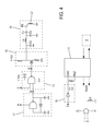
- the cylinder 1 comprises an autonomous power supply (not connected to the mains) such as a battery 6 supplying an electronic read / write circuit 7 (which may be a read-only circuit) and an electronic detection circuit 8.
- the electronic circuit 7 comprises a processing unit 9 for signal processing, authentication of the RFID badge, the authorization or not of mechanical opening of the door.
- This electronic read / write circuit 7 does not communicate with the RFID tag 2 via the respective antennas L1 and L3, only when the detection electronic circuit 8 has detected the presence of the RFID tag 2 which is an electronic identification circuit .
- the two circuits 8 and 9 are said to be independent insofar as each has its own intelligence.
- the diet can be common or not.
- the transmitting antenna can be common and permanently connected to the two circuits 8 and 7 where switched as shown in dotted line on the figure 2 where we see a common antenna L4 alternately connected either to the detection circuit 8 or to the read / write circuit 7 via a switch or switch 10.
- the microcontroller 11 also retrieves the signal supplying the transmitting antenna L2 so as to detect the disturbance due to a mutual coupling with the compatible RFID tag 2.
- the invention is also remarkable in that it makes it possible to discriminate between compatible RFID badge (optimized coupling) and other non-compatible RFID badge (non-optimized coupling).
- the antenna coil L2 can emit an oscillating magnetic field.
- Oscillator 12 is a 13.56MHz oscillator assembly periodically generating very short sinusoidal signal sequences.
- the modulator 13 is a logic circuit adding the signal produced by the oscillator 12 via a resistor R0 (in series) with a control signal coming from the microcontroller 11. This modulator 13 makes it possible to modulate in amplitude the voltage of the oscillator.
- the voltage / current converter 14 makes it possible on the one hand to generate a magnetic field in the antenna L2 by current flow and on the other hand to adjust the level of the current to the lowest to minimize the consumption.
- the antenna coil L2 is integrated within a set 16 said antenna circuit further comprising a resistor Rc and capacitors Cc and C1 whose parameters are determined in agreement with an equivalent antenna circuit of the RFID tag 2 comprising the antenna L3.
- the value of the capacitors is determined so as to eliminate the complex part of the impedance when an RFID tag is in the area of the antenna L2. This thus makes it possible to ensure a magnetic coupling between the antenna L2 and the antenna L3 with a minimum of magnetic field reflection by the RFID tag 2 (electronic identification circuit).
- the assembly is controlled by a micro-controller 11 fast ultra low consumption and having at least a "watchdog” (electronic watchdog) periodic alarm clock, a digital analog converter CAD and a voltage reference if necessary .
- a watchdog electronic watchdog
- the supply voltage Vcc can be monitored by comparing it with the reference voltage directly from the microcontroller. This makes it possible to define different detection levels according to the state of the accumulator.
- the signal from the diode D1 is sent to the digital analog converter CAD of the microcontroller 11.
- the microcontroller will activate the cylinder electronics or not.
- a Capacity discharge cycle is performed systematically before each measurement.
- the capacitance Cn is discharged by setting the corresponding reset connector to zero on the microcontroller 11.
- the time constant RCn is much greater than the processing time of the digital analog converter CAD, or R represents the equivalent resistance of the microcontroller seen by the detection circuit. This makes it possible to minimize the pulse time of the emitted magnetic field and to allow time for the microcontroller to acquire the voltage at the terminals of the antenna even when no field is applied to the antenna .
- the oscillator circuit 17 is different because it integrates in particular a quartz oscillator in parallel of a logic circuit (NAND). Indeed, it is difficult to generate in practice truly sinusoidal signals from a sinusoidal oscillator. It is sometimes preferable to use a periodic signal from a quartz and then filter through a circuit to obtain a high quality sinusoidal signal.
- the modulator 13 is added to the signal produced by the oscillator 17 with a control signal coming from the microcontroller 11.
- the converter 18 makes it possible on the one hand to generate a magnetic field in the antenna L2 by passing current and other to adjust the current level to the lowest to minimize consumption.
- This converter 18 is constituted by a MOS transistor whose gate is connected to the input D, the source to ground via a resistor R1, and the drain to the supply voltage via a coil L5.
- the antenna coil L2 is integrated within a set 13.56 MHz circuit passband said antenna circuit further comprising a coil L6 and capacitors C5, C6 and C7 whose parameters are determined in agreement with an equivalent antenna circuit of the badge RFID 2 comprising the antenna L3.
- the value of the coil L6 and the capacitors is determined so as to eliminate the complex part of the impedance when an RFID tag is in the area of the antenna L2. This thus makes it possible to ensure a magnetic coupling between the antenna L2 and the antenna L3 with a minimum of magnetic field reflection by the RFID tag 2 (electronic identification circuit).
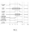
- T1 represents the time required to start the oscillator at 13.56MHz when the supply voltage (oscillator control) is applied to the oscillator 12 of the figure 3 at point A via microcontroller 11 (less than ms).
- Oscillator 12 supplies modulator 13 at point B in a sinusoidal signal.
- a reset of the detection circuit 15 is made by setting the reset state of the microcontroller reset output (on the figure 3 ).
- This pulse is applied to the antenna coil L2 of the detection electronic circuit 8 via the voltage / current converter 14 and the antenna circuit 16 providing an impedance matching (removal of the complex parts).
- the measurement of the voltage detected by the detection circuit 15 is made from the time T3, when the detected voltage no longer varies in amplitude over time and up to the time T4, the time required for the microcontroller to acquire and digital analog processing. This time depends on the clock of the micro controller and is estimated at 10 ⁇ s.
- the detection circuit 15 has a response time close to the micro second.
- the detection signal at the terminals of the antenna L2 is illustrated in E on the figure 4 .
- This signal presents a zone transient between T2 and T3 where it progresses continuously before stabilization.
- the detection signal is illustrated in E 'with a jump of amplitude almost instantaneous T2 and stabilization at a level of amplitude lower than that of the signal detected in the absence of RFID badge.
- the electronic read / write circuit 7 can then communicate with the electronic identification circuit (RFID tag).
- the wake-up signal is sent if the detected level is below a threshold value. Otherwise, no signal is sent, and the microcontroller goes into a "watchdog" state for minimal power consumption and starts a new cycle 300ms later after the To time. To ensure minimum consumption during the state of "watchdog" of the microcontroller 11, it is expected that just before entering the "watchdog” mode, all the legs or connectors of the microcontroller 11 does not have a state to maintain.
- the example described according to the present invention therefore makes it possible to send periodically (typically every 300 ms) a current pulse in the coupling coil, via a network tuned to 13.56 MHz, and then to measure the waveform of the attenuation of the oscillation signal on this coil.
- the level of attenuation allows to validate or not the presence of an RFID badge.
Landscapes
- Engineering & Computer Science (AREA)
- Artificial Intelligence (AREA)
- Computer Vision & Pattern Recognition (AREA)
- Physics & Mathematics (AREA)
- General Physics & Mathematics (AREA)
- Theoretical Computer Science (AREA)
- Near-Field Transmission Systems (AREA)
Abstract
Description
La présente invention concerne un procédé de communication radiofréquence comprenant un circuit électronique de lecture/écriture destiné à communiquer à distance avec un circuit électronique d'identification tel un badge RFID (Radio Fréquences Identification). Il est également prévu un système pour mettre en oeuvre un tel procédé. Par circuit électronique de lecture/écriture, on entend un circuit électronique de lecture et/ou d'écriture.The present invention relates to a radiofrequency communication method comprising an electronic read / write circuit for communicating remotely with an electronic identification circuit such as an RFID (Radio Frequency Identification) badge. There is also provided a system for implementing such a method. By read / write electronic circuit is meant an electronic circuit for reading and / or writing.
L'invention trouve une application particulièrement intéressante dans le domaine de contrôle d'accès sans contact mais peut avantageusement s'appliquer à tout système de communication comprenant un lecteur et un badge sans contact.The invention finds a particularly interesting application in the field of contactless access control but can advantageously be applied to any communication system comprising a reader and a contactless badge.
Plus particulièrement, l'invention concerne le domaine des circuits de veille actifs utilisant la technologie de détection par couplage magnétique en champ proche, notamment pour une communication RFID à 13.56 MHz selon la norme ISO 14443 par exemple.More particularly, the invention relates to the field of active watch circuits using magnetic field detection technology in the near field, in particular for a 13.56 MHz RFID communication according to ISO 14443 for example.
Concernant les circuits de veille actifs, différentes technologies peuvent êtres utilisées :
- Réveil de façon cyclique du circuit électronique du lecteur avec tentative systématique de lecture/écriture de badges. Cette méthode de détection/identification de moyens d'identification sans contact nécessite une consommation de courant instantanée non négligeable par le lecteur pour l'émission du champ magnétique et la lecture ou tentative de lecture ou autre élément permettant d'identifier la présence d'un média d'identification. Cette solution n'est pas envisageable dans des systèmes embarqués compte tenu des consommations de courant, conduisant à une durée de vie de la pile estimée à quelques jours tout au plus.
- Circuit à variation de capacité : cette solution dépend beaucoup de l'environnement (matériaux du support cylindre, du sol, etc...) rendant sa mise en oeuvre délicate.
- Système utilisant un émetteur récepteur infrarouge. Lorsqu'un média d'identification se trouve dans le champ de rayonnement infrarouge, le lecteur détecte et bascule l'électronique du cylindre en mode actif, où émet un champ magnétique pour établir une communication avec le média d'identification. Cette solution ne permet pas de détecter de façon certaine la présence d'un média d'identification mais détecte tout objet ou autre qui réfléchit le signal infrarouge sur le détecteur infrarouge. Cette méthode de veille conduit à utiliser plus du tiers de l'énergie disponible rien que pour la veille, conduisant à une espérance d'autonomie voisine de 2,5 ans pour une utilisation de 50 cycles ouverture/fermeture quotidiens.
- Cyclic awakening of the electronic circuit of the reader with systematic attempt to read / write badges. This method of detecting / identifying non-contact identification means requires a considerable instantaneous current consumption by the reader for the emission of the magnetic field and the reading or reading attempt or other element making it possible to identify the presence of a identification media. This solution is not possible in embedded systems considering power consumption, leading to a battery life estimated at a few days at most.
- Circuit with capacity variation: this solution depends a lot on the environment (materials of the cylinder support, the ground, etc ...) making its implementation delicate.
- System using an infrared transceiver. When an identification medium is in the infrared radiation field, the reader detects and switches the electronics of the cylinder into active mode, where a magnetic field emits to establish communication with the media Identification. This solution does not detect with certainty the presence of identification media but detects any object or other that reflects the infrared signal on the infrared detector. This method of monitoring leads to using more than a third of the available energy just for the day before, leading to an expected autonomy of 2.5 years for a use of 50 cycles opening / closing daily.
On connaît le document
On connaît le document
On connaît également le document
L'inconvénient de ces dispositifs est que le circuit de veille obéit souvent à un protocole propriétaire qui est fonction du circuit électronique de lecture/écriture.The disadvantage of these devices is that the watch circuit often obeys a proprietary protocol which is a function of the electronic read / write circuit.
La présente invention a pour but un nouveau système de veille économe en énergie. Un autre but de l'invention est de prévoir une adaptation simple avec différents protocoles ou standards de communication radiofréquence entre un lecteur et un badge radiofréquence.The object of the present invention is to provide a new energy saving watch system. Another object of the invention is to provide a simple adaptation with different protocols or radio frequency communication standards between a reader and a radiofrequency badge.
On atteint au moins l'un des objectifs avec un procédé de communication radiofréquence comprenant un circuit électronique de lecture/écriture destiné à communiquer à distance avec un circuit électronique d'identification. Selon l'invention, le circuit électronique de lecture/écriture étant en mode de veille ou éteint :
- on utilise un circuit électronique de détection, indépendant du circuit électronique de lecture/écriture, pour générer de façon répétitive un signal d'excitation adapté à la résonance d'un circuit antenne au sein de ce circuit électronique de détection et adapté pour engendrer un phénomène de résonance dans un circuit antenne du circuit électronique d'identification lorsque ce dernier se trouve à la portée du circuit électronique de détection,
- on réalise une analyse de couplage inductif résonant à partir de l'amplitude d'un signal prélevé sur le circuit antenne du circuit électronique de détection,
- en cas de détection de la présence d'un circuit électronique d'identification, on active le circuit électronique de lecture/écriture de façon à permettre la communication entre ce circuit électronique de lecture/écriture et le circuit électronique d'identification.
- an electronic detection circuit, independent of the electronic read / write circuit, is used to repetitively generate an excitation signal adapted to the resonance of an antenna circuit within this electronic detection circuit and adapted to generate a phenomenon resonance in an antenna circuit of the electronic identification circuit when the latter is within range of the electronic detection circuit,
- an inductive resonant coupling analysis is carried out on the basis of the amplitude of a signal taken from the antenna circuit of the electronic detection circuit,
- in case of detection of the presence of an electronic identification circuit, activates the electronic read / write circuit so as to allow communication between the electronic read / write circuit and the electronic identification circuit.
Le procédé selon l'invention permet donc de détecter la présence d'un circuit électronique d'identification ou tout moyen d'authentification sans contact tel un badge RFID, dans la zone de communication d'un lecteur sans message d'identification.The method according to the invention thus makes it possible to detect the presence of an electronic identification circuit or any contactless authentication means such as an RFID badge, in the communication zone of a reader without an identification message.
Par le caractère indépendant du circuit électronique de détection par rapport au circuit électronique de lecture/écriture, on entend une indépendance de l'électronique, c'est-à-dire de l'intelligence, de l'unité de traitement. L'unité de traitement telle un microprocesseur ou microcontrôleur gérant le circuit électronique de lecture/écriture n'est pas le même que celui gérant le circuit électronique de détection même s'il existe bien sûr une communication entre les deux circuits électroniques. Le circuit électronique de détection ne sert qu'à détecter la présence d'un moyen d'authentification sans pratiquer l'authentification proprement parlée et à mettre le circuit électronique de lecture/écriture en mode actif lorsqu'un moyen d'authentification est détecté.By the independent nature of the electronic detection circuit with respect to the electronic read / write circuit means an independence of the electronics, that is to say, the intelligence of the processing unit. The processing unit such as a microprocessor or microcontroller managing the electronic read / write circuit is not the same as that managing the electronic detection circuit even if there is of course a communication between the two electronic circuits. The electronic detection circuit serves only to detect the presence of an authentication means without practicing proper authentication and to put the electronic read / write circuit in active mode when an authentication means is detected.
La présente invention apporte une véritable solution aux inconvénients de l'art antérieur. D'une part, l'invention peut être intégrée dans tout système fonctionnant par couplage magnétique, quelque soit la norme, le protocole de communication la fréquence de la porteuse et laisse un choix sans limite à l'homme du métier dans le choix des circuits ou composants au moment de la conception. D'autre part dans son mode de fonctionnement, la détection ne se fait pas par comparaison avec un signal de référence issu et prélevé des impulsions précédentes comme dans l'art antérieur, mais sur la mesure absolue de la valeur de ce signal avec de préférence une remise à zéro du circuit de détection avant chaque mesure.The present invention provides a real solution to the disadvantages of the prior art. On the one hand, the invention can be integrated into any system operating by magnetic coupling, whatever the standard, the communication protocol the frequency of the carrier and leaves a limitless choice to those skilled in the choice of circuits or components at the time of design. On the other hand, in its mode of operation, the detection is not made by comparison with a reference signal derived from and taken from previous pulses as in the prior art, but on the absolute measurement of the value of this signal, preferably a reset of the detection circuit before each measurement.
De préférence, le circuit antenne du circuit électronique de détection comprend un circuit RLC (résistance-bobine-condensateur) dans lequel la bobine sert d'antenne d'émission. En pratique, pour que le circuit de détection soit bien adapté, on rajoute de préférence une self ou bobine en plus de l'antenne. Généralement, l'antenne est gravée sur un circuit imprimé et sa valeur n'est pas facilement ajustable. Les moyens de réception dans le circuit électronique d'identification peuvent être équivalents à un circuit RLC. Le couplage magnétique a lieu entre les bobines. On peut par ailleurs prévoir un mode de réalisation où le circuit électronique de détection et le circuit électronique de lecture/écriture partagent une même antenne qui est connectée d'une part au circuit de veille et d'autre part au circuit de lecture/écriture du circuit principal. Cette solution est utilisée lorsque le circuit de veille et le circuit de lecture/écriture ne se perturbent pas mutuellement. Si tel était le cas (perturbation mutuelle), alors il suffirait d'utiliser un switch permettant de raccorder l'unité de traitement de l'un puis l'autre circuit.Preferably, the antenna circuit of the electronic detection circuit comprises an RLC circuit (coil-capacitor-capacitor) in which the coil serves as a transmitting antenna. In practice, for the detection circuit to be well adapted, it is preferable to add a coil or coil in addition to the antenna. Generally, the antenna is engraved on a circuit board and its value is not easily adjustable. The receiving means in the electronic identification circuit may be equivalent to an RLC circuit. The magnetic coupling takes place between the coils. An embodiment may also be provided in which the electronic detection circuit and the electronic read / write circuit share a same antenna which is connected on the one hand to the idle circuit and on the other hand to the read / write circuit of the main circuit. This solution is used when the standby circuit and the read / write circuit do not disturb each other. If this were the case (mutual disruption), then it would be enough to use a switch to connect the processing unit of one then the other circuit.
Selon une caractéristique avantageuse de l'invention, on alimente le circuit électronique de lecture/écriture et le circuit électronique de détection au moyen d'une batterie, pile ou accumulateur. Les deux circuits électroniques de détection et de lecture/écriture peuvent être alimentés par une même batterie et par des batteries différentes. Il s'agit donc d'une alimentation autonome, c'est-à-dire non connectée à une source d'énergie extérieure. La batterie à une durée de vie qui dépend principalement de l'énergie consommée. Il est donc nécessaire que le circuit électronique de lecture/écriture ne soit actif que lorsqu'un circuit électronique d'identification ou moyen d'authentification se trouve dans la zone de communication de son antenne.According to an advantageous characteristic of the invention, the electronic read / write circuit and the electronic detection circuit are fed by means of a battery, battery or accumulator. The two electronic detection and read / write circuits can be powered by the same battery and by different batteries. It is therefore an autonomous power supply, that is to say not connected to an external power source. The battery has a lifetime that depends mainly on the energy consumed. It is therefore necessary for the electronic read / write circuit to be active only when an electronic identification circuit or authentication means is in the communication zone of its antenna.
A la lecture de ce qui précède, il est donc important de minimiser la consommation de courant, en particulier en minimisant au maximum le courant traversant la bobine antenne du circuit électronique de détection. Pour pouvoir discriminer efficacement, à partir d'un courant faible, l'amplitude d'un signal correspondant à la présence du circuit électronique d'identification, la présente invention prévoit un fort couplage magnétique (inductif) entre la bobine du circuit électronique de détection et celle du circuit électronique d'identification. Pour ce faire, on prévoit un couplage inductif résonant. A la résonance, l'intensité du courant augmente et passe par un maximum. S'il n'y a aucun couplage, l'amplitude du signal circulant dans la bobine du circuit électronique de détection sera forte. S'il y a couplage en présence d'un circuit antenne dans un circuit électronique d'identification proche, alors l'amplitude du signal dans la bobine du circuit électronique de détection sera autant diminuée que le couplage sera fort. Pour que la variation d'amplitude du signal avec couplage et sans couplage soit significative, on prévoit un couplage fort en réalisant un couplage inductif résonant en présence d'un circuit électronique d'identification adapté.On reading the above, it is therefore important to minimize the current consumption, in particular by minimizing as much as possible the current flowing through the antenna coil of the electronic detection circuit. In order to effectively discriminate, from a low current, the amplitude of a signal corresponding to the presence of the electronic identification circuit, the present invention provides a strong magnetic coupling (inductive) between the coil of the electronic detection circuit. and that of the electronic identification circuit. To do this, an inductive resonant coupling is provided. At resonance, the intensity of the current increases and goes through a maximum. If there is no coupling, the amplitude of the signal flowing in the coil of the electronic detection circuit will be strong. If there is coupling in the presence of an antenna circuit in a near identification electronic circuit, then the amplitude of the signal in the coil of the electronic detection circuit will be reduced as much as the coupling will be strong. In order for the amplitude variation of the signal with coupling and without coupling to be significant, a strong coupling is provided by performing an inductive resonant coupling in the presence of a suitable electronic identification circuit.
Techniquement, on obtient ce fort couplage, lorsque les impédances du circuit électronique de détection et du circuit électronique d'identification sont adaptées de façon à obtenir une impédance réelle en annulant la composante complexe des circuits. Si ces impédances sont mal adaptées, la majorité du champ magnétique serait réfléchie par le circuit électronique d'identification et non transmise, ce qui diminuerait le couplage magnétique entre la bobine du circuit électronique de détection et celle du circuit électronique d'identification, et qui ne permettrait pas une détection à faible courant.Technically, this strong coupling is obtained when the impedances of the electronic detection circuit and the electronic identification circuit are adapted so as to obtain a real impedance by canceling the complex component of the circuits. If these impedances are poorly adapted, the majority of the magnetic field would be reflected by the electronic identification circuit and not transmitted, which would reduce the magnetic coupling between the coil of the electronic detection circuit and that of the electronic identification circuit, and would not allow a low current detection.
En d'autres termes, lorsqu'un circuit électronique d'identification sans contact se trouve dans la zone de communication du circuit électronique de détection qui comporte une bobine d'antenne, l'amplitude du champ magnétique émis par le circuit électronique de détection se trouve altéré, la bobine du circuit électronique d'identification interfère avec la bobine antenne d'émission par couplage inductif, ce qui désaccorde sensiblement le circuit d'émission (circuit électronique de détection). Ainsi, il suffit de surveiller l'amplitude du champ magnétique aux bornes de la bobine antenne du circuit électronique de détection.In other words, when a non-contact electronic identification circuit is in the communication zone of the detection electronic circuit which comprises an antenna coil, the amplitude of the magnetic field emitted by the electronic detection circuit is is altered, the coil of the electronic identification circuit interferes with the inductive coupling emission antenna coil, which substantially disconnects the transmission circuit (electronic detection circuit). Thus, it suffices to monitor the amplitude of the magnetic field at the terminals of the antenna coil of the electronic detection circuit.
Selon une caractéristique avantageuse de l'invention, on génère le signal d'excitation de façon cyclique ou périodique, le cycle de génération étant notamment inférieur à 1seconde, de préférence comprise entre 250ms et 400ms. D'autre part, selon l'invention, il suffit d'émettre des impulsions de champ magnétique de très courte durée, n'entrainant qu'une faible consommation de courant et de surveiller par un circuit de détection rapide l'amplitude du signal aux bornes de la bobine antenne du circuit électronique de détection. La récurrence de cette impulsion donne le cycle de veille. Pour des applications liées à l'ouverture d'une porte après authentification d'un badge RFID par exemple, si on estime le temps d'authentification et de traitement d'une ouverture à 600 ms, temps nécessaire dans le cas d'un échange sécurisé, et en acceptant un temps d'attente entre la présentation d'un badge RFID et l'ouverture du cylindre inférieur à une seconde, le temps entre deux impulsions magnétiques successives est de préférence inférieur à 400 ms, idéalement égale ou proche de 300ms.According to an advantageous characteristic of the invention, the excitation signal is generated cyclically or periodically, the generation cycle being in particular less than 1second, preferably between 250ms and 400ms. On the other hand, according to the invention, it is sufficient to emit magnetic field pulses of very short duration, resulting in only a small current consumption and to monitor by a fast detection circuit the amplitude of the signal at the same time. terminals of the antenna coil of the electronic detection circuit. The recurrence of this pulse gives the watch cycle. For applications related to the opening of a door after authentication of an RFID badge, for example, if the authentication and processing time of an opening is estimated at 600 ms, time required in the case of an exchange secure, and accepting a waiting time between the presentation of an RFID badge and the opening of the lower cylinder to one second, the time between two successive magnetic pulses is preferably less than 400 ms, ideally equal to or close to 300 ms .
Selon un mode de mise en oeuvre de l'invention, l'analyse de couplage inductif résonant comprend la mesure du niveau de l'amplitude d'un signal passant par la bobine du circuit électronique de détection, notamment pendant le couplage magnétique entre les deux circuits antennes lorsque ce dernier se trouve à la portée du circuit électronique de détection. En mode de fonctionnement, il est préférable de laisser passer un certain temps avant de réaliser la mesure d'amplitude.According to one embodiment of the invention, the resonant inductive coupling analysis comprises measuring the amplitude level of a signal passing through the coil of the electronic detection circuit, in particular during the magnetic coupling between the two antenna circuits when the latter is within range of the electronic detection circuit. In the operating mode, it is best to allow some time to complete the amplitude measurement.
La détection de l'amplitude sur la bobine peut se faire en chargeant un condensateur connecté à la bobine via une diode, ce condensateur étant complètement déchargé avant chaque détection.Detection of the amplitude on the coil can be done by charging a capacitor connected to the coil via a diode, this capacitor being completely discharged before each detection.
De préférence, on active le circuit électronique de lecture/écriture lorsque l'amplitude mesurée sur la bobine servant d'antenne dans le circuit électronique de détection est inférieure à un seuil donné, ce seuil étant fonction de la tension d'alimentation du circuit électronique de détection.Preferably, the electronic read / write circuit is activated when the amplitude measured on the coil acting as antenna in the electronic detection circuit is less than a given threshold, this threshold being a function of the supply voltage of the electronic circuit. detection.
Avantageusement, le signal d'excitation émis est un signal périodique, de faible intensité, à la fréquence de résonance du circuit antenne du circuit électronique d'identification.Advantageously, the emitted excitation signal is a periodic signal, of low intensity, at the resonant frequency of the antenna circuit of the electronic identification circuit.
Afin de limiter au maximum la consommation, on peut placer le circuit électronique de détection en mode ultra basse consommation entre deux émissions du signal d'excitation.In order to limit the consumption as much as possible, the detection electronic circuit can be placed in ultra-low power mode between two transmissions of the excitation signal.
Selon un autre aspect de l'invention, il est proposé un système de communication radiofréquence comprenant un circuit électronique de lecture/écriture destiné à communiquer à distance avec un circuit électronique d'identification. Le système selon l'invention comprend en outre :
- un circuit électronique de détection, indépendant du circuit électronique de lecture/écriture, pour générer de façon répétitive un signal d'excitation adapté à la résonance d'un circuit antenne au sein de ce circuit électronique de détection et adapté pour engendrer un phénomène de résonance dans un circuit antenne du circuit électronique d'identification lorsque ce dernier se trouve à la portée du circuit électronique de détection,
- une unité de traitement au sein du circuit électronique de détection pour réaliser une analyse de couplage inductif résonant à partir de l'amplitude d'un signal prélevé sur le circuit antenne du circuit électronique de détection, et pour activer le circuit électronique de lecture/écriture de façon à permettre la communication entre ce circuit électronique de lecture/écriture et le circuit électronique d'identification en cas de détection de la présence de ce circuit électronique d'identification.
- an electronic detection circuit, independent of the electronic read / write circuit, for repetitively generating an excitation signal adapted to the resonance of an antenna circuit within this electronic detection circuit and adapted to generate a resonance phenomenon in an antenna circuit of the electronic identification circuit when the latter is within range of the electronic detection circuit,
- a processing unit within the electronic detection circuit for performing a resonant inductive coupling analysis from the amplitude of a signal taken from the antenna circuit of the electronic detection circuit, and to activate the electronic read / write circuit so as to allow communication between this electronic read / write circuit and the electronic identification circuit in case of detection of the presence of this electronic identification circuit.
Avantageusement, le système selon l'invention peut comprendre en outre un cylindre de porte dans lequel sont disposés :
- le circuit électronique de lecture/écriture ;
- le circuit électronique de détection ; et
- une batterie d'alimentation.
- the electronic read / write circuit;
- the electronic detection circuit; and
- a battery pack.
L'invention peut donc concerner un système de veille actif qui détecte la présente d'un badge RFID présent dans la zone de communication de l'antenne d'un cylindre électronique autonome alimenté par un accumulateur. Ce cylindre électronique est destiné à être monté sur une porte ou tout autre support et est destiné à faire du contrôle d'accès à partir de la lecture/écriture de circuits intégrés sans contact ou supports d'authentifications ou média d'identification présentés dans le champ de communication du lecteur du cylindre en utilisant la technologie RFID notamment.The invention can therefore relate to an active standby system which detects the presence of an RFID badge present in the communication zone of the antenna of an autonomous electronic cylinder powered by an accumulator. This electronic cylinder is intended to be mounted on a door or other support and is intended to make access control from the read / write of contactless integrated circuits or authentication media or identification media presented in FIG. communication field of the cylinder reader using RFID technology in particular.
Selon un mode de réalisation préféré, le circuit électronique de détection peut comprendre un oscillateur, un modulateur, un convertisseur tension/courant et un microcontrôleur pour :
- commander l'émission du signal d'excitation,
- analyser le couplage inductif résonant après détection de l'amplitude sur la bobine, et
- activer le circuit électronique de lecture/écriture en cas de détection de la présence d'un circuit électronique d'identification.
- control the emission of the excitation signal,
- analyze the resonant inductive coupling after detection of the amplitude on the coil, and
- activate the electronic read / write circuit in case of detection of the presence of an electronic identification circuit.
Pour assurer une grande autonomie dans le temps du cylindre électronique autonome alimenté par un accumulateur, la consommation de l'ensemble de l'électronique du cylindre peut être minimisée en se mettant dans un mode veille actif lorsque le cylindre n'a pas besoin d'opérer de transactions (échanges de données, interrogation d'autorisations d'ouverture etc), mais doit être actif et donc alimenté lorsqu'un moyen d'identification est dans la zone de communication de l'antenne du cylindre.To ensure a long autonomy in the time of the autonomous electronic cylinder powered by an accumulator, the consumption of all the electronics of the cylinder can be minimized by putting itself in an active standby mode when the cylinder does not need to operate transactions (data exchange, opening authorization interrogation etc.), but must be active and therefore powered when an identification means is in the communication area of the cylinder antenna.
Par ailleurs, le circuit électronique de détection peut comprendre en outre un circuit de détection d'amplitude disposé entre la bobine et une entrée du microcontrôleur et comprenant :
- une diode dont l'anode est connectée à la bobine et la cathode au microcontrôleur, et
- un condensateur disposé entre la cathode de la diode et la masse.
- a diode whose anode is connected to the coil and the cathode to the microcontroller, and
- a capacitor disposed between the cathode of the diode and the ground.
D'autres avantages et caractéristiques de l'invention apparaîtront à l'examen de la description détaillée d'un mode de mise en oeuvre nullement limitatif, et des dessins annexés, sur lesquels :
- La
figure 1 est une vue simplifiée d'un cylindre de porte pour la mise en oeuvre de la présente invention ; - La
figure 2 est un schéma électronique simplifié d'un système de communication sans contact selon l'invention ; - La
figure 3 est une vue plus détaillée du système de lafigure 2 ; - La
figure 4 est une variante du système de lafigure 3 ; et - La
figure 5 est une vue illustrant le cycle temporel des différents signaux à travers le système de communication selon l'invention.
- The
figure 1 is a simplified view of a door cylinder for carrying out the present invention; - The
figure 2 is a simplified circuit diagram of a contactless communication system according to the invention; - The
figure 3 is a more detailed view of the system of thefigure 2 ; - The
figure 4 is a variant of the system of thefigure 3 ; and - The
figure 5 is a view illustrating the time cycle of the various signals through the communication system according to the invention.
Bien que l'invention n'y soit pas limitée, on va maintenant décrire le procédé et le système selon l'invention appliqués à un cylindre pour le contrôle d'accès d'une porte.Although the invention is not limited thereto, the method and system according to the invention applied to a cylinder for access control of a door will now be described.
On notera que l'invention peut également s'appliquer à tout système de communication sans contact par couplage magnétique dans lequel on souhaite ou non limiter au maximum la consommation d'énergie, en particulier dans des systèmes embarqués.It should be noted that the invention can also be applied to any contactless communication system by magnetic coupling in which one whether or not to limit energy consumption as much as possible, especially in embedded systems.
Sur la
Sur la
Le circuit électronique de détection 8 comprend un micro contrôleur 11 contrôlant :
un oscillateur 12 apte à générer un signal d'excitation qui est sinusoïdal de très courte durée,un modulateur 13 pour délimiter convenablement la durée du signal d'excitation, et- un convertisseur tension/
courant 14 pour alimenter l'antenne d'émission L2.
- an
oscillator 12 capable of generating an excitation signal which is sinusoidal of very short duration, - a
modulator 13 for suitably delimiting the duration of the excitation signal, and - a voltage /
current converter 14 for supplying the transmitting antenna L2.
Le micro contrôleur 11 récupère également le signal alimentant l'antenne d'émission L2 de façon à détecter la perturbation due à un couplage mutuel avec le badge RFID 2 compatible.The
L'invention est aussi remarquable par le fait qu'elle permet de discriminer entre badge RFID compatible (couplage optimisé) et autre badge RFID non compatible (couplage non optimisé).The invention is also remarkable in that it makes it possible to discriminate between compatible RFID badge (optimized coupling) and other non-compatible RFID badge (non-optimized coupling).
Sur la
On distingue également un détecteur 15 pour détecter la variation de niveau du champ magnétique aux bornes de la bobine antenne L2 du circuit interrogateur lorsqu'un média d'identification est dans la zone de communication de la bobine antenne L2. Le circuit de détection 15 est constitué par une diode Schottky rapide D1 et d'une capacité Cn (non représentés sur la
Toujours pour minimiser la consommation de courant, le circuit 8 passe en mode inactif lorsqu'aucun champ magnétique n'est envoyé à l'antenne. Il est évident, pour l'homme du métier que ce circuit 8 peut être réalisé de façon différente. Le système est performant lorsqu'on applique à la bobine antenne du circuit électronique 8 des impulsions d'oscillations à la fréquence d'accord des circuits antennes comprenant respectivement L2 et L3, de courtes durées avec une amplitude minimale exploitable par le circuit électronique de détection.Always to minimize the current consumption, the
L'ensemble est piloté par un micro contrôleur 11 rapide ultra basse consommation et disposant à minima d'un « watchdog » (chien de garde électronique) de réveil périodique, d'un convertisseur analogique numérique CAD et d'une référence de tension si nécessaire.The assembly is controlled by a
Ce micro contrôleur 11 pilote le circuit 8 pour :
- la mise en route de l'oscillateur 12,
- la décharge de la capacité de détection Cn, et
- L'envoi du signal de modulation sur le modulateur 13.
- the startup of the
oscillator 12, - the discharge of the detection capacitance Cn, and
- The sending of the modulation signal on the
modulator 13.
La tension d'alimentation Vcc peut être surveillée en la comparant à la tension de référence directement issue du micro contrôleur. Cela permet de définir des niveaux de détection différents suivant l'état de l'accumulateur.The supply voltage Vcc can be monitored by comparing it with the reference voltage directly from the microcontroller. This makes it possible to define different detection levels according to the state of the accumulator.
Lors de la détection, le signal provenant de la diode D1 est envoyé sur le convertisseur analogique numérique CAD du micro contrôleur 11. Suivant la valeur de la tension détectée, le micro contrôleur activera ou non l'électronique du cylindre.During the detection, the signal from the diode D1 is sent to the digital analog converter CAD of the
Pour s'assurer qu'à chaque cycle de mesure, le niveau détecté par la diode D1 et Cn ne soit perturbée par les mesures précédentes, c'est-à-dire qu'une tension résiduelle subsiste aux bornes de la capacité Cn, un cycle de décharge de la capacité est réalisé de façon systématique avant chaque mesure. Ainsi, avant chaque détection, la capacité Cn est déchargée par la mise à zéro du connecteur RAZ correspondant sur le micro contrôleur 11.To ensure that at each measurement cycle, the level detected by the diode D1 and Cn is disturbed by the preceding measurements, that is to say that a residual voltage remains across the capacitance Cn, a Capacity discharge cycle is performed systematically before each measurement. Thus, before each detection, the capacitance Cn is discharged by setting the corresponding reset connector to zero on the
Concernant la valeur de la capacité Cn, elle est définie pour que la constante de temps RCn soit très supérieure au temps de traitement du convertisseur analogique numérique CAD, ou R représente la résistance équivalente du micro contrôleur vue par le circuit de détection. Cela permet de minimiser le temps de l'impulsion du champ magnétique émis et de laisser le temps au micro contrôleur d'effectuer l'acquisition de la tension aux bornes de l'antenne même lorsqu'aucun champ n'est appliqué sur l'antenne.Concerning the value of the capacitance Cn, it is defined so that the time constant RCn is much greater than the processing time of the digital analog converter CAD, or R represents the equivalent resistance of the microcontroller seen by the detection circuit. This makes it possible to minimize the pulse time of the emitted magnetic field and to allow time for the microcontroller to acquire the voltage at the terminals of the antenna even when no field is applied to the antenna .
Les sorties G et H du microcontrôleur 11 peuvent être utilisées par un switch lorsqu'on utilise une seule antenne L4 par exemple à la place des deux antennes L1 et L2. Ce switch est représenté schématiquement en pointillé sur la figue 3. L'entrée I serait reliée à un modulateur/démodulateur du circuit 9. L'entrée E est l'entrée du circuit de détection. Les entrées G et H sont des commandes permettant de sélectionner soit l'entrée I soit l'entrée E pour une connexion avec l'antenne unique L4.The outputs G and H of the
Sur la
Sur la
To est l'origine des temps du début d'un cycle de détection de circuit électronique d'identification ou badge RFID. T1 représente le temps nécessaire à la mise en route de l'oscillateur à 13.56MHz lorsque la tension d'alimentation (commande oscillateur) est appliquée à l'oscillateur 12 de la
Au temps To de mise en route de l'oscillateur à 13.56MHz, une RAZ du circuit de détection 15 est opérée par la mise à l'état bas de la sortie RAZ du micro contrôleur (sur la
Au temps T2, supérieur au temps T1, la sortie RAZ du micro contrôleur 11 est en haute impédance (niveau libre) et le micro contrôleur envoie au modulateur 13 un pulse voisin de 2µs au point C. En sortie D du modulateur 13, on obtient un signal sinusoïdal de durée identique à la durée du pulse appliqué au point C.At time T2, which is greater than time T1, the reset output of
Cette impulsion est appliquée à la bobine d'antenne L2 du circuit électronique de détection 8 par l'intermédiaire du convertisseur tension/courant 14 et du circuit antenne 16 réalisant une adaptation d'impédance (suppression des parties complexes).This pulse is applied to the antenna coil L2 of the detection
La mesure de la tension détectée par le circuit de détection 15 est faite à partir du temps T3, moment où la tension détectée ne varie plus en amplitude dans le temps et jusqu'au temps T4, temps nécessaire au micro contrôleur de faire l'acquisition et le traitement analogique numérique. Ce temps dépend de l'horloge du micro contrôleur et est estimé à 10µs. Le circuit de détection 15 a un temps de réponse voisin de la micro seconde.The measurement of the voltage detected by the
Ensuite, suivant la valeur du signal détectée, un signal peut être envoyé vers le circuit électronique de lecture/écriture 7 (unité de traitement 9) par le micro contrôleur pour réveil.Then, depending on the value of the detected signal, a signal can be sent to the read / write electronic circuit 7 (processing unit 9) by the wake-up microcontroller.
En absence de badge RFID, le signal de détection aux bornes de l'antenne L2 est illustré en E sur la
En présence de badge RFID, le signal de détection est illustré en E' avec un saut d'amplitude quasi instantané en T2 puis stabilisation à un niveau d'amplitude inférieur à celui du signal détecté en absence de badge RFID. Le circuit électronique de lecture/écriture 7 peut ensuite communiquer avec le circuit électronique d'identification (badge RFID). Le signal de réveil est envoyé si le niveau détecté est inférieur à une valeur seuil. Dans le cas contraire, aucun signal n'est envoyé, et le micro contrôleur se met en état de « watchdog » pour une consommation minimale et recommence un nouveau cycle 300ms plus tard après le temps To. Pour garantir une consommation minimale pendant l'état de « watchdog » du micro contrôleur 11, on prévoit que juste avant l'entrée en mode « watchdog », l'ensemble des pattes ou connecteurs du micro contrôleur 11 n'ait pas un état à maintenir.In the presence of RFID badge, the detection signal is illustrated in E 'with a jump of amplitude almost instantaneous T2 and stabilization at a level of amplitude lower than that of the signal detected in the absence of RFID badge. The electronic read /
Lorsqu'un badge RFID est dans la zone de communication de la bobine antenne L2, un dialogue peut s'opérer entre le micro contrôleur 11 et le circuit électronique de lecture/écriture. Ainsi, dès la détection d'un badge RFID, un signal peut être envoyé vers le circuit électronique de lecture/écriture 7. Le micro contrôleur 11 du circuit électronique de détection peut ensuite attendre une information de l'électronique du cylindre pour redémarrer son cycle de détection de média d'identification tous les 300ms.When an RFID tag is in the communication zone of the antenna coil L2, a dialogue can take place between the
L'exemple décrit selon la présente invention permet donc d'envoyer périodiquement (typiquement toutes les 300ms) une impulsion de courant dans la bobine de couplage, via un réseau accordé à 13,56MHz, puis de mesurer la forme d'onde de l'atténuation du signal d'oscillation sur cette bobine. Le niveau de l'atténuation permet de valider ou non la présence d'un badge RFID.The example described according to the present invention therefore makes it possible to send periodically (typically every 300 ms) a current pulse in the coupling coil, via a network tuned to 13.56 MHz, and then to measure the waveform of the attenuation of the oscillation signal on this coil. The level of attenuation allows to validate or not the presence of an RFID badge.
Bien sûr, l'invention n'est pas limitée aux exemples qui viennent d'être décrits et de nombreux aménagements peuvent être apportés à ces exemples sans sortir du cadre de l'invention.Of course, the invention is not limited to the examples that have just been described and many adjustments can be made to these examples without departing from the scope of the invention.
Claims (15)
Priority Applications (1)
| Application Number | Priority Date | Filing Date | Title |
|---|---|---|---|
| EP11305350A EP2506185A1 (en) | 2011-03-29 | 2011-03-29 | Radiofrequency communication method with detection of the presence of an RFID chip and system implementing such a method. |
Applications Claiming Priority (1)
| Application Number | Priority Date | Filing Date | Title |
|---|---|---|---|
| EP11305350A EP2506185A1 (en) | 2011-03-29 | 2011-03-29 | Radiofrequency communication method with detection of the presence of an RFID chip and system implementing such a method. |
Publications (1)
| Publication Number | Publication Date |
|---|---|
| EP2506185A1 true EP2506185A1 (en) | 2012-10-03 |
Family
ID=44510065
Family Applications (1)
| Application Number | Title | Priority Date | Filing Date |
|---|---|---|---|
| EP11305350A Withdrawn EP2506185A1 (en) | 2011-03-29 | 2011-03-29 | Radiofrequency communication method with detection of the presence of an RFID chip and system implementing such a method. |
Country Status (1)
| Country | Link |
|---|---|
| EP (1) | EP2506185A1 (en) |
Citations (5)
| Publication number | Priority date | Publication date | Assignee | Title |
|---|---|---|---|---|
| EP0966112A1 (en) | 1998-06-18 | 1999-12-22 | Sgs Thomson Microelectronics Sa | Method and system for inductive coupling detection of a charge modulation signal |
| EP1148437A2 (en) * | 2000-04-20 | 2001-10-24 | Carl H . Scheuermann | Identification system |
| FR2833785A1 (en) | 2001-12-18 | 2003-06-20 | Inside Technologies | Electronic tag/badge inductive coupling transmission having short duration pulses magnetic field transmitted and pulse envelope integrated circuit returned/extracted with detector finding amplitude variation near integrated circuit. |
| US20070188326A1 (en) | 2004-03-03 | 2007-08-16 | Marcel Pluss | Method for recognizing identification media |
| WO2009018790A1 (en) * | 2007-08-08 | 2009-02-12 | Comimfo, A.S. | Equipment for contactless integrated circuit reading |
-
2011
- 2011-03-29 EP EP11305350A patent/EP2506185A1/en not_active Withdrawn
Patent Citations (5)
| Publication number | Priority date | Publication date | Assignee | Title |
|---|---|---|---|---|
| EP0966112A1 (en) | 1998-06-18 | 1999-12-22 | Sgs Thomson Microelectronics Sa | Method and system for inductive coupling detection of a charge modulation signal |
| EP1148437A2 (en) * | 2000-04-20 | 2001-10-24 | Carl H . Scheuermann | Identification system |
| FR2833785A1 (en) | 2001-12-18 | 2003-06-20 | Inside Technologies | Electronic tag/badge inductive coupling transmission having short duration pulses magnetic field transmitted and pulse envelope integrated circuit returned/extracted with detector finding amplitude variation near integrated circuit. |
| US20070188326A1 (en) | 2004-03-03 | 2007-08-16 | Marcel Pluss | Method for recognizing identification media |
| WO2009018790A1 (en) * | 2007-08-08 | 2009-02-12 | Comimfo, A.S. | Equipment for contactless integrated circuit reading |
Similar Documents
| Publication | Publication Date | Title |
|---|---|---|
| EP1459240B1 (en) | Non-contact integrated circuit reader comprising a low power consumption active standby mode | |
| EP1301898B1 (en) | Low-power passive transponder | |
| EP2507739B1 (en) | Auto-configurable rfid antenna extension | |
| WO1996020463A1 (en) | Method and device for sensing, identifying and protecting goods, particularly from theft | |
| EP3495986B1 (en) | Nfc device detection | |
| FR2974209A1 (en) | METHOD FOR DETECTING CONTACTLESS RECEIVER | |
| EP2148289A1 (en) | Detection of the presence of a contactless communication element within range of a terminal | |
| FR2851382A1 (en) | Bluetooth functionality providing system for autonomous recorder, has detection output of electronic radio linked to control input of regulator to power Bluetooth communication module upon detection of electromagnetic wave | |
| EP1160400B1 (en) | Switching device operating by contact of human body | |
| FR2921958A1 (en) | DEVICE FOR DETECTING THE PRESENCE OF A USER BY A VEHICLE | |
| EP2697744A2 (en) | Passive half-duplex transponder | |
| WO2012164179A1 (en) | Transponder positioning assistance | |
| EP3499423A1 (en) | Module with rfid transponder for communicating information to a reading device | |
| EP3748529B1 (en) | Charger for nfc device | |
| CA2846119C (en) | Communication method for the purpose of configuration and/or interrogation, and system using same | |
| EP2506185A1 (en) | Radiofrequency communication method with detection of the presence of an RFID chip and system implementing such a method. | |
| WO2015092333A1 (en) | System for identifying objects provided with rfid tags | |
| EP0050299B1 (en) | Detection method and system, particularly for surveillance installations or automatisms | |
| EP4198811A1 (en) | Nfc device detection | |
| FR3044445A1 (en) | DEVICE AND SYSTEM FOR MONITORING THE PRESENCE OF ARTICLES ON SHELVES AND CORRESPONDING METHOD | |
| EP1378865B1 (en) | Method for controlling access to a determined space by a personalized portable object, and personalized portable object for carrying out the method | |
| CH714449B1 (en) | RFID transponder module for communicating information to a reading device. | |
| FR2998235A1 (en) | Device for detecting hands-free access badge around car and presence of user near car door, has measurement unit measuring variation of capacity at terminals of antenna so as to represent presence of user near vehicle door | |
| EP4209958A1 (en) | Nfc device detection | |
| FR2809759A1 (en) | Switching device operated by contact with human body, for use in particular is locking/unlocking of doors of automobile vehicles |
Legal Events
| Date | Code | Title | Description |
|---|---|---|---|
| PUAI | Public reference made under article 153(3) epc to a published international application that has entered the european phase |
Free format text: ORIGINAL CODE: 0009012 |
|
| AK | Designated contracting states |
Kind code of ref document: A1 Designated state(s): AL AT BE BG CH CY CZ DE DK EE ES FI FR GB GR HR HU IE IS IT LI LT LU LV MC MK MT NL NO PL PT RO RS SE SI SK SM TR |
|
| AX | Request for extension of the european patent |
Extension state: BA ME |
|
| STAA | Information on the status of an ep patent application or granted ep patent |
Free format text: STATUS: THE APPLICATION IS DEEMED TO BE WITHDRAWN |
|
| 18D | Application deemed to be withdrawn |
Effective date: 20130404 |