EP2503022A1 - Formation of high quality dielectric films of silicon dioxide for STI: usage of different siloxane-based precursors for HARP II - remote plasma enhanced deposition processes - Google Patents
Formation of high quality dielectric films of silicon dioxide for STI: usage of different siloxane-based precursors for HARP II - remote plasma enhanced deposition processes Download PDFInfo
- Publication number
- EP2503022A1 EP2503022A1 EP12172229A EP12172229A EP2503022A1 EP 2503022 A1 EP2503022 A1 EP 2503022A1 EP 12172229 A EP12172229 A EP 12172229A EP 12172229 A EP12172229 A EP 12172229A EP 2503022 A1 EP2503022 A1 EP 2503022A1
- Authority
- EP
- European Patent Office
- Prior art keywords
- organo
- precursor
- silicon
- oxygen
- gap
- Prior art date
- Legal status (The legal status is an assumption and is not a legal conclusion. Google has not performed a legal analysis and makes no representation as to the accuracy of the status listed.)
- Withdrawn
Links
- 239000002243 precursor Substances 0.000 title claims abstract description 69
- KPUWHANPEXNPJT-UHFFFAOYSA-N disiloxane Chemical class [SiH3]O[SiH3] KPUWHANPEXNPJT-UHFFFAOYSA-N 0.000 title claims description 12
- VYPSYNLAJGMNEJ-UHFFFAOYSA-N Silicium dioxide Chemical compound O=[Si]=O VYPSYNLAJGMNEJ-UHFFFAOYSA-N 0.000 title description 29
- 230000015572 biosynthetic process Effects 0.000 title description 9
- 238000005137 deposition process Methods 0.000 title description 4
- 235000012239 silicon dioxide Nutrition 0.000 title description 4
- 239000000377 silicon dioxide Substances 0.000 title description 4
- 238000000034 method Methods 0.000 claims abstract description 98
- 238000000151 deposition Methods 0.000 claims abstract description 75
- 239000012686 silicon precursor Substances 0.000 claims abstract description 62
- 230000008021 deposition Effects 0.000 claims abstract description 61
- QVGXLLKOCUKJST-UHFFFAOYSA-N atomic oxygen Chemical compound [O] QVGXLLKOCUKJST-UHFFFAOYSA-N 0.000 claims abstract description 57
- 239000003989 dielectric material Substances 0.000 claims abstract description 42
- 229910052760 oxygen Inorganic materials 0.000 claims abstract description 37
- 239000001301 oxygen Substances 0.000 claims abstract description 37
- 229910052710 silicon Inorganic materials 0.000 claims abstract description 17
- 238000011049 filling Methods 0.000 claims abstract description 5
- OKTJSMMVPCPJKN-UHFFFAOYSA-N Carbon Chemical compound [C] OKTJSMMVPCPJKN-UHFFFAOYSA-N 0.000 claims description 16
- 229910052799 carbon Inorganic materials 0.000 claims description 16
- 125000004429 atom Chemical group 0.000 claims description 10
- 239000000463 material Substances 0.000 claims description 9
- 238000005530 etching Methods 0.000 claims description 8
- 238000000137 annealing Methods 0.000 claims description 7
- 229910018557 Si O Inorganic materials 0.000 claims description 6
- LIVNPJMFVYWSIS-UHFFFAOYSA-N silicon monoxide Inorganic materials [Si-]#[O+] LIVNPJMFVYWSIS-UHFFFAOYSA-N 0.000 claims description 6
- 229910002808 Si–O–Si Inorganic materials 0.000 claims description 5
- 125000005843 halogen group Chemical group 0.000 claims description 2
- 230000001590 oxidative effect Effects 0.000 claims 2
- 229910007991 Si-N Inorganic materials 0.000 claims 1
- 229910006294 Si—N Inorganic materials 0.000 claims 1
- 239000000758 substrate Substances 0.000 abstract description 37
- 239000007789 gas Substances 0.000 description 40
- 230000008569 process Effects 0.000 description 39
- 229910052814 silicon oxide Inorganic materials 0.000 description 21
- -1 siloxanes Chemical class 0.000 description 19
- 125000003545 alkoxy group Chemical group 0.000 description 13
- XKRFYHLGVUSROY-UHFFFAOYSA-N Argon Chemical compound [Ar] XKRFYHLGVUSROY-UHFFFAOYSA-N 0.000 description 12
- NJPPVKZQTLUDBO-UHFFFAOYSA-N novaluron Chemical compound C1=C(Cl)C(OC(F)(F)C(OC(F)(F)F)F)=CC=C1NC(=O)NC(=O)C1=C(F)C=CC=C1F NJPPVKZQTLUDBO-UHFFFAOYSA-N 0.000 description 11
- 150000003961 organosilicon compounds Chemical class 0.000 description 11
- 238000012545 processing Methods 0.000 description 11
- 235000012431 wafers Nutrition 0.000 description 11
- 238000002156 mixing Methods 0.000 description 10
- MYMOFIZGZYHOMD-UHFFFAOYSA-N Dioxygen Chemical compound O=O MYMOFIZGZYHOMD-UHFFFAOYSA-N 0.000 description 9
- 238000006243 chemical reaction Methods 0.000 description 9
- 229910001882 dioxygen Inorganic materials 0.000 description 9
- 238000009826 distribution Methods 0.000 description 9
- JCXJVPUVTGWSNB-UHFFFAOYSA-N nitrogen dioxide Inorganic materials O=[N]=O JCXJVPUVTGWSNB-UHFFFAOYSA-N 0.000 description 9
- XLYOFNOQVPJJNP-UHFFFAOYSA-N water Substances O XLYOFNOQVPJJNP-UHFFFAOYSA-N 0.000 description 9
- MHAJPDPJQMAIIY-UHFFFAOYSA-N Hydrogen peroxide Chemical compound OO MHAJPDPJQMAIIY-UHFFFAOYSA-N 0.000 description 7
- CBENFWSGALASAD-UHFFFAOYSA-N Ozone Chemical compound [O-][O+]=O CBENFWSGALASAD-UHFFFAOYSA-N 0.000 description 7
- 238000010494 dissociation reaction Methods 0.000 description 7
- 230000005593 dissociations Effects 0.000 description 7
- 239000004065 semiconductor Substances 0.000 description 7
- XUIMIQQOPSSXEZ-UHFFFAOYSA-N Silicon Chemical compound [Si] XUIMIQQOPSSXEZ-UHFFFAOYSA-N 0.000 description 6
- 229910052786 argon Inorganic materials 0.000 description 6
- 239000012159 carrier gas Substances 0.000 description 6
- 150000001875 compounds Chemical class 0.000 description 6
- 239000000203 mixture Substances 0.000 description 6
- CLXMTJZPFVPWAX-UHFFFAOYSA-N trichloro-[dichloro(trichlorosilyloxy)silyl]oxysilane Chemical compound Cl[Si](Cl)(Cl)O[Si](Cl)(Cl)O[Si](Cl)(Cl)Cl CLXMTJZPFVPWAX-UHFFFAOYSA-N 0.000 description 6
- 125000004183 alkoxy alkyl group Chemical group 0.000 description 5
- 239000000919 ceramic Substances 0.000 description 5
- 238000004590 computer program Methods 0.000 description 5
- 238000010438 heat treatment Methods 0.000 description 5
- QHAHOIWVGZZELU-UHFFFAOYSA-N trichloro(trichlorosilyloxy)silane Chemical compound Cl[Si](Cl)(Cl)O[Si](Cl)(Cl)Cl QHAHOIWVGZZELU-UHFFFAOYSA-N 0.000 description 5
- XAGFODPZIPBFFR-UHFFFAOYSA-N aluminium Chemical compound [Al] XAGFODPZIPBFFR-UHFFFAOYSA-N 0.000 description 4
- 238000005229 chemical vapour deposition Methods 0.000 description 4
- GJLIVGPJMMKPGI-UHFFFAOYSA-N dimethyl bis(trimethoxysilyl) silicate Chemical compound CO[Si](OC)(OC)O[Si](OC)(OC)O[Si](OC)(OC)OC GJLIVGPJMMKPGI-UHFFFAOYSA-N 0.000 description 4
- 229910052751 metal Inorganic materials 0.000 description 4
- 239000002184 metal Substances 0.000 description 4
- POVQBCXZUZAICL-UHFFFAOYSA-N methoxy trimethyl silicate Chemical compound [Si](OC)(OC)(OC)OOC POVQBCXZUZAICL-UHFFFAOYSA-N 0.000 description 4
- 238000012986 modification Methods 0.000 description 4
- 230000004048 modification Effects 0.000 description 4
- 239000010703 silicon Substances 0.000 description 4
- FDNAPBUWERUEDA-UHFFFAOYSA-N silicon tetrachloride Chemical compound Cl[Si](Cl)(Cl)Cl FDNAPBUWERUEDA-UHFFFAOYSA-N 0.000 description 4
- XOAJIYVOSJHEQB-UHFFFAOYSA-N trimethyl trimethoxysilyl silicate Chemical compound CO[Si](OC)(OC)O[Si](OC)(OC)OC XOAJIYVOSJHEQB-UHFFFAOYSA-N 0.000 description 4
- QMGHYYDVILNQLH-UHFFFAOYSA-N 2,3,3,4,4,6-hexamethoxyoxazadisilinane Chemical class COC1C[Si](OC)(OC)[Si](OC)(OC)N(OC)O1 QMGHYYDVILNQLH-UHFFFAOYSA-N 0.000 description 3
- MGWGWNFMUOTEHG-UHFFFAOYSA-N 4-(3,5-dimethylphenyl)-1,3-thiazol-2-amine Chemical compound CC1=CC(C)=CC(C=2N=C(N)SC=2)=C1 MGWGWNFMUOTEHG-UHFFFAOYSA-N 0.000 description 3
- LYCAIKOWRPUZTN-UHFFFAOYSA-N Ethylene glycol Chemical compound OCCO LYCAIKOWRPUZTN-UHFFFAOYSA-N 0.000 description 3
- YCKRFDGAMUMZLT-UHFFFAOYSA-N Fluorine atom Chemical compound [F] YCKRFDGAMUMZLT-UHFFFAOYSA-N 0.000 description 3
- 125000000217 alkyl group Chemical group 0.000 description 3
- 229910052782 aluminium Inorganic materials 0.000 description 3
- 125000004432 carbon atom Chemical group C* 0.000 description 3
- 238000005336 cracking Methods 0.000 description 3
- 239000012530 fluid Substances 0.000 description 3
- 229910052731 fluorine Inorganic materials 0.000 description 3
- 239000011737 fluorine Substances 0.000 description 3
- 239000001307 helium Substances 0.000 description 3
- 229910052734 helium Inorganic materials 0.000 description 3
- SWQJXJOGLNCZEY-UHFFFAOYSA-N helium atom Chemical compound [He] SWQJXJOGLNCZEY-UHFFFAOYSA-N 0.000 description 3
- 125000002887 hydroxy group Chemical group [H]O* 0.000 description 3
- 239000012535 impurity Substances 0.000 description 3
- 238000011068 loading method Methods 0.000 description 3
- DOTMOQHOJINYBL-UHFFFAOYSA-N molecular nitrogen;molecular oxygen Chemical compound N#N.O=O DOTMOQHOJINYBL-UHFFFAOYSA-N 0.000 description 3
- 238000000623 plasma-assisted chemical vapour deposition Methods 0.000 description 3
- 239000000047 product Substances 0.000 description 3
- 125000006273 (C1-C3) alkyl group Chemical group 0.000 description 2
- MCGDRJIUUUZVTJ-UHFFFAOYSA-N 2,3,3,4,4,6-hexamethoxy-6-methyloxazadisilinane Chemical compound CON1OC(C)(OC)C[Si](OC)(OC)[Si]1(OC)OC MCGDRJIUUUZVTJ-UHFFFAOYSA-N 0.000 description 2
- DZYCBXVXMAINQR-UHFFFAOYSA-N 6-chloro-2,3,3,4,4,6-hexamethoxyoxazadisilinane Chemical compound CON1OC(Cl)(OC)C[Si](OC)(OC)[Si]1(OC)OC DZYCBXVXMAINQR-UHFFFAOYSA-N 0.000 description 2
- 238000010521 absorption reaction Methods 0.000 description 2
- VOSJXMPCFODQAR-UHFFFAOYSA-N ac1l3fa4 Chemical compound [SiH3]N([SiH3])[SiH3] VOSJXMPCFODQAR-UHFFFAOYSA-N 0.000 description 2
- 125000003668 acetyloxy group Chemical group [H]C([H])([H])C(=O)O[*] 0.000 description 2
- 238000004891 communication Methods 0.000 description 2
- 238000011109 contamination Methods 0.000 description 2
- 230000003247 decreasing effect Effects 0.000 description 2
- 238000010586 diagram Methods 0.000 description 2
- 230000000694 effects Effects 0.000 description 2
- 239000007788 liquid Substances 0.000 description 2
- CSJDCSCTVDEHRN-UHFFFAOYSA-N methane;molecular oxygen Chemical compound C.O=O CSJDCSCTVDEHRN-UHFFFAOYSA-N 0.000 description 2
- QJGQUHMNIGDVPM-UHFFFAOYSA-N nitrogen group Chemical group [N] QJGQUHMNIGDVPM-UHFFFAOYSA-N 0.000 description 2
- 229920003209 poly(hydridosilsesquioxane) Polymers 0.000 description 2
- FZHAPNGMFPVSLP-UHFFFAOYSA-N silanamine Chemical class [SiH3]N FZHAPNGMFPVSLP-UHFFFAOYSA-N 0.000 description 2
- 239000011800 void material Substances 0.000 description 2
- 125000006274 (C1-C3)alkoxy group Chemical group 0.000 description 1
- ICSWLKDKQBNKAY-UHFFFAOYSA-N 1,1,3,3,5,5-hexamethyl-1,3,5-trisilinane Chemical compound C[Si]1(C)C[Si](C)(C)C[Si](C)(C)C1 ICSWLKDKQBNKAY-UHFFFAOYSA-N 0.000 description 1
- LQWNPVJGPXPVNV-UHFFFAOYSA-N 1,4,2,3,5,6-dioxatetrasilinane Chemical compound O1[SiH2][SiH2]O[SiH2][SiH2]1 LQWNPVJGPXPVNV-UHFFFAOYSA-N 0.000 description 1
- KSZFBXOYNRHXCD-UHFFFAOYSA-N 2,2,3,3,5,5,6,6-octamethyl-1,4,2,3,5,6-dioxatetrasilinane Chemical compound C[Si]1(C)O[Si](C)(C)[Si](C)(C)O[Si]1(C)C KSZFBXOYNRHXCD-UHFFFAOYSA-N 0.000 description 1
- XBRVPWBNRAPVCC-UHFFFAOYSA-N 4,6,11-trioxa-1-aza-5$l^{3}-silabicyclo[3.3.3]undecane Chemical compound C1CO[Si]2OCCN1CCO2 XBRVPWBNRAPVCC-UHFFFAOYSA-N 0.000 description 1
- DZLQWMNVOBAZGC-UHFFFAOYSA-N 5-methyl-4,6,11-trioxa-1-aza-5-silabicyclo[3.3.3]undecane Chemical compound O1CCN2CCO[Si]1(C)OCC2 DZLQWMNVOBAZGC-UHFFFAOYSA-N 0.000 description 1
- CPELXLSAUQHCOX-UHFFFAOYSA-M Bromide Chemical group [Br-] CPELXLSAUQHCOX-UHFFFAOYSA-M 0.000 description 1
- BSSQTHVAKIZGNM-UHFFFAOYSA-N CO[Si](N([Si](OC)(OC)[O](C)C#C)Cl)(OC)OC Chemical compound CO[Si](N([Si](OC)(OC)[O](C)C#C)Cl)(OC)OC BSSQTHVAKIZGNM-UHFFFAOYSA-N 0.000 description 1
- VEXZGXHMUGYJMC-UHFFFAOYSA-M Chloride anion Chemical group [Cl-] VEXZGXHMUGYJMC-UHFFFAOYSA-M 0.000 description 1
- KRHYYFGTRYWZRS-UHFFFAOYSA-M Fluoride anion Chemical group [F-] KRHYYFGTRYWZRS-UHFFFAOYSA-M 0.000 description 1
- 229910018540 Si C Inorganic materials 0.000 description 1
- 229920006362 Teflon® Polymers 0.000 description 1
- ADKPKEZZYOUGBZ-UHFFFAOYSA-N [C].[O].[Si] Chemical compound [C].[O].[Si] ADKPKEZZYOUGBZ-UHFFFAOYSA-N 0.000 description 1
- HMDDXIMCDZRSNE-UHFFFAOYSA-N [C].[Si] Chemical group [C].[Si] HMDDXIMCDZRSNE-UHFFFAOYSA-N 0.000 description 1
- PNEYBMLMFCGWSK-UHFFFAOYSA-N aluminium oxide Inorganic materials [O-2].[O-2].[O-2].[Al+3].[Al+3] PNEYBMLMFCGWSK-UHFFFAOYSA-N 0.000 description 1
- 238000013459 approach Methods 0.000 description 1
- 230000000712 assembly Effects 0.000 description 1
- 238000000429 assembly Methods 0.000 description 1
- LUXIMSHPDKSEDK-UHFFFAOYSA-N bis(disilanyl)silane Chemical class [SiH3][SiH2][SiH2][SiH2][SiH3] LUXIMSHPDKSEDK-UHFFFAOYSA-N 0.000 description 1
- GADSHBHCKVKXLO-UHFFFAOYSA-N bis(disilanylsilyl)silane Chemical compound [SiH3][SiH2][SiH2][SiH2][SiH2][SiH2][SiH3] GADSHBHCKVKXLO-UHFFFAOYSA-N 0.000 description 1
- 239000006227 byproduct Substances 0.000 description 1
- 229910010293 ceramic material Inorganic materials 0.000 description 1
- 238000004140 cleaning Methods 0.000 description 1
- 238000009833 condensation Methods 0.000 description 1
- 230000005494 condensation Effects 0.000 description 1
- 239000004020 conductor Substances 0.000 description 1
- 239000000470 constituent Substances 0.000 description 1
- 238000010276 construction Methods 0.000 description 1
- 239000000356 contaminant Substances 0.000 description 1
- 238000005260 corrosion Methods 0.000 description 1
- 230000007797 corrosion Effects 0.000 description 1
- 229910052593 corundum Inorganic materials 0.000 description 1
- 230000001186 cumulative effect Effects 0.000 description 1
- 125000004122 cyclic group Chemical group 0.000 description 1
- 238000000354 decomposition reaction Methods 0.000 description 1
- 230000001934 delay Effects 0.000 description 1
- 238000013461 design Methods 0.000 description 1
- 238000011161 development Methods 0.000 description 1
- LICVGLCXGGVLPA-UHFFFAOYSA-N disilanyl(disilanylsilyl)silane Chemical class [SiH3][SiH2][SiH2][SiH2][SiH2][SiH3] LICVGLCXGGVLPA-UHFFFAOYSA-N 0.000 description 1
- 230000008030 elimination Effects 0.000 description 1
- 238000003379 elimination reaction Methods 0.000 description 1
- 238000005516 engineering process Methods 0.000 description 1
- 230000009969 flowable effect Effects 0.000 description 1
- 230000006870 function Effects 0.000 description 1
- 239000011521 glass Substances 0.000 description 1
- 229910052736 halogen Inorganic materials 0.000 description 1
- 150000002367 halogens Chemical class 0.000 description 1
- QOGHHHRYUUFDHI-UHFFFAOYSA-N heptasilepane Chemical compound [SiH2]1[SiH2][SiH2][SiH2][SiH2][SiH2][SiH2]1 QOGHHHRYUUFDHI-UHFFFAOYSA-N 0.000 description 1
- FFUAGWLWBBFQJT-UHFFFAOYSA-N hexamethyldisilazane Chemical compound C[Si](C)(C)N[Si](C)(C)C FFUAGWLWBBFQJT-UHFFFAOYSA-N 0.000 description 1
- GCOJIFYUTTYXOF-UHFFFAOYSA-N hexasilinane Chemical compound [SiH2]1[SiH2][SiH2][SiH2][SiH2][SiH2]1 GCOJIFYUTTYXOF-UHFFFAOYSA-N 0.000 description 1
- 239000001257 hydrogen Substances 0.000 description 1
- 150000002431 hydrogen Chemical class 0.000 description 1
- 229910052739 hydrogen Inorganic materials 0.000 description 1
- XMBWDFGMSWQBCA-UHFFFAOYSA-N hydrogen iodide Chemical group I XMBWDFGMSWQBCA-UHFFFAOYSA-N 0.000 description 1
- 238000003780 insertion Methods 0.000 description 1
- 230000037431 insertion Effects 0.000 description 1
- 239000011810 insulating material Substances 0.000 description 1
- 238000004519 manufacturing process Methods 0.000 description 1
- 238000005259 measurement Methods 0.000 description 1
- 230000007246 mechanism Effects 0.000 description 1
- OWKFQWAGPHVFRF-UHFFFAOYSA-N n-(diethylaminosilyl)-n-ethylethanamine Chemical compound CCN(CC)[SiH2]N(CC)CC OWKFQWAGPHVFRF-UHFFFAOYSA-N 0.000 description 1
- YLZCZVGQEADVNK-UHFFFAOYSA-N n-[chloro-bis(dimethylamino)silyl]-n-methylmethanamine Chemical compound CN(C)[Si](Cl)(N(C)C)N(C)C YLZCZVGQEADVNK-UHFFFAOYSA-N 0.000 description 1
- SSCVMVQLICADPI-UHFFFAOYSA-N n-methyl-n-[tris(dimethylamino)silyl]methanamine Chemical compound CN(C)[Si](N(C)C)(N(C)C)N(C)C SSCVMVQLICADPI-UHFFFAOYSA-N 0.000 description 1
- 229910052754 neon Inorganic materials 0.000 description 1
- GKAOGPIIYCISHV-UHFFFAOYSA-N neon atom Chemical compound [Ne] GKAOGPIIYCISHV-UHFFFAOYSA-N 0.000 description 1
- ZGTXAJUQIAYLOM-UHFFFAOYSA-N octasilocane Chemical compound [SiH2]1[SiH2][SiH2][SiH2][SiH2][SiH2][SiH2][SiH2]1 ZGTXAJUQIAYLOM-UHFFFAOYSA-N 0.000 description 1
- 239000003921 oil Substances 0.000 description 1
- 230000003287 optical effect Effects 0.000 description 1
- 125000004430 oxygen atom Chemical group O* 0.000 description 1
- 230000003071 parasitic effect Effects 0.000 description 1
- CVLHDNLPWKYNNR-UHFFFAOYSA-N pentasilolane Chemical compound [SiH2]1[SiH2][SiH2][SiH2][SiH2]1 CVLHDNLPWKYNNR-UHFFFAOYSA-N 0.000 description 1
- 238000001020 plasma etching Methods 0.000 description 1
- 239000000376 reactant Substances 0.000 description 1
- 239000012713 reactive precursor Substances 0.000 description 1
- SCPYDCQAZCOKTP-UHFFFAOYSA-N silanol Chemical compound [SiH3]O SCPYDCQAZCOKTP-UHFFFAOYSA-N 0.000 description 1
- 125000005372 silanol group Chemical group 0.000 description 1
- 229910010271 silicon carbide Inorganic materials 0.000 description 1
- XJKVPKYVPCWHFO-UHFFFAOYSA-N silicon;hydrate Chemical compound O.[Si] XJKVPKYVPCWHFO-UHFFFAOYSA-N 0.000 description 1
- 238000002230 thermal chemical vapour deposition Methods 0.000 description 1
- 238000002207 thermal evaporation Methods 0.000 description 1
- 239000002341 toxic gas Substances 0.000 description 1
- 238000012546 transfer Methods 0.000 description 1
- AKYUXYJGXHZKLL-UHFFFAOYSA-N triethoxy(triethoxysilyl)silane Chemical compound CCO[Si](OCC)(OCC)[Si](OCC)(OCC)OCC AKYUXYJGXHZKLL-UHFFFAOYSA-N 0.000 description 1
- LMQGXNPPTQOGDG-UHFFFAOYSA-N trimethoxy(trimethoxysilyl)silane Chemical compound CO[Si](OC)(OC)[Si](OC)(OC)OC LMQGXNPPTQOGDG-UHFFFAOYSA-N 0.000 description 1
- 238000011144 upstream manufacturing Methods 0.000 description 1
- 229910001845 yogo sapphire Inorganic materials 0.000 description 1
Images


Classifications
-
- C—CHEMISTRY; METALLURGY
- C23—COATING METALLIC MATERIAL; COATING MATERIAL WITH METALLIC MATERIAL; CHEMICAL SURFACE TREATMENT; DIFFUSION TREATMENT OF METALLIC MATERIAL; COATING BY VACUUM EVAPORATION, BY SPUTTERING, BY ION IMPLANTATION OR BY CHEMICAL VAPOUR DEPOSITION, IN GENERAL; INHIBITING CORROSION OF METALLIC MATERIAL OR INCRUSTATION IN GENERAL
- C23C—COATING METALLIC MATERIAL; COATING MATERIAL WITH METALLIC MATERIAL; SURFACE TREATMENT OF METALLIC MATERIAL BY DIFFUSION INTO THE SURFACE, BY CHEMICAL CONVERSION OR SUBSTITUTION; COATING BY VACUUM EVAPORATION, BY SPUTTERING, BY ION IMPLANTATION OR BY CHEMICAL VAPOUR DEPOSITION, IN GENERAL
- C23C16/00—Chemical coating by decomposition of gaseous compounds, without leaving reaction products of surface material in the coating, i.e. chemical vapour deposition [CVD] processes
- C23C16/06—Chemical coating by decomposition of gaseous compounds, without leaving reaction products of surface material in the coating, i.e. chemical vapour deposition [CVD] processes characterised by the deposition of metallic material
- C23C16/18—Chemical coating by decomposition of gaseous compounds, without leaving reaction products of surface material in the coating, i.e. chemical vapour deposition [CVD] processes characterised by the deposition of metallic material from metallo-organic compounds
-
- C—CHEMISTRY; METALLURGY
- C23—COATING METALLIC MATERIAL; COATING MATERIAL WITH METALLIC MATERIAL; CHEMICAL SURFACE TREATMENT; DIFFUSION TREATMENT OF METALLIC MATERIAL; COATING BY VACUUM EVAPORATION, BY SPUTTERING, BY ION IMPLANTATION OR BY CHEMICAL VAPOUR DEPOSITION, IN GENERAL; INHIBITING CORROSION OF METALLIC MATERIAL OR INCRUSTATION IN GENERAL
- C23C—COATING METALLIC MATERIAL; COATING MATERIAL WITH METALLIC MATERIAL; SURFACE TREATMENT OF METALLIC MATERIAL BY DIFFUSION INTO THE SURFACE, BY CHEMICAL CONVERSION OR SUBSTITUTION; COATING BY VACUUM EVAPORATION, BY SPUTTERING, BY ION IMPLANTATION OR BY CHEMICAL VAPOUR DEPOSITION, IN GENERAL
- C23C16/00—Chemical coating by decomposition of gaseous compounds, without leaving reaction products of surface material in the coating, i.e. chemical vapour deposition [CVD] processes
- C23C16/04—Coating on selected surface areas, e.g. using masks
- C23C16/045—Coating cavities or hollow spaces, e.g. interior of tubes; Infiltration of porous substrates
-
- C—CHEMISTRY; METALLURGY
- C23—COATING METALLIC MATERIAL; COATING MATERIAL WITH METALLIC MATERIAL; CHEMICAL SURFACE TREATMENT; DIFFUSION TREATMENT OF METALLIC MATERIAL; COATING BY VACUUM EVAPORATION, BY SPUTTERING, BY ION IMPLANTATION OR BY CHEMICAL VAPOUR DEPOSITION, IN GENERAL; INHIBITING CORROSION OF METALLIC MATERIAL OR INCRUSTATION IN GENERAL
- C23C—COATING METALLIC MATERIAL; COATING MATERIAL WITH METALLIC MATERIAL; SURFACE TREATMENT OF METALLIC MATERIAL BY DIFFUSION INTO THE SURFACE, BY CHEMICAL CONVERSION OR SUBSTITUTION; COATING BY VACUUM EVAPORATION, BY SPUTTERING, BY ION IMPLANTATION OR BY CHEMICAL VAPOUR DEPOSITION, IN GENERAL
- C23C16/00—Chemical coating by decomposition of gaseous compounds, without leaving reaction products of surface material in the coating, i.e. chemical vapour deposition [CVD] processes
- C23C16/22—Chemical coating by decomposition of gaseous compounds, without leaving reaction products of surface material in the coating, i.e. chemical vapour deposition [CVD] processes characterised by the deposition of inorganic material, other than metallic material
- C23C16/30—Deposition of compounds, mixtures or solid solutions, e.g. borides, carbides, nitrides
- C23C16/40—Oxides
- C23C16/401—Oxides containing silicon
-
- C—CHEMISTRY; METALLURGY
- C23—COATING METALLIC MATERIAL; COATING MATERIAL WITH METALLIC MATERIAL; CHEMICAL SURFACE TREATMENT; DIFFUSION TREATMENT OF METALLIC MATERIAL; COATING BY VACUUM EVAPORATION, BY SPUTTERING, BY ION IMPLANTATION OR BY CHEMICAL VAPOUR DEPOSITION, IN GENERAL; INHIBITING CORROSION OF METALLIC MATERIAL OR INCRUSTATION IN GENERAL
- C23C—COATING METALLIC MATERIAL; COATING MATERIAL WITH METALLIC MATERIAL; SURFACE TREATMENT OF METALLIC MATERIAL BY DIFFUSION INTO THE SURFACE, BY CHEMICAL CONVERSION OR SUBSTITUTION; COATING BY VACUUM EVAPORATION, BY SPUTTERING, BY ION IMPLANTATION OR BY CHEMICAL VAPOUR DEPOSITION, IN GENERAL
- C23C16/00—Chemical coating by decomposition of gaseous compounds, without leaving reaction products of surface material in the coating, i.e. chemical vapour deposition [CVD] processes
- C23C16/44—Chemical coating by decomposition of gaseous compounds, without leaving reaction products of surface material in the coating, i.e. chemical vapour deposition [CVD] processes characterised by the method of coating
- C23C16/448—Chemical coating by decomposition of gaseous compounds, without leaving reaction products of surface material in the coating, i.e. chemical vapour deposition [CVD] processes characterised by the method of coating characterised by the method used for generating reactive gas streams, e.g. by evaporation or sublimation of precursor materials
- C23C16/452—Chemical coating by decomposition of gaseous compounds, without leaving reaction products of surface material in the coating, i.e. chemical vapour deposition [CVD] processes characterised by the method of coating characterised by the method used for generating reactive gas streams, e.g. by evaporation or sublimation of precursor materials by activating reactive gas streams before their introduction into the reaction chamber, e.g. by ionisation or addition of reactive species
-
- C—CHEMISTRY; METALLURGY
- C23—COATING METALLIC MATERIAL; COATING MATERIAL WITH METALLIC MATERIAL; CHEMICAL SURFACE TREATMENT; DIFFUSION TREATMENT OF METALLIC MATERIAL; COATING BY VACUUM EVAPORATION, BY SPUTTERING, BY ION IMPLANTATION OR BY CHEMICAL VAPOUR DEPOSITION, IN GENERAL; INHIBITING CORROSION OF METALLIC MATERIAL OR INCRUSTATION IN GENERAL
- C23C—COATING METALLIC MATERIAL; COATING MATERIAL WITH METALLIC MATERIAL; SURFACE TREATMENT OF METALLIC MATERIAL BY DIFFUSION INTO THE SURFACE, BY CHEMICAL CONVERSION OR SUBSTITUTION; COATING BY VACUUM EVAPORATION, BY SPUTTERING, BY ION IMPLANTATION OR BY CHEMICAL VAPOUR DEPOSITION, IN GENERAL
- C23C16/00—Chemical coating by decomposition of gaseous compounds, without leaving reaction products of surface material in the coating, i.e. chemical vapour deposition [CVD] processes
- C23C16/44—Chemical coating by decomposition of gaseous compounds, without leaving reaction products of surface material in the coating, i.e. chemical vapour deposition [CVD] processes characterised by the method of coating
- C23C16/455—Chemical coating by decomposition of gaseous compounds, without leaving reaction products of surface material in the coating, i.e. chemical vapour deposition [CVD] processes characterised by the method of coating characterised by the method used for introducing gases into reaction chamber or for modifying gas flows in reaction chamber
- C23C16/45523—Pulsed gas flow or change of composition over time
- C23C16/45525—Atomic layer deposition [ALD]
- C23C16/45553—Atomic layer deposition [ALD] characterized by the use of precursors specially adapted for ALD
-
- H—ELECTRICITY
- H01—ELECTRIC ELEMENTS
- H01L—SEMICONDUCTOR DEVICES NOT COVERED BY CLASS H10
- H01L21/00—Processes or apparatus adapted for the manufacture or treatment of semiconductor or solid state devices or of parts thereof
- H01L21/02—Manufacture or treatment of semiconductor devices or of parts thereof
- H01L21/02104—Forming layers
- H01L21/02107—Forming insulating materials on a substrate
- H01L21/02109—Forming insulating materials on a substrate characterised by the type of layer, e.g. type of material, porous/non-porous, pre-cursors, mixtures or laminates
- H01L21/02112—Forming insulating materials on a substrate characterised by the type of layer, e.g. type of material, porous/non-porous, pre-cursors, mixtures or laminates characterised by the material of the layer
- H01L21/02123—Forming insulating materials on a substrate characterised by the type of layer, e.g. type of material, porous/non-porous, pre-cursors, mixtures or laminates characterised by the material of the layer the material containing silicon
- H01L21/02164—Forming insulating materials on a substrate characterised by the type of layer, e.g. type of material, porous/non-porous, pre-cursors, mixtures or laminates characterised by the material of the layer the material containing silicon the material being a silicon oxide, e.g. SiO2
-
- H—ELECTRICITY
- H01—ELECTRIC ELEMENTS
- H01L—SEMICONDUCTOR DEVICES NOT COVERED BY CLASS H10
- H01L21/00—Processes or apparatus adapted for the manufacture or treatment of semiconductor or solid state devices or of parts thereof
- H01L21/02—Manufacture or treatment of semiconductor devices or of parts thereof
- H01L21/02104—Forming layers
- H01L21/02107—Forming insulating materials on a substrate
- H01L21/02109—Forming insulating materials on a substrate characterised by the type of layer, e.g. type of material, porous/non-porous, pre-cursors, mixtures or laminates
- H01L21/022—Forming insulating materials on a substrate characterised by the type of layer, e.g. type of material, porous/non-porous, pre-cursors, mixtures or laminates the layer being a laminate, i.e. composed of sublayers, e.g. stacks of alternating high-k metal oxides
-
- H—ELECTRICITY
- H01—ELECTRIC ELEMENTS
- H01L—SEMICONDUCTOR DEVICES NOT COVERED BY CLASS H10
- H01L21/00—Processes or apparatus adapted for the manufacture or treatment of semiconductor or solid state devices or of parts thereof
- H01L21/02—Manufacture or treatment of semiconductor devices or of parts thereof
- H01L21/02104—Forming layers
- H01L21/02107—Forming insulating materials on a substrate
- H01L21/02109—Forming insulating materials on a substrate characterised by the type of layer, e.g. type of material, porous/non-porous, pre-cursors, mixtures or laminates
- H01L21/02205—Forming insulating materials on a substrate characterised by the type of layer, e.g. type of material, porous/non-porous, pre-cursors, mixtures or laminates the layer being characterised by the precursor material for deposition
- H01L21/02208—Forming insulating materials on a substrate characterised by the type of layer, e.g. type of material, porous/non-porous, pre-cursors, mixtures or laminates the layer being characterised by the precursor material for deposition the precursor containing a compound comprising Si
- H01L21/02214—Forming insulating materials on a substrate characterised by the type of layer, e.g. type of material, porous/non-porous, pre-cursors, mixtures or laminates the layer being characterised by the precursor material for deposition the precursor containing a compound comprising Si the compound comprising silicon and oxygen
- H01L21/02216—Forming insulating materials on a substrate characterised by the type of layer, e.g. type of material, porous/non-porous, pre-cursors, mixtures or laminates the layer being characterised by the precursor material for deposition the precursor containing a compound comprising Si the compound comprising silicon and oxygen the compound being a molecule comprising at least one silicon-oxygen bond and the compound having hydrogen or an organic group attached to the silicon or oxygen, e.g. a siloxane
-
- H—ELECTRICITY
- H01—ELECTRIC ELEMENTS
- H01L—SEMICONDUCTOR DEVICES NOT COVERED BY CLASS H10
- H01L21/00—Processes or apparatus adapted for the manufacture or treatment of semiconductor or solid state devices or of parts thereof
- H01L21/02—Manufacture or treatment of semiconductor devices or of parts thereof
- H01L21/02104—Forming layers
- H01L21/02107—Forming insulating materials on a substrate
- H01L21/02225—Forming insulating materials on a substrate characterised by the process for the formation of the insulating layer
- H01L21/0226—Forming insulating materials on a substrate characterised by the process for the formation of the insulating layer formation by a deposition process
- H01L21/02263—Forming insulating materials on a substrate characterised by the process for the formation of the insulating layer formation by a deposition process deposition from the gas or vapour phase
- H01L21/02271—Forming insulating materials on a substrate characterised by the process for the formation of the insulating layer formation by a deposition process deposition from the gas or vapour phase deposition by decomposition or reaction of gaseous or vapour phase compounds, i.e. chemical vapour deposition
- H01L21/02274—Forming insulating materials on a substrate characterised by the process for the formation of the insulating layer formation by a deposition process deposition from the gas or vapour phase deposition by decomposition or reaction of gaseous or vapour phase compounds, i.e. chemical vapour deposition in the presence of a plasma [PECVD]
-
- H—ELECTRICITY
- H01—ELECTRIC ELEMENTS
- H01L—SEMICONDUCTOR DEVICES NOT COVERED BY CLASS H10
- H01L21/00—Processes or apparatus adapted for the manufacture or treatment of semiconductor or solid state devices or of parts thereof
- H01L21/02—Manufacture or treatment of semiconductor devices or of parts thereof
- H01L21/02104—Forming layers
- H01L21/02107—Forming insulating materials on a substrate
- H01L21/02296—Forming insulating materials on a substrate characterised by the treatment performed before or after the formation of the layer
- H01L21/02318—Forming insulating materials on a substrate characterised by the treatment performed before or after the formation of the layer post-treatment
- H01L21/02337—Forming insulating materials on a substrate characterised by the treatment performed before or after the formation of the layer post-treatment treatment by exposure to a gas or vapour
- H01L21/0234—Forming insulating materials on a substrate characterised by the treatment performed before or after the formation of the layer post-treatment treatment by exposure to a gas or vapour treatment by exposure to a plasma
-
- H—ELECTRICITY
- H01—ELECTRIC ELEMENTS
- H01L—SEMICONDUCTOR DEVICES NOT COVERED BY CLASS H10
- H01L21/00—Processes or apparatus adapted for the manufacture or treatment of semiconductor or solid state devices or of parts thereof
- H01L21/02—Manufacture or treatment of semiconductor devices or of parts thereof
- H01L21/02104—Forming layers
- H01L21/02107—Forming insulating materials on a substrate
- H01L21/02296—Forming insulating materials on a substrate characterised by the treatment performed before or after the formation of the layer
- H01L21/02318—Forming insulating materials on a substrate characterised by the treatment performed before or after the formation of the layer post-treatment
- H01L21/02345—Forming insulating materials on a substrate characterised by the treatment performed before or after the formation of the layer post-treatment treatment by exposure to radiation, e.g. visible light
- H01L21/02348—Forming insulating materials on a substrate characterised by the treatment performed before or after the formation of the layer post-treatment treatment by exposure to radiation, e.g. visible light treatment by exposure to UV light
-
- H—ELECTRICITY
- H01—ELECTRIC ELEMENTS
- H01L—SEMICONDUCTOR DEVICES NOT COVERED BY CLASS H10
- H01L21/00—Processes or apparatus adapted for the manufacture or treatment of semiconductor or solid state devices or of parts thereof
- H01L21/02—Manufacture or treatment of semiconductor devices or of parts thereof
- H01L21/04—Manufacture or treatment of semiconductor devices or of parts thereof the devices having at least one potential-jump barrier or surface barrier, e.g. PN junction, depletion layer or carrier concentration layer
- H01L21/18—Manufacture or treatment of semiconductor devices or of parts thereof the devices having at least one potential-jump barrier or surface barrier, e.g. PN junction, depletion layer or carrier concentration layer the devices having semiconductor bodies comprising elements of Group IV of the Periodic System or AIIIBV compounds with or without impurities, e.g. doping materials
- H01L21/30—Treatment of semiconductor bodies using processes or apparatus not provided for in groups H01L21/20 - H01L21/26
- H01L21/31—Treatment of semiconductor bodies using processes or apparatus not provided for in groups H01L21/20 - H01L21/26 to form insulating layers thereon, e.g. for masking or by using photolithographic techniques; After treatment of these layers; Selection of materials for these layers
- H01L21/3105—After-treatment
- H01L21/311—Etching the insulating layers by chemical or physical means
- H01L21/31105—Etching inorganic layers
- H01L21/31111—Etching inorganic layers by chemical means
- H01L21/31116—Etching inorganic layers by chemical means by dry-etching
-
- H—ELECTRICITY
- H01—ELECTRIC ELEMENTS
- H01L—SEMICONDUCTOR DEVICES NOT COVERED BY CLASS H10
- H01L21/00—Processes or apparatus adapted for the manufacture or treatment of semiconductor or solid state devices or of parts thereof
- H01L21/02—Manufacture or treatment of semiconductor devices or of parts thereof
- H01L21/04—Manufacture or treatment of semiconductor devices or of parts thereof the devices having at least one potential-jump barrier or surface barrier, e.g. PN junction, depletion layer or carrier concentration layer
- H01L21/18—Manufacture or treatment of semiconductor devices or of parts thereof the devices having at least one potential-jump barrier or surface barrier, e.g. PN junction, depletion layer or carrier concentration layer the devices having semiconductor bodies comprising elements of Group IV of the Periodic System or AIIIBV compounds with or without impurities, e.g. doping materials
- H01L21/30—Treatment of semiconductor bodies using processes or apparatus not provided for in groups H01L21/20 - H01L21/26
- H01L21/31—Treatment of semiconductor bodies using processes or apparatus not provided for in groups H01L21/20 - H01L21/26 to form insulating layers thereon, e.g. for masking or by using photolithographic techniques; After treatment of these layers; Selection of materials for these layers
- H01L21/312—Organic layers, e.g. photoresist
- H01L21/3121—Layers comprising organo-silicon compounds
- H01L21/3122—Layers comprising organo-silicon compounds layers comprising polysiloxane compounds
-
- H—ELECTRICITY
- H01—ELECTRIC ELEMENTS
- H01L—SEMICONDUCTOR DEVICES NOT COVERED BY CLASS H10
- H01L21/00—Processes or apparatus adapted for the manufacture or treatment of semiconductor or solid state devices or of parts thereof
- H01L21/02—Manufacture or treatment of semiconductor devices or of parts thereof
- H01L21/04—Manufacture or treatment of semiconductor devices or of parts thereof the devices having at least one potential-jump barrier or surface barrier, e.g. PN junction, depletion layer or carrier concentration layer
- H01L21/18—Manufacture or treatment of semiconductor devices or of parts thereof the devices having at least one potential-jump barrier or surface barrier, e.g. PN junction, depletion layer or carrier concentration layer the devices having semiconductor bodies comprising elements of Group IV of the Periodic System or AIIIBV compounds with or without impurities, e.g. doping materials
- H01L21/30—Treatment of semiconductor bodies using processes or apparatus not provided for in groups H01L21/20 - H01L21/26
- H01L21/31—Treatment of semiconductor bodies using processes or apparatus not provided for in groups H01L21/20 - H01L21/26 to form insulating layers thereon, e.g. for masking or by using photolithographic techniques; After treatment of these layers; Selection of materials for these layers
- H01L21/314—Inorganic layers
- H01L21/316—Inorganic layers composed of oxides or glassy oxides or oxide based glass
- H01L21/31604—Deposition from a gas or vapour
- H01L21/31608—Deposition of SiO2
- H01L21/31612—Deposition of SiO2 on a silicon body
-
- H—ELECTRICITY
- H01—ELECTRIC ELEMENTS
- H01L—SEMICONDUCTOR DEVICES NOT COVERED BY CLASS H10
- H01L21/00—Processes or apparatus adapted for the manufacture or treatment of semiconductor or solid state devices or of parts thereof
- H01L21/02—Manufacture or treatment of semiconductor devices or of parts thereof
- H01L21/04—Manufacture or treatment of semiconductor devices or of parts thereof the devices having at least one potential-jump barrier or surface barrier, e.g. PN junction, depletion layer or carrier concentration layer
- H01L21/18—Manufacture or treatment of semiconductor devices or of parts thereof the devices having at least one potential-jump barrier or surface barrier, e.g. PN junction, depletion layer or carrier concentration layer the devices having semiconductor bodies comprising elements of Group IV of the Periodic System or AIIIBV compounds with or without impurities, e.g. doping materials
- H01L21/30—Treatment of semiconductor bodies using processes or apparatus not provided for in groups H01L21/20 - H01L21/26
- H01L21/31—Treatment of semiconductor bodies using processes or apparatus not provided for in groups H01L21/20 - H01L21/26 to form insulating layers thereon, e.g. for masking or by using photolithographic techniques; After treatment of these layers; Selection of materials for these layers
- H01L21/314—Inorganic layers
- H01L21/316—Inorganic layers composed of oxides or glassy oxides or oxide based glass
- H01L21/31604—Deposition from a gas or vapour
- H01L21/31633—Deposition of carbon doped silicon oxide, e.g. SiOC
-
- H—ELECTRICITY
- H01—ELECTRIC ELEMENTS
- H01L—SEMICONDUCTOR DEVICES NOT COVERED BY CLASS H10
- H01L21/00—Processes or apparatus adapted for the manufacture or treatment of semiconductor or solid state devices or of parts thereof
- H01L21/70—Manufacture or treatment of devices consisting of a plurality of solid state components formed in or on a common substrate or of parts thereof; Manufacture of integrated circuit devices or of parts thereof
- H01L21/71—Manufacture of specific parts of devices defined in group H01L21/70
- H01L21/76—Making of isolation regions between components
- H01L21/762—Dielectric regions, e.g. EPIC dielectric isolation, LOCOS; Trench refilling techniques, SOI technology, use of channel stoppers
- H01L21/76224—Dielectric regions, e.g. EPIC dielectric isolation, LOCOS; Trench refilling techniques, SOI technology, use of channel stoppers using trench refilling with dielectric materials
-
- H—ELECTRICITY
- H01—ELECTRIC ELEMENTS
- H01L—SEMICONDUCTOR DEVICES NOT COVERED BY CLASS H10
- H01L21/00—Processes or apparatus adapted for the manufacture or treatment of semiconductor or solid state devices or of parts thereof
- H01L21/02—Manufacture or treatment of semiconductor devices or of parts thereof
- H01L21/02104—Forming layers
- H01L21/02107—Forming insulating materials on a substrate
- H01L21/02109—Forming insulating materials on a substrate characterised by the type of layer, e.g. type of material, porous/non-porous, pre-cursors, mixtures or laminates
- H01L21/02112—Forming insulating materials on a substrate characterised by the type of layer, e.g. type of material, porous/non-porous, pre-cursors, mixtures or laminates characterised by the material of the layer
- H01L21/02123—Forming insulating materials on a substrate characterised by the type of layer, e.g. type of material, porous/non-porous, pre-cursors, mixtures or laminates characterised by the material of the layer the material containing silicon
- H01L21/02126—Forming insulating materials on a substrate characterised by the type of layer, e.g. type of material, porous/non-porous, pre-cursors, mixtures or laminates characterised by the material of the layer the material containing silicon the material containing Si, O, and at least one of H, N, C, F, or other non-metal elements, e.g. SiOC, SiOC:H or SiONC
-
- H—ELECTRICITY
- H01—ELECTRIC ELEMENTS
- H01L—SEMICONDUCTOR DEVICES NOT COVERED BY CLASS H10
- H01L21/00—Processes or apparatus adapted for the manufacture or treatment of semiconductor or solid state devices or of parts thereof
- H01L21/02—Manufacture or treatment of semiconductor devices or of parts thereof
- H01L21/02104—Forming layers
- H01L21/02107—Forming insulating materials on a substrate
- H01L21/02109—Forming insulating materials on a substrate characterised by the type of layer, e.g. type of material, porous/non-porous, pre-cursors, mixtures or laminates
- H01L21/02205—Forming insulating materials on a substrate characterised by the type of layer, e.g. type of material, porous/non-porous, pre-cursors, mixtures or laminates the layer being characterised by the precursor material for deposition
- H01L21/02208—Forming insulating materials on a substrate characterised by the type of layer, e.g. type of material, porous/non-porous, pre-cursors, mixtures or laminates the layer being characterised by the precursor material for deposition the precursor containing a compound comprising Si
- H01L21/02211—Forming insulating materials on a substrate characterised by the type of layer, e.g. type of material, porous/non-porous, pre-cursors, mixtures or laminates the layer being characterised by the precursor material for deposition the precursor containing a compound comprising Si the compound being a silane, e.g. disilane, methylsilane or chlorosilane
-
- H—ELECTRICITY
- H01—ELECTRIC ELEMENTS
- H01L—SEMICONDUCTOR DEVICES NOT COVERED BY CLASS H10
- H01L21/00—Processes or apparatus adapted for the manufacture or treatment of semiconductor or solid state devices or of parts thereof
- H01L21/02—Manufacture or treatment of semiconductor devices or of parts thereof
- H01L21/02104—Forming layers
- H01L21/02107—Forming insulating materials on a substrate
- H01L21/02225—Forming insulating materials on a substrate characterised by the process for the formation of the insulating layer
- H01L21/0226—Forming insulating materials on a substrate characterised by the process for the formation of the insulating layer formation by a deposition process
- H01L21/02263—Forming insulating materials on a substrate characterised by the process for the formation of the insulating layer formation by a deposition process deposition from the gas or vapour phase
- H01L21/02271—Forming insulating materials on a substrate characterised by the process for the formation of the insulating layer formation by a deposition process deposition from the gas or vapour phase deposition by decomposition or reaction of gaseous or vapour phase compounds, i.e. chemical vapour deposition
- H01L21/0228—Forming insulating materials on a substrate characterised by the process for the formation of the insulating layer formation by a deposition process deposition from the gas or vapour phase deposition by decomposition or reaction of gaseous or vapour phase compounds, i.e. chemical vapour deposition deposition by cyclic CVD, e.g. ALD, ALE, pulsed CVD
-
- Y—GENERAL TAGGING OF NEW TECHNOLOGICAL DEVELOPMENTS; GENERAL TAGGING OF CROSS-SECTIONAL TECHNOLOGIES SPANNING OVER SEVERAL SECTIONS OF THE IPC; TECHNICAL SUBJECTS COVERED BY FORMER USPC CROSS-REFERENCE ART COLLECTIONS [XRACs] AND DIGESTS
- Y10—TECHNICAL SUBJECTS COVERED BY FORMER USPC
- Y10S—TECHNICAL SUBJECTS COVERED BY FORMER USPC CROSS-REFERENCE ART COLLECTIONS [XRACs] AND DIGESTS
- Y10S438/00—Semiconductor device manufacturing: process
- Y10S438/931—Silicon carbide semiconductor
Definitions
- dielectric insulating materials are used to fill the gaps, trenches, and other spaces between the device elements, metal lines, and other device features.
- the dielectric materials are chosen for their ease of formation in the spaces between device features, and their low dielectric constants (i.e., "k-values"). Dielectrics with lower k-values are better at minimizing cross-talk and RC time delays, as well as reducing the overall power consumption of the device.
- Conventional dielectric materials include silicon oxide, which has an average k-value between 4.0 and 4.2 when deposited with conventional CVD techniques.
- Si-O-C films have been developed with k-values of 3.0 or less. These low-k films are often deposited by the chemical vapor deposition of carbon-silicon and oxygen precursors on the substrate. While these Si-O-C films have lower k-values than pure and fluorine-doped silicon oxide films, they also tend to be substantially more porous, which can have negative consequences. Porous films are prone to increased absorption of water, which can increase the k-value of the film. Porous films also have higher "wet etch rate ratios" (WERRs) that can make the film more prone to corrosion and stress cracking. Thus, there is a need for new methods of depositing low-k carbon based films with reduced porosity, lower WERR values, and less cracking. These and other issues are addressed by embodiments of the invention.
- WERRs wet etch rate ratios
- Embodiments of the invention include methods of depositing a dielectric layer in a gap formed on a substrate.
- the methods may include the step of introducing an organo-silicon precursor and an oxygen precursor to a deposition chamber.
- the organo-silicon precursor may have a C:Si atom ratio of less than 8, and the oxygen precursor may include atomic oxygen generated outside the deposition chamber.
- the methods may also include reacting the precursors to form the dielectric layer in the gap.
- Embodiments of the invention also include methods of filling a gap with a dielectric material.
- the methods may include the step of providing an organo-silicon precursor and an oxygen precursor to a deposition chamber, where the organo-silicon precursor has a C:Si atom ratio of less than 8.
- a plasma may be generated from the precursors in the deposition chamber, where the plasma deposits a first portion of the dielectric material in the gap.
- the methods may also include etching the first portion of the dielectric material to reduce the carbon content in the material, and depositing a second portion of the dielectric material in the gap. The first and second portions of the dielectric material in the gap may be annealed.
- Embodiments of the invention still further include methods of depositing and annealing a dielectric material in a gap on a substrate.
- the methods may include the step of providing an organo-silicon precursor and an oxygen precursor to a deposition chamber, where the organo-silicon precursor has a C:Si atom ratio of less than 8.
- the precursors are reacted to deposit the dielectric material in the gap, and a thermal anneal may be performed on the deposited dielectric material.
- a plasma anneal may also be performed on the deposited dielectric material.
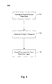
- Fig. 1 is a flowchart showing a simplified overview of a dielectric deposition according to embodiments of the invention
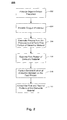
- Fig. 2 is a flowchart illustrating methods of filling a gap with a dielectric material according to embodiments of the invention
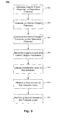
- Fig. 3 is a flowchart showing steps for depositing and annealing a dielectric material in a gap on a substrate according to embodiments of the invention
- Fig. 4 is a flowchart illustrating methods of making a multilayer silicon oxide film according to embodiments of the invention.
- Figs. 5A-F show a substrate having a gap structure that is progressively filled with a multilayer silicon oxide film according to embodiments of the invention
- Fig. 6A shows a vertical cross-sectional view of a substrate processing system that may be used to form silicon oxide layers according to embodiments of the invention.
- Fig. 6B shows a simplified diagram of a system monitor/controller component of a substrate processing system according to embodiments of the invention.
- the dielectric materials may be formed from organo-silicon compounds that have a lower ratio of carbon atoms to silicon atoms (the C:Si ratio) than conventional tetraethoxysiloxane (TEOS).
- TEOS tetraethoxysiloxane
- the dielectric films formed by combining these compounds with oxygen precursors typically have lower carbon contents, lower porosities, and lower WERRs than an initially deposited TEOS based silicon oxide. This makes the films less susceptible to cracking, void formation, water absorption, and/or shrinkage than TEOS based oxide films.
- the organo-silicon compounds may also have a oxygen atom to silicon atom ratio (the O:Si ratio) that is equal to or greater than the TEOS O:Si ratio.
- Organo-silicon precursors with low C:Si ratios and high O:Si ratios produce higher quality silicon oxide films with lower carbon content than conventionally made oxides that exclusively use TEOS as a silicon precursor.
- Embodiments also include organo-silicon precursors that have one or more Si-O-Si linkages in the molecular structure. This linkage in the Si precursor facilitates the formation of SiO x films with reduced contamination from carbon and hydroxyl groups.
- the organo-silicon compounds may also include halogenated siloxanes and silazoxanes that include halogen and nitrogen groups that can be easily oxidized into Si-O groups.
- the halogenated siloxanes may include chlorinated siloxanes such as octachlorotrisiloxane (OCTS) whose Si-C groups can be readily oxidized by molecular oxygen, ozone, nitrogen dioxide, hydrogen peroxide, etc., into Si-O groups with reduced carbon levels.
- OCTS octachlorotrisiloxane
- silazoxanes such as hexamethoxydisilazoxanes (HMDS-H) have SiN groups that can be readily oxidized into Si-O groups.
- the organo-silicon compounds may be introduced to reactive atomic oxygen precursors in the deposition chamber to further increase the formation of Si-O groups in the deposited dielectric film.
- the atomic oxygen may be initially generated outside the deposition chamber, using for example a remote high-density plasma generating unit, before being sent into the deposition chamber to react with the organo-silicon precursor.
- the resulting silicon oxide layer can have improved flowability and gap-flow characteristics, as well as lower carbon content and porosity, than conventional oxide films formed by reacting the organo-silicon precursor with molecular oxygen, ozone, etc., in the deposition chamber. Additional details about embodiments of the methods, products, and systems of the invention will now be discussed.
- Fig. 1 shows a flowchart that includes a simplified overview of a dielectric deposition according to embodiments of the invention.
- the method 100 shown includes introducing an organo-silicon precursor 102 and an oxygen precursor 104 to a deposition chamber.
- the precursors react in the chamber to form a dielectric layer in the gaps and on the surfaces of the substrate 106.
- the organo-silicon precursor introduced to the deposition chamber may have an C:Si atom ratio of less than 8 (e.g. , a C:Si ratio of 7, 6, 5, 4, 3, 2, or 1 or less). This means there are fewer than 8 carbon atoms in the organo-silicon precursor molecule for every silicon atom present.
- the tetraethoxysiloxane (TEOS) molecule shown below has 8 carbon atoms for every atom of silicon (i.e., a C:Si ratio of 8):
- the organo-silicon precursor may be a siloxane compound such as triethoxysiloxane (TRIES), tetramethoxysiloxane (TMOS), trimethoxysiloxane (TRIMOS), hexamethoxydisiloxane (HMODS), octamethoxytrisiloxane (OMOTS), and/or octamethoxydodecasiloxane (OMODDS), among other siloxane compounds:
- TRIES triethoxysiloxane
- TMOS tetramethoxysiloxane
- TRIMOS trimethoxysiloxane
- HMODS hexamethoxydisiloxane
- OOMOTS octamethoxytrisiloxane
- OMODDS octamethoxydodecasiloxane
- the organo-silicon compound may also be a silazoxane compound that includes one or more nitrogen groups.
- the silazoxane compounds may include hexamethoxydisilazoxane (HMDS-H), methyl hexamethoxydisilazoxane (HMDS-CH 3 ), chlorohexamethoxydisilazoxane (HMDS-C1), hexaethoxydislazoxane (HEDS-H), nonamethoxytrisilazoxane (NMTS), and octamethoxycyclicsilazoxane (OMCS), among other silazoxane compounds:
- the organo-silicon compound further be a halogenated siloxane compound that includes one or more halogen groups (e.g. , fluoride, chloride, bromide, or iodide groups).
- the halogenated siloxane may be a chlorinated siloxane compound such as tetrachlorosilane (TECS), dichlorodiethoxysiloxane (DCDES), chlorotriethoxysiloxane (CTES), hexachlorodisiloxane (HCDS), and/or octachlorotrisiloxane (OCTS), among other chlorinated siloxane compounds:
- TECS tetrachlorosilane
- DCDES dichlorodiethoxysiloxane
- CTES chlorotriethoxysiloxane
- HCDS hexachlorodisiloxane
- OCTS octachlorotrisiloxane
- the organo-silicon compounds may also have an O:Si ratio of about 0, 0.5, 1, 2, 3, 4, 5, 6, etc., or more.
- TMOS has an O:Si atom ratio of 4 (the same as TEOS).
- the organo-silicon precursors may further include an Si-O-Si linkage, as seen in HMODS, OMOTS, OMODDS, HCDS, and OCTS, among other organo-silicon compounds.
- This linkage in the Si precursor may facilitate the formation of SiO x films with reduced contamination from carbon and hydroxyl groups.
- the organo-silicon precursors may still further include aminosilanes such as Trisilylamine (TSA), Hexamethyldisilazane (HMDS), Silatrane, Tetrakis(dimethylamino)silane, Bis(diethylamino)silane, Tris(dimethylamino)chlorosilane, and methylsilatrane, among other compounds:
- aminosilanes such as Trisilylamine (TSA), Hexamethyldisilazane (HMDS), Silatrane, Tetrakis(dimethylamino)silane, Bis(diethylamino)silane, Tris(dimethylamino)chlorosilane, and methylsilatrane, among other compounds:
- the organo-silicon precursors may still further include disilanes including, alkoxy disilanes, alkoxy-alkyl disilanes, and alkoxy-acetoxy disilanes.
- the alkoxy disilanes may include: wherein R 1-6 may be, independently, a C 1-3 alkyloxy group.
- the alkoxy disilanes may include hexamethoxydisilane, and hexaethoxydisilane among other alkoxy disilanes.
- the alkoxy disilanes may also include cyclic disilane compounds with alkoxy groups bonded to the Si moieties.
- the alkoxycyclosilanes may include octaethoxycyclobutasilane, decabutaoxycyclopentasilane, and dodecamethoxycyclohexasilane, among others.
- the alkoxy-alkyl disilanes may include: wherein R 7-12 may be, independently, a C 1-3 alkyl group or a C 1-3 alkyloxy group, and wherein at least one of R 7-12 is a alkyl group and at least one of R 7-12 is an alkyloxy group.
- Alkoxy-alkyl disilanes may also include cyclic disilanes with alkyl and alkoxy moieties, such as butasilanes, pentasilanes, hexasilanes, heptasilane, octasilanes, etc., having at least one alkyl and alkoxy group bonded thereto.
- Examples include octamethyl-1,4-dioxa-2,3,5,6-tetrasilacyclohexane; 1,4-dioxa-2,3,5,6-tetrasilacyclohexane; and 1,2,3,4,5,6-hexamethoxy-1,2,3,4,5,6,-hexamethylcyclohexasilane, among other alkoxy-alkyl cyclosilanes.
- Alkoxy-acetoxy disilanes may include: wherein R 13-17 may be, independently, a C 1-3 alkyl group, a C 1-3 alkoxy group, or an acetoxy group, and wherein at least one of R 13-17 is a alkoxy group and at least one of R 13-17 is an acetoxy group.
- the organo-silicon precursors may yet further include organocyclosilanes such as cyclobutasilane, cyclopentasilane, cyclohexasilane, cycloheptasilane, cyclooctasilane, etc.
- organocyclosilanes such as cyclobutasilane, cyclopentasilane, cyclohexasilane, cycloheptasilane, cyclooctasilane, etc.
- the oxygen precursor may include molecular oxygen (O 2 ) , ozone (O 3 ), a nitrogen-oxygen compound (e.g. , NO, NO 2 N 2 O etc.), a hydrogen-oxygen compound ( e.g. , H 2 O H 2 O 2 etc. ) , as well as other oxygen containing precursors and combinations of precursors.
- the oxygen precursor may include atomic oxygen radicals that are remotely generated and introduced into the deposition chamber with the organo-silicon precursor.
- the method 200 may include providing a substrate to a deposition chamber, and then introducing an organo-silicon precursor 202 and an oxygen precursor 204 to the chamber.
- the substrate may be a semiconductor wafer (e.g. , a 200 mm, 300 mm, 400 mm, etc. silicon wafer) and may include structures, device components, etc., formed in earlier processes.
- the substrate may include gaps, trenches, etc., with high height to width aspect ratios (e.g., an aspect ratio of 5:1 or more, 6:1 or more, 7:1 or more, 8:1 or more, 9:1 or more, 10:1 or more, 11:1 or more, 12:1 more, etc.).
- high height to width aspect ratios e.g., an aspect ratio of 5:1 or more, 6:1 or more, 7:1 or more, 8:1 or more, 9:1 or more, 10:1 or more, 11:1 or more, 12:1 more, etc.
- the organo-silicon precursor may include a siloxane, halogenated siloxane, and/or silazoxane compound, and may include organo-silicon compounds where the C:Si atom ratio of less than 8.
- the silicon precursor may be mixed with a carrier gas before or during its introduction to the deposition chamber.
- a carrier gas may be an inactive gas that does not unduly interfere with the formation of the oxide film on the substrate. Examples of carrier gases include helium, neon, argon, and hydrogen (H 2 ), among other gases.
- the organo-silicon precursor may be introduced to the deposition chamber by mixing an organo-silicon compound (gas or liquid) with helium at a flow rate of about 600 to about 2400 sccm through the room-temperature organo-silicon precursor to provide a flow of the precursor to the chamber at a rate of about 800 to about 1600 mgm.
- an organo-silicon compound gas or liquid
- helium at a flow rate of about 600 to about 2400 sccm
- the room-temperature organo-silicon precursor to provide a flow of the precursor to the chamber at a rate of about 800 to about 1600 mgm.
- the oxygen precursor may include molecular oxygen (O 2 ) , ozone (O 3 ), a nitrogen-oxygen compound (e.g. , NO, NO 2 N 2 O etc.), a hydrogen-oxygen compound ( e.g. , H 2 O, H 2 O 2 etc. ) , a carbon-oxygen compound (e.g., CO, CO 2, etc. ) , as well as other oxygen containing precursors and combinations of precursors.
- the oxygen precursor may also include atomic oxygen radicals that are remotely generated and introduced into the deposition chamber with the organo-silicon precursor.
- the method 200 may include generating a plasma in the deposition chamber from the precursors, and forming a first portion of a dielectric material 206.
- the oxygen and organo-silicon precursors are not mixed before being introduced to the deposition chamber.
- the precursors may enter the chamber through separate spatially separated precursor inlets distributed around reaction chamber.
- the oxygen precursor may enter from an inlet (or inlets) at the top of the chamber and positioned directly above the substrate.
- the inlet directs the flow of the oxygen precursor in a direction perpendicular to the substrate deposition surface.
- the silicon precursor may enter from one or more inlets around the sides of the deposition chamber.
- the inlets may direct the flow of the silicon precursor in a direction approximately parallel to the deposition surface.
- the oxygen and organo-silicon plasma reacts in the deposition chamber, it forms the first portion of a silicon oxide dielectric layer on the substrate deposition surface.
- the initial oxide layer has excellent flowability, and can quickly migrate into gaps, trenches, voids, seams, etc., in the structures present at the deposition surface. This allows the method 200 to provide oxide fills that are substantially free of voids and seams in gaps, trenches, and other surface structures that have high height to width aspect ratios (e.g. , ARs of about 5:1, 6:1, 6:1, 8:1, 9:1, 10:1, 11:1, and 12:1 or more).
- the flow of the precursors into the chamber may stop, and the material may be etched 208.
- the etching step may be used to dissociate and remove impurities in the material, and also to planarize the material.
- the etching process may include a single-step etch, or a multistep etch.
- a multistep etch process may include first etch may include using a lower-density plasma to dissociate larger organic molecules and remove at least a portion of the carbon in the dielectric material. This lower-density plasma etch may include using an RPS system to generate an Ar/O 2 plasma that etches the oxide layer.
- the etch conditions may include, for example, striking a plasma from a flow of 1600 sccm O 2 and 400 sccm argon at a power of about 5500 Watts and introducing it to the deposition chamber at a pressure of about 760 mTorr.
- This plasma etch can dissociate larger carbon groups and remove carbon impurities from the oxide layer.
- a second etch of the oxide layer may be conducted at a higher plasma density to remove at least a portion of the hydroxyl groups in the layer.
- This higher-density plasma etch may include exposing the layer to a plasma formed from the dissociation of a flow of molecular oxygen (e.g., 600 sccm) with a high-power RF field (e.g., 6000 Watts).
- the oxygen plasma may be introduced to the deposition chamber at a pressure of, for example, 8 mTorr, and react with the -OH groups in the oxide layer to form silicon dioxide and water.
- the precursors are reintroduced to the deposition chamber, and react to form a second portion of dielectric material in the gap and other surfaces of the substrate 210.
- the second portion may also be an oxide layer formed under the same reaction conditions as the first layer, or may be formed under a different conditions ( e.g. , chamber pressure, temperature, organo-silicon precursor, etc. ) .
- the second layer After the second layer has been formed it also may be etched to reduce impurity levels and/or planarize the layer.
- the second layer may be etched using the same process as used to etch the first layer, or may be etched using a different process, ( e.g. , different number of etching steps, different etch precursors, different power level, etc.).
- the material may be annealed 212 to form a uniform, high-quality silicon oxide gapfill.
- the final gapfill may have a dielectric constant (i.e., k-value) of less than 3.0, and a wet-etch rate ratio (WERR) of less than 2:1 ( e.g. , about 1.8:1 to about 1.4:1).
- WERR wet-etch rate ratio
- the gapfill may be uniform throughout the fill volume, and contain few, if any, voids or seams.
- Fig. 3 is a flowchart showing steps for depositing and annealing a dielectric material in a gap on a substrate according to additional embodiments of the invention.
- the method 300 includes introducing the organo-silicon precursor to the deposition chamber 302.
- the method 300 also includes generating a highly reactive atomic oxygen precursor 304 by the dissociation of an oxygen containing precursor such as molecular oxygen (O 2 ), ozone (O 3 ), an nitrogen-oxygen compound (e.g.
- a hydrogen-oxygen compound e.g., H 2 O H 2 O 2 , etc.
- a carbon-oxygen compound e.g., CO, CO 2 , etc.
- the oxygen containing precursor may be dissociated remotely to make the atomic oxygen.
- the dissociation process may include thermal dissociation, ultraviolet light dissociation, and/or plasma dissociation, among other methods.
- Plasma dissociation may involve striking a plasma from helium, argon, etc., in a remote plasma generating chamber and introducing the oxygen precursor to the plasma to generate the atomic oxygen precursor.
- the atomic oxygen may be generated in a remote high-density plasma generator supplying 4000 to 6000 Watts ( e.g.
- the reactive atomic oxygen plasma is then introduced to the deposition chamber 306, where it may mix for the first time with the organo-silicon precursor, which is also introduced to the chamber.
- the highly reactive atomic oxygen will react with the silicon precursor 308 (and other deposition precursors that may be present in the reaction chamber) at moderate temperatures (e.g. , reaction temperatures less than 100°C) and pressures (e.g., 0.5 to 6 Torr total chamber pressure).
- Embodiments include sending the atomic oxygen and silicon precursors through separate ports of a multi-port showerhead.
- a showerhead positioned above the substrate may include a pattern of openings for the precursors to enter the deposition chamber.
- One subset of openings may be supplied by the atomic oxygen precursor, while a second subset of openings is supplied by the silicon precursor.
- Precursors traveling through different sets of opening may be fluidly isolated from each other until exiting into the deposition chamber. Additional details about types and designs of precursor handling equipment is described in co-assigned U.S. Provisional Patent App. No. 60/803,499 to Lubomirsky et al, filed May 30, 2006 , and titled "PROCESS CHAMBER FOR DIELECTRIC GAPFILL,” the entire contents of which are hereby incorporated by reference for all purposes.
- the dielectric layer is deposited on the substrate 310.
- the total pressure in the chamber during the deposition may be, for example, about 0.5 Torr to about 6 Torr. Higher total pressures (e.g. , 1.3 Torr) may deposit a oxide film with more flow-like qualities, while lower pressures ( e.g. , 0.5 Torr) may deposit a more conformal oxide layer.
- the deposition temperature in the reaction chamber may be relatively low ( e.g. , about 100°C or less).
- the deposition rates may range from about 500 ⁇ /min to about 3000 ⁇ /min ( e.g. , 1500 ⁇ /min).
- the thickness of the layer may be about 50 ⁇ to about 500 ⁇ ( e.g. , about 100 ⁇ to about 200 ⁇ ).
- a first anneal may be performed 312 that removes a portion of the moisture and increases the hardness of the layer.
- This initial anneal step may include heating the oxide layer for about 1 minute to 10 minutes in an inert environment (e.g., a dry-N 2 environment).
- a thermal anneal temperature may be selected that will not damage metal lines formed in the substrate structure, such as when the oxide layer is an intermetal dielectric being deposited over an aluminum metal lines.
- the first anneal step may include exposing the silicon oxide layer to ultra-violet (UV) light for about 1 minute to about 30 minutes.
- UV ultra-violet
- a UV anneal may remove a portion of the moisture present in the initially deposited oxide film, and also increase the hardness of the film.
- a second anneal step may be performed 314 to further remove moisture and silanol bonds from the oxide layer.
- this anneal step 314 substantially all of the moisture and silanol may be removed to give the layer a lower k-value and lower WERR value than either the initially deposited oxide or after the layer was treated in the first anneal step.
- This second anneal may include exposing the oxide layer to a plasma that is efficient at removing water and silanol groups from the dielectric oxide. Following the first anneal, however, the oxide layer has sufficient hardness to reduce (or prevent) the plasma from disrupting the carbon groups present in the oxide. Thus, for low-k, carbon containing oxide layers, the plasma anneal does not remove enough carbon to increase significantly the k-value of the layer.
- the method 400 includes providing a substrate to a deposition chamber 402 and introducing precursors (e.g. , atomic oxygen and organo-silicon precursors) to the chamber 404.
- precursors e.g. , atomic oxygen and organo-silicon precursors
- the precursors react to form a silicon oxide layer on the substrate 406, and then the oxide layer may be etched 408.
- a check may be made to determine if the cumulative thickness of the deposited oxide layers has reached a preset point 410. If the preset thickness level of the total oxide film has been reached, then the deposition and etch cycle may end, and the film may be annealed 412. However, if the thickness level has not been met, then another oxide deposition and etch cycle may occur to add at least one more additional layer to the oxide film.
- Determining whether the oxide film has reached a predetermined thickness may be done by a thickness measurement of the deposited and etched layers, or may be done by calculating the number of layers need to reach a desired film thickness. For example, if each deposited and etched layer is 100 ⁇ thick, and the desired film thickness 1.2 ⁇ m, then 12 deposition and etch cycles should be done to form the film.
- the thickness of each deposited layer may be set by controlling the parameters that effect the oxide deposition rate, such as the types and flow rates of the reactive precursors, the total pressure in the deposition chamber, and the temperature, among other parameters. As noted above, typical deposition rates for the oxide layers are about 500 ⁇ /min to about 3000 ⁇ /min ( e.g. , about 1500 ⁇ /min).
- Figs. 5A-F show a substrate having a gap structure that is progressively filled with a multilayer silicon oxide film using embodiments of the multicycle deposition-etch oxide layer formation process.
- Fig. 5A shows a substrate 502 on which a gap 504 has been formed. It will be appreciated that gap 504 shown in Figs. 5A-F has been drawn with a relatively low aspect ratio to more clearly show the progression of the oxide fill layers.
- Embodiments of the present gapfill methods may include void and seam free depositions into gaps having aspect ratios of 5:1, 6:1, 7:1, 8:1, 9:1, 10:1, 11:1, 12:1, 13:1, 14:1, and 15:1 or more.
- Fig. 5B shows a first oxide layer 506a deposited in gap 504.
- the silicon oxide that formed the layer has good flowability qualities, allowing the film to quickly migrate to the bottom of gap 504.
- the thickness of the deposited oxide at the bottom of the gap 504 may be greater than the oxide thickness along the sidewalls of the gap.
- Figs. 5C and D show additional oxide layers 506b, 506c, etc., being deposited on previously deposited and etched layers in the gap 504. These additional layers may be formed from the bottom up in the gap 504, until a desired oxide film thickness level is reached ( e.g. , the top of gap 504).
- anneal may be conducted to form the layers into a uniform film 508, as shown in Fig. 5E .
- the film may be planarized by, for example, plasma etching or CMP to remove deposition materials formed over the top of the gap 504.
- Fig. 5F shows the remaining silicon oxide gapfill 510, having few, if any, voids or seams, and having high film-quality and dielectric characteristics.
- Deposition systems may include high-density plasma chemical vapor deposition (HDP-CVD) systems, plasma enhanced chemical vapor deposition (PECVD) systems, sub-atmospheric chemical vapor deposition (SACVD) systems, and thermal chemical vapor deposition systems, among other types of systems.
- HDP-CVD high-density plasma chemical vapor deposition
- PECVD plasma enhanced chemical vapor deposition
- SACVD sub-atmospheric chemical vapor deposition
- thermal chemical vapor deposition systems among other types of systems.
- Specific examples of CVD systems include the CENTURA ULTIMATM HDP-CVD chambers/systems, and PRODUCERTM PECVD chambers/systems, available from Applied Materials, Inc. of Santa Clara, California.
- Examples of substrate processing systems that can be used with exemplary methods of the invention may include those shown and described in co-assigned U.S. Provisional Patent App. No. 60/803,499 to Lubomirsky et al, filed May 30, 2006 , and titled "PROCESS CHAMBER FOR DIELECTRIC GAPFILL," the entire contents of which is herein incorporated by reference for all purposes. Additional exemplary systems may include those shown and described in U.S. Pat. Nos. 6,387,207 and 6,830,624 , which are also incorporated herein by reference for all purposes.
- FIG. 6A vertical cross-sectional views of a CVD system 10 is shown that has a vacuum or processing chamber 15 that includes a chamber wall 15a and a chamber lid assembly 15b.
- the CVD system 10 contains a gas distribution manifold 11 for dispersing process gases to a substrate (not shown) that rests on a heated pedestal 12 centered within the process chamber 15.
- Gas distribution manifold 11 may be formed from an electrically conducting material in order to serve as an electrode for forming a capacitive plasma.
- the substrate e.g. a semiconductor wafer
- the substrate e.g. a semiconductor wafer
- the substrate is positioned on a flat (or slightly convex) surface 12a of the pedestal 12.
- the pedestal 12 can be moved controllably between a lower loading/off-loading position (depicted in FIG. 6A ) and an upper processing position (indicated by dashed line 14 in FIG. 6A ), which is closely adjacent to the manifold 11.
- a centerboard (not shown) includes sensors for providing information on the position of the wafers.
- Deposition and carrier gases are introduced into the chamber 15 through perforated holes 13b of a conventional flat, circular gas distribution faceplate 13a. More specifically, deposition process gases flow into the chamber through the inlet manifold 11, through a conventional perforated blocker plate 42 and then through holes 13b in gas distribution faceplate 13a.
- the supply line for each process gas includes (i) several safety shut-off valves (not shown) that can be used to automatically or manually shut-off the flow of process gas into the chamber, and (ii) mass flow controllers (also not shown) that measure the flow of gas through the supply line.
- the several safety shut-off valves are positioned on each gas supply line in conventional configurations.
- the deposition process performed in the CVD system 10 can be either a thermal process or a plasma-enhanced process.
- an RF power supply 44 applies electrical power between the gas distribution faceplate 13a and the pedestal 12 so as to excite the process gas mixture to form a plasma within the cylindrical region between the faceplate 13a and the pedestal 12. (This region will be referred to herein as the "reaction region"). Constituents of the plasma react to deposit a desired film on the surface of the semiconductor wafer supported on pedestal 12.
- RF power supply 44 is a mixed frequency RF power supply that typically supplies power at a high RF frequency (RF1) of 13.56 MHz and at a low RF frequency (RF2) of 360 KHz to enhance the decomposition of reactive species introduced into the vacuum chamber 15.
- RF1 high RF frequency
- RF2 low RF frequency
- the RF power supply 44 would not be utilized, and the process gas mixture thermally reacts to deposit the desired films on the surface of the semiconductor wafer supported on the pedestal 12, which is resistively heated to provide thermal energy for the reaction.
- the plasma heats the entire process chamber 10, including the walls of the chamber body 15a surrounding the exhaust passageway 23 and the shut-off valve 24.
- a hot liquid is circulated through the walls 15a of the process chamber 15 to maintain the chamber at an elevated temperature.
- the passages in the remainder of the chamber walls 15a are not shown.
- Fluids used to heat the chamber walls 15a include the typical fluid types, i.e., water-based ethylene glycol or oil-based thermal transfer fluids.
- heating beneficially reduces or eliminates condensation of undesirable reactant products and improves the elimination of volatile products of the process gases and other contaminants that might contaminate the process if they were to condense on the walls of cool vacuum passages and migrate back into the processing chamber during periods of no gas flow.
- the remainder of the gas mixture that is not deposited in a layer, including reaction byproducts, is evacuated from the chamber 15 by a vacuum pump (not shown). Specifically, the gases are exhausted through an annular, slot-shaped orifice 16 surrounding the reaction region and into an annular exhaust plenum 17.
- the annular slot 16 and the plenum 17 are defined by the gap between the top of the chamber's cylindrical side wall 15a (including the upper dielectric lining 19 on the wall) and the bottom of the circular chamber lid 20.
- the 360.degree. circular symmetry and uniformity of the slot orifice 16 and the plenum 17 are important to achieving a uniform flow of process gases over the wafer so as to deposit a uniform film on the wafer.
- the gases flow underneath a lateral extension portion 21 of the exhaust plenum 17, past a viewing port (not shown), through a downward-extending gas passage 23, past a vacuum shut-off valve 24 (whose body is integrated with the lower chamber wall 15a), and into the exhaust outlet 25 that connects to the external vacuum pump (not shown) through a foreline (also not shown).
- the wafer support platter of the pedestal 12 (preferably aluminum, ceramic, or a combination thereof) is resistively heated using an embedded single-loop embedded heater element configured to make two full turns in the form of parallel concentric circles.
- An outer portion of the heater element runs adjacent to a perimeter of the support platter, while an inner portion runs on the path of a concentric circle having a smaller radius.
- the wiring to the heater element passes through the stem of the pedestal 12.
- any or all of the chamber lining, gas inlet manifold faceplate, and various other reactor hardware are made out of material such as aluminum, anodized aluminum, or ceramic.
- An example of such a CVD apparatus is described in co-assigned U.S. Pat. No. 5,558,717 entitled “CVD Processing Chamber,” issued to Zhao et al, and hereby incorporated by reference in its entirety.
- a lift mechanism and motor 32 raises and lowers the heater pedestal assembly 12 and its wafer lift pins 12b as wafers are transferred into and out of the body of the chamber 15 by a robot blade (not shown) through an insertion/removal opening 26 in the side of the chamber 10.
- the motor 32 raises and lowers pedestal 12 between a processing position 14 and a lower, wafer-loading position.
- the motor, valves or flow controllers connected to the supply lines 8, gas delivery system, throttle valve, RF power supply 44, and chamber and substrate heating systems are all controlled by a system controller over control lines 36, of which only some are shown.
- Controller 34 relies on feedback from optical sensors to determine the position of movable mechanical assemblies such as the throttle valve and susceptor which are moved by appropriate motors under the control of controller 34.
- the system controller includes a hard disk drive (memory 38), a floppy disk drive and a processor 37.
- the processor contains a single-board computer (SBC), analog and digital input/output boards, interface boards and stepper motor controller boards.
- SBC single-board computer
- Various parts of CVD system 10 conform to the Versa Modular European (VME) standard which defines board, card cage, and connector dimensions and types.
- VME Versa Modular European
- the VME standard also defines the bus structure as having a 16-bit data bus and a 24-bit address bus.
- System controller 34 controls all of the activities of the CVD machine.
- the system controller executes system control software, which is a computer program stored in a computer-readable medium such as a memory 38.
- a computer-readable medium such as a memory 38.
- the memory 38 is a hard disk drive, but the memory 38 may also be other kinds of memory.
- the computer program includes sets of instructions that dictate the timing, mixture of gases, chamber pressure, chamber temperature, RF power levels, susceptor position, and other parameters of a particular process.
- Other computer programs stored on other memory devices including, for example, a floppy disk or other another appropriate drive, may also be used to operate controller 34.
- a process for depositing a film on a substrate or a process for cleaning the chamber 15 can be implemented using a computer program product that is executed by the controller 34.
- the computer program code can be written in any conventional computer readable programming language: for example, 68000 assembly language, C, C++, Pascal, Fortran or others. Suitable program code is entered into a single file, or multiple files, using a conventional text editor, and stored or embodied in a computer usable medium, such as a memory system of the computer. If the entered code text is in a high level language, the code is compiled, and the resultant compiler code is then linked with an object code of precompiled Microsoft Windows® library routines. To execute the linked, compiled object code the system user invokes the object code, causing the computer system to load the code in memory. The CPU then reads and executes the code to perform the tasks identified in the program.
- FIG. 6B is a simplified diagram of the system monitor and CVD system 10 in a substrate processing system, which may include one or more chambers.
- two monitors 50a are used, one mounted in the clean room wall for the operators and the other behind the wall for the service technicians.
- the monitors 50a simultaneously display the same information, but only one light pen 50b is enabled.
- a light sensor in the tip of light pen 50b detects light emitted by CRT display. To select a particular screen or function, the operator touches a designated area of the display screen and pushes the button on the pen 50b.
- the touched area changes its highlighted color, or a new menu or screen is displayed, confirming communication between the light pen and the display screen.
- Other devices such as a keyboard, mouse, or other pointing or communication device, may be used instead of or in addition to light pen 50b to allow the user to communicate with controller 34.
- FIG. 6A shows a remote plasma generator 60 mounted on the lid assembly 15b of the process chamber 15 including the gas distribution faceplate 13a and the gas distribution manifold 11.
- a mounting adaptor 64 mounts the remote plasma generator 60 on the lid assembly 15b, as best seen in FIG. 6A .
- the adaptor 64 is typically made of metal.
- a mixing device 70 is coupled to the upstream side of the gas distribution manifold 11 ( FIG. 6A ).
- the mixing device 70 includes a mixing insert 72 disposed inside a slot 74 of a mixing block for mixing process gases.
- a ceramic isolator 66 is placed between the mounting adaptor 64 and the mixing device 70 ( FIGS. 6A ).
- the ceramic isolator 66 may be made of a ceramic material such as Al 2 O 3 (99% purity), Teflon®, or the like. When installed, the mixing device 70 and ceramic isolator 66 may form part of the lid assembly 15b. The isolator 66 isolates the metal adaptor 64 from the mixing device 70 and gas distribution manifold 11 to minimize the potential for a secondary plasma to form in the lid assembly 15b as discussed in more detail below.
- a three-way valve 77 controls the flow of the process gases to the process chamber 15 either directly or through the remote plasma generator 60.
- the remote plasma generator 60 is desirably a compact, self-contained unit that can be conveniently mounted on the lid assembly 15b and be easily retrofitted onto existing chambers without costly and time-consuming modifications.
- One suitable unit is the ASTRON® generator available from Applied Science and Technology, Inc. of Woburn, Mass.
- the ASTRON® generator utilizes a low-field toroidal plasma to dissociate a process gas.
- the plasma dissociates a process gas including a fluorine-containing gas such as NF 3 and a carrier gas such as argon to generate free fluorine which is used to clean film deposits in the process chamber 15.
- a method of depositing a dielectric layer in a gap formed on a substrate includes introducing an organo-silicon precursor and an oxygen precursor to a deposition chamber, wherein the organo-silicon precursor has a C:Si atom ratio of less than 8, and wherein the oxygen precursor comprises atomic oxygen that is generated outside the deposition chamber, and reacting the precursors to form the dielectric layer in the gap.
- the organo-silicon precursor can have an O:Si ratio of greater than 3; the organo-silicon precursor can have an O:Si ratio of greater than 4; the organo-silicon precursor can include a Si-O-Si bond; the organo-silicon precursor Can include a siloxane, for example, wherein the siloxane is selected from the group consisting of triethoxysiloxane, tetramethoxysiloxane, trimethoxysiloxane, hexamethoxydisiloxane, octamethoxytrisiloxane, and octamethoxydodecasiloxane; the organo-silicon precursor can include a silazoxane, for example, wherein the silazoxane is selected from the group consisting of hexamethoxydisilazoxane, methyl hex
- the atomic oxygen can be formed by forming a plasma form a gas mixture comprising argon and introducing an oxygen source to the plasma, wherein the oxygen source dissociates to form the atomic oxygen;
- the oxygen source can include molecular oxygen, ozone or nitrogen dioxide;
- the method can further include forming a plasma in the deposition chamber from the organo-silicion and oxygen precursors;
- the method can further include etching the dielectric layer to reduce the carbon content in the layer; and/or the method can further include annealing the dielectric layer in the gap.
- a method of depositing and annealing a dielectric material in a gap on a substrate is provided.
- the method includes providing an organo-silicon precursor and an oxygen precursor to a deposition chamber, wherein the organo-silicon precursor has a C:Si atom ratio of less than 8, reacting the precursors to deposit the dielectric material in the gap, performing a thermal anneal on the deposited dielectric material, and performing a plasma anneal on the deposited dielectric material.
- the thermal anneal can include heating the dielectric material to a temperature of about 300°C to about 600°C for about 1 minute to about 30 minutes;
- the plasma anneal can include exposing the dielectric material to a high-density plasma for about 1 minute to about 10 minutes;
- the organo-silicon precursor can have a C:Si ratio of about 6 or less;
- the organo-silicon precursor can have an O:Si ratio of about 3 or more;
- the organo-silicon precursor can have a Si-O-Si bond;
- the organo-silicon precursor can include a siloxane;
- the organo-silicon precursor can include a silazoxane or a halogenated siloxane;
- the oxygen precursor can include atomic oxygen that is generated outside the deposition chamber.
Abstract
Description
- This application is related to co-assigned
U.S. Provisional Patent App. Ser. No. 60/803,493 to Ingle et al, filed May 30, 2006 U.S. Prov. Pat. App. Ser. No. 60/803,481 to Chen et al, filed May 30, 2006 U.S. Prov. Pat. App. Ser. No. 60/803,489 to Munro et al, filed May 30, 2006 U.S. Prov. Pat. App. Ser. No. 60/805,573 to Lubomirsky, filed June 22, 2006 - Semiconductor device geometries have dramatically decreased in size since their introduction several decades ago. Modern semiconductor fabrication equipment routinely produces devices with 250nm, 180nm, and 65nm feature sizes, and new equipment is being developed and implemented to make devices with even smaller geometries. The smaller sizes, however, mean device elements have to work closer together which can increase the chances of electrical interference, including cross-talk and parasitic capacitance.
- To reduce the degree of electrical interference, dielectric insulating materials are used to fill the gaps, trenches, and other spaces between the device elements, metal lines, and other device features. The dielectric materials are chosen for their ease of formation in the spaces between device features, and their low dielectric constants (i.e., "k-values"). Dielectrics with lower k-values are better at minimizing cross-talk and RC time delays, as well as reducing the overall power consumption of the device. Conventional dielectric materials include silicon oxide, which has an average k-value between 4.0 and 4.2 when deposited with conventional CVD techniques.
- While the k-value of conventional CVD silicon oxide is acceptable for many device structures, the ever decreasing sizes and increasing densities of device elements have kept semiconductor manufacturers looking for dielectric materials with lower k-values. One approach has been to dope the silicon oxide with fluorine to make a fluorine-doped silicon oxide film (i.e., "FSG" film) with a dielectric constant as low as about 3.4 to 3.6. Another has been the development of spin-on glass techniques that coat the substrate with highly flowable precursors like hydrogen silsesquioxane (HSQ) to form a porous low-k film.
- More recently, silicon-oxygen-carbon (Si-O-C) films have been developed with k-values of 3.0 or less. These low-k films are often deposited by the chemical vapor deposition of carbon-silicon and oxygen precursors on the substrate. While these Si-O-C films have lower k-values than pure and fluorine-doped silicon oxide films, they also tend to be substantially more porous, which can have negative consequences. Porous films are prone to increased absorption of water, which can increase the k-value of the film. Porous films also have higher "wet etch rate ratios" (WERRs) that can make the film more prone to corrosion and stress cracking. Thus, there is a need for new methods of depositing low-k carbon based films with reduced porosity, lower WERR values, and less cracking. These and other issues are addressed by embodiments of the invention.
- Embodiments of the invention include methods of depositing a dielectric layer in a gap formed on a substrate. The methods may include the step of introducing an organo-silicon precursor and an oxygen precursor to a deposition chamber. The organo-silicon precursor may have a C:Si atom ratio of less than 8, and the oxygen precursor may include atomic oxygen generated outside the deposition chamber. The methods may also include reacting the precursors to form the dielectric layer in the gap.
- Embodiments of the invention also include methods of filling a gap with a dielectric material. The methods may include the step of providing an organo-silicon precursor and an oxygen precursor to a deposition chamber, where the organo-silicon precursor has a C:Si atom ratio of less than 8. A plasma may be generated from the precursors in the deposition chamber, where the plasma deposits a first portion of the dielectric material in the gap. The methods may also include etching the first portion of the dielectric material to reduce the carbon content in the material, and depositing a second portion of the dielectric material in the gap. The first and second portions of the dielectric material in the gap may be annealed.
- Embodiments of the invention still further include methods of depositing and annealing a dielectric material in a gap on a substrate. The methods may include the step of providing an organo-silicon precursor and an oxygen precursor to a deposition chamber, where the organo-silicon precursor has a C:Si atom ratio of less than 8. The precursors are reacted to deposit the dielectric material in the gap, and a thermal anneal may be performed on the deposited dielectric material. In addition, a plasma anneal may also be performed on the deposited dielectric material.
- Additional embodiments and features are set forth in part in the description that follows, and in part will become apparent to those skilled in the art upon examination of the specification or may be learned by the practice of the invention. The features and advantages of the invention may be realized and attained by means of the instrumentalities, combinations, and methods described in the specification.
- A further understanding of the nature and advantages of the present invention may be realized by reference to the remaining portions of the specification and the drawings wherein like reference numerals are used throughout the several drawings to refer to similar components. In some instances, a sublabel is associated with a reference numeral and follows a hyphen to denote one of multiple similar components. When reference is made to a reference numeral without specification to an existing sublabel, it is intended to refer to all such multiple similar components.
-
Fig. 1 is a flowchart showing a simplified overview of a dielectric deposition according to embodiments of the invention; -
Fig. 2 is a flowchart illustrating methods of filling a gap with a dielectric material according to embodiments of the invention; -
Fig. 3 is a flowchart showing steps for depositing and annealing a dielectric material in a gap on a substrate according to embodiments of the invention; -
Fig. 4 is a flowchart illustrating methods of making a multilayer silicon oxide film according to embodiments of the invention; -
Figs. 5A-F show a substrate having a gap structure that is progressively filled with a multilayer silicon oxide film according to embodiments of the invention; -
Fig. 6A shows a vertical cross-sectional view of a substrate processing system that may be used to form silicon oxide layers according to embodiments of the invention; and -
Fig. 6B shows a simplified diagram of a system monitor/controller component of a substrate processing system according to embodiments of the invention. - Systems and methods are described for depositing dielectric materials in gaps and on surfaces on a substrate. The dielectric materials may be formed from organo-silicon compounds that have a lower ratio of carbon atoms to silicon atoms (the C:Si ratio) than conventional tetraethoxysiloxane (TEOS). The dielectric films formed by combining these compounds with oxygen precursors typically have lower carbon contents, lower porosities, and lower WERRs than an initially deposited TEOS based silicon oxide. This makes the films less susceptible to cracking, void formation, water absorption, and/or shrinkage than TEOS based oxide films.
- The organo-silicon compounds may also have a oxygen atom to silicon atom ratio (the O:Si ratio) that is equal to or greater than the TEOS O:Si ratio. Organo-silicon precursors with low C:Si ratios and high O:Si ratios produce higher quality silicon oxide films with lower carbon content than conventionally made oxides that exclusively use TEOS as a silicon precursor. Embodiments also include organo-silicon precursors that have one or more Si-O-Si linkages in the molecular structure. This linkage in the Si precursor facilitates the formation of SiOx films with reduced contamination from carbon and hydroxyl groups.
- The organo-silicon compounds may also include halogenated siloxanes and silazoxanes that include halogen and nitrogen groups that can be easily oxidized into Si-O groups. The halogenated siloxanes may include chlorinated siloxanes such as octachlorotrisiloxane (OCTS) whose Si-C groups can be readily oxidized by molecular oxygen, ozone, nitrogen dioxide, hydrogen peroxide, etc., into Si-O groups with reduced carbon levels. Similarly, silazoxanes such as hexamethoxydisilazoxanes (HMDS-H) have SiN groups that can be readily oxidized into Si-O groups.
- The organo-silicon compounds may be introduced to reactive atomic oxygen precursors in the deposition chamber to further increase the formation of Si-O groups in the deposited dielectric film. The atomic oxygen may be initially generated outside the deposition chamber, using for example a remote high-density plasma generating unit, before being sent into the deposition chamber to react with the organo-silicon precursor. The resulting silicon oxide layer can have improved flowability and gap-flow characteristics, as well as lower carbon content and porosity, than conventional oxide films formed by reacting the organo-silicon precursor with molecular oxygen, ozone, etc., in the deposition chamber. Additional details about embodiments of the methods, products, and systems of the invention will now be discussed.
-
Fig. 1 shows a flowchart that includes a simplified overview of a dielectric deposition according to embodiments of the invention. Themethod 100 shown includes introducing an organo-silicon precursor 102 and anoxygen precursor 104 to a deposition chamber. The precursors react in the chamber to form a dielectric layer in the gaps and on the surfaces of thesubstrate 106. - The organo-silicon precursor introduced to the deposition chamber may have an C:Si atom ratio of less than 8 (e.g., a C:Si ratio of 7, 6, 5, 4, 3, 2, or 1 or less). This means there are fewer than 8 carbon atoms in the organo-silicon precursor molecule for every silicon atom present. By comparison, the tetraethoxysiloxane (TEOS) molecule shown below has 8 carbon atoms for every atom of silicon (i.e., a C:Si ratio of 8):

- The organo-silicon precursor may be a siloxane compound such as triethoxysiloxane (TRIES), tetramethoxysiloxane (TMOS), trimethoxysiloxane (TRIMOS), hexamethoxydisiloxane (HMODS), octamethoxytrisiloxane (OMOTS), and/or octamethoxydodecasiloxane (OMODDS), among other siloxane compounds:


- The organo-silicon compound may also be a silazoxane compound that includes one or more nitrogen groups. The silazoxane compounds may include hexamethoxydisilazoxane (HMDS-H), methyl hexamethoxydisilazoxane (HMDS-CH3), chlorohexamethoxydisilazoxane (HMDS-C1), hexaethoxydislazoxane (HEDS-H), nonamethoxytrisilazoxane (NMTS), and octamethoxycyclicsilazoxane (OMCS), among other silazoxane compounds:


- The organo-silicon compound further be a halogenated siloxane compound that includes one or more halogen groups (e.g., fluoride, chloride, bromide, or iodide groups). For example, the halogenated siloxane may be a chlorinated siloxane compound such as tetrachlorosilane (TECS), dichlorodiethoxysiloxane (DCDES), chlorotriethoxysiloxane (CTES), hexachlorodisiloxane (HCDS), and/or octachlorotrisiloxane (OCTS), among other chlorinated siloxane compounds:


- The organo-silicon compounds may also have an O:Si ratio of about 0, 0.5, 1, 2, 3, 4, 5, 6, etc., or more. For example, TMOS has an O:Si atom ratio of 4 (the same as TEOS). Other organo-silicon compounds, such as TRIES, and TRIMOS, have an O:Si ratio of 3. Still others, such as HCDS have an O:Si ratio of 0.5, and TECS has an O:Si ratio of 0.
- The organo-silicon precursors may further include an Si-O-Si linkage, as seen in HMODS, OMOTS, OMODDS, HCDS, and OCTS, among other organo-silicon compounds. This linkage in the Si precursor may facilitate the formation of SiOx films with reduced contamination from carbon and hydroxyl groups.
- The organo-silicon precursors may still further include aminosilanes such as Trisilylamine (TSA), Hexamethyldisilazane (HMDS), Silatrane, Tetrakis(dimethylamino)silane, Bis(diethylamino)silane, Tris(dimethylamino)chlorosilane, and methylsilatrane, among other compounds:


- The organo-silicon precursors may still further include disilanes including, alkoxy disilanes, alkoxy-alkyl disilanes, and alkoxy-acetoxy disilanes. The alkoxy disilanes may include:

- The alkoxy disilanes may also include cyclic disilane compounds with alkoxy groups bonded to the Si moieties. For example the alkoxycyclosilanes may include octaethoxycyclobutasilane, decabutaoxycyclopentasilane, and dodecamethoxycyclohexasilane, among others. Some examples of alkoxy disilanes are shown below:


- The alkoxy-alkyl disilanes may include:


- Alkoxy-acetoxy disilanes may include:

- The organo-silicon precursors may yet further include organocyclosilanes such as cyclobutasilane, cyclopentasilane, cyclohexasilane, cycloheptasilane, cyclooctasilane, etc.
- The oxygen precursor may include molecular oxygen (O2), ozone (O3), a nitrogen-oxygen compound (e.g., NO, NO2 N2O etc.), a hydrogen-oxygen compound (e.g., H2O H2O2 etc.), as well as other oxygen containing precursors and combinations of precursors. In some embodiments, the oxygen precursor may include atomic oxygen radicals that are remotely generated and introduced into the deposition chamber with the organo-silicon precursor.
- Referring now to
Fig. 2 , a flowchart illustrating amethod 200 of filling a gap with a dielectric material according to embodiments of the invention is shown. Themethod 200 may include providing a substrate to a deposition chamber, and then introducing an organo-silicon precursor 202 and anoxygen precursor 204 to the chamber. The substrate may be a semiconductor wafer (e.g., a 200 mm, 300 mm, 400 mm, etc. silicon wafer) and may include structures, device components, etc., formed in earlier processes. For example, the substrate may include gaps, trenches, etc., with high height to width aspect ratios (e.g., an aspect ratio of 5:1 or more, 6:1 or more, 7:1 or more, 8:1 or more, 9:1 or more, 10:1 or more, 11:1 or more, 12:1 more, etc.). The where the dielectric material is deposited in the gap and other surfaces of the substrate. - As noted above, the organo-silicon precursor may include a siloxane, halogenated siloxane, and/or silazoxane compound, and may include organo-silicon compounds where the C:Si atom ratio of less than 8. The silicon precursor may be mixed with a carrier gas before or during its introduction to the deposition chamber. A carrier gas may be an inactive gas that does not unduly interfere with the formation of the oxide film on the substrate. Examples of carrier gases include helium, neon, argon, and hydrogen (H2), among other gases.
- For example, the organo-silicon precursor may be introduced to the deposition chamber by mixing an organo-silicon compound (gas or liquid) with helium at a flow rate of about 600 to about 2400 sccm through the room-temperature organo-silicon precursor to provide a flow of the precursor to the chamber at a rate of about 800 to about 1600 mgm.
- The oxygen precursor may include molecular oxygen (O2), ozone (O3), a nitrogen-oxygen compound (e.g., NO, NO2 N2O etc.), a hydrogen-oxygen compound (e.g., H2O, H2O2 etc.), a carbon-oxygen compound (e.g., CO, CO2, etc.), as well as other oxygen containing precursors and combinations of precursors. As described in more detail below for
method 300, the oxygen precursor may also include atomic oxygen radicals that are remotely generated and introduced into the deposition chamber with the organo-silicon precursor. - The
method 200 may include generating a plasma in the deposition chamber from the precursors, and forming a first portion of adielectric material 206. In embodiments ofmethod 200, the oxygen and organo-silicon precursors are not mixed before being introduced to the deposition chamber. The precursors may enter the chamber through separate spatially separated precursor inlets distributed around reaction chamber. For example, the oxygen precursor may enter from an inlet (or inlets) at the top of the chamber and positioned directly above the substrate. The inlet directs the flow of the oxygen precursor in a direction perpendicular to the substrate deposition surface. Meanwhile, the silicon precursor may enter from one or more inlets around the sides of the deposition chamber. The inlets may direct the flow of the silicon precursor in a direction approximately parallel to the deposition surface. - As the oxygen and organo-silicon plasma reacts in the deposition chamber, it forms the first portion of a silicon oxide dielectric layer on the substrate deposition surface. The initial oxide layer has excellent flowability, and can quickly migrate into gaps, trenches, voids, seams, etc., in the structures present at the deposition surface. This allows the
method 200 to provide oxide fills that are substantially free of voids and seams in gaps, trenches, and other surface structures that have high height to width aspect ratios (e.g., ARs of about 5:1, 6:1, 6:1, 8:1, 9:1, 10:1, 11:1, and 12:1 or more). - After the first portion of the dielectric material is formed, the flow of the precursors into the chamber may stop, and the material may be etched 208. The etching step may be used to dissociate and remove impurities in the material, and also to planarize the material. The etching process may include a single-step etch, or a multistep etch. A multistep etch process may include first etch may include using a lower-density plasma to dissociate larger organic molecules and remove at least a portion of the carbon in the dielectric material. This lower-density plasma etch may include using an RPS system to generate an Ar/O2 plasma that etches the oxide layer. The etch conditions may include, for example, striking a plasma from a flow of 1600 sccm O2 and 400 sccm argon at a power of about 5500 Watts and introducing it to the deposition chamber at a pressure of about 760 mTorr. This plasma etch can dissociate larger carbon groups and remove carbon impurities from the oxide layer.
- Following this etch, a second etch of the oxide layer may be conducted at a higher plasma density to remove at least a portion of the hydroxyl groups in the layer. This higher-density plasma etch may include exposing the layer to a plasma formed from the dissociation of a flow of molecular oxygen (e.g., 600 sccm) with a high-power RF field (e.g., 6000 Watts). The oxygen plasma may be introduced to the deposition chamber at a pressure of, for example, 8 mTorr, and react with the -OH groups in the oxide layer to form silicon dioxide and water.
- Following the etching of the first layer, the precursors are reintroduced to the deposition chamber, and react to form a second portion of dielectric material in the gap and other surfaces of the
substrate 210. The second portion may also be an oxide layer formed under the same reaction conditions as the first layer, or may be formed under a different conditions (e.g., chamber pressure, temperature, organo-silicon precursor, etc.). - After the second layer has been formed it also may be etched to reduce impurity levels and/or planarize the layer. The second layer may be etched using the same process as used to etch the first layer, or may be etched using a different process, (e.g., different number of etching steps, different etch precursors, different power level, etc.).
- Following the formation and treatment of the first and second portions of dielectric material (as well as any subsequent portions that may be deposited) the material may be annealed 212 to form a uniform, high-quality silicon oxide gapfill. The final gapfill may have a dielectric constant (i.e., k-value) of less than 3.0, and a wet-etch rate ratio (WERR) of less than 2:1 (e.g., about 1.8:1 to about 1.4:1). The gapfill may be uniform throughout the fill volume, and contain few, if any, voids or seams.
-
Fig. 3 is a flowchart showing steps for depositing and annealing a dielectric material in a gap on a substrate according to additional embodiments of the invention. Themethod 300 includes introducing the organo-silicon precursor to the deposition chamber 302. Themethod 300 also includes generating a highly reactiveatomic oxygen precursor 304 by the dissociation of an oxygen containing precursor such as molecular oxygen (O2), ozone (O3), an nitrogen-oxygen compound (e.g., NO, NO2, N2O etc.), a hydrogen-oxygen compound (e.g., H2O H2O2, etc.), a carbon-oxygen compound (e.g., CO, CO2, etc.), as well as other oxygen containing precursors and combinations of precursors. - The oxygen containing precursor may be dissociated remotely to make the atomic oxygen. The dissociation process may include thermal dissociation, ultraviolet light dissociation, and/or plasma dissociation, among other methods. Plasma dissociation may involve striking a plasma from helium, argon, etc., in a remote plasma generating chamber and introducing the oxygen precursor to the plasma to generate the atomic oxygen precursor. For example, the atomic oxygen may be generated in a remote high-density plasma generator supplying 4000 to 6000 Watts (e.g., 5500 Watts) of RF power to a combined gas stream of argon gas flowing at, for example, about 900 to 1800 sccm with molecular oxygen (O2) flowing at, for example, about 600 to about 1200 sccm.
- The reactive atomic oxygen plasma is then introduced to the
deposition chamber 306, where it may mix for the first time with the organo-silicon precursor, which is also introduced to the chamber. The highly reactive atomic oxygen will react with the silicon precursor 308 (and other deposition precursors that may be present in the reaction chamber) at moderate temperatures (e.g., reaction temperatures less than 100°C) and pressures (e.g., 0.5 to 6 Torr total chamber pressure). - Embodiments include sending the atomic oxygen and silicon precursors through separate ports of a multi-port showerhead. For example, a showerhead positioned above the substrate may include a pattern of openings for the precursors to enter the deposition chamber. One subset of openings may be supplied by the atomic oxygen precursor, while a second subset of openings is supplied by the silicon precursor. Precursors traveling through different sets of opening may be fluidly isolated from each other until exiting into the deposition chamber. Additional details about types and designs of precursor handling equipment is described in co-assigned
U.S. Provisional Patent App. No. 60/803,499 to Lubomirsky et al, filed May 30, 2006 - As the precursors react with one another in the chamber, the dielectric layer is deposited on the
substrate 310. The total pressure in the chamber during the deposition may be, for example, about 0.5 Torr to about 6 Torr. Higher total pressures (e.g., 1.3 Torr) may deposit a oxide film with more flow-like qualities, while lower pressures (e.g., 0.5 Torr) may deposit a more conformal oxide layer. The deposition temperature in the reaction chamber may be relatively low (e.g., about 100°C or less). The deposition rates may range from about 500Å/min to about 3000Å/min (e.g., 1500Å/min). The thickness of the layer may be about 50Å to about 500Å (e.g., about 100Å to about 200Å). - Following the deposition of the dielectric layer a first anneal may be performed 312 that removes a portion of the moisture and increases the hardness of the layer. This initial anneal step may include heating the oxide layer for about 1 minute to 10 minutes in an inert environment (e.g., a dry-N2 environment). A thermal anneal temperature may be selected that will not damage metal lines formed in the substrate structure, such as when the oxide layer is an intermetal dielectric being deposited over an aluminum metal lines.
- Alternatively (or in addition) the first anneal step may include exposing the silicon oxide layer to ultra-violet (UV) light for about 1 minute to about 30 minutes. Like the thermal anneal, a UV anneal may remove a portion of the moisture present in the initially deposited oxide film, and also increase the hardness of the film.
- After termination of the first anneal, a second anneal step may be performed 314 to further remove moisture and silanol bonds from the oxide layer. In this
anneal step 314, substantially all of the moisture and silanol may be removed to give the layer a lower k-value and lower WERR value than either the initially deposited oxide or after the layer was treated in the first anneal step. This second anneal may include exposing the oxide layer to a plasma that is efficient at removing water and silanol groups from the dielectric oxide. Following the first anneal, however, the oxide layer has sufficient hardness to reduce (or prevent) the plasma from disrupting the carbon groups present in the oxide. Thus, for low-k, carbon containing oxide layers, the plasma anneal does not remove enough carbon to increase significantly the k-value of the layer. - Referring now to
Fig. 4 , another flowchart illustrating a method 400 of making a multilayer silicon oxide film according to embodiments of the invention is shown. The method 400 includes providing a substrate to adeposition chamber 402 and introducing precursors (e.g., atomic oxygen and organo-silicon precursors) to thechamber 404. The precursors react to form a silicon oxide layer on the substrate 406, and then the oxide layer may be etched 408. - At this point, a check may be made to determine if the cumulative thickness of the deposited oxide layers has reached a
preset point 410. If the preset thickness level of the total oxide film has been reached, then the deposition and etch cycle may end, and the film may be annealed 412. However, if the thickness level has not been met, then another oxide deposition and etch cycle may occur to add at least one more additional layer to the oxide film. - Determining whether the oxide film has reached a predetermined thickness may be done by a thickness measurement of the deposited and etched layers, or may be done by calculating the number of layers need to reach a desired film thickness. For example, if each deposited and etched layer is 100Å thick, and the desired film thickness 1.2 µm, then 12 deposition and etch cycles should be done to form the film. The thickness of each deposited layer may be set by controlling the parameters that effect the oxide deposition rate, such as the types and flow rates of the reactive precursors, the total pressure in the deposition chamber, and the temperature, among other parameters. As noted above, typical deposition rates for the oxide layers are about 500Å/min to about 3000Å/min (e.g., about 1500Å/min).
-
Figs. 5A-F show a substrate having a gap structure that is progressively filled with a multilayer silicon oxide film using embodiments of the multicycle deposition-etch oxide layer formation process.Fig. 5A shows asubstrate 502 on which agap 504 has been formed. It will be appreciated thatgap 504 shown inFigs. 5A-F has been drawn with a relatively low aspect ratio to more clearly show the progression of the oxide fill layers. Embodiments of the present gapfill methods may include void and seam free depositions into gaps having aspect ratios of 5:1, 6:1, 7:1, 8:1, 9:1, 10:1, 11:1, 12:1, 13:1, 14:1, and 15:1 or more. -
Fig. 5B shows afirst oxide layer 506a deposited ingap 504. The silicon oxide that formed the layer has good flowability qualities, allowing the film to quickly migrate to the bottom ofgap 504. Thus, the thickness of the deposited oxide at the bottom of thegap 504 may be greater than the oxide thickness along the sidewalls of the gap. -
Figs. 5C and D showadditional oxide layers gap 504. These additional layers may be formed from the bottom up in thegap 504, until a desired oxide film thickness level is reached (e.g., the top of gap 504). - Once the last of the plurality of the oxide layers is deposited and etched, an anneal may be conducted to form the layers into a
uniform film 508, as shown inFig. 5E . The film may be planarized by, for example, plasma etching or CMP to remove deposition materials formed over the top of thegap 504.Fig. 5F shows the remainingsilicon oxide gapfill 510, having few, if any, voids or seams, and having high film-quality and dielectric characteristics. - Deposition systems that may implement embodiments of the present invention may include high-density plasma chemical vapor deposition (HDP-CVD) systems, plasma enhanced chemical vapor deposition (PECVD) systems, sub-atmospheric chemical vapor deposition (SACVD) systems, and thermal chemical vapor deposition systems, among other types of systems. Specific examples of CVD systems that may implement embodiments of the invention include the CENTURA ULTIMA™ HDP-CVD chambers/systems, and PRODUCER™ PECVD chambers/systems, available from Applied Materials, Inc. of Santa Clara, California.
- Examples of substrate processing systems that can be used with exemplary methods of the invention may include those shown and described in co-assigned
U.S. Provisional Patent App. No. 60/803,499 to Lubomirsky et al, filed May 30, 2006 U.S. Pat. Nos. 6,387,207 and6,830,624 , which are also incorporated herein by reference for all purposes. - Referring now to
FIG. 6A , vertical cross-sectional views of aCVD system 10 is shown that has a vacuum or processing chamber 15 that includes achamber wall 15a and achamber lid assembly 15b. TheCVD system 10 contains agas distribution manifold 11 for dispersing process gases to a substrate (not shown) that rests on aheated pedestal 12 centered within the process chamber 15.Gas distribution manifold 11 may be formed from an electrically conducting material in order to serve as an electrode for forming a capacitive plasma. During processing, the substrate (e.g. a semiconductor wafer) is positioned on a flat (or slightly convex)surface 12a of thepedestal 12. Thepedestal 12 can be moved controllably between a lower loading/off-loading position (depicted inFIG. 6A ) and an upper processing position (indicated by dashedline 14 inFIG. 6A ), which is closely adjacent to themanifold 11. A centerboard (not shown) includes sensors for providing information on the position of the wafers. - Deposition and carrier gases are introduced into the chamber 15 through
perforated holes 13b of a conventional flat, circular gas distribution faceplate 13a. More specifically, deposition process gases flow into the chamber through theinlet manifold 11, through a conventional perforated blocker plate 42 and then throughholes 13b in gas distribution faceplate 13a. - Before reaching the manifold 11, deposition and carrier gases are input from gas sources 7 through gas supply lines 8 into a mixing system 9 where they are combined and then sent to
manifold 11. Generally, the supply line for each process gas includes (i) several safety shut-off valves (not shown) that can be used to automatically or manually shut-off the flow of process gas into the chamber, and (ii) mass flow controllers (also not shown) that measure the flow of gas through the supply line. When toxic gases are used in the process, the several safety shut-off valves are positioned on each gas supply line in conventional configurations. - The deposition process performed in the
CVD system 10 can be either a thermal process or a plasma-enhanced process. In a plasma-enhanced process, an RF power supply 44 applies electrical power between the gas distribution faceplate 13a and thepedestal 12 so as to excite the process gas mixture to form a plasma within the cylindrical region between the faceplate 13a and thepedestal 12. (This region will be referred to herein as the "reaction region"). Constituents of the plasma react to deposit a desired film on the surface of the semiconductor wafer supported onpedestal 12. RF power supply 44 is a mixed frequency RF power supply that typically supplies power at a high RF frequency (RF1) of 13.56 MHz and at a low RF frequency (RF2) of 360 KHz to enhance the decomposition of reactive species introduced into the vacuum chamber 15. In a thermal process, the RF power supply 44 would not be utilized, and the process gas mixture thermally reacts to deposit the desired films on the surface of the semiconductor wafer supported on thepedestal 12, which is resistively heated to provide thermal energy for the reaction. - During a plasma-enhanced deposition process, the plasma heats the
entire process chamber 10, including the walls of thechamber body 15a surrounding theexhaust passageway 23 and the shut-offvalve 24. When the plasma is not turned on or during a thermal deposition process, a hot liquid is circulated through thewalls 15a of the process chamber 15 to maintain the chamber at an elevated temperature. The passages in the remainder of thechamber walls 15a are not shown. Fluids used to heat thechamber walls 15a include the typical fluid types, i.e., water-based ethylene glycol or oil-based thermal transfer fluids. This heating (referred to as heating by the "heat exchanger") beneficially reduces or eliminates condensation of undesirable reactant products and improves the elimination of volatile products of the process gases and other contaminants that might contaminate the process if they were to condense on the walls of cool vacuum passages and migrate back into the processing chamber during periods of no gas flow. - The remainder of the gas mixture that is not deposited in a layer, including reaction byproducts, is evacuated from the chamber 15 by a vacuum pump (not shown). Specifically, the gases are exhausted through an annular, slot-shaped
orifice 16 surrounding the reaction region and into an annular exhaust plenum 17. Theannular slot 16 and the plenum 17 are defined by the gap between the top of the chamber'scylindrical side wall 15a (including the upper dielectric lining 19 on the wall) and the bottom of thecircular chamber lid 20. The 360.degree. circular symmetry and uniformity of theslot orifice 16 and the plenum 17 are important to achieving a uniform flow of process gases over the wafer so as to deposit a uniform film on the wafer. - From the exhaust plenum 17, the gases flow underneath a
lateral extension portion 21 of the exhaust plenum 17, past a viewing port (not shown), through a downward-extendinggas passage 23, past a vacuum shut-off valve 24 (whose body is integrated with thelower chamber wall 15a), and into theexhaust outlet 25 that connects to the external vacuum pump (not shown) through a foreline (also not shown). - The wafer support platter of the pedestal 12 (preferably aluminum, ceramic, or a combination thereof) is resistively heated using an embedded single-loop embedded heater element configured to make two full turns in the form of parallel concentric circles. An outer portion of the heater element runs adjacent to a perimeter of the support platter, while an inner portion runs on the path of a concentric circle having a smaller radius. The wiring to the heater element passes through the stem of the
pedestal 12. - Typically, any or all of the chamber lining, gas inlet manifold faceplate, and various other reactor hardware are made out of material such as aluminum, anodized aluminum, or ceramic. An example of such a CVD apparatus is described in co-assigned
U.S. Pat. No. 5,558,717 entitled "CVD Processing Chamber," issued to Zhao et al, and hereby incorporated by reference in its entirety. - A lift mechanism and motor 32 (
FIG. 6A ) raises and lowers theheater pedestal assembly 12 and its wafer lift pins 12b as wafers are transferred into and out of the body of the chamber 15 by a robot blade (not shown) through an insertion/removal opening 26 in the side of thechamber 10. Themotor 32 raises and lowerspedestal 12 between aprocessing position 14 and a lower, wafer-loading position. The motor, valves or flow controllers connected to the supply lines 8, gas delivery system, throttle valve, RF power supply 44, and chamber and substrate heating systems are all controlled by a system controller over control lines 36, of which only some are shown. Controller 34 relies on feedback from optical sensors to determine the position of movable mechanical assemblies such as the throttle valve and susceptor which are moved by appropriate motors under the control of controller 34. - In the exemplary embodiment, the system controller includes a hard disk drive (memory 38), a floppy disk drive and a processor 37. The processor contains a single-board computer (SBC), analog and digital input/output boards, interface boards and stepper motor controller boards. Various parts of
CVD system 10 conform to the Versa Modular European (VME) standard which defines board, card cage, and connector dimensions and types. The VME standard also defines the bus structure as having a 16-bit data bus and a 24-bit address bus. - System controller 34 controls all of the activities of the CVD machine. The system controller executes system control software, which is a computer program stored in a computer-readable medium such as a memory 38. Preferably, the memory 38 is a hard disk drive, but the memory 38 may also be other kinds of memory. The computer program includes sets of instructions that dictate the timing, mixture of gases, chamber pressure, chamber temperature, RF power levels, susceptor position, and other parameters of a particular process. Other computer programs stored on other memory devices including, for example, a floppy disk or other another appropriate drive, may also be used to operate controller 34.
- A process for depositing a film on a substrate or a process for cleaning the chamber 15 can be implemented using a computer program product that is executed by the controller 34. The computer program code can be written in any conventional computer readable programming language: for example, 68000 assembly language, C, C++, Pascal, Fortran or others. Suitable program code is entered into a single file, or multiple files, using a conventional text editor, and stored or embodied in a computer usable medium, such as a memory system of the computer. If the entered code text is in a high level language, the code is compiled, and the resultant compiler code is then linked with an object code of precompiled Microsoft Windows® library routines. To execute the linked, compiled object code the system user invokes the object code, causing the computer system to load the code in memory. The CPU then reads and executes the code to perform the tasks identified in the program.
- The interface between a user and the controller 34 is via a
CRT monitor 50a andlight pen 50b, shown inFIG. 6B , which is a simplified diagram of the system monitor andCVD system 10 in a substrate processing system, which may include one or more chambers. In the preferred embodiment twomonitors 50a are used, one mounted in the clean room wall for the operators and the other behind the wall for the service technicians. Themonitors 50a simultaneously display the same information, but only onelight pen 50b is enabled. A light sensor in the tip oflight pen 50b detects light emitted by CRT display. To select a particular screen or function, the operator touches a designated area of the display screen and pushes the button on thepen 50b. The touched area changes its highlighted color, or a new menu or screen is displayed, confirming communication between the light pen and the display screen. Other devices, such as a keyboard, mouse, or other pointing or communication device, may be used instead of or in addition tolight pen 50b to allow the user to communicate with controller 34. -
FIG. 6A shows aremote plasma generator 60 mounted on thelid assembly 15b of the process chamber 15 including the gas distribution faceplate 13a and thegas distribution manifold 11. A mountingadaptor 64 mounts theremote plasma generator 60 on thelid assembly 15b, as best seen inFIG. 6A . Theadaptor 64 is typically made of metal. A mixingdevice 70 is coupled to the upstream side of the gas distribution manifold 11 (FIG. 6A ). The mixingdevice 70 includes a mixinginsert 72 disposed inside a slot 74 of a mixing block for mixing process gases. Aceramic isolator 66 is placed between the mountingadaptor 64 and the mixing device 70 (FIGS. 6A ). Theceramic isolator 66 may be made of a ceramic material such as Al2O3 (99% purity), Teflon®, or the like. When installed, the mixingdevice 70 andceramic isolator 66 may form part of thelid assembly 15b. Theisolator 66 isolates themetal adaptor 64 from the mixingdevice 70 andgas distribution manifold 11 to minimize the potential for a secondary plasma to form in thelid assembly 15b as discussed in more detail below. A three-way valve 77 controls the flow of the process gases to the process chamber 15 either directly or through theremote plasma generator 60. - The
remote plasma generator 60 is desirably a compact, self-contained unit that can be conveniently mounted on thelid assembly 15b and be easily retrofitted onto existing chambers without costly and time-consuming modifications. One suitable unit is the ASTRON® generator available from Applied Science and Technology, Inc. of Woburn, Mass. The ASTRON® generator utilizes a low-field toroidal plasma to dissociate a process gas. In one example, the plasma dissociates a process gas including a fluorine-containing gas such as NF3 and a carrier gas such as argon to generate free fluorine which is used to clean film deposits in the process chamber 15. - As described herein, a plurality of embodiments are provided. According to one embodiment, a method of depositing a dielectric layer in a gap formed on a substrate is provided. The method includes introducing an organo-silicon precursor and an oxygen precursor to a deposition chamber, wherein the organo-silicon precursor has a C:Si atom ratio of less than 8, and wherein the oxygen precursor comprises atomic oxygen that is generated outside the deposition chamber, and reacting the precursors to form the dielectric layer in the gap. According to typical modifications thereof, at least one of the following features, details, and/or aspects can be provided: the organo-silicon precursor can have an O:Si ratio of greater than 3; the organo-silicon precursor can have an O:Si ratio of greater than 4; the organo-silicon precursor can include a Si-O-Si bond; the organo-silicon precursor Can include a siloxane, for example, wherein the siloxane is selected from the group consisting of triethoxysiloxane, tetramethoxysiloxane, trimethoxysiloxane, hexamethoxydisiloxane, octamethoxytrisiloxane, and octamethoxydodecasiloxane; the organo-silicon precursor can include a silazoxane, for example, wherein the silazoxane is selected from the group consisting of hexamethoxydisilazoxane, methyl hexamethoxydisilazoxane, chlorohexamethoxydisilazoxane, hexaethoxydislazoxane, octamethoxycyclicsilazoxane, and nonamethoxytrisilazoxane; the organo-silicon precursor can include a halogenated siloxane, for example, wherein the halogenated siloxane is selected from the group consisting of tetrachlorosilane, dichlorodiethoxysiloxane, chlorotriethoxysiloxane, hexachlorodisiloxane, and octachlorotrisiloxane; the organo-silicon precursor can include an aminosilane, an alkyl disilane, an alkoxy disilane, an alkoxy-alkyl disilane, an alkoxy-acetoxy disilane, or a cyclosilane; and/or the oxygen precursor can further include molecular oxygen, ozone, water, hydrogen peroxide, or nitrogen dioxide. According to yet further embodiments, which can be combined with any of the above embodiments, the atomic oxygen can be formed by forming a plasma form a gas mixture comprising argon and introducing an oxygen source to the plasma, wherein the oxygen source dissociates to form the atomic oxygen; the oxygen source can include molecular oxygen, ozone or nitrogen dioxide; the method can further include forming a plasma in the deposition chamber from the organo-silicion and oxygen precursors; the method can further include etching the dielectric layer to reduce the carbon content in the layer; and/or the method can further include annealing the dielectric layer in the gap. According to another embodiment, a method of depositing and annealing a dielectric material in a gap on a substrate is provided. The method includes providing an organo-silicon precursor and an oxygen precursor to a deposition chamber, wherein the organo-silicon precursor has a C:Si atom ratio of less than 8, reacting the precursors to deposit the dielectric material in the gap, performing a thermal anneal on the deposited dielectric material, and performing a plasma anneal on the deposited dielectric material. According to typical modifications thereof, at least one of the following features, details, and/or aspects can be provided: the thermal anneal can include heating the dielectric material to a temperature of about 300°C to about 600°C for about 1 minute to about 30 minutes; the plasma anneal can include exposing the dielectric material to a high-density plasma for about 1 minute to about 10 minutes; the organo-silicon precursor can have a C:Si ratio of about 6 or less; the organo-silicon precursor can have an O:Si ratio of about 3 or more; the organo-silicon precursor can have a Si-O-Si bond; the organo-silicon precursor can include a siloxane; the organo-silicon precursor can include a silazoxane or a halogenated siloxane; and/or the oxygen precursor can include atomic oxygen that is generated outside the deposition chamber.
- Having described several embodiments, it will be recognized by those of skill in the art that various modifications, alternative constructions, and equivalents may be used without departing from the spirit of the invention. Additionally, a number of well known processes and elements have not been described in order to avoid unnecessarily obscuring the present invention. Accordingly, the above description should not be taken as limiting the scope of the invention.
- Where a range of values is provided, it is understood that each intervening value, to the tenth of the unit of the lower limit unless the context clearly dictates otherwise, between the upper and lower limits of that range is also specifically disclosed. Each smaller range between any stated value or intervening value in a stated range and any other stated or intervening value in that stated range is encompassed. The upper and lower limits of these smaller ranges may independently be included or excluded in the range, and each range where either, neither or both limits are included in the smaller ranges is also encompassed within the invention, subject to any specifically excluded limit in the stated range. Where the stated range includes one or both of the limits, ranges excluding either or both of those included limits are also included.
- As used herein and in the appended claims, the singular forms "a", "an", and "the" include plural referents unless the context clearly dictates otherwise. Thus, for example, reference to "a method" includes a plurality of such methods and reference to "the precursor" includes reference to one or more precursors and equivalents thereof known to those skilled in the art, and so forth.
- Also, the words "comprise," "comprising," "include," "including," and "includes" when used in this specification and in the following claims are intended to specify the presence of stated features, integers, components, or steps, but they do not preclude the presence or addition of one or more other features, integers, components, steps, acts, or groups.
Claims (11)
- A method of filling a gap with a dielectric material, the method comprising:providing an organo-silicon precursor and an oxygen precursor to a deposition chamber, wherein the organo-silicon precursor has a C:Si atom ratio of less than 8;generating a plasma from the precursors in the deposition chamber, wherein the plasma deposits a first portion of the dielectric material in the gap;etching the first portion of the dielectric material to reduce the carbon content in the material;depositing a second portion of the dielectric material in the gap; andannealing the first and second portions of the dielectric material in the gap.
- The method of claim 1, wherein the organo-silicon precursor has a C:Si ratio of about 6 or less.
- The method of claim 1, wherein the organo-silicon precursor has an O:Si ratio of about 3 or more.
- The method of claim 1, wherein the organo-silicon precursor comprises a Si-O-Si bond.
- The method of claim 1, wherein the organo-silicon precursor comprises a silazoxane.
- The method of claim 5, wherein the method comprises oxidizing a SiN bond in the silazoxane and forming a Si-O bond.
- The method of claim 6, wherein the Si-N bond is oxidized with a remotely generated atomic oxygen precursor.
- The method of claim 1, wherein the organo-silicon precursor comprises a halogenated siloxane.
- The method of claim 8, wherein the method comprises oxidizing a SiX bond in the halogenated siloxane and forming a Si-O bond, wherein X is a halogen atom.
- The method of claim 1, wherein the method comprises etching the second portion of the dielectric material before the annealing.
- The method of claim 1, wherein the oxygen precursor comprises atomic oxygen that is generated outside the deposition chamber.
Applications Claiming Priority (2)
| Application Number | Priority Date | Filing Date | Title |
|---|---|---|---|
| US11/549,930 US7498273B2 (en) | 2006-05-30 | 2006-10-16 | Formation of high quality dielectric films of silicon dioxide for STI: usage of different siloxane-based precursors for harp II—remote plasma enhanced deposition processes |
| EP07844179A EP2082078A2 (en) | 2006-10-16 | 2007-10-11 | Formation of high quality dielectric films of silicon dioxide for sti: usage of different siloxane-based precursors for harp ii - remote plasma enhanced deposition processes |
Related Parent Applications (1)
| Application Number | Title | Priority Date | Filing Date |
|---|---|---|---|
| EP07844179A Division EP2082078A2 (en) | 2006-10-16 | 2007-10-11 | Formation of high quality dielectric films of silicon dioxide for sti: usage of different siloxane-based precursors for harp ii - remote plasma enhanced deposition processes |
Publications (1)
| Publication Number | Publication Date |
|---|---|
| EP2503022A1 true EP2503022A1 (en) | 2012-09-26 |
Family
ID=38983940
Family Applications (2)
| Application Number | Title | Priority Date | Filing Date |
|---|---|---|---|
| EP07844179A Withdrawn EP2082078A2 (en) | 2006-10-16 | 2007-10-11 | Formation of high quality dielectric films of silicon dioxide for sti: usage of different siloxane-based precursors for harp ii - remote plasma enhanced deposition processes |
| EP12172229A Withdrawn EP2503022A1 (en) | 2006-10-16 | 2007-10-11 | Formation of high quality dielectric films of silicon dioxide for STI: usage of different siloxane-based precursors for HARP II - remote plasma enhanced deposition processes |
Family Applications Before (1)
| Application Number | Title | Priority Date | Filing Date |
|---|---|---|---|
| EP07844179A Withdrawn EP2082078A2 (en) | 2006-10-16 | 2007-10-11 | Formation of high quality dielectric films of silicon dioxide for sti: usage of different siloxane-based precursors for harp ii - remote plasma enhanced deposition processes |
Country Status (7)
| Country | Link |
|---|---|
| US (1) | US7498273B2 (en) |
| EP (2) | EP2082078A2 (en) |
| JP (2) | JP4987083B2 (en) |
| KR (2) | KR20130114269A (en) |
| CN (1) | CN101528974B (en) |
| TW (1) | TWI349309B (en) |
| WO (1) | WO2008048862A2 (en) |
Families Citing this family (142)
| Publication number | Priority date | Publication date | Assignee | Title |
|---|---|---|---|---|
| US7524735B1 (en) | 2004-03-25 | 2009-04-28 | Novellus Systems, Inc | Flowable film dielectric gap fill process |
| US7582555B1 (en) | 2005-12-29 | 2009-09-01 | Novellus Systems, Inc. | CVD flowable gap fill |
| US9257302B1 (en) * | 2004-03-25 | 2016-02-09 | Novellus Systems, Inc. | CVD flowable gap fill |
| JP2006261434A (en) | 2005-03-17 | 2006-09-28 | L'air Liquide Sa Pour L'etude & L'exploitation Des Procede S Georges Claude | Method for forming silicon oxide film |
| US7790634B2 (en) * | 2006-05-30 | 2010-09-07 | Applied Materials, Inc | Method for depositing and curing low-k films for gapfill and conformal film applications |
| US7825038B2 (en) * | 2006-05-30 | 2010-11-02 | Applied Materials, Inc. | Chemical vapor deposition of high quality flow-like silicon dioxide using a silicon containing precursor and atomic oxygen |
| US20070277734A1 (en) * | 2006-05-30 | 2007-12-06 | Applied Materials, Inc. | Process chamber for dielectric gapfill |
| US7902080B2 (en) * | 2006-05-30 | 2011-03-08 | Applied Materials, Inc. | Deposition-plasma cure cycle process to enhance film quality of silicon dioxide |
| US8232176B2 (en) * | 2006-06-22 | 2012-07-31 | Applied Materials, Inc. | Dielectric deposition and etch back processes for bottom up gapfill |
| US9245739B2 (en) | 2006-11-01 | 2016-01-26 | Lam Research Corporation | Low-K oxide deposition by hydrolysis and condensation |
| US7888273B1 (en) * | 2006-11-01 | 2011-02-15 | Novellus Systems, Inc. | Density gradient-free gap fill |
| JP5024527B2 (en) * | 2007-03-27 | 2012-09-12 | Jsr株式会社 | Film forming method and trench isolation forming method |
| US7745352B2 (en) * | 2007-08-27 | 2010-06-29 | Applied Materials, Inc. | Curing methods for silicon dioxide thin films deposited from alkoxysilane precursor with harp II process |
| WO2009039251A1 (en) * | 2007-09-18 | 2009-03-26 | L'air Liquide - Societe Anonyme Pour L'etude Et L'exploitation Des Procedes Georges Claude | Method of forming silicon-containing films |
| US7943531B2 (en) * | 2007-10-22 | 2011-05-17 | Applied Materials, Inc. | Methods for forming a silicon oxide layer over a substrate |
| US7803722B2 (en) | 2007-10-22 | 2010-09-28 | Applied Materials, Inc | Methods for forming a dielectric layer within trenches |
| US7867923B2 (en) * | 2007-10-22 | 2011-01-11 | Applied Materials, Inc. | High quality silicon oxide films by remote plasma CVD from disilane precursors |
| US8357435B2 (en) * | 2008-05-09 | 2013-01-22 | Applied Materials, Inc. | Flowable dielectric equipment and processes |
| US20100081293A1 (en) * | 2008-10-01 | 2010-04-01 | Applied Materials, Inc. | Methods for forming silicon nitride based film or silicon carbon based film |
| US8557712B1 (en) * | 2008-12-15 | 2013-10-15 | Novellus Systems, Inc. | PECVD flowable dielectric gap fill |
| US8980382B2 (en) * | 2009-12-02 | 2015-03-17 | Applied Materials, Inc. | Oxygen-doping for non-carbon radical-component CVD films |
| US7935643B2 (en) * | 2009-08-06 | 2011-05-03 | Applied Materials, Inc. | Stress management for tensile films |
| US8741788B2 (en) * | 2009-08-06 | 2014-06-03 | Applied Materials, Inc. | Formation of silicon oxide using non-carbon flowable CVD processes |
| US7989365B2 (en) * | 2009-08-18 | 2011-08-02 | Applied Materials, Inc. | Remote plasma source seasoning |
| KR101114582B1 (en) | 2009-08-31 | 2012-02-27 | 기아자동차주식회사 | Joint structure of rear monitor unified with arm rest |
| US8222145B2 (en) * | 2009-09-24 | 2012-07-17 | Dupont Air Products Nanomaterials, Llc | Method and composition for chemical mechanical planarization of a metal-containing substrate |
| US8278224B1 (en) | 2009-09-24 | 2012-10-02 | Novellus Systems, Inc. | Flowable oxide deposition using rapid delivery of process gases |
| US20110136347A1 (en) * | 2009-10-21 | 2011-06-09 | Applied Materials, Inc. | Point-of-use silylamine generation |
| US8449942B2 (en) * | 2009-11-12 | 2013-05-28 | Applied Materials, Inc. | Methods of curing non-carbon flowable CVD films |
| TWI579916B (en) | 2009-12-09 | 2017-04-21 | 諾菲勒斯系統公司 | Novel gap fill integration with flowable oxide and cap oxide |
| US20110151677A1 (en) * | 2009-12-21 | 2011-06-23 | Applied Materials, Inc. | Wet oxidation process performed on a dielectric material formed from a flowable cvd process |
| US8551887B2 (en) | 2009-12-22 | 2013-10-08 | Air Products And Chemicals, Inc. | Method for chemical mechanical planarization of a copper-containing substrate |
| JP2013516763A (en) | 2009-12-30 | 2013-05-13 | アプライド マテリアルズ インコーポレイテッド | Dielectric film growth using radicals generated using a flexible nitrogen / hydrogen ratio |
| US8329262B2 (en) * | 2010-01-05 | 2012-12-11 | Applied Materials, Inc. | Dielectric film formation using inert gas excitation |
| CN102754193A (en) | 2010-01-06 | 2012-10-24 | 应用材料公司 | Flowable dielectric using oxide liner |
| SG182333A1 (en) | 2010-01-07 | 2012-08-30 | Applied Materials Inc | In-situ ozone cure for radical-component cvd |
| US8703625B2 (en) | 2010-02-04 | 2014-04-22 | Air Products And Chemicals, Inc. | Methods to prepare silicon-containing films |
| US8361338B2 (en) | 2010-02-11 | 2013-01-29 | Taiwan Semiconductor Manufacturing Company, Ltd. | Hard mask removal method |
| SG183873A1 (en) * | 2010-03-05 | 2012-10-30 | Applied Materials Inc | Conformal layers by radical-component cvd |
| US8236708B2 (en) | 2010-03-09 | 2012-08-07 | Applied Materials, Inc. | Reduced pattern loading using bis(diethylamino)silane (C8H22N2Si) as silicon precursor |
| JP5563860B2 (en) * | 2010-03-26 | 2014-07-30 | 東京エレクトロン株式会社 | Substrate processing method |
| US7994019B1 (en) | 2010-04-01 | 2011-08-09 | Applied Materials, Inc. | Silicon-ozone CVD with reduced pattern loading using incubation period deposition |
| US8476142B2 (en) | 2010-04-12 | 2013-07-02 | Applied Materials, Inc. | Preferential dielectric gapfill |
| US8728956B2 (en) * | 2010-04-15 | 2014-05-20 | Novellus Systems, Inc. | Plasma activated conformal film deposition |
| US9997357B2 (en) | 2010-04-15 | 2018-06-12 | Lam Research Corporation | Capped ALD films for doping fin-shaped channel regions of 3-D IC transistors |
| US8637411B2 (en) | 2010-04-15 | 2014-01-28 | Novellus Systems, Inc. | Plasma activated conformal dielectric film deposition |
| US9373500B2 (en) | 2014-02-21 | 2016-06-21 | Lam Research Corporation | Plasma assisted atomic layer deposition titanium oxide for conformal encapsulation and gapfill applications |
| US9892917B2 (en) | 2010-04-15 | 2018-02-13 | Lam Research Corporation | Plasma assisted atomic layer deposition of multi-layer films for patterning applications |
| US9076646B2 (en) | 2010-04-15 | 2015-07-07 | Lam Research Corporation | Plasma enhanced atomic layer deposition with pulsed plasma exposure |
| US8956983B2 (en) | 2010-04-15 | 2015-02-17 | Novellus Systems, Inc. | Conformal doping via plasma activated atomic layer deposition and conformal film deposition |
| US9257274B2 (en) | 2010-04-15 | 2016-02-09 | Lam Research Corporation | Gapfill of variable aspect ratio features with a composite PEALD and PECVD method |
| US9287113B2 (en) | 2012-11-08 | 2016-03-15 | Novellus Systems, Inc. | Methods for depositing films on sensitive substrates |
| US9390909B2 (en) | 2013-11-07 | 2016-07-12 | Novellus Systems, Inc. | Soft landing nanolaminates for advanced patterning |
| US9611544B2 (en) | 2010-04-15 | 2017-04-04 | Novellus Systems, Inc. | Plasma activated conformal dielectric film deposition |
| US8524004B2 (en) | 2010-06-16 | 2013-09-03 | Applied Materials, Inc. | Loadlock batch ozone cure |
| JP5490753B2 (en) * | 2010-07-29 | 2014-05-14 | 東京エレクトロン株式会社 | Trench filling method and film forming system |
| US8318584B2 (en) | 2010-07-30 | 2012-11-27 | Applied Materials, Inc. | Oxide-rich liner layer for flowable CVD gapfill |
| US8524612B2 (en) | 2010-09-23 | 2013-09-03 | Novellus Systems, Inc. | Plasma-activated deposition of conformal films |
| US9685320B2 (en) | 2010-09-23 | 2017-06-20 | Lam Research Corporation | Methods for depositing silicon oxide |
| US9285168B2 (en) | 2010-10-05 | 2016-03-15 | Applied Materials, Inc. | Module for ozone cure and post-cure moisture treatment |
| US8664127B2 (en) | 2010-10-15 | 2014-03-04 | Applied Materials, Inc. | Two silicon-containing precursors for gapfill enhancing dielectric liner |
| US8685867B1 (en) | 2010-12-09 | 2014-04-01 | Novellus Systems, Inc. | Premetal dielectric integration process |
| US9719169B2 (en) | 2010-12-20 | 2017-08-01 | Novellus Systems, Inc. | System and apparatus for flowable deposition in semiconductor fabrication |
| JP5675331B2 (en) * | 2010-12-27 | 2015-02-25 | 東京エレクトロン株式会社 | How to fill trench |
| US10283321B2 (en) | 2011-01-18 | 2019-05-07 | Applied Materials, Inc. | Semiconductor processing system and methods using capacitively coupled plasma |
| US8450191B2 (en) | 2011-01-24 | 2013-05-28 | Applied Materials, Inc. | Polysilicon films by HDP-CVD |
| US8716154B2 (en) | 2011-03-04 | 2014-05-06 | Applied Materials, Inc. | Reduced pattern loading using silicon oxide multi-layers |
| TW201245289A (en) * | 2011-03-11 | 2012-11-16 | Dow Corning | Polysilanesiloxane copolymers and method of converting to silicon dioxide |
| US8445078B2 (en) | 2011-04-20 | 2013-05-21 | Applied Materials, Inc. | Low temperature silicon oxide conversion |
| US8466073B2 (en) | 2011-06-03 | 2013-06-18 | Applied Materials, Inc. | Capping layer for reduced outgassing |
| US9404178B2 (en) | 2011-07-15 | 2016-08-02 | Applied Materials, Inc. | Surface treatment and deposition for reduced outgassing |
| KR101432606B1 (en) * | 2011-07-15 | 2014-08-21 | 제일모직주식회사 | Filler for filling a gap, method for preparing this and method for manufacturing semiconductor capacitor using the same |
| CN107342216B (en) * | 2011-09-23 | 2022-05-31 | 诺发系统公司 | Plasma activated conformal dielectric film deposition |
| US8617989B2 (en) | 2011-09-26 | 2013-12-31 | Applied Materials, Inc. | Liner property improvement |
| US8993072B2 (en) | 2011-09-27 | 2015-03-31 | Air Products And Chemicals, Inc. | Halogenated organoaminosilane precursors and methods for depositing films comprising same |
| US8551891B2 (en) | 2011-10-04 | 2013-10-08 | Applied Materials, Inc. | Remote plasma burn-in |
| US8461016B2 (en) | 2011-10-07 | 2013-06-11 | Micron Technology, Inc. | Integrated circuit devices and methods of forming memory array and peripheral circuitry isolation |
| US9809711B2 (en) | 2012-01-17 | 2017-11-07 | Versum Materials Us, Llc | Catalyst and formulations comprising same for alkoxysilanes hydrolysis reaction in semiconductor process |
| US8592328B2 (en) | 2012-01-20 | 2013-11-26 | Novellus Systems, Inc. | Method for depositing a chlorine-free conformal sin film |
| JP5761724B2 (en) * | 2012-01-24 | 2015-08-12 | 文彦 廣瀬 | Thin film forming method and apparatus |
| US8728955B2 (en) | 2012-02-14 | 2014-05-20 | Novellus Systems, Inc. | Method of plasma activated deposition of a conformal film on a substrate surface |
| US8846536B2 (en) | 2012-03-05 | 2014-09-30 | Novellus Systems, Inc. | Flowable oxide film with tunable wet etch rate |
| US20130243968A1 (en) | 2012-03-16 | 2013-09-19 | Air Products And Chemicals, Inc. | Catalyst synthesis for organosilane sol-gel reactions |
| US9460912B2 (en) | 2012-04-12 | 2016-10-04 | Air Products And Chemicals, Inc. | High temperature atomic layer deposition of silicon oxide thin films |
| CN103515285B (en) * | 2012-06-28 | 2018-03-27 | 联华电子股份有限公司 | Semiconductor structure and its manufacture craft |
| US8889566B2 (en) | 2012-09-11 | 2014-11-18 | Applied Materials, Inc. | Low cost flowable dielectric films |
| KR102207992B1 (en) | 2012-10-23 | 2021-01-26 | 램 리써치 코포레이션 | Sub-saturated atomic layer deposition and conformal film deposition |
| KR20140059107A (en) * | 2012-11-07 | 2014-05-15 | 주식회사 유피케미칼 | Method for forming silicon nitride thin film |
| SG2013083241A (en) | 2012-11-08 | 2014-06-27 | Novellus Systems Inc | Conformal film deposition for gapfill |
| US10279959B2 (en) * | 2012-12-11 | 2019-05-07 | Versum Materials Us, Llc | Alkoxysilylamine compounds and applications thereof |
| JP6415808B2 (en) * | 2012-12-13 | 2018-10-31 | 株式会社Kokusai Electric | Semiconductor device manufacturing method, substrate processing apparatus, and program |
| TWI616923B (en) * | 2012-12-31 | 2018-03-01 | Fei公司 | Method of filling a hole using charged particle beam-induced deposition, method of filling a high aspect ratio hole, method of filling a high aspect ratio hole, and a charged particle beam system |
| US9018108B2 (en) | 2013-01-25 | 2015-04-28 | Applied Materials, Inc. | Low shrinkage dielectric films |
| WO2014130304A1 (en) | 2013-02-19 | 2014-08-28 | Applied Materials, Inc. | Hdd patterning using flowable cvd film |
| US10170297B2 (en) | 2013-08-22 | 2019-01-01 | Versum Materials Us, Llc | Compositions and methods using same for flowable oxide deposition |
| CN105493248B (en) * | 2013-09-30 | 2018-04-10 | 株式会社日立国际电气 | Manufacture method, lining processor, lining treatment system and the recording medium of semiconductor devices |
| US9847222B2 (en) | 2013-10-25 | 2017-12-19 | Lam Research Corporation | Treatment for flowable dielectric deposition on substrate surfaces |
| US20150167160A1 (en) * | 2013-12-16 | 2015-06-18 | Applied Materials, Inc. | Enabling radical-based deposition of dielectric films |
| US10790139B2 (en) | 2014-01-24 | 2020-09-29 | Applied Materials, Inc. | Deposition of silicon and oxygen-containing films without an oxidizer |
| KR101836417B1 (en) | 2014-01-29 | 2018-03-09 | 어플라이드 머티어리얼스, 인코포레이티드 | Low temperature cure modulus enhancement |
| US9214334B2 (en) | 2014-02-18 | 2015-12-15 | Lam Research Corporation | High growth rate process for conformal aluminum nitride |
| US9425078B2 (en) * | 2014-02-26 | 2016-08-23 | Lam Research Corporation | Inhibitor plasma mediated atomic layer deposition for seamless feature fill |
| US9412581B2 (en) | 2014-07-16 | 2016-08-09 | Applied Materials, Inc. | Low-K dielectric gapfill by flowable deposition |
| US10049921B2 (en) | 2014-08-20 | 2018-08-14 | Lam Research Corporation | Method for selectively sealing ultra low-k porous dielectric layer using flowable dielectric film formed from vapor phase dielectric precursor |
| US9478411B2 (en) | 2014-08-20 | 2016-10-25 | Lam Research Corporation | Method to tune TiOx stoichiometry using atomic layer deposited Ti film to minimize contact resistance for TiOx/Ti based MIS contact scheme for CMOS |
| US9478438B2 (en) | 2014-08-20 | 2016-10-25 | Lam Research Corporation | Method and apparatus to deposit pure titanium thin film at low temperature using titanium tetraiodide precursor |
| CN113025992B (en) | 2014-10-24 | 2024-02-02 | 弗萨姆材料美国有限责任公司 | Composition and method for depositing silicon-containing film using the same |
| US9564312B2 (en) | 2014-11-24 | 2017-02-07 | Lam Research Corporation | Selective inhibition in atomic layer deposition of silicon-containing films |
| CN107430991A (en) * | 2015-02-23 | 2017-12-01 | 应用材料公司 | For forming the circulation continuous processing of high-quality thin film |
| US10566187B2 (en) | 2015-03-20 | 2020-02-18 | Lam Research Corporation | Ultrathin atomic layer deposition film accuracy thickness control |
| US9502238B2 (en) | 2015-04-03 | 2016-11-22 | Lam Research Corporation | Deposition of conformal films by atomic layer deposition and atomic layer etch |
| US10526701B2 (en) | 2015-07-09 | 2020-01-07 | Lam Research Corporation | Multi-cycle ALD process for film uniformity and thickness profile modulation |
| US9911935B2 (en) * | 2015-09-04 | 2018-03-06 | International Business Machines Corporation | Transparent conducting oxide as top-electrode in perovskite solar cell by non-sputtering process |
| US10388546B2 (en) | 2015-11-16 | 2019-08-20 | Lam Research Corporation | Apparatus for UV flowable dielectric |
| US9916977B2 (en) | 2015-11-16 | 2018-03-13 | Lam Research Corporation | Low k dielectric deposition via UV driven photopolymerization |
| US9915866B2 (en) | 2015-11-16 | 2018-03-13 | Taiwan Semiconductor Manufacturing Co., Ltd. | Focused radiation beam induced deposition |
| CN114016001A (en) * | 2015-12-21 | 2022-02-08 | 弗萨姆材料美国有限责任公司 | Compositions for depositing silicon-containing films and methods of using the same |
| US10283348B2 (en) | 2016-01-20 | 2019-05-07 | Versum Materials Us, Llc | High temperature atomic layer deposition of silicon-containing films |
| US10115601B2 (en) * | 2016-02-03 | 2018-10-30 | Tokyo Electron Limited | Selective film formation for raised and recessed features using deposition and etching processes |
| CA2920646A1 (en) | 2016-02-12 | 2017-08-12 | Seastar Chemicals Inc. | Organometallic compound and method |
| US9773643B1 (en) | 2016-06-30 | 2017-09-26 | Lam Research Corporation | Apparatus and method for deposition and etch in gap fill |
| US10062563B2 (en) | 2016-07-01 | 2018-08-28 | Lam Research Corporation | Selective atomic layer deposition with post-dose treatment |
| US9812320B1 (en) * | 2016-07-28 | 2017-11-07 | Asm Ip Holding B.V. | Method and apparatus for filling a gap |
| US10858727B2 (en) | 2016-08-19 | 2020-12-08 | Applied Materials, Inc. | High density, low stress amorphous carbon film, and process and equipment for its deposition |
| US11017998B2 (en) | 2016-08-30 | 2021-05-25 | Versum Materials Us, Llc | Precursors and flowable CVD methods for making low-K films to fill surface features |
| US10468244B2 (en) | 2016-08-30 | 2019-11-05 | Versum Materials Us, Llc | Precursors and flowable CVD methods for making low-K films to fill surface features |
| US10037884B2 (en) | 2016-08-31 | 2018-07-31 | Lam Research Corporation | Selective atomic layer deposition for gapfill using sacrificial underlayer |
| US11735413B2 (en) | 2016-11-01 | 2023-08-22 | Versum Materials Us, Llc | Precursors and flowable CVD methods for making low-k films to fill surface features |
| US10580642B2 (en) * | 2017-04-04 | 2020-03-03 | Applied Materials, Inc. | Two-step process for silicon gapfill |
| CN116892014A (en) * | 2017-04-13 | 2023-10-17 | 应用材料公司 | Method and apparatus for depositing low dielectric constant films |
| KR20230130177A (en) * | 2017-05-13 | 2023-09-11 | 어플라이드 머티어리얼스, 인코포레이티드 | Cyclic flowable deposition and high-density plasma treatment proceses for high quality gap fill solutions |
| JP7203515B2 (en) * | 2017-06-06 | 2023-01-13 | アプライド マテリアルズ インコーポレイテッド | Bottom-up growth of silicon oxide and silicon nitride using a sequential deposition-etch-processing method |
| US10269559B2 (en) | 2017-09-13 | 2019-04-23 | Lam Research Corporation | Dielectric gapfill of high aspect ratio features utilizing a sacrificial etch cap layer |
| US10872762B2 (en) * | 2017-11-08 | 2020-12-22 | Taiwan Semiconductor Manufacturing Company, Ltd. | Methods of forming silicon oxide layer and semiconductor structure |
| US20200003937A1 (en) * | 2018-06-29 | 2020-01-02 | Applied Materials, Inc. | Using flowable cvd to gap fill micro/nano structures for optical components |
| JP6980624B2 (en) * | 2018-09-13 | 2021-12-15 | 株式会社Kokusai Electric | Semiconductor device manufacturing method, substrate processing method, substrate processing device and program |
| JP2020047729A (en) * | 2018-09-18 | 2020-03-26 | トヨタ自動車株式会社 | Manufacturing method of semiconductor device |
| CN113330141B (en) | 2019-01-24 | 2023-10-17 | 应用材料公司 | Method for depositing silicon nitride |
| JP7278146B2 (en) * | 2019-05-20 | 2023-05-19 | 東京エレクトロン株式会社 | Deposition method |
| TWI823050B (en) * | 2020-02-19 | 2023-11-21 | 美商應用材料股份有限公司 | Hydrogen free silicon dioxide |
| US11594409B2 (en) * | 2020-02-28 | 2023-02-28 | Applied Materials, Inc. | Systems and methods for depositing low-k dielectric films |
| US11699571B2 (en) | 2020-09-08 | 2023-07-11 | Applied Materials, Inc. | Semiconductor processing chambers for deposition and etch |
Citations (8)
| Publication number | Priority date | Publication date | Assignee | Title |
|---|---|---|---|---|
| US5558717A (en) | 1994-11-30 | 1996-09-24 | Applied Materials | CVD Processing chamber |
| US6387207B1 (en) | 2000-04-28 | 2002-05-14 | Applied Materials, Inc. | Integration of remote plasma generator with semiconductor processing chamber |
| US20040065253A1 (en) * | 1999-12-03 | 2004-04-08 | Eva Tois | Method of growing oxide thin films |
| US20040241342A1 (en) * | 2003-05-27 | 2004-12-02 | Applied Materials, Inc. | Methods and systems for high-aspect-ratio gapfill using atomic-oxygen generation |
| US6830624B2 (en) | 2003-05-02 | 2004-12-14 | Applied Materials, Inc. | Blocker plate by-pass for remote plasma clean |
| US6867086B1 (en) * | 2003-03-13 | 2005-03-15 | Novellus Systems, Inc. | Multi-step deposition and etch back gap fill process |
| US20060046427A1 (en) * | 2004-08-27 | 2006-03-02 | Applied Materials, Inc., A Delaware Corporation | Gap-fill depositions introducing hydroxyl-containing precursors in the formation of silicon containing dielectric materials |
| WO2007140377A2 (en) * | 2006-05-30 | 2007-12-06 | Applied Materials, Inc. | A novel deposition-plasma cure cycle process to enhance film quality of silicon dioxide |
Family Cites Families (61)
| Publication number | Priority date | Publication date | Assignee | Title |
|---|---|---|---|---|
| US4147571A (en) | 1977-07-11 | 1979-04-03 | Hewlett-Packard Company | Method for vapor epitaxial deposition of III/V materials utilizing organometallic compounds and a halogen or halide in a hot wall system |
| JP2763104B2 (en) * | 1988-03-16 | 1998-06-11 | 株式会社東芝 | Method of forming silicon oxide film |
| US5016332A (en) | 1990-04-13 | 1991-05-21 | Branson International Plasma Corporation | Plasma reactor and process with wafer temperature control |
| US5436172A (en) | 1991-05-20 | 1995-07-25 | Texas Instruments Incorporated | Real-time multi-zone semiconductor wafer temperature and process uniformity control system |
| US5426076A (en) | 1991-07-16 | 1995-06-20 | Intel Corporation | Dielectric deposition and cleaning process for improved gap filling and device planarization |
| US5587014A (en) | 1993-12-22 | 1996-12-24 | Sumitomo Chemical Company, Limited | Method for manufacturing group III-V compound semiconductor crystals |
| JP2645215B2 (en) * | 1994-01-17 | 1997-08-25 | 株式会社東芝 | Thin film forming equipment |
| US5679152A (en) | 1994-01-27 | 1997-10-21 | Advanced Technology Materials, Inc. | Method of making a single crystals Ga*N article |
| JP3396791B2 (en) * | 1994-08-30 | 2003-04-14 | 富士通株式会社 | Method of forming insulating film |
| JPH08153784A (en) * | 1994-11-28 | 1996-06-11 | Nec Corp | Manufacture of semiconductor device |
| JPH0945687A (en) * | 1995-07-26 | 1997-02-14 | Ricoh Co Ltd | Flattening method for surface of substrate |
| JPH09167766A (en) * | 1995-12-15 | 1997-06-24 | Hitachi Ltd | Plasma chemical vapor growth device and manufacturing method of semiconductor device |
| JPH09237785A (en) * | 1995-12-28 | 1997-09-09 | Toshiba Corp | Semiconductor device and its manufacture |
| US6070551A (en) | 1996-05-13 | 2000-06-06 | Applied Materials, Inc. | Deposition chamber and method for depositing low dielectric constant films |
| US5873781A (en) | 1996-11-14 | 1999-02-23 | Bally Gaming International, Inc. | Gaming machine having truly random results |
| US6090723A (en) | 1997-02-10 | 2000-07-18 | Micron Technology, Inc. | Conditioning of dielectric materials |
| US5937308A (en) | 1997-03-26 | 1999-08-10 | Advanced Micro Devices, Inc. | Semiconductor trench isolation structure formed substantially within a single chamber |
| US6024044A (en) | 1997-10-09 | 2000-02-15 | Applied Komatsu Technology, Inc. | Dual frequency excitation of plasma for film deposition |
| US6009830A (en) | 1997-11-21 | 2000-01-04 | Applied Materials Inc. | Independent gas feeds in a plasma reactor |
| US6413583B1 (en) * | 1998-02-11 | 2002-07-02 | Applied Materials, Inc. | Formation of a liquid-like silica layer by reaction of an organosilicon compound and a hydroxyl forming compound |
| US6068884A (en) | 1998-04-28 | 2000-05-30 | Silcon Valley Group Thermal Systems, Llc | Method of making low κ dielectric inorganic/organic hybrid films |
| US6509283B1 (en) | 1998-05-13 | 2003-01-21 | National Semiconductor Corporation | Thermal oxidation method utilizing atomic oxygen to reduce dangling bonds in silicon dioxide grown on silicon |
| US6302964B1 (en) | 1998-06-16 | 2001-10-16 | Applied Materials, Inc. | One-piece dual gas faceplate for a showerhead in a semiconductor wafer processing system |
| US6406677B1 (en) | 1998-07-22 | 2002-06-18 | Eltron Research, Inc. | Methods for low and ambient temperature preparation of precursors of compounds of group III metals and group V elements |
| US6197658B1 (en) | 1998-10-30 | 2001-03-06 | Taiwan Semiconductor Manufacturing Company | Sub-atmospheric pressure thermal chemical vapor deposition (SACVD) trench isolation method with attenuated surface sensitivity |
| US6290774B1 (en) | 1999-05-07 | 2001-09-18 | Cbl Technology, Inc. | Sequential hydride vapor phase epitaxy |
| US7309662B1 (en) * | 1999-06-26 | 2007-12-18 | Aviza Europe Limited | Method and apparatus for forming a film on a substrate |
| US6383954B1 (en) | 1999-07-27 | 2002-05-07 | Applied Materials, Inc. | Process gas distribution for forming stable fluorine-doped silicate glass and other films |
| JP2001144325A (en) | 1999-11-12 | 2001-05-25 | Sony Corp | Method of manufacturing nitride iii-v compound semiconductor and semiconductor device |
| JP2001160587A (en) * | 1999-12-03 | 2001-06-12 | Hitachi Ltd | Method of manufacturing semiconductor integrated circuit device |
| US6461980B1 (en) | 2000-01-28 | 2002-10-08 | Applied Materials, Inc. | Apparatus and process for controlling the temperature of a substrate in a plasma reactor chamber |
| NL1014274C2 (en) * | 2000-02-03 | 2001-08-16 | Tele Atlas Bv | System for securing data present on a data carrier. |
| US6614181B1 (en) * | 2000-08-23 | 2003-09-02 | Applied Materials, Inc. | UV radiation source for densification of CVD carbon-doped silicon oxide films |
| US6660662B2 (en) | 2001-01-26 | 2003-12-09 | Applied Materials, Inc. | Method of reducing plasma charge damage for plasma processes |
| US6447651B1 (en) | 2001-03-07 | 2002-09-10 | Applied Materials, Inc. | High-permeability magnetic shield for improved process uniformity in nonmagnetized plasma process chambers |
| US6528332B2 (en) | 2001-04-27 | 2003-03-04 | Advanced Micro Devices, Inc. | Method and system for reducing polymer build up during plasma etch of an intermetal dielectric |
| US6596653B2 (en) * | 2001-05-11 | 2003-07-22 | Applied Materials, Inc. | Hydrogen assisted undoped silicon oxide deposition process for HDP-CVD |
| US6548416B2 (en) | 2001-07-24 | 2003-04-15 | Axcelis Technolgoies, Inc. | Plasma ashing process |
| WO2003015129A2 (en) | 2001-08-06 | 2003-02-20 | Advanced Technology Material, Inc. | Low-k dielectric thin films and chemical vapor deposition method of making same |
| US6756085B2 (en) | 2001-09-14 | 2004-06-29 | Axcelis Technologies, Inc. | Ultraviolet curing processes for advanced low-k materials |
| US6770521B2 (en) | 2001-11-30 | 2004-08-03 | Texas Instruments Incorporated | Method of making multiple work function gates by implanting metals with metallic alloying additives |
| US6794290B1 (en) | 2001-12-03 | 2004-09-21 | Novellus Systems, Inc. | Method of chemical modification of structure topography |
| NL1019781C2 (en) * | 2002-01-18 | 2003-07-21 | Tno | Coating as well as methods and devices for the manufacture thereof. |
| AU2003238853A1 (en) | 2002-01-25 | 2003-09-02 | Applied Materials, Inc. | Apparatus for cyclical deposition of thin films |
| ATE499458T1 (en) * | 2002-04-17 | 2011-03-15 | Air Prod & Chem | METHOD FOR PRODUCING A POROUS SIZE LAYER |
| US7307273B2 (en) | 2002-06-07 | 2007-12-11 | Amberwave Systems Corporation | Control of strain in device layers by selective relaxation |
| TWI283899B (en) | 2002-07-09 | 2007-07-11 | Applied Materials Inc | Capacitively coupled plasma reactor with magnetic plasma control |
| US6828211B2 (en) | 2002-10-01 | 2004-12-07 | Taiwan Semiconductor Manufacturing Co., Ltd. | Shallow trench filled with two or more dielectrics for isolation and coupling or for stress control |
| US7080528B2 (en) | 2002-10-23 | 2006-07-25 | Applied Materials, Inc. | Method of forming a phosphorus doped optical core using a PECVD process |
| US6900067B2 (en) | 2002-12-11 | 2005-05-31 | Lumileds Lighting U.S., Llc | Growth of III-nitride films on mismatched substrates without conventional low temperature nucleation layers |
| US6808748B2 (en) * | 2003-01-23 | 2004-10-26 | Applied Materials, Inc. | Hydrogen assisted HDP-CVD deposition process for aggressive gap-fill technology |
| US6884685B2 (en) | 2003-02-14 | 2005-04-26 | Freescale Semiconductors, Inc. | Radical oxidation and/or nitridation during metal oxide layer deposition process |
| TWI262960B (en) * | 2003-02-27 | 2006-10-01 | Samsung Electronics Co Ltd | Method for forming silicon dioxide film using siloxane |
| US7098149B2 (en) | 2003-03-04 | 2006-08-29 | Air Products And Chemicals, Inc. | Mechanical enhancement of dense and porous organosilicate materials by UV exposure |
| US6740602B1 (en) * | 2003-03-17 | 2004-05-25 | Asm Japan K.K. | Method of forming low-dielectric constant film on semiconductor substrate by plasma reaction using high-RF power |
| KR101157683B1 (en) | 2004-02-17 | 2012-07-06 | 도아고세이가부시키가이샤 | Method for Producing Silicon Oxide Film |
| US7109114B2 (en) | 2004-05-07 | 2006-09-19 | Applied Materials, Inc. | HDP-CVD seasoning process for high power HDP-CVD gapfil to improve particle performance |
| US7129187B2 (en) * | 2004-07-14 | 2006-10-31 | Tokyo Electron Limited | Low-temperature plasma-enhanced chemical vapor deposition of silicon-nitrogen-containing films |
| US20070119371A1 (en) | 2005-11-04 | 2007-05-31 | Paul Ma | Apparatus and process for plasma-enhanced atomic layer deposition |
| US7790634B2 (en) | 2006-05-30 | 2010-09-07 | Applied Materials, Inc | Method for depositing and curing low-k films for gapfill and conformal film applications |
| EP2024532A4 (en) | 2006-05-30 | 2014-08-06 | Applied Materials Inc | Chemical vapor deposition of high quality flow-like silicon dioxide using a silicon containing precursor and atomic oxygen |
-
2006
- 2006-10-16 US US11/549,930 patent/US7498273B2/en active Active
-
2007
- 2007-10-11 WO PCT/US2007/081139 patent/WO2008048862A2/en active Application Filing
- 2007-10-11 KR KR1020137023298A patent/KR20130114269A/en not_active Application Discontinuation
- 2007-10-11 JP JP2009533455A patent/JP4987083B2/en active Active
- 2007-10-11 KR KR1020097010045A patent/KR101329285B1/en active IP Right Grant
- 2007-10-11 EP EP07844179A patent/EP2082078A2/en not_active Withdrawn
- 2007-10-11 EP EP12172229A patent/EP2503022A1/en not_active Withdrawn
- 2007-10-11 CN CN2007800384654A patent/CN101528974B/en not_active Expired - Fee Related
- 2007-10-16 TW TW096138739A patent/TWI349309B/en not_active IP Right Cessation
-
2012
- 2012-05-01 JP JP2012104899A patent/JP5444406B2/en active Active
Patent Citations (8)
| Publication number | Priority date | Publication date | Assignee | Title |
|---|---|---|---|---|
| US5558717A (en) | 1994-11-30 | 1996-09-24 | Applied Materials | CVD Processing chamber |
| US20040065253A1 (en) * | 1999-12-03 | 2004-04-08 | Eva Tois | Method of growing oxide thin films |
| US6387207B1 (en) | 2000-04-28 | 2002-05-14 | Applied Materials, Inc. | Integration of remote plasma generator with semiconductor processing chamber |
| US6867086B1 (en) * | 2003-03-13 | 2005-03-15 | Novellus Systems, Inc. | Multi-step deposition and etch back gap fill process |
| US6830624B2 (en) | 2003-05-02 | 2004-12-14 | Applied Materials, Inc. | Blocker plate by-pass for remote plasma clean |
| US20040241342A1 (en) * | 2003-05-27 | 2004-12-02 | Applied Materials, Inc. | Methods and systems for high-aspect-ratio gapfill using atomic-oxygen generation |
| US20060046427A1 (en) * | 2004-08-27 | 2006-03-02 | Applied Materials, Inc., A Delaware Corporation | Gap-fill depositions introducing hydroxyl-containing precursors in the formation of silicon containing dielectric materials |
| WO2007140377A2 (en) * | 2006-05-30 | 2007-12-06 | Applied Materials, Inc. | A novel deposition-plasma cure cycle process to enhance film quality of silicon dioxide |
Also Published As
| Publication number | Publication date |
|---|---|
| JP2012169658A (en) | 2012-09-06 |
| JP5444406B2 (en) | 2014-03-19 |
| KR20090081396A (en) | 2009-07-28 |
| JP2010507259A (en) | 2010-03-04 |
| US20070281495A1 (en) | 2007-12-06 |
| JP4987083B2 (en) | 2012-07-25 |
| TW200828437A (en) | 2008-07-01 |
| KR20130114269A (en) | 2013-10-16 |
| WO2008048862A2 (en) | 2008-04-24 |
| EP2082078A2 (en) | 2009-07-29 |
| CN101528974A (en) | 2009-09-09 |
| TWI349309B (en) | 2011-09-21 |
| WO2008048862A3 (en) | 2008-10-09 |
| CN101528974B (en) | 2013-07-17 |
| US7498273B2 (en) | 2009-03-03 |
| KR101329285B1 (en) | 2013-11-14 |
Similar Documents
| Publication | Publication Date | Title |
|---|---|---|
| US7498273B2 (en) | Formation of high quality dielectric films of silicon dioxide for STI: usage of different siloxane-based precursors for harp II—remote plasma enhanced deposition processes | |
| US7902080B2 (en) | Deposition-plasma cure cycle process to enhance film quality of silicon dioxide | |
| US7943531B2 (en) | Methods for forming a silicon oxide layer over a substrate | |
| KR101115750B1 (en) | A novel deposition-plasma cure cycle process to enhance film quality of silicon dioxide | |
| US7825038B2 (en) | Chemical vapor deposition of high quality flow-like silicon dioxide using a silicon containing precursor and atomic oxygen | |
| US7825044B2 (en) | Curing methods for silicon dioxide multi-layers | |
| EP2024532A2 (en) | Chemical vapor deposition of high quality flow-like silicon dioxide using a silicon containing precursor and atomic oxygen | |
| US20110151676A1 (en) | Methods of thin film process | |
| US20050136684A1 (en) | Gap-fill techniques | |
| KR20130014543A (en) | Conformal layers by radical-component cvd | |
| WO2012051120A2 (en) | Two silicon-containing precursors for gapfill enhancing dielectric liner | |
| US7674684B2 (en) | Deposition methods for releasing stress buildup |
Legal Events
| Date | Code | Title | Description |
|---|---|---|---|
| PUAI | Public reference made under article 153(3) epc to a published international application that has entered the european phase |
Free format text: ORIGINAL CODE: 0009012 |
|
| AC | Divisional application: reference to earlier application |
Ref document number: 2082078 Country of ref document: EP Kind code of ref document: P |
|
| AK | Designated contracting states |
Kind code of ref document: A1 Designated state(s): AT BE BG CH CY CZ DE DK EE ES FI FR GB GR HU IE IS IT LI LT LU LV MC MT NL PL PT RO SE SI SK TR |
|
| 17P | Request for examination filed |
Effective date: 20130326 |
|
| 17Q | First examination report despatched |
Effective date: 20130624 |
|
| STAA | Information on the status of an ep patent application or granted ep patent |
Free format text: STATUS: THE APPLICATION IS DEEMED TO BE WITHDRAWN |
|
| 18D | Application deemed to be withdrawn |
Effective date: 20131105 |