EP2495762B1 - Method for producing a floating gate semiconductor memory device - Google Patents
Method for producing a floating gate semiconductor memory device Download PDFInfo
- Publication number
- EP2495762B1 EP2495762B1 EP11075160.9A EP11075160A EP2495762B1 EP 2495762 B1 EP2495762 B1 EP 2495762B1 EP 11075160 A EP11075160 A EP 11075160A EP 2495762 B1 EP2495762 B1 EP 2495762B1
- Authority
- EP
- European Patent Office
- Prior art keywords
- layer
- trenches
- semiconductor
- dielectric layer
- providing
- Prior art date
- Legal status (The legal status is an assumption and is not a legal conclusion. Google has not performed a legal analysis and makes no representation as to the accuracy of the status listed.)
- Not-in-force
Links
- 238000007667 floating Methods 0.000 title claims description 67
- 239000004065 semiconductor Substances 0.000 title claims description 58
- 238000004519 manufacturing process Methods 0.000 title claims description 11
- 238000000034 method Methods 0.000 claims description 37
- 239000000758 substrate Substances 0.000 claims description 23
- 238000002955 isolation Methods 0.000 claims description 21
- 238000005530 etching Methods 0.000 claims description 15
- 239000011810 insulating material Substances 0.000 claims description 12
- 239000012212 insulator Substances 0.000 claims description 9
- 230000003647 oxidation Effects 0.000 claims description 9
- 238000007254 oxidation reaction Methods 0.000 claims description 9
- 239000002019 doping agent Substances 0.000 claims description 5
- VYPSYNLAJGMNEJ-UHFFFAOYSA-N Silicium dioxide Chemical compound O=[Si]=O VYPSYNLAJGMNEJ-UHFFFAOYSA-N 0.000 description 17
- 230000014759 maintenance of location Effects 0.000 description 10
- 238000005516 engineering process Methods 0.000 description 8
- 239000000463 material Substances 0.000 description 8
- 230000008901 benefit Effects 0.000 description 7
- 229910052681 coesite Inorganic materials 0.000 description 7
- 229910052906 cristobalite Inorganic materials 0.000 description 7
- 239000000377 silicon dioxide Substances 0.000 description 7
- 229910052682 stishovite Inorganic materials 0.000 description 7
- 229910052905 tridymite Inorganic materials 0.000 description 7
- 238000004088 simulation Methods 0.000 description 6
- 230000015572 biosynthetic process Effects 0.000 description 5
- 238000012360 testing method Methods 0.000 description 4
- 230000008878 coupling Effects 0.000 description 3
- 238000010168 coupling process Methods 0.000 description 3
- 238000005859 coupling reaction Methods 0.000 description 3
- 229910021421 monocrystalline silicon Inorganic materials 0.000 description 3
- 238000000059 patterning Methods 0.000 description 3
- 229910052814 silicon oxide Inorganic materials 0.000 description 3
- 239000004020 conductor Substances 0.000 description 2
- 238000011065 in-situ storage Methods 0.000 description 2
- 229920002120 photoresistant polymer Polymers 0.000 description 2
- 230000008569 process Effects 0.000 description 2
- XUIMIQQOPSSXEZ-UHFFFAOYSA-N Silicon Chemical compound [Si] XUIMIQQOPSSXEZ-UHFFFAOYSA-N 0.000 description 1
- 230000004888 barrier function Effects 0.000 description 1
- 238000007796 conventional method Methods 0.000 description 1
- 238000012937 correction Methods 0.000 description 1
- 230000008021 deposition Effects 0.000 description 1
- 238000001312 dry etching Methods 0.000 description 1
- 230000006870 function Effects 0.000 description 1
- 238000002513 implantation Methods 0.000 description 1
- 238000005259 measurement Methods 0.000 description 1
- 238000001000 micrograph Methods 0.000 description 1
- 238000012986 modification Methods 0.000 description 1
- 230000004048 modification Effects 0.000 description 1
- 150000004767 nitrides Chemical class 0.000 description 1
- 230000003071 parasitic effect Effects 0.000 description 1
- 238000005325 percolation Methods 0.000 description 1
- 229910021420 polycrystalline silicon Inorganic materials 0.000 description 1
- 229920005591 polysilicon Polymers 0.000 description 1
- 229910052710 silicon Inorganic materials 0.000 description 1
- 239000010703 silicon Substances 0.000 description 1
- 239000007858 starting material Substances 0.000 description 1
- 230000005641 tunneling Effects 0.000 description 1
- 238000001039 wet etching Methods 0.000 description 1
Images


Classifications
-
- H—ELECTRICITY
- H01—ELECTRIC ELEMENTS
- H01L—SEMICONDUCTOR DEVICES NOT COVERED BY CLASS H10
- H01L29/00—Semiconductor devices specially adapted for rectifying, amplifying, oscillating or switching and having potential barriers; Capacitors or resistors having potential barriers, e.g. a PN-junction depletion layer or carrier concentration layer; Details of semiconductor bodies or of electrodes thereof ; Multistep manufacturing processes therefor
- H01L29/40—Electrodes ; Multistep manufacturing processes therefor
- H01L29/41—Electrodes ; Multistep manufacturing processes therefor characterised by their shape, relative sizes or dispositions
- H01L29/423—Electrodes ; Multistep manufacturing processes therefor characterised by their shape, relative sizes or dispositions not carrying the current to be rectified, amplified or switched
- H01L29/42312—Gate electrodes for field effect devices
- H01L29/42316—Gate electrodes for field effect devices for field-effect transistors
- H01L29/4232—Gate electrodes for field effect devices for field-effect transistors with insulated gate
- H01L29/42324—Gate electrodes for transistors with a floating gate
-
- H—ELECTRICITY
- H01—ELECTRIC ELEMENTS
- H01L—SEMICONDUCTOR DEVICES NOT COVERED BY CLASS H10
- H01L29/00—Semiconductor devices specially adapted for rectifying, amplifying, oscillating or switching and having potential barriers; Capacitors or resistors having potential barriers, e.g. a PN-junction depletion layer or carrier concentration layer; Details of semiconductor bodies or of electrodes thereof ; Multistep manufacturing processes therefor
- H01L29/66—Types of semiconductor device ; Multistep manufacturing processes therefor
- H01L29/66007—Multistep manufacturing processes
- H01L29/66075—Multistep manufacturing processes of devices having semiconductor bodies comprising group 14 or group 13/15 materials
- H01L29/66227—Multistep manufacturing processes of devices having semiconductor bodies comprising group 14 or group 13/15 materials the devices being controllable only by the electric current supplied or the electric potential applied, to an electrode which does not carry the current to be rectified, amplified or switched, e.g. three-terminal devices
- H01L29/66409—Unipolar field-effect transistors
- H01L29/66477—Unipolar field-effect transistors with an insulated gate, i.e. MISFET
- H01L29/66825—Unipolar field-effect transistors with an insulated gate, i.e. MISFET with a floating gate
-
- H—ELECTRICITY
- H10—SEMICONDUCTOR DEVICES; ELECTRIC SOLID-STATE DEVICES NOT OTHERWISE PROVIDED FOR
- H10B—ELECTRONIC MEMORY DEVICES
- H10B41/00—Electrically erasable-and-programmable ROM [EEPROM] devices comprising floating gates
- H10B41/30—Electrically erasable-and-programmable ROM [EEPROM] devices comprising floating gates characterised by the memory core region
Definitions
- the present invention is related to a floating gate semiconductor device, more particularly a monocrystalline floating gate semiconductor device.
- the present invention is also related to methods for manufacturing a floating gate semiconductor device, more particularly for manufacturing a monocrystalline floating gate semiconductor device.
- the ONO (oxide-nitride-oxide) interpoly dielectric which can more generally be referred to as the gate dielectric, runs along the sidewalls of the floating gate in order to provide a large capacitance between floating gate and control gate and therefore a large coupling ratio.
- the IPD layer is present twice in one width defined by the pitch, in a floating gate flash device, scaling of thickness of the IPD layer becomes a limiting factor for flash scaling below a 2X generation technology node, which corresponds to a memory cell half-pitch between 20 nm and 29 nm included.
- the physical thickness of the IPD layer is limited to about 12 to 15 nm using state-of-the art materials, which means already 24 to 30 nm pitch size at least, as it is still necessary to add the thickness of the floating gate and the control gate.
- FIG. 1 shows a schematic representation of a prior art floating gate memory device on a substrate 1, comprising floating gate structures 2, isolation areas 3, interpoly dielectric layer 4 wrapped around the floating gate structures 2, tunnel oxide layers 5 and control gate 6. It is seen that the scaling of the pitch P of floating gate memory device becomes a great challenge as it is necessary within the pitch P to have room for the floating gate (FG) 2, for an interpoly dielectric (IPD) layer 4, for a control gate (CG) 6 and again for an interpoly dielectric (IPD) layer 4.
- the thickness of the IPD layer is limited to about 12 to 15 nm in order to achieve good data retention (i.e. about 10 years of data retention) for the memory device.
- the electrical properties of the materials currently used for the IPD layer are no longer sufficient since smaller thickness causes increased leakage and bad performance of the device.
- US2010/0248435 discloses a method of manufacturing a flash memory device.
- the present invention is related to a method and device as disclosed in the appended claims.
- the invention is thus related to a method of manufacturing a floating gate semiconductor memory device according to claim 1.
- the step of providing isolation regions comprises the steps of filling said trenches with an insulating material, and partially removing said insulating material in each of said trenches so that a portion of said insulating material remains at the bottom of each of said trenches, forming said isolation regions in each of said trenches.
- the equivalent oxide thickness of the dielectric layer is preferably between 6nm and 10nm.
- the top surface of the elevated structure(s) is oxidized.
- said isolation regions at the bottom of each of said trenches are in contact with the semiconductor base portions, with the dielectric portions and with part of the gate dielectric layer of the elevated structures on either side of the trench, said isolation region extending above said dielectric portions.
- the portion of the isolation regions extending above said dielectric portions has a height in the range of 5 to 20 nm.
- Said trenches may be formed by producing a patterned hardmask layer on top of the semiconductor-on-insulator substrate, and by etching said trenches in the areas not covered by said hardmask layer.
- said patterned hardmask layer remains on top of the elevated structure(s) and the conductive layer is provided on top of said hardmask layer.
- said hardmask layer is removed after the step of providing said trenches and prior to the step of providing the gate dielectric layer, the method further comprising the step of rounding the top corners of the elevated structure(s) after said removal of the hardmask layer and before said step of providing the gate dielectric layer .
- said step of providing at least two trenches may comprise the following sub-steps :
- the method may further comprise the step, performed after the step of providing first trenches and before the step of further etching through the dielectric layer, of injecting dopant elements into the spaces formed between said first trenches.
- the thickness of said gate dielectric layer is preferably between 6nm and 8nm for a 2X generation technology node or lower. For a 1X generation technology node a smaller thickness may be preferred, i.e. smaller than 8 nm or even smaller than 6 nm.
- the gate dielectric layer may be scaled down to less than 12 nm.
- the aggressively scaled gate dielectric layer allows to obtain 10 years of data retention for the memory cell.
- a floating gate semiconductor memory device may be manufactured by using a simplified process flow. Thereby also manufacturing costs are reduced for manufacturing a floating gate semiconductor memory device.
- Figure 1 illustrates a schematic representation of a non-volatile semiconductor memory device according to the prior art, more specifically a floating gate semiconductor memory device.
- Figure 2 to 11 illustrate different embodiments for methods for manufacturing a floating gate semiconductor device according to embodiments of the invention.
- Figure 12A and 12B illustrate an example of a floating gate semiconductor device according to embodiments of the invention.
- a schematic structure (12A) and a microscopic image (12B) are shown.
- Figure 13 shows simulation results of the positive V FB shift with and without corner rounding of the floating gate region manufactured according to embodiments of the present invention.
- Figure 14 illustrates experimental results of high-temperature data retention after 10 years for floating gate semiconductor device according to embodiments of the invention.
- Embodiments for manufacturing a floating gate semiconductor memory device according to the invention will now be described in more detail with reference to figure 2 to figure 11 .
- the starting material in the method of the invention is a semiconductor-on-insulator substrate 1000 ( Fig. 2 ).
- the semiconductor-on-insulator substrate comprises an insulating layer 101, which is a dielectric layer sandwiched in between a semiconductor base layer 100 and a semiconductor top layer 102.
- the semiconductor top layer 102 comprises or consists of a monocrystalline semiconducting material.
- the semiconductor-on-insulator substrate 1000 may be an SOI substrate, i.e. a monocrystalline silicon (Si) top layer 102 on and in contact with a buried silicon oxide layer 101 (known as 'box' layer), the buried silicon oxide layer on and in contact with a silicon base layer 100.
- the dielectric layer 101 is preferably an ultrathin layer, which means that the equivalent oxide thickness of the dielectric layer 101 is preferably smaller than 10nm, more preferably between 6nm and 10nm.
- At least two trenches 121, 122, 123 are provided in the semiconductor-on-insulator substrate 1000 ( FIG. 5 ), the trenches 121, 122, 123 extending into the semiconductor base layer 100, thereby forming at least one elevated structure 111, 112, 113, 114, each elevated structure comprising or consisting of a semiconductor top portion 102' (part of the semiconductor top layer 102) on and in contact with an dielectric portion 101' (part of the dielectric layer 101) on and in contact with a semiconductor base portion 100' (part of the semiconductor base layer 100).
- the semiconductor top portion 102' of the elevated structures will serve as the floating gate of the semiconductor memory device.
- the dielectric portion 101' of the elevated structures will act as the tunnel dielectric layer of the semiconductor memory device.
- Forming the at least two trenches 121-123 may be done using conventional techniques known for a person skilled in the art, for example by using lithographic techniques as explained further.
- a hardmask layer 103 is provided on top of the semiconductor substrate 1000 ( Fig. 3 ).
- the hardmask layer 103 may for example be a nitride layer, an oxide layer or a combination thereof.
- the hardmask layer 103 is patterned ( Fig. 4 ). Using lithographic techniques, a photoresist material (not shown) may be applied on top of the hardmask layer 103, exposed, developed and etched. Next the underlying hardmask layer 103 may be etched using the patterned photoresist material as a mask. As a result the hardmask layer 103 is patterned, i.e. openings are etched in the hardmask layer thereby exposing the underlying semiconductor substrate 1000.
- the underlying semiconductor substrate 1000 may be etched ( Fig. 5 ), thereby forming a series of openings (trenches) 121, 122, 123 in the semiconductor substrate 1000 or in other words : thereby forming a series of elevated structures 111, 112, 113, 114 in the semiconductor substrate.
- the elevated structures 111-114 may also be referred to as fins or pillars.
- forming the at least two trenches is done in two steps so that in a first etching step first trenches 181, 182, 183 are etched thereby exposing the dielectric layer 101 ( Fig. 10 ) and in a second etching step the final trenches 121, 122, 123 are formed ( Fig. 5 ) by etching part of the dielectric layer 101 in between the elevated structures already formed and by etching part of the semiconductor substrate 100 further on.
- dopant atoms 190 may be implanted into the substrate 100 and diffused under the elevated structures 111, 112, 113, 114 ( Fig. 11 ). In this way, channel regions 191 in the substrate are formed under the elevated structures, e.g. by a thermal anneal, the specifics of which are known per se to the skilled person..
- the doping method When the doping method is perpendicular to the substrate surface (in other words perpendicular to the top surface of the elevated structures) and the top surface of the elevated structures is covered with a hard mask layer 103, the elevated structures will not be doped during this doping step or at least will only receive a very small (negligible) amount of dopants.
- Other methods of doping the channel region in the substrate could also be foreseen as known by a person skilled in the art.
- the method may comprise a step of implanting dopant elements by implanting said elements through the side walls of the elevated structures 111-114, again to form channel regions 191 underneath the dielectric portions 101'. Sidewall doping as such is equally known to the skilled person.
- the elevated structures 111-114 may also be formed for example by using spacer-defined patterning as known for a person skilled in the art.
- the dimensions of the elevated structures may differ.
- the width W1 of the trenches (see FIG. 5 ) is in the range of 14 nm to 25 nm
- the width W2 of the elevated structures in the range of 3 nm to 30 nm
- the depth D1 of the trenches is in the range of 230nm to 370nm, whereby the depth D2 of part of the trenches underneath the dielectric layer 101 is in the range of 200nm to 300nm.
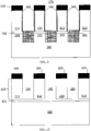
- the elevated structures 111, 112, 113, 114 are electrically isolated from each other by forming shallow trench isolation (STI) regions 130 in between the elevated structures 111-114 ( FIG.7 ), i.e. by partially filling the trenches 121, 122, 123 with an insulating material. This may be done by first completely filling the trenches 121, 122, 123 with an insulating material 131 ( Fig. 6 ), followed by a chemical-mechanical planarization step (CMP) to remove the excess insulating material on top of the hardmask layer.
- STI shallow trench isolation
- part of the insulating material 131 in the trenches is etched such that openings 141, 142, 143 remain in between the elevated structures 111, 112, 113, 114 ( Fig. 7 ).
- Etching the insulating material 131 may be done for example by dry or wet etching techniques.
- the insulating material 131 may comprise or consist of silicon oxide or any material known for a person skilled in the art for providing STI regions.
- the shallow trench isolation regions 130 are preferably deep enough, i.e. for example about 300 nm.
- the shallow trench isolation regions 130 should extend slightly, i.e.
- each of the isolation regions 130 is thus laterally in contact with the side wall of the base portions 100' and of the dielectric portions 101', and with (part of) the gate dielectric layer 160 of the elevated structures on either side of the trench in which the isolation region 130 is located.
- the elevated structures 111, 112, 113, 114 are formed of a monocrystalline semiconductor material, preferably monocrystalline Si.
- Either the entire hardmask layer or a part of it 103 preferably remains present during the whole manufacturing flow of the floating gate semiconductor device.
- the presence of the hardmask layer 103 may avoid excessive leakage at the corners of the cell (elevated structure).
- the hardmask layer may be removed after the step of providing the trenches, and thus the elevated structures.
- a gate dielectric layer 160 is provided on all the sidewall surfaces 180 of the elevated structures 111, 112, 113, 114 (see figures 7 and 8 ). If the hardmask is not present any more, or if the trenches 121-123 are formed by a technique that does not involve a hardmask, the gate dielectric layer 160 will also be provided at the top surface of the elevated structures 111, 112, 113, 114.
- the gate dielectric layer 160 at the sidewall surface 180 and optionally at the top surface of the elevated structures 111, 112, 113, 114 is formed by a thermal oxidation of the semiconducting material of the elevated structures 111, 112, 113, 114.
- the thermal oxidation may for example be performed by an in-situ steam generation (ISSG) oxidation step.
- the quality and scalability of the gate dielectric layer 160 can be improved significantly as this gives the opportunity to use thermal oxide grown on the monocrystalline floating gate.
- Such thermally grown oxide layers are thinner than the traditionally deposited ONO stacks on polycrystalline floating gates.
- the method of the invention is applicable on a monocrystalline layer 102, hence resulting in monocrystalline floating gate structures 102', hence providing the advantage of being able to produce thin lateral isolation layers ('lateral' meaning at the sidewalls of the fins), preferably having a thickness between 6nm and 8nm.
- the method of the invention therefore allows scaling down memory devices to the 1X generation node.
- the thermal oxidation leads to the formation of the gate dielectric layer 160 in such a way that said gate dielectric layer 160 overlaps with the isolation regions 130.
- this overlap extends down to the top surface of the dielectric portion 101'.
- this overlap may extend over a smaller distance so that the gate dielectric layer 160 does not extend down to the top surface of the dielectric portion 101', but extends to a height between said top surface and the top surface of the isolation region 130.
- the top of floating gate regions 102' may optionally be rounded, thereby forming rounded corners with a predetermined radius, for example with a radius of about 2nm, more preferably 4 nm. Corner rounding of the floating gate regions will avoid excessive current leakage.
- the thermal oxidation to form the gate dielectric 160 may itself cause a degree of corner rounding, e.g. up to a radius of about 2nm, at the top corners of the fins, whether or not the hardmask 103 is still present at the top of the fins.
- it is preferred to apply a suitable process before the formation of the gate dielectric 160 such as described for example in EP2073256 .
- a conductive layer 171 is provided over/on the elevated structures 111, 112, 113, 114 and the gate dielectric layer 160 ( FIG. 9 ).
- the cavities 141, 142, 143 in between the elevated structures 111, 112, 113, 114 are filled with said conductive material 171.
- the conductive material 171 is also provided on top of the fins. Further steps may then be done as known for a person skilled in the art such as for example source and drain (s/d) formation and implantation or doping of the fins.
- a floating gate semiconductor device is formed wherein part of the dielectric layer 101 is acting as the tunnel dielectric layer, part of the semiconductor layer 111, 112, 113, 114 is acting as the floating gate(s), the gate dielectric layer 160 is acting as the interpoly dielectric layer of prior art devices, and the conductive layer is acting as the control gate 171.
- a cell structure with monocrystalline floating gates and 6 nm to 8 nm of thermally grown SiO 2 gate dielectric is provided.
- This thin gate dielectric avoids the physical scaling barrier caused by the ONO thickness limitation.
- Simulations show that, down to the 12 nm node, such cells can be programmed without excessive gate dielectric leakage.
- the combination of modeling and experimental data indicates that 12 nm memory cells with 8 nm SiO 2 gate dielectric achieve 10 years data retention. Simulations predict further scaling potential towards 6nm gate dielectric in the 10 nm node.
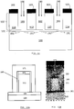
- FIG. 12A is a schematic representation of a semiconductor floating gate device whereas figure 12B shows a microscopy image of the semiconductor floating gate device.
- a SOI substrate (100-101-111) is shown with a Si (semiconductor base) layer 100, thereupon a tunnel oxide layer 101 (SOI buried oxide layer) with a thickness of about 10 nm.
- a floating gate region 111 is formed in the semiconductor layer.
- the floating gate region is a monocrystalline floating gate region with a thickness/height of about 75 nm and width of about 55 nm.
- a SiO 2 hardmask 103 is provided (before patterning the floating gate regions).
- the SiO 2 hardmask 103 is to avoid leakage at the top of the floating gate 111.
- the floating gate corners at the top may be rounded in order to avoid leakage, for example with a radius of 4 nm.
- the sidewalls of the monocrystalline floating gate region 111 have undergone a thermal oxidation step (more specifically an in-situ steam generation (ISSG) oxidation step) in order to form the SiO 2 gate dielectric layer with a width of about 6 to 8 nm wide. Thereafter a polysilicon control gate 171 with a thickness of about 25 nm is formed (by deposition and patterning) upon the floating gate/gate dielectric structure.
- ISSG in-situ steam generation
- Figure 13 shows simulation results for a floating gate device (as shown in Figure 12 ) of the positive flatband voltage V FB window as a function of the height of the floating gate with and without corner rounding for a gate dielectric layer of 6 nm or 8 nm. A difference of about 1.5V is seen between the results with or without corner rounding which proves the advantages of having corner rounded floating gate regions.
- the gate dielectric thickness is not critical towards programming performance within the studied range of 6 nm to 8 nm.
- NAND Flash can be scaled at least down to 12nm without major roadblocks (geometric scaling, parasitic interference, floating gate charge). Simulations and experimental results on test structures demonstrate that the aggressively scaled gate dielectric required for this still allows obtaining 10 years of data retention taking a small fraction of failing cells in account, still correctable by Error Checking and Correction algorithm (ECC).
- ECC Error Checking and Correction algorithm
Landscapes
- Engineering & Computer Science (AREA)
- Microelectronics & Electronic Packaging (AREA)
- Power Engineering (AREA)
- Physics & Mathematics (AREA)
- Ceramic Engineering (AREA)
- Condensed Matter Physics & Semiconductors (AREA)
- General Physics & Mathematics (AREA)
- Computer Hardware Design (AREA)
- Manufacturing & Machinery (AREA)
- Semiconductor Memories (AREA)
- Non-Volatile Memory (AREA)
- Electrodes Of Semiconductors (AREA)
Description
- The present invention is related to a floating gate semiconductor device, more particularly a monocrystalline floating gate semiconductor device.
- The present invention is also related to methods for manufacturing a floating gate semiconductor device, more particularly for manufacturing a monocrystalline floating gate semiconductor device.
- For NAND flash memory devices, the physical scaling as well as the electrical scaling has become more challenging with each technology node.
- In state-of-the-art NAND flash memory devices, the ONO (oxide-nitride-oxide) interpoly dielectric (IPD), which can more generally be referred to as the gate dielectric, runs along the sidewalls of the floating gate in order to provide a large capacitance between floating gate and control gate and therefore a large coupling ratio. As the IPD layer is present twice in one width defined by the pitch, in a floating gate flash device, scaling of thickness of the IPD layer becomes a limiting factor for flash scaling below a 2X generation technology node, which corresponds to a memory cell half-pitch between 20 nm and 29 nm included. To achieve good data retention, the physical thickness of the IPD layer is limited to about 12 to 15 nm using state-of-the art materials, which means already 24 to 30 nm pitch size at least, as it is still necessary to add the thickness of the floating gate and the control gate.
-
Figure 1 shows a schematic representation of a prior art floating gate memory device on asubstrate 1, comprisingfloating gate structures 2,isolation areas 3, interpolydielectric layer 4 wrapped around thefloating gate structures 2,tunnel oxide layers 5 andcontrol gate 6. It is seen that the scaling of the pitch P of floating gate memory device becomes a great challenge as it is necessary within the pitch P to have room for the floating gate (FG) 2, for an interpoly dielectric (IPD)layer 4, for a control gate (CG) 6 and again for an interpoly dielectric (IPD)layer 4. With the materials currently used for the IPD layer, i.e. ONO or AlO-based dielectric stack, the thickness of the IPD layer is limited to about 12 to 15 nm in order to achieve good data retention (i.e. about 10 years of data retention) for the memory device. When scaling to smaller thickness, the electrical properties of the materials currently used for the IPD layer are no longer sufficient since smaller thickness causes increased leakage and bad performance of the device. -
US2010/0248435 discloses a method of manufacturing a flash memory device. - There is a need for floating gate memory devices with a good data retention and electrical performance, which are scalable below 3X generation technology node, and even scalable below 2X generation technology node.
- The present invention is related to a method and device as disclosed in the appended claims. The invention is thus related to a method of manufacturing a floating gate semiconductor memory device according to
claim 1. - According to an embodiment, the step of providing isolation regions comprises the steps of filling said trenches with an insulating material, and partially removing said insulating material in each of said trenches so that a portion of said insulating material remains at the bottom of each of said trenches, forming said isolation regions in each of said trenches.
- The equivalent oxide thickness of the dielectric layer is preferably between 6nm and 10nm.
- According to an embodiment, besides the sidewall surfaces, also the top surface of the elevated structure(s) is oxidized.
- According to a preferred embodiment, said isolation regions at the bottom of each of said trenches are in contact with the semiconductor base portions, with the dielectric portions and with part of the gate dielectric layer of the elevated structures on either side of the trench, said isolation region extending above said dielectric portions. Preferably, the portion of the isolation regions extending above said dielectric portions has a height in the range of 5 to 20 nm.
- Said trenches may be formed by producing a patterned hardmask layer on top of the semiconductor-on-insulator substrate, and by etching said trenches in the areas not covered by said hardmask layer.
- According to an embodiment, said patterned hardmask layer remains on top of the elevated structure(s) and the conductive layer is provided on top of said hardmask layer.
- According to another embodiment, said hardmask layer is removed after the step of providing said trenches and prior to the step of providing the gate dielectric layer, the method further comprising the step of rounding the top corners of the elevated structure(s) after said removal of the hardmask layer and before said step of providing the gate dielectric layer .
- According to an embodiment of the method of the invention, said step of providing at least two trenches may comprise the following sub-steps :
- providing first trenches by etching through the top semiconductor layer thereby exposing the dielectric layer,
- further etching through the dielectric layer and partially through the base layer.
- In the latter embodiment, the method may further comprise the step, performed after the step of providing first trenches and before the step of further etching through the dielectric layer, of injecting dopant elements into the spaces formed between said first trenches.
- The thickness of said gate dielectric layer is preferably between 6nm and 8nm for a 2X generation technology node or lower. For a 1X generation technology node a smaller thickness may be preferred, i.e. smaller than 8 nm or even smaller than 6 nm.
- It is an advantage of method according to the invention that scaling of a semiconductor memory device can be done down to 1X generation technology node.
- Furthermore, it is an advantage of method according to the invention that more specifically for a floating gate semiconductor memory device, the gate dielectric layer may be scaled down to less than 12 nm.
- Furthermore, it is an advantage of method according to the invention that the aggressively scaled gate dielectric layer allows to obtain 10 years of data retention for the memory cell.
- Furthermore, it is an advantage of method according to the invention that a floating gate semiconductor memory device may be manufactured by using a simplified process flow. Thereby also manufacturing costs are reduced for manufacturing a floating gate semiconductor memory device.
-
Figure 1 illustrates a schematic representation of a non-volatile semiconductor memory device according to the prior art, more specifically a floating gate semiconductor memory device. -
Figure 2 to 11 illustrate different embodiments for methods for manufacturing a floating gate semiconductor device according to embodiments of the invention. -
Figure 12A and 12B illustrate an example of a floating gate semiconductor device according to embodiments of the invention. A schematic structure (12A) and a microscopic image (12B) are shown. -
Figure 13 shows simulation results of the positive VFB shift with and without corner rounding of the floating gate region manufactured according to embodiments of the present invention. -
Figure 14 illustrates experimental results of high-temperature data retention after 10 years for floating gate semiconductor device according to embodiments of the invention. - Any reference signs in the claims shall not be construed as limiting the scope.
- In the different drawings, the same reference signs refer to the same or analogous elements.
- One or more embodiments will now be described in detail with reference to the attached figures, while the invention is not limited thereto. The drawings described are only schematic and are non-limiting. In the drawings, the size of some of the elements may be exaggerated and not drawn on scale for illustrative purposes. Those skilled in the art can recognize numerous variations and modifications of this invention that are encompassed by its scope. Accordingly, the following description of certain inventive embodiments should not be deemed to limit the scope of the present invention.
- It is to be noticed that the term "comprising", used in the claims, should not be interpreted as being restricted to the means listed thereafter; it does not exclude other elements or steps. Thus, the scope of the expression "a device comprising means A and B" should not be limited to devices consisting only of components A and B. It means that with respect to the present invention, the only relevant components of the device are A and B.
- Reference throughout this specification to "one embodiment" or "an embodiment" means that a particular feature, structure or characteristic described in connection with the embodiment is included in at least one embodiment. Thus, appearances of the phrases "in one embodiment" or "in an embodiment" in various places throughout this specification are not necessarily all referring to the same embodiment, but may. Furthermore, the particular features, structures or characteristics may be combined in any suitable manner, as would be apparent to one of ordinary skill in the art from this disclosure, in one or more embodiments.
- Similarly it should be appreciated that in the description of exemplary embodiments, various features sometimes grouped together in a single embodiment, figure, or description thereof for the purpose of streamlining the disclosure and aiding in the understanding of one or more of the various features. This method of disclosure, however, is not to be interpreted as reflecting an intention that the claimed invention requires more features than are expressly recited in each claim. Rather, as the following claims reflect, inventive aspects lie in less than all features of a single foregoing disclosed embodiment. Thus, the claims following the detailed description are hereby expressly incorporated into this detailed description, with each claim standing on its own as encompassing one or more separate embodiments of this invention.
- Furthermore, while some embodiments described herein include some but not other features included in other embodiments, combinations of features of different embodiments are meant to be within the scope of the invention, and form different embodiments, as would be understood by those in the art. For example, in the following claims, any of the claimed embodiments can be used in any combination.
- In the description provided herein, numerous specific details are set forth. However, it is understood that embodiments of the invention may be practiced without these specific details. In other instances, well-known methods, structures and techniques have not been shown in detail in order not to obscure an understanding of this description.
- Embodiments for manufacturing a floating gate semiconductor memory device according to the invention will now be described in more detail with reference to
figure 2 to figure 11 . - The starting material in the method of the invention is a semiconductor-on-insulator substrate 1000 (
Fig. 2 ). The semiconductor-on-insulator substrate comprises an insulatinglayer 101, which is a dielectric layer sandwiched in between asemiconductor base layer 100 and asemiconductor top layer 102. Thesemiconductor top layer 102 comprises or consists of a monocrystalline semiconducting material. For example, the semiconductor-on-insulator substrate 1000 may be an SOI substrate, i.e. a monocrystalline silicon (Si)top layer 102 on and in contact with a buried silicon oxide layer 101 (known as 'box' layer), the buried silicon oxide layer on and in contact with asilicon base layer 100. - The
dielectric layer 101 is preferably an ultrathin layer, which means that the equivalent oxide thickness of thedielectric layer 101 is preferably smaller than 10nm, more preferably between 6nm and 10nm. - According to one embodiment, at least two
trenches FIG. 5 ), thetrenches semiconductor base layer 100, thereby forming at least oneelevated structure semiconductor top portion 102' (part of the semiconductor top layer 102) on and in contact with an dielectric portion 101' (part of the dielectric layer 101) on and in contact with a semiconductor base portion 100' (part of the semiconductor base layer 100). Thesemiconductor top portion 102' of the elevated structures will serve as the floating gate of the semiconductor memory device. The dielectric portion 101' of the elevated structures will act as the tunnel dielectric layer of the semiconductor memory device. - Forming the at least two trenches 121-123 (and thus the elevated structures 111-114) may be done using conventional techniques known for a person skilled in the art, for example by using lithographic techniques as explained further.
- In the embodiment shown, a
hardmask layer 103 is provided on top of the semiconductor substrate 1000 (Fig. 3 ). Thehardmask layer 103 may for example be a nitride layer, an oxide layer or a combination thereof. - Next the
hardmask layer 103 is patterned (Fig. 4 ). Using lithographic techniques, a photoresist material (not shown) may be applied on top of thehardmask layer 103, exposed, developed and etched. Next theunderlying hardmask layer 103 may be etched using the patterned photoresist material as a mask. As a result thehardmask layer 103 is patterned, i.e. openings are etched in the hardmask layer thereby exposing theunderlying semiconductor substrate 1000. - By using the patterned
hardmask layer 103 as a mask, theunderlying semiconductor substrate 1000 may be etched (Fig. 5 ), thereby forming a series of openings (trenches) 121, 122, 123 in thesemiconductor substrate 1000 or in other words : thereby forming a series ofelevated structures - According to an alternative embodiment, forming the at least two trenches is done in two steps so that in a first etching step
first trenches Fig. 10 ) and in a second etching step thefinal trenches Fig. 5 ) by etching part of thedielectric layer 101 in between the elevated structures already formed and by etching part of thesemiconductor substrate 100 further on. In between the first and the second etching step,dopant atoms 190 may be implanted into thesubstrate 100 and diffused under theelevated structures Fig. 11 ). In this way,channel regions 191 in the substrate are formed under the elevated structures, e.g. by a thermal anneal, the specifics of which are known per se to the skilled person.. - When the doping method is perpendicular to the substrate surface (in other words perpendicular to the top surface of the elevated structures) and the top surface of the elevated structures is covered with a
hard mask layer 103, the elevated structures will not be doped during this doping step or at least will only receive a very small (negligible) amount of dopants. Other methods of doping the channel region in the substrate could also be foreseen as known by a person skilled in the art. When the trenches 121-123 as shown infigure 5 are formed in one etching step, the method may comprise a step of implanting dopant elements by implanting said elements through the side walls of the elevated structures 111-114, again to formchannel regions 191 underneath the dielectric portions 101'. Sidewall doping as such is equally known to the skilled person. - The elevated structures 111-114 may also be formed for example by using spacer-defined patterning as known for a person skilled in the art.
- Depending on the applications and technology node for which the resulting semiconductor devices will be used, the dimensions of the elevated structures may differ. Preferably, for floating gate memory device applications, the width W1 of the trenches (see
FIG. 5 ) is in the range of 14 nm to 25 nm, the width W2 of the elevated structures in the range of 3 nm to 30 nm, the depth D1 of the trenches is in the range of 230nm to 370nm, whereby the depth D2 of part of the trenches underneath thedielectric layer 101 is in the range of 200nm to 300nm. - In a next step the
elevated structures regions 130 in between the elevated structures 111-114 (FIG.7 ), i.e. by partially filling thetrenches trenches Fig. 6 ), followed by a chemical-mechanical planarization step (CMP) to remove the excess insulating material on top of the hardmask layer. Next, part of the insulatingmaterial 131 in the trenches is etched such thatopenings elevated structures Fig. 7 ). Etching the insulatingmaterial 131 may be done for example by dry or wet etching techniques. The insulatingmaterial 131 may comprise or consist of silicon oxide or any material known for a person skilled in the art for providing STI regions. To ensure a good electrical isolation between the fins, the shallowtrench isolation regions 130 are preferably deep enough, i.e. for example about 300 nm. The shallowtrench isolation regions 130 should extend slightly, i.e. preferably in the range of 5 to 20 nm above the tunnel dielectric portions 101' in order to avoid leakage from the floatinggate channel layer 191 in the control gate layer 171 (FIG. 9 ). According to the latter embodiment, each of theisolation regions 130 is thus laterally in contact with the side wall of the base portions 100' and of the dielectric portions 101', and with (part of) thegate dielectric layer 160 of the elevated structures on either side of the trench in which theisolation region 130 is located. - The
elevated structures - Either the entire hardmask layer or a part of it 103 preferably remains present during the whole manufacturing flow of the floating gate semiconductor device. The presence of the
hardmask layer 103 may avoid excessive leakage at the corners of the cell (elevated structure). Alternatively the hardmask layer may be removed after the step of providing the trenches, and thus the elevated structures. - After the formation of the shallow
trench isolation regions 130, agate dielectric layer 160 is provided on all the sidewall surfaces 180 of theelevated structures figures 7 and 8 ). If the hardmask is not present any more, or if the trenches 121-123 are formed by a technique that does not involve a hardmask, thegate dielectric layer 160 will also be provided at the top surface of theelevated structures - According to the invention, the
gate dielectric layer 160 at thesidewall surface 180 and optionally at the top surface of theelevated structures elevated structures - By using a monocrystalline semiconductor material (e.g. monocrystalline silicon) for the
top portions 102' of the elevated structures (i.e. the floating gates), the quality and scalability of thegate dielectric layer 160 can be improved significantly as this gives the opportunity to use thermal oxide grown on the monocrystalline floating gate. - Such thermally grown oxide layers are thinner than the traditionally deposited ONO stacks on polycrystalline floating gates. The method of the invention is applicable on a
monocrystalline layer 102, hence resulting in monocrystalline floatinggate structures 102', hence providing the advantage of being able to produce thin lateral isolation layers ('lateral' meaning at the sidewalls of the fins), preferably having a thickness between 6nm and 8nm. The method of the invention therefore allows scaling down memory devices to the 1X generation node. - As shown in
figure 8 , the thermal oxidation leads to the formation of thegate dielectric layer 160 in such a way that saidgate dielectric layer 160 overlaps with theisolation regions 130. In the embodiment shown, this overlap extends down to the top surface of the dielectric portion 101'. However this overlap may extend over a smaller distance so that thegate dielectric layer 160 does not extend down to the top surface of the dielectric portion 101', but extends to a height between said top surface and the top surface of theisolation region 130. - The top of floating
gate regions 102' may optionally be rounded, thereby forming rounded corners with a predetermined radius, for example with a radius of about 2nm, more preferably 4 nm. Corner rounding of the floating gate regions will avoid excessive current leakage. The thermal oxidation to form thegate dielectric 160 may itself cause a degree of corner rounding, e.g. up to a radius of about 2nm, at the top corners of the fins, whether or not thehardmask 103 is still present at the top of the fins. To obtain rounded corners with a radius higher than 2nm, it is preferred to apply a suitable process before the formation of thegate dielectric 160, such as described for example inEP2073256 . - After the formation of the
gate dielectric 160, aconductive layer 171 is provided over/on theelevated structures FIG. 9 ). Thecavities elevated structures conductive material 171. Theconductive material 171 is also provided on top of the fins. Further steps may then be done as known for a person skilled in the art such as for example source and drain (s/d) formation and implantation or doping of the fins. - As such a floating gate semiconductor device is formed wherein part of the
dielectric layer 101 is acting as the tunnel dielectric layer, part of thesemiconductor layer gate dielectric layer 160 is acting as the interpoly dielectric layer of prior art devices, and the conductive layer is acting as thecontrol gate 171. - An example of a monocrystalline floating gate device and its electrical characteristics according to embodiments are now described.
- As an example, a cell structure with monocrystalline floating gates and 6 nm to 8 nm of thermally grown SiO2 gate dielectric is provided. This thin gate dielectric avoids the physical scaling barrier caused by the ONO thickness limitation. Simulations show that, down to the 12 nm node, such cells can be programmed without excessive gate dielectric leakage. The combination of modeling and experimental data indicates that 12 nm memory cells with 8 nm SiO2 gate dielectric achieve 10 years data retention. Simulations predict further scaling potential towards 6nm gate dielectric in the 10 nm node.
- A cross-section of the proposed cell structure is shown in
figure 12A and 12B. Figure 12A is a schematic representation of a semiconductor floating gate device whereasfigure 12B shows a microscopy image of the semiconductor floating gate device. A SOI substrate (100-101-111) is shown with a Si (semiconductor base)layer 100, thereupon a tunnel oxide layer 101 (SOI buried oxide layer) with a thickness of about 10 nm. In the semiconductor layer a floatinggate region 111 is formed. The floating gate region is a monocrystalline floating gate region with a thickness/height of about 75 nm and width of about 55 nm. On the floating gate region 111 a SiO2 hardmask 103 is provided (before patterning the floating gate regions). The SiO2 hardmask 103 is to avoid leakage at the top of the floatinggate 111. The floating gate corners at the top may be rounded in order to avoid leakage, for example with a radius of 4 nm. The sidewalls of the monocrystalline floatinggate region 111 have undergone a thermal oxidation step (more specifically an in-situ steam generation (ISSG) oxidation step) in order to form the SiO2 gate dielectric layer with a width of about 6 to 8 nm wide. Thereafter apolysilicon control gate 171 with a thickness of about 25 nm is formed (by deposition and patterning) upon the floating gate/gate dielectric structure. - In order to estimate programming performance and cell-to-cell interference, simulations of cell coupling in a dense array are performed using Raphael RC3. Programming and gate dielectric leakage are obtained using the nonlocal tunneling model in Sentaurus device on single memory cells in combination with the coupling ratios as obtained from RC3. Programming saturation is defined as the threshold voltage (Vth) shift for which the gate dielectric leakage is equal to the tunnel oxide current with a floating gate voltage VFG = 8.5V. Data retention is investigated both by using a percolation model and by measurements on dedicated floating gate test structures.
- It is shown in
Figure 13 that both the height and corner rounding of the floating gate region strongly impacts programming saturation for a single cell. As noted above, the thermal oxidation to form the gate dielectric will normally cause a limited corner rounding, so the case without corner rounding is primarily to be regarded as theoretical.Figure 13 shows simulation results for a floating gate device (as shown inFigure 12 ) of the positive flatband voltage VFB window as a function of the height of the floating gate with and without corner rounding for a gate dielectric layer of 6 nm or 8 nm. A difference of about 1.5V is seen between the results with or without corner rounding which proves the advantages of having corner rounded floating gate regions. However the gate dielectric thickness is not critical towards programming performance within the studied range of 6 nm to 8 nm. - Also high-temperature data retention has been measured on dedicated test structures (as shown in
Figure 12B ) comprising a large number of monocrystalline floating gate stripes, which are elongate floating gate test structures. It can clearly be seen inFigure 14 that the quality of the thin SiO2 hardmask (capping) layer grown on the floating gate is very good, resulting in a small threshold voltage (Vth) after a bake of more than 40 hours at a temperature of 200 degrees Celsius. Fill lines show the results for a monocrystalline floating gate, whereas dashed lines show the results for a polycrystalline floating gate. Results for 6 nm gate dielectric and 8 nm gate dielectric are shown. - It is an advantage of embodiments of certain inventive aspects that a monocrystalline floating gate structure with aggressively scaled thermal SiO2 gate dielectric for ultimate floating gate NAND cell scaling may be provided. With this structure, NAND Flash can be scaled at least down to 12nm without major roadblocks (geometric scaling, parasitic interference, floating gate charge). Simulations and experimental results on test structures demonstrate that the aggressively scaled gate dielectric required for this still allows obtaining 10 years of data retention taking a small fraction of failing cells in account, still correctable by Error Checking and Correction algorithm (ECC).
Claims (11)
- A method of manufacturing a floating gate semiconductor memory device, the method comprising:- providing a semiconductor-on-insulator substrate (1000), the semiconductor-on-insulator substrate comprising :- a semiconductor base layer (100),- on and in contact with said base layer : a dielectric layer (101),- on and in contact with said dielectric layer : a monocrystalline semiconductor top layer (102),- providing at least two trenches (121,122,123) in the semiconductor-on-insulator substrate (1000), the trenches extending through the semiconductor top layer (102), the dielectric layer (101) and partially through the semiconductor base layer (100), thereby forming at least one elevated structure (111-114), the elevated structure comprising :- a base portion (100'), which is part of the base substrate (100),- on and in contact with said base portion : a dielectric portion (101'), which is part of the dielectric layer (101),- on and in contact with said dielectric portion, a monocrystalline semiconductor top portion (102'), which is part of the semiconductor top layer (102);- providing isolation regions (130) at the bottom of each of said trenches;- providing a gate dielectric layer (160) at least at the sidewall surfaces of the elevated structure(s), by a thermal oxidation of the sidewall surfaces (180) of the top portion (102') of the elevated structure(s) (111-114);- providing a conductive layer (171) over the elevated structure(s) and the gate dielectric layer (160), to thereby form at least one floating gate semiconductor memory device, said gate dielectric region acting as the interpoly dielectric layer, said dielectric portion (101') acting as the tunnel dielectric layer, said semiconductor top portion (102') acting as the floating gate and said conductive layer (171) acting as the control gate.
- Method according to claim 1, wherein the step of providing isolation regions (130) comprises the steps of filling said trenches with an insulating material (131), and partially removing said insulating material (131) in each of said trenches so that a portion (130) of said insulating material remains at the bottom of each of said trenches, forming said isolation regions (130) in each of said trenches.
- Method according to claim 1 or 2 wherein the equivalent oxide thickness of the dielectric layer (101) is between 6nm and 10nm.
- Method according to any one of claims 1 to 3, wherein besides the sidewall surfaces (180), also the top surface of the elevated structure(s) (111-114) is oxidized.
- Method according to any one of claims 1 to 4 wherein said isolation regions (130) at the bottom of each of said trenches are in contact with the semiconductor base portions (100'), with the dielectric portions (101') and with part of the gate dielectric layer (160) of the elevated structures on either side of the trench, said isolation region (130) extending above said dielectric portions (101').
- Method according to any one of the preceding claims, wherein said trenches (121-123) are formed by producing a patterned hardmask layer (103) on top of the semiconductor-on-insulator substrate (1000), and by etching said trenches in the areas not covered by said hardmask layer (103).
- Method according to claim 6, wherein said patterned hardmask layer (103) remains on top of the elevated structure(s) (111-114) and the conductive layer (171) is provided on top of said hardmask layer (103).
- Method according to claim 6, wherein said hardmask layer (103) is removed after the step of providing said trenches (121-123) and prior to the step of providing the gate dielectric layer (160), the method further comprising the step of rounding the top corners of the elevated structure(s) (111-114) after said removal of the hardmask layer (103) and before said step of providing the gate dielectric layer (160).
- Method according to any one of claims 6 to 8, wherein said step of providing at least two trenches (121-123) comprises the following sub-steps :- providing first trenches (181-183) by etching through the top semiconductor layer (102) thereby exposing the dielectric layer (101),- further etching through the dielectric layer (101) and partially through the base layer (100).
- Method according to claim 9, further comprising the step, performed after the step of providing first trenches and before the step of further etching through the dielectric layer (101), of injecting dopant elements (190) into the spaces formed between said first trenches (181-183).
- Method according to any one of claims 1 to 10, wherein the thickness of said gate dielectric layer (160) is between 6nm and 8nm.
Priority Applications (2)
| Application Number | Priority Date | Filing Date | Title |
|---|---|---|---|
| JP2012046149A JP5788346B2 (en) | 2011-03-03 | 2012-03-02 | Floating gate semiconductor memory device and method of manufacturing such a device |
| US13/410,843 US8652902B2 (en) | 2011-03-03 | 2012-03-02 | Floating gate semiconductor memory device and method for producing such a device |
Applications Claiming Priority (1)
| Application Number | Priority Date | Filing Date | Title |
|---|---|---|---|
| US201161448828P | 2011-03-03 | 2011-03-03 |
Publications (2)
| Publication Number | Publication Date |
|---|---|
| EP2495762A1 EP2495762A1 (en) | 2012-09-05 |
| EP2495762B1 true EP2495762B1 (en) | 2017-11-01 |
Family
ID=44675408
Family Applications (1)
| Application Number | Title | Priority Date | Filing Date |
|---|---|---|---|
| EP11075160.9A Not-in-force EP2495762B1 (en) | 2011-03-03 | 2011-07-06 | Method for producing a floating gate semiconductor memory device |
Country Status (3)
| Country | Link |
|---|---|
| US (1) | US8652902B2 (en) |
| EP (1) | EP2495762B1 (en) |
| JP (1) | JP5788346B2 (en) |
Families Citing this family (2)
| Publication number | Priority date | Publication date | Assignee | Title |
|---|---|---|---|---|
| TWI473211B (en) * | 2012-10-19 | 2015-02-11 | Inotera Memories Inc | Random access memory and manufacturing method for node thereof |
| US8963228B2 (en) * | 2013-04-18 | 2015-02-24 | International Business Machines Corporation | Non-volatile memory device integrated with CMOS SOI FET on a single chip |
Family Cites Families (23)
| Publication number | Priority date | Publication date | Assignee | Title |
|---|---|---|---|---|
| JPS5931231B2 (en) | 1980-01-31 | 1984-07-31 | 工業技術院長 | Floating gate non-volatile semiconductor memory |
| JP2633541B2 (en) | 1987-01-07 | 1997-07-23 | 株式会社東芝 | Method for manufacturing semiconductor memory device |
| JPH01255271A (en) | 1988-04-05 | 1989-10-12 | Nec Corp | Semiconductor integrated circuit device |
| JP2668707B2 (en) | 1988-06-07 | 1997-10-27 | セイコー電子工業株式会社 | Manufacturing method of semiconductor nonvolatile memory |
| US5387540A (en) * | 1993-09-30 | 1995-02-07 | Motorola Inc. | Method of forming trench isolation structure in an integrated circuit |
| JPH08125037A (en) | 1994-10-24 | 1996-05-17 | Hitachi Ltd | Semiconductor device and its manufacture |
| JP3422593B2 (en) * | 1995-04-07 | 2003-06-30 | 三菱電機株式会社 | Method for manufacturing semiconductor device |
| US20030170964A1 (en) * | 1996-10-02 | 2003-09-11 | Micron Technology, Inc. | Oxidation of ion implanted semiconductors |
| JPH11103033A (en) * | 1997-09-29 | 1999-04-13 | Sony Corp | Manufacture of nonvolatile semiconductor memory device |
| US6300219B1 (en) * | 1999-08-30 | 2001-10-09 | Micron Technology, Inc. | Method of forming trench isolation regions |
| US6352921B1 (en) * | 2000-07-19 | 2002-03-05 | Chartered Semiconductor Manufacturing Ltd. | Use of boron carbide as an etch-stop and barrier layer for copper dual damascene metallization |
| US6881645B2 (en) * | 2000-08-17 | 2005-04-19 | Samsung Electronics Co., Ltd. | Method of preventing semiconductor layers from bending and semiconductor device formed thereby |
| US6897514B2 (en) * | 2001-03-28 | 2005-05-24 | Matrix Semiconductor, Inc. | Two mask floating gate EEPROM and method of making |
| US6734063B2 (en) * | 2002-07-22 | 2004-05-11 | Infineon Technologies Ag | Non-volatile memory cell and fabrication method |
| US7390710B2 (en) * | 2004-09-02 | 2008-06-24 | Micron Technology, Inc. | Protection of tunnel dielectric using epitaxial silicon |
| JP2007207815A (en) * | 2006-01-31 | 2007-08-16 | Seiko Epson Corp | Semiconductor device, and method of manufacturing semiconductor device |
| US7452766B2 (en) * | 2006-08-31 | 2008-11-18 | Micron Technology, Inc. | Finned memory cells and the fabrication thereof |
| JP2009141277A (en) * | 2007-12-10 | 2009-06-25 | Toshiba Corp | Semiconductor device and its manufacturing method |
| EP2073256A1 (en) | 2007-12-20 | 2009-06-24 | Interuniversitair Microelektronica Centrum vzw ( IMEC) | Method for fabricating a semiconductor device and the semiconductor device made thereof |
| KR101024336B1 (en) * | 2009-02-13 | 2011-03-23 | 매그나칩 반도체 유한회사 | Nonvolatile memory cell and fabrication method thereof |
| JP4929300B2 (en) * | 2009-02-25 | 2012-05-09 | 株式会社東芝 | Multi-dot flash memory and manufacturing method thereof |
| JP5595481B2 (en) * | 2009-03-31 | 2014-09-24 | アプライド マテリアルズ インコーポレイテッド | Method of selective nitrogenation |
| US7947589B2 (en) * | 2009-09-02 | 2011-05-24 | Freescale Semiconductor, Inc. | FinFET formation with a thermal oxide spacer hard mask formed from crystalline silicon layer |
-
2011
- 2011-07-06 EP EP11075160.9A patent/EP2495762B1/en not_active Not-in-force
-
2012
- 2012-03-02 JP JP2012046149A patent/JP5788346B2/en not_active Expired - Fee Related
- 2012-03-02 US US13/410,843 patent/US8652902B2/en not_active Expired - Fee Related
Non-Patent Citations (1)
| Title |
|---|
| None * |
Also Published As
| Publication number | Publication date |
|---|---|
| US20120223378A1 (en) | 2012-09-06 |
| JP5788346B2 (en) | 2015-09-30 |
| EP2495762A1 (en) | 2012-09-05 |
| JP2012186474A (en) | 2012-09-27 |
| US8652902B2 (en) | 2014-02-18 |
Similar Documents
| Publication | Publication Date | Title |
|---|---|---|
| US20130341701A1 (en) | Vertical Semiconductor Memory Device and Manufacturing Method Thereof | |
| US7696554B2 (en) | Flash memory device | |
| EP2455967B1 (en) | A method for forming a buried dielectric layer underneath a semiconductor fin | |
| US8803218B2 (en) | Nonvolatile memory device and method for fabricating the same | |
| CN105826273A (en) | Flash memory device and manufacturing method thereof | |
| CN106129008A (en) | The forming method of flash memory | |
| JP2006319202A (en) | Semiconductor integrated circuit device and its manufacturing method | |
| JP2006049915A (en) | Nonvolatile memory device and its manufacturing method | |
| KR20080001266A (en) | Method of manufacturing a flash memory device | |
| US8575676B2 (en) | Semiconductor storage device and method for manufacturing the same | |
| EP2495762B1 (en) | Method for producing a floating gate semiconductor memory device | |
| US9105738B2 (en) | Semiconductor device and method of manufacturing the same | |
| CN106328656B (en) | A kind of adjustable control grid increase the process of ILD filling window | |
| JP2009188204A (en) | Flash memory and its production method | |
| CN112420730A (en) | Semiconductor process and semiconductor structure | |
| KR100910524B1 (en) | Flash memory device and method of fabricating the same | |
| CN109935592B (en) | Memory and preparation method thereof | |
| CN110021604B (en) | Memory and preparation method thereof | |
| KR101166810B1 (en) | Non volatile memory device and method for manufacturing the same | |
| KR20080060347A (en) | Method for manufacturing non-volatile memory device | |
| KR100695430B1 (en) | Method for forming floating gate in nonvolatile memory device | |
| US20150093863A1 (en) | Method of making a floating gate non-volatile memory (nvm) with breakdown prevention | |
| JP2014135514A (en) | Semiconductor memory device | |
| KR20080036859A (en) | Method for fabricating flash memory device | |
| JP2011114007A (en) | Semiconductor device and method for manufacturing the same |
Legal Events
| Date | Code | Title | Description |
|---|---|---|---|
| PUAI | Public reference made under article 153(3) epc to a published international application that has entered the european phase |
Free format text: ORIGINAL CODE: 0009012 |
|
| AK | Designated contracting states |
Kind code of ref document: A1 Designated state(s): AL AT BE BG CH CY CZ DE DK EE ES FI FR GB GR HR HU IE IS IT LI LT LU LV MC MK MT NL NO PL PT RO RS SE SI SK SM TR |
|
| AX | Request for extension of the european patent |
Extension state: BA ME |
|
| RAP3 | Party data changed (applicant data changed or rights of an application transferred) |
Owner name: IMEC VZW |
|
| 17P | Request for examination filed |
Effective date: 20130301 |
|
| 17Q | First examination report despatched |
Effective date: 20140703 |
|
| REG | Reference to a national code |
Ref country code: DE Ref legal event code: R079 Ref document number: 602011042832 Country of ref document: DE Free format text: PREVIOUS MAIN CLASS: H01L0027115000 Ipc: H01L0029660000 |
|
| GRAP | Despatch of communication of intention to grant a patent |
Free format text: ORIGINAL CODE: EPIDOSNIGR1 |
|
| RIC1 | Information provided on ipc code assigned before grant |
Ipc: H01L 29/66 20060101AFI20170627BHEP Ipc: H01L 29/423 20060101ALI20170627BHEP |
|
| INTG | Intention to grant announced |
Effective date: 20170719 |
|
| GRAS | Grant fee paid |
Free format text: ORIGINAL CODE: EPIDOSNIGR3 |
|
| GRAA | (expected) grant |
Free format text: ORIGINAL CODE: 0009210 |
|
| AK | Designated contracting states |
Kind code of ref document: B1 Designated state(s): AL AT BE BG CH CY CZ DE DK EE ES FI FR GB GR HR HU IE IS IT LI LT LU LV MC MK MT NL NO PL PT RO RS SE SI SK SM TR |
|
| REG | Reference to a national code |
Ref country code: GB Ref legal event code: FG4D |
|
| REG | Reference to a national code |
Ref country code: CH Ref legal event code: EP Ref country code: AT Ref legal event code: REF Ref document number: 942828 Country of ref document: AT Kind code of ref document: T Effective date: 20171115 |
|
| REG | Reference to a national code |
Ref country code: IE Ref legal event code: FG4D |
|
| REG | Reference to a national code |
Ref country code: DE Ref legal event code: R096 Ref document number: 602011042832 Country of ref document: DE |
|
| REG | Reference to a national code |
Ref country code: NL Ref legal event code: MP Effective date: 20171101 |
|
| REG | Reference to a national code |
Ref country code: LT Ref legal event code: MG4D |
|
| REG | Reference to a national code |
Ref country code: AT Ref legal event code: MK05 Ref document number: 942828 Country of ref document: AT Kind code of ref document: T Effective date: 20171101 |
|
| PG25 | Lapsed in a contracting state [announced via postgrant information from national office to epo] |
Ref country code: ES Free format text: LAPSE BECAUSE OF FAILURE TO SUBMIT A TRANSLATION OF THE DESCRIPTION OR TO PAY THE FEE WITHIN THE PRESCRIBED TIME-LIMIT Effective date: 20171101 Ref country code: NL Free format text: LAPSE BECAUSE OF FAILURE TO SUBMIT A TRANSLATION OF THE DESCRIPTION OR TO PAY THE FEE WITHIN THE PRESCRIBED TIME-LIMIT Effective date: 20171101 Ref country code: SE Free format text: LAPSE BECAUSE OF FAILURE TO SUBMIT A TRANSLATION OF THE DESCRIPTION OR TO PAY THE FEE WITHIN THE PRESCRIBED TIME-LIMIT Effective date: 20171101 Ref country code: LT Free format text: LAPSE BECAUSE OF FAILURE TO SUBMIT A TRANSLATION OF THE DESCRIPTION OR TO PAY THE FEE WITHIN THE PRESCRIBED TIME-LIMIT Effective date: 20171101 Ref country code: NO Free format text: LAPSE BECAUSE OF FAILURE TO SUBMIT A TRANSLATION OF THE DESCRIPTION OR TO PAY THE FEE WITHIN THE PRESCRIBED TIME-LIMIT Effective date: 20180201 Ref country code: FI Free format text: LAPSE BECAUSE OF FAILURE TO SUBMIT A TRANSLATION OF THE DESCRIPTION OR TO PAY THE FEE WITHIN THE PRESCRIBED TIME-LIMIT Effective date: 20171101 |
|
| PG25 | Lapsed in a contracting state [announced via postgrant information from national office to epo] |
Ref country code: BG Free format text: LAPSE BECAUSE OF FAILURE TO SUBMIT A TRANSLATION OF THE DESCRIPTION OR TO PAY THE FEE WITHIN THE PRESCRIBED TIME-LIMIT Effective date: 20180201 Ref country code: IS Free format text: LAPSE BECAUSE OF FAILURE TO SUBMIT A TRANSLATION OF THE DESCRIPTION OR TO PAY THE FEE WITHIN THE PRESCRIBED TIME-LIMIT Effective date: 20180301 Ref country code: GR Free format text: LAPSE BECAUSE OF FAILURE TO SUBMIT A TRANSLATION OF THE DESCRIPTION OR TO PAY THE FEE WITHIN THE PRESCRIBED TIME-LIMIT Effective date: 20180202 Ref country code: HR Free format text: LAPSE BECAUSE OF FAILURE TO SUBMIT A TRANSLATION OF THE DESCRIPTION OR TO PAY THE FEE WITHIN THE PRESCRIBED TIME-LIMIT Effective date: 20171101 Ref country code: LV Free format text: LAPSE BECAUSE OF FAILURE TO SUBMIT A TRANSLATION OF THE DESCRIPTION OR TO PAY THE FEE WITHIN THE PRESCRIBED TIME-LIMIT Effective date: 20171101 Ref country code: RS Free format text: LAPSE BECAUSE OF FAILURE TO SUBMIT A TRANSLATION OF THE DESCRIPTION OR TO PAY THE FEE WITHIN THE PRESCRIBED TIME-LIMIT Effective date: 20171101 Ref country code: AT Free format text: LAPSE BECAUSE OF FAILURE TO SUBMIT A TRANSLATION OF THE DESCRIPTION OR TO PAY THE FEE WITHIN THE PRESCRIBED TIME-LIMIT Effective date: 20171101 |
|
| REG | Reference to a national code |
Ref country code: FR Ref legal event code: PLFP Year of fee payment: 8 |
|
| PG25 | Lapsed in a contracting state [announced via postgrant information from national office to epo] |
Ref country code: DK Free format text: LAPSE BECAUSE OF FAILURE TO SUBMIT A TRANSLATION OF THE DESCRIPTION OR TO PAY THE FEE WITHIN THE PRESCRIBED TIME-LIMIT Effective date: 20171101 Ref country code: EE Free format text: LAPSE BECAUSE OF FAILURE TO SUBMIT A TRANSLATION OF THE DESCRIPTION OR TO PAY THE FEE WITHIN THE PRESCRIBED TIME-LIMIT Effective date: 20171101 Ref country code: CY Free format text: LAPSE BECAUSE OF FAILURE TO SUBMIT A TRANSLATION OF THE DESCRIPTION OR TO PAY THE FEE WITHIN THE PRESCRIBED TIME-LIMIT Effective date: 20171101 Ref country code: SK Free format text: LAPSE BECAUSE OF FAILURE TO SUBMIT A TRANSLATION OF THE DESCRIPTION OR TO PAY THE FEE WITHIN THE PRESCRIBED TIME-LIMIT Effective date: 20171101 Ref country code: CZ Free format text: LAPSE BECAUSE OF FAILURE TO SUBMIT A TRANSLATION OF THE DESCRIPTION OR TO PAY THE FEE WITHIN THE PRESCRIBED TIME-LIMIT Effective date: 20171101 |
|
| REG | Reference to a national code |
Ref country code: DE Ref legal event code: R097 Ref document number: 602011042832 Country of ref document: DE |
|
| PG25 | Lapsed in a contracting state [announced via postgrant information from national office to epo] |
Ref country code: PL Free format text: LAPSE BECAUSE OF FAILURE TO SUBMIT A TRANSLATION OF THE DESCRIPTION OR TO PAY THE FEE WITHIN THE PRESCRIBED TIME-LIMIT Effective date: 20171101 Ref country code: SM Free format text: LAPSE BECAUSE OF FAILURE TO SUBMIT A TRANSLATION OF THE DESCRIPTION OR TO PAY THE FEE WITHIN THE PRESCRIBED TIME-LIMIT Effective date: 20171101 Ref country code: IT Free format text: LAPSE BECAUSE OF FAILURE TO SUBMIT A TRANSLATION OF THE DESCRIPTION OR TO PAY THE FEE WITHIN THE PRESCRIBED TIME-LIMIT Effective date: 20171101 Ref country code: RO Free format text: LAPSE BECAUSE OF FAILURE TO SUBMIT A TRANSLATION OF THE DESCRIPTION OR TO PAY THE FEE WITHIN THE PRESCRIBED TIME-LIMIT Effective date: 20171101 |
|
| PLBE | No opposition filed within time limit |
Free format text: ORIGINAL CODE: 0009261 |
|
| STAA | Information on the status of an ep patent application or granted ep patent |
Free format text: STATUS: NO OPPOSITION FILED WITHIN TIME LIMIT |
|
| 26N | No opposition filed |
Effective date: 20180802 |
|
| PG25 | Lapsed in a contracting state [announced via postgrant information from national office to epo] |
Ref country code: SI Free format text: LAPSE BECAUSE OF FAILURE TO SUBMIT A TRANSLATION OF THE DESCRIPTION OR TO PAY THE FEE WITHIN THE PRESCRIBED TIME-LIMIT Effective date: 20171101 |
|
| REG | Reference to a national code |
Ref country code: CH Ref legal event code: PL |
|
| GBPC | Gb: european patent ceased through non-payment of renewal fee |
Effective date: 20180706 |
|
| PG25 | Lapsed in a contracting state [announced via postgrant information from national office to epo] |
Ref country code: MC Free format text: LAPSE BECAUSE OF FAILURE TO SUBMIT A TRANSLATION OF THE DESCRIPTION OR TO PAY THE FEE WITHIN THE PRESCRIBED TIME-LIMIT Effective date: 20171101 Ref country code: LU Free format text: LAPSE BECAUSE OF NON-PAYMENT OF DUE FEES Effective date: 20180706 |
|
| REG | Reference to a national code |
Ref country code: BE Ref legal event code: MM Effective date: 20180731 |
|
| REG | Reference to a national code |
Ref country code: IE Ref legal event code: MM4A |
|
| PG25 | Lapsed in a contracting state [announced via postgrant information from national office to epo] |
Ref country code: IE Free format text: LAPSE BECAUSE OF NON-PAYMENT OF DUE FEES Effective date: 20180706 Ref country code: LI Free format text: LAPSE BECAUSE OF NON-PAYMENT OF DUE FEES Effective date: 20180731 Ref country code: GB Free format text: LAPSE BECAUSE OF NON-PAYMENT OF DUE FEES Effective date: 20180706 Ref country code: CH Free format text: LAPSE BECAUSE OF NON-PAYMENT OF DUE FEES Effective date: 20180731 |
|
| PG25 | Lapsed in a contracting state [announced via postgrant information from national office to epo] |
Ref country code: BE Free format text: LAPSE BECAUSE OF NON-PAYMENT OF DUE FEES Effective date: 20180731 |
|
| PG25 | Lapsed in a contracting state [announced via postgrant information from national office to epo] |
Ref country code: MT Free format text: LAPSE BECAUSE OF NON-PAYMENT OF DUE FEES Effective date: 20180706 |
|
| PG25 | Lapsed in a contracting state [announced via postgrant information from national office to epo] |
Ref country code: TR Free format text: LAPSE BECAUSE OF FAILURE TO SUBMIT A TRANSLATION OF THE DESCRIPTION OR TO PAY THE FEE WITHIN THE PRESCRIBED TIME-LIMIT Effective date: 20171101 |
|
| PG25 | Lapsed in a contracting state [announced via postgrant information from national office to epo] |
Ref country code: HU Free format text: LAPSE BECAUSE OF FAILURE TO SUBMIT A TRANSLATION OF THE DESCRIPTION OR TO PAY THE FEE WITHIN THE PRESCRIBED TIME-LIMIT; INVALID AB INITIO Effective date: 20110706 Ref country code: PT Free format text: LAPSE BECAUSE OF FAILURE TO SUBMIT A TRANSLATION OF THE DESCRIPTION OR TO PAY THE FEE WITHIN THE PRESCRIBED TIME-LIMIT Effective date: 20171101 |
|
| PG25 | Lapsed in a contracting state [announced via postgrant information from national office to epo] |
Ref country code: MK Free format text: LAPSE BECAUSE OF NON-PAYMENT OF DUE FEES Effective date: 20171101 |
|
| PG25 | Lapsed in a contracting state [announced via postgrant information from national office to epo] |
Ref country code: AL Free format text: LAPSE BECAUSE OF FAILURE TO SUBMIT A TRANSLATION OF THE DESCRIPTION OR TO PAY THE FEE WITHIN THE PRESCRIBED TIME-LIMIT Effective date: 20171101 |
|
| PGFP | Annual fee paid to national office [announced via postgrant information from national office to epo] |
Ref country code: FR Payment date: 20200623 Year of fee payment: 10 |
|
| PGFP | Annual fee paid to national office [announced via postgrant information from national office to epo] |
Ref country code: DE Payment date: 20200622 Year of fee payment: 10 |
|
| REG | Reference to a national code |
Ref country code: DE Ref legal event code: R119 Ref document number: 602011042832 Country of ref document: DE |
|
| PG25 | Lapsed in a contracting state [announced via postgrant information from national office to epo] |
Ref country code: DE Free format text: LAPSE BECAUSE OF NON-PAYMENT OF DUE FEES Effective date: 20220201 |
|
| PG25 | Lapsed in a contracting state [announced via postgrant information from national office to epo] |
Ref country code: FR Free format text: LAPSE BECAUSE OF NON-PAYMENT OF DUE FEES Effective date: 20210731 |