EP1547152B1 - A cmos aps with stacked avalanche multiplication layer and low voltage readout electronics - Google Patents
A cmos aps with stacked avalanche multiplication layer and low voltage readout electronics Download PDFInfo
- Publication number
- EP1547152B1 EP1547152B1 EP03754405A EP03754405A EP1547152B1 EP 1547152 B1 EP1547152 B1 EP 1547152B1 EP 03754405 A EP03754405 A EP 03754405A EP 03754405 A EP03754405 A EP 03754405A EP 1547152 B1 EP1547152 B1 EP 1547152B1
- Authority
- EP
- European Patent Office
- Prior art keywords
- image
- image sensor
- charge
- electrical signal
- voltage
- Prior art date
- Legal status (The legal status is an assumption and is not a legal conclusion. Google has not performed a legal analysis and makes no representation as to the accuracy of the status listed.)
- Expired - Lifetime
Links
- 238000003860 storage Methods 0.000 claims abstract description 71
- 239000003990 capacitor Substances 0.000 claims description 31
- 238000006243 chemical reaction Methods 0.000 claims description 16
- 238000000034 method Methods 0.000 claims description 15
- 238000012545 processing Methods 0.000 claims description 15
- 230000006835 compression Effects 0.000 claims 1
- 238000007906 compression Methods 0.000 claims 1
- 239000004576 sand Substances 0.000 claims 1
- 230000004044 response Effects 0.000 abstract description 3
- 230000007274 generation of a signal involved in cell-cell signaling Effects 0.000 description 18
- 238000010586 diagram Methods 0.000 description 10
- 238000003384 imaging method Methods 0.000 description 10
- 230000010354 integration Effects 0.000 description 9
- 230000015556 catabolic process Effects 0.000 description 8
- 230000035945 sensitivity Effects 0.000 description 6
- 230000003321 amplification Effects 0.000 description 5
- 238000001514 detection method Methods 0.000 description 5
- 238000003199 nucleic acid amplification method Methods 0.000 description 5
- XUIMIQQOPSSXEZ-UHFFFAOYSA-N Silicon Chemical compound [Si] XUIMIQQOPSSXEZ-UHFFFAOYSA-N 0.000 description 4
- 239000004065 semiconductor Substances 0.000 description 4
- 229910052710 silicon Inorganic materials 0.000 description 4
- 239000010703 silicon Substances 0.000 description 4
- 230000003213 activating effect Effects 0.000 description 3
- 230000007423 decrease Effects 0.000 description 3
- 230000003247 decreasing effect Effects 0.000 description 3
- 239000007787 solid Substances 0.000 description 3
- KDLHZDBZIXYQEI-UHFFFAOYSA-N Palladium Chemical compound [Pd] KDLHZDBZIXYQEI-UHFFFAOYSA-N 0.000 description 2
- 230000004913 activation Effects 0.000 description 2
- 230000000875 corresponding effect Effects 0.000 description 2
- 230000008569 process Effects 0.000 description 2
- 238000012546 transfer Methods 0.000 description 2
- 230000007704 transition Effects 0.000 description 2
- BUGBHKTXTAQXES-UHFFFAOYSA-N Selenium Chemical compound [Se] BUGBHKTXTAQXES-UHFFFAOYSA-N 0.000 description 1
- 238000013459 approach Methods 0.000 description 1
- 230000004888 barrier function Effects 0.000 description 1
- 238000005513 bias potential Methods 0.000 description 1
- 239000004020 conductor Substances 0.000 description 1
- 230000001276 controlling effect Effects 0.000 description 1
- 230000002596 correlated effect Effects 0.000 description 1
- 238000000151 deposition Methods 0.000 description 1
- 230000023077 detection of light stimulus Effects 0.000 description 1
- 230000000694 effects Effects 0.000 description 1
- 230000005684 electric field Effects 0.000 description 1
- 238000004519 manufacturing process Methods 0.000 description 1
- 239000000463 material Substances 0.000 description 1
- 229910044991 metal oxide Inorganic materials 0.000 description 1
- 150000004706 metal oxides Chemical class 0.000 description 1
- 238000004377 microelectronic Methods 0.000 description 1
- 238000012986 modification Methods 0.000 description 1
- 230000004048 modification Effects 0.000 description 1
- 230000005693 optoelectronics Effects 0.000 description 1
- 229910052763 palladium Inorganic materials 0.000 description 1
- 239000002245 particle Substances 0.000 description 1
- 230000002093 peripheral effect Effects 0.000 description 1
- 230000000630 rising effect Effects 0.000 description 1
- 229910052711 selenium Inorganic materials 0.000 description 1
- 239000011669 selenium Substances 0.000 description 1
- 229910021332 silicide Inorganic materials 0.000 description 1
- FVBUAEGBCNSCDD-UHFFFAOYSA-N silicide(4-) Chemical compound [Si-4] FVBUAEGBCNSCDD-UHFFFAOYSA-N 0.000 description 1
- 230000006641 stabilisation Effects 0.000 description 1
- 238000011105 stabilization Methods 0.000 description 1
- 239000000758 substrate Substances 0.000 description 1
- 230000001629 suppression Effects 0.000 description 1
Images


Classifications
-
- H—ELECTRICITY
- H01—ELECTRIC ELEMENTS
- H01L—SEMICONDUCTOR DEVICES NOT COVERED BY CLASS H10
- H01L27/00—Devices consisting of a plurality of semiconductor or other solid-state components formed in or on a common substrate
- H01L27/14—Devices consisting of a plurality of semiconductor or other solid-state components formed in or on a common substrate including semiconductor components sensitive to infrared radiation, light, electromagnetic radiation of shorter wavelength or corpuscular radiation and specially adapted either for the conversion of the energy of such radiation into electrical energy or for the control of electrical energy by such radiation
- H01L27/144—Devices controlled by radiation
- H01L27/146—Imager structures
- H01L27/14643—Photodiode arrays; MOS imagers
-
- H—ELECTRICITY
- H04—ELECTRIC COMMUNICATION TECHNIQUE
- H04N—PICTORIAL COMMUNICATION, e.g. TELEVISION
- H04N25/00—Circuitry of solid-state image sensors [SSIS]; Control thereof
- H04N25/70—SSIS architectures; Circuits associated therewith
- H04N25/76—Addressed sensors, e.g. MOS or CMOS sensors
- H04N25/77—Pixel circuitry, e.g. memories, A/D converters, pixel amplifiers, shared circuits or shared components
-
- H—ELECTRICITY
- H01—ELECTRIC ELEMENTS
- H01L—SEMICONDUCTOR DEVICES NOT COVERED BY CLASS H10
- H01L27/00—Devices consisting of a plurality of semiconductor or other solid-state components formed in or on a common substrate
- H01L27/14—Devices consisting of a plurality of semiconductor or other solid-state components formed in or on a common substrate including semiconductor components sensitive to infrared radiation, light, electromagnetic radiation of shorter wavelength or corpuscular radiation and specially adapted either for the conversion of the energy of such radiation into electrical energy or for the control of electrical energy by such radiation
- H01L27/144—Devices controlled by radiation
- H01L27/146—Imager structures
-
- H—ELECTRICITY
- H04—ELECTRIC COMMUNICATION TECHNIQUE
- H04N—PICTORIAL COMMUNICATION, e.g. TELEVISION
- H04N25/00—Circuitry of solid-state image sensors [SSIS]; Control thereof
- H04N25/50—Control of the SSIS exposure
- H04N25/57—Control of the dynamic range
- H04N25/571—Control of the dynamic range involving a non-linear response
- H04N25/573—Control of the dynamic range involving a non-linear response the logarithmic type
-
- H—ELECTRICITY
- H04—ELECTRIC COMMUNICATION TECHNIQUE
- H04N—PICTORIAL COMMUNICATION, e.g. TELEVISION
- H04N25/00—Circuitry of solid-state image sensors [SSIS]; Control thereof
- H04N25/50—Control of the SSIS exposure
- H04N25/57—Control of the dynamic range
- H04N25/571—Control of the dynamic range involving a non-linear response
- H04N25/575—Control of the dynamic range involving a non-linear response with a response composed of multiple slopes
-
- H—ELECTRICITY
- H04—ELECTRIC COMMUNICATION TECHNIQUE
- H04N—PICTORIAL COMMUNICATION, e.g. TELEVISION
- H04N25/00—Circuitry of solid-state image sensors [SSIS]; Control thereof
- H04N25/60—Noise processing, e.g. detecting, correcting, reducing or removing noise
- H04N25/62—Detection or reduction of noise due to excess charges produced by the exposure, e.g. smear, blooming, ghost image, crosstalk or leakage between pixels
- H04N25/626—Reduction of noise due to residual charges remaining after image readout, e.g. to remove ghost images or afterimages
-
- H—ELECTRICITY
- H04—ELECTRIC COMMUNICATION TECHNIQUE
- H04N—PICTORIAL COMMUNICATION, e.g. TELEVISION
- H04N3/00—Scanning details of television systems; Combination thereof with generation of supply voltages
- H04N3/10—Scanning details of television systems; Combination thereof with generation of supply voltages by means not exclusively optical-mechanical
- H04N3/14—Scanning details of television systems; Combination thereof with generation of supply voltages by means not exclusively optical-mechanical by means of electrically scanned solid-state devices
- H04N3/15—Scanning details of television systems; Combination thereof with generation of supply voltages by means not exclusively optical-mechanical by means of electrically scanned solid-state devices for picture signal generation
- H04N3/155—Control of the image-sensor operation, e.g. image processing within the image-sensor
- H04N3/1568—Control of the image-sensor operation, e.g. image processing within the image-sensor for disturbance correction or prevention within the image-sensor, e.g. biasing, blooming, smearing
-
- H—ELECTRICITY
- H01—ELECTRIC ELEMENTS
- H01L—SEMICONDUCTOR DEVICES NOT COVERED BY CLASS H10
- H01L27/00—Devices consisting of a plurality of semiconductor or other solid-state components formed in or on a common substrate
- H01L27/02—Devices consisting of a plurality of semiconductor or other solid-state components formed in or on a common substrate including semiconductor components specially adapted for rectifying, oscillating, amplifying or switching and having potential barriers; including integrated passive circuit elements having potential barriers
- H01L27/0203—Particular design considerations for integrated circuits
- H01L27/0248—Particular design considerations for integrated circuits for electrical or thermal protection, e.g. electrostatic discharge [ESD] protection
- H01L27/0251—Particular design considerations for integrated circuits for electrical or thermal protection, e.g. electrostatic discharge [ESD] protection for MOS devices
-
- H—ELECTRICITY
- H01—ELECTRIC ELEMENTS
- H01L—SEMICONDUCTOR DEVICES NOT COVERED BY CLASS H10
- H01L27/00—Devices consisting of a plurality of semiconductor or other solid-state components formed in or on a common substrate
- H01L27/14—Devices consisting of a plurality of semiconductor or other solid-state components formed in or on a common substrate including semiconductor components sensitive to infrared radiation, light, electromagnetic radiation of shorter wavelength or corpuscular radiation and specially adapted either for the conversion of the energy of such radiation into electrical energy or for the control of electrical energy by such radiation
- H01L27/144—Devices controlled by radiation
- H01L27/146—Imager structures
- H01L27/14601—Structural or functional details thereof
- H01L27/14609—Pixel-elements with integrated switching, control, storage or amplification elements
Definitions
- the present invention relates to image sensors which use a stacked avalanche multiplication layer to amplify the intensity of light captured by a pixel circuit.
- CMOS Image Sensor Overlaid with a HARP Photoconversion Layer CMOS Image Sensor Overlaid with a HARP Photoconversion Layer
- a stacked charge multiplying photoconversion layer such as a high-gain avalanche rushing amorphous photoconductor (“HARP") photo-conversion layer 904 for amplifying the light signal produced by each pixel.
- HEP high-gain avalanche rushing amorphous photoconductor
- a charge 910 in the form of holes is generated and amplified to many times its original level while being propelled through the HARP layer 904 to the bottom side 912.
- the pixel circuit 902 is electrically connected to the bottom side 912 of the HARP layer 904 such that the amplified light signal 910, upon reaching the bottom side 912 of HARP layer 904, is conducted into the pixel circuit 902 as electrical charge.
- the charge accumulates at a storage node 914 in the pixel circuit until the pixel data is read out by activating the gate of a row select switch 916.
- the amount of charge accumulated at the node 914 which is proportional to the intensity of light 906 detected, is read out.
- the image sensor of FIGS. 1A and 1B allows each pixel to capture image data with an intensity and sensitivity equivalent to that attainable by significantly larger pixels which do not have the avalanche multiplication capability.
- use of a HARP layer enables the image quality to be improved without having to increase the size of the image sensor array.
- an electric field of about 10 6 V/cm is required, which is achieved by applying an operating voltage of between 50 -100 V to the HARP layer.
- voltages of less than about 8 V are used in the pixel circuit connected beneath the HARP layer, with the pixel circuit generally having a breakdown voltage of around 20 V.
- the intensity of the incident light on the image sensor is at the upper end of the detection range for the charge multiplying photoconversion layer, the voltage level accumulating at the storage diode beneath the HARP layer approaches the level of the operating voltage applied to the HARP layer.
- voltages of 50-100 V may be applied to the storage diode when the image sensor is exposed to a strong light, resulting in a breakdown of the readout components of the pixel circuit.
- US 5818052 discloses a low light level solid state image sensor.
- the high sensitivity at low light level is achieved by an image sensor combination of a photoconductor with high avalanche detection gain, a silicon detector with very high gain pixel level amplifiers and noise suppression circuits.
- a high gain avalanche rushing photoconductor (HARP) sensor device is connected to an amplified metal oxide silicon (AMOS) device and a low noise readout device.
- AMOS amplified metal oxide silicon
- the high sensitivity image sensor is fabricated by depositing an amorphous Selenium photoconductive layer on the top of a silicon junction diode or a Palladium Silicide, (Pd2Si) Schottky barrier diode that is connected to the AMOS pixel amplifier circuits to form a two story circuit.
- amorphous Selenium photoconductive layer on the top of a silicon junction diode or a Palladium Silicide, (Pd2Si) Schottky barrier diode that is connected to the AMOS pixel amplifier circuits to form a two story circuit.
- CMOS image sensor overlaid with a HARP photoconversion film published in Conference Proceedings on Optoelectronic and Microelectronic Materials and Devices, 6 December 2000, pages 89-92, Bandoora, Australia.
- Yamauchi et al disclosed new CMOS image sensor that was made by overlaying a HARP (high-gain avalanche rushing amorphous photoconductor) photo-conversion film on to the CMOS readout circuit.
- Prototype sensors were fabricated that used a new MOS transistor to increase breakdown voltage in the readout circuit. Connecting processes were developed and used to connect the HARP film to the readout circuit. Stable operation of the sensor was observed when the target voltage of 60 volts was applied.
- US 5371392 discloses a semiconductor apparatus and horizontal register for solid state image pickup apparatus with a protection circuit.
- a semiconductor apparatus connected between a signal input line and a grounding line is formed on a semiconductor substrate with a protection circuit connected between the signal input line and the grounding line, in parallel with the semiconductor apparatus.
- the protection circuit is formed, for example, of bipolar transistors, diodes, or MOS transistors.
- EP 1187217 discloses a solid state image-sensing device having a photosensitive element that produces an electric signal commensurate with the amount of light incident thereon, a transistor of which the first electrode and the control electrode are connected to one electrode of the photosensitive element, and a resetting portion for resetting the transistor by feeding a predetermined pulse signal to the second electrode of the transistor The resetting portion resets the transistor in such a way as to inhibit the transistor from operating in a subthreshold region when the amount of light incident on the photosensitive element is below a predetermined level.
- a first aspect of the present invention serves to mitigate problems associated with the high voltages which may be generated by a HARP layer under bright light conditions by incorporating a protection circuit into the pixel circuit connected to the HARP layer.
- the protection circuits prevents the pixel circuit from breaking down when the voltage in the pixel circuit reaches the operating voltage applied to the charge multiplying photoconversion layer in response to the image sensor being exposed to a strong light, by limiting a voltage which accumulates at the charge storage element to a reference potential.
- the protection circuit of the present invention may be designed in any of several configurations is which additional voltage entering the pixel circuit from the charge multiplying photoconversion layer over a predetermined threshold voltage level is dissipated before reaching the storage node and other lower voltage components downstream therefrom.
- a second aspect of the present invention addresses the problem of pixel saturation and nonlinear amplification of the image signal output from a charge multiplying photoconversion layer by incorporating an output control circuit into the pixel circuit connected to the charge multiplying photoconversion layer.
- the output control circuit is constructed as a charge trans-impedance amplifier (CTIA) circuit including at least an operational amplifier, wherein the CTIA serves to fix the voltage level at the storage node two thereby maintain a constant effective operating potential across the charge multiplying photoconversion layer.
- CTIA charge trans-impedance amplifier
- the effective voltage is maintained across a photo-conversion element at a , constant level to provide a linear output throughout the entire operating range of the photoconversion element.
- Another exemplary embodiment of an output control circuit in accordance with the invention also fixes the voltage across the photoconversion element, and further logarithmically compresses the image signal obtained from the photoconversion element.
- a third exemplary embodiment of the output control circuit provides a linear output signal in low light conditions until the current from the photoconversion element reaches a predetermined threshold value, whereupon the output control circuit then switches the output to a logarithmic signal in brighter light conditions.
- the output control circuit of this last embodiment may be constructed so that the threshold value between the linear and logarithmic output characteristics is adjustable.
- FIG. 1A is a cross-sectional view of a pixel in an image sensor having a charge multiplying photoconversion layer as known in the art
- FIG. 1B is a circuit diagram of the pixel arrangement shown in FIG. 1A ;
- FIG. 2 is a cross-sectional view of a double-drain MOS transistor as known in the art
- FIG. 3 is an illustration of an alternative photoconversion element usable with the present invention.
- FIG. 4 is a circuit diagram of a first preferred embodiment in accordance with the present invention.
- FIG. 5 is a circuit diagram of a second preferred embodiment in accordance with the present invention.
- FIG. 6 is a circuit diagram of a third preferred embodiment in accordance with the present invention.
- FIG. 7 is a circuit diagram of a fourth preferred embodiment in accordance with the present invention.
- FIG. 8 is a circuit diagram of a fifth embodiment in accordance with the present invention.
- FIG. 9 is a circuit diagram of a sixth embodiment in accordance with the present invention.
- FIG. 10 is a circuit diagram of a seventh embodiment in accordance with the present invention.
- FIG. 11 is a graph for illustrating the conversion characteristics obtained by the embodiment shown in FIG. 10 ;
- FIG. 12 is a circuit diagram of a eighth embodiment in accordance.with the present invention.
- FIG. 13 is a circuit diagram in accordance with a ninth embodiment of the present invention.
- FIG. 14 is an example of an imaging apparatus incorporating the present invention.
- FIG. 15 is an illustration of a processing system communicating with the imaging apparatus of the present invention.
- a first aspect of the present invention protects a pixel circuit connected to the HARP layer from breakdown caused by a high voltage transferred to the pixel circuit from the HARP layer under bright light conditions.
- the pixel circuit is protected from breakdown by incorporating therein a protection circuit which prevents excess voltage above a predetermined threshold level from reaching the components of the pixel circuit downstream from the protection circuit.
- a pixel structure in accordance with this aspect of the invention is described below with reference to FIGS. 4-7 showing four exemplary embodiments of a protection circuit providing the capability described above.
- FIG. 4 A first exemplary embodiment of the invention is shown in FIG. 4 , and is similar to the pixel arrangement shown in FIG. 1B in that it includes a charge (hole) multiplying photoconversion layer 102 connected to a voltage V target at its upper plate and connected to storage node 104 of a storage element 510 at its bottom plate.
- storage element 510 is provided as a storage diode 106.
- the charge multiplying photoconversion layer is preferably a high-gain avalanche rushing amorphous photoconductor (HARP) photoconversion layer, other structures for detecting and performing photoconversion of a light signal and subsequently or simultaneously amplifying the resulting electrical charge may be used.
- HTP high-gain avalanche rushing amorphous photoconductor
- Storage node 104 is the cathode of storage diode 106 for accumulating charge corresponding to image data being collected during the image sensor integration time.
- An output circuit 500 is connected to and positioned downstream from node 104, for reading out the charge accumulated at storage diode 106. As shown in FIG. 4 , output circuit 500 may be simply constructed as a row select transistor 108.
- the anode of storage diode 106 is connected to ground so as to block current flow through diode 106 when the voltage at node 104 is a higher level than the ground connection, which will always be the case when an image signal is received from the charge multiplying photoconversion layer 102, since the signal charges are holes.
- storage diode 106 therefore, as long as the row select transistor 108 is open, charge flowing from charge multiplying photoconversion layer 102 as a result of the detection of light will accumulate at node 104.
- Row select transistor 108 of output circuit 500 is connected to a column readout line 110 so that when the gate for the row select transistor 108 is closed, the charge at storage node 104 is transferred to the column readout line 110.
- the image data from the pixel is transferred out of the pixel circuit 100 into an image processor where that charge is translated into image data along with the data read out from the other pixels in the image sensor array, to thereby construct the output image.
- a protection circuit 520 comprising a protection diode 112, the anode of which is connected to node 104 of storage diode 106.
- the cathode of protection diode 112 is connected to a voltage V dd , so that when the voltage level at storage node 104 reaches the level of V dd , any additional voltage arriving from the charge multiplying photoconversion layer 102 is bled off away from node 104 toward the voltage source V dd . In this manner, protection diode 112 serves to limit the voltage at node 104 to V dd .
- the voltage level at source V dd should be set to strike a balance between minimizing the potential to lose image data acquired in the upper end of the detection range of layer 102, and limiting the voltage at node 104 to a comfortable level to avoid the risk of breakdown of the storage diode 106 and the row select transistor 108.
- FIG. 5 A second exemplary embodiment of the invention is shown in FIG. 5 , and is identical to the pixel circuit of the first embodiment except that the storage element 510 is embodied as a storage capacitor 202 instead of a storage diode.
- storage capacitor 202 has a large capacitance value per unit area, even more preferably in the rage of 2-5 fF/ ⁇ 2 c. Such a capacitor provides a higher capacitance value while reducing the space required for the charge storage region, relative to the use of a storage diode.
- charge from the charge multiplying photoconversion layer 204 is stored in the capacitor 202, until the voltage at the capacitor 206 reaches V dd . Additional voltage flowing to node 206 from the charge multiplying photoconversion layer 204 is then directed through the protection diode 208 of protection circuit 520 so that the charge stored in the capacitor 202 maintains a voltage of around V dd .
- a third exemplary embodiment of the invention is identical to the pixel circuit of the first embodiment, except that the protection diode of the protection circuit 520 is replaced with an n-MOS transistor 302. Both the drain and the gate of the transistor 302 are connected to the storage diode 308 of storage element 510, and the source of the transistor 302 is connected to a voltage potential of V dd .
- charge from the image signal accumulates at the storage node 304 until the voltage at node 304 reaches and surpasses V dd . Once this occurs, the higher voltage at the transistor drain causes the excess voltage to flow through the transistor, so that the voltage at the storage node 304 remains around V dd .
- the storage diode 308 of storage element 510 may be replaced with the high capacity capacitor as described above with reference to the embodiment of FIG. 5 .
- FIG. 7 shows a fourth exemplary embodiment of the invention, which is identical to the embodiment of FIG. 4 except that the protection circuit 520 further includes a resistor 402 positioned between the bottom plate 406 of the charge multiplying photoconversion layer 404 and the storage diode 408 of storage element 510.
- the resistor preferably has a high resistance value which reduces the voltage passing through the pixel circuit 400 from the charge multiplying photoconversion layer 404 and the storage diode 408 at node 410.
- protection circuit 510 embodied here as protection diode 412
- protection diode 412 provides additional protection for the pixel circuit 400, so that in the event the signal voltage flowing from the charge multiplying photoconversion layer 404 is significantly larger than V dd that the voltage at node 410 upon passing through resistor 402 is still too high, the excess voltage will be directed away from the storage diode 408 and the row select transistor 414 through the protection diode 412.
- a first variation of the FIG. 7 embodiment may be provided by replacing the storage diode 408 of storage clement 510 with the capacitor discussed above in the embodiment of FIG 4 .
- the present invention also encompasses a second variation of this embodiment in which the protection diode 412 is replaced with an n-MOS transistor as described above in the embodiment of FIG 5 .
- both the storage diode 408 of storage element 510 and the protection diode 412 are replaced with the capacitor of FIG. 5 and the n-MOS transistor of FIG. 6 , respectively.
- the effective voltage applied to the photoconversion layer decreases, which affects the charge amplification function of the photoconversion layer. For example, if the voltage V target applied to the charge multiplying photoconversion layer is reduced, the amplification achieved by the photoconversion layer is also reduced. Thus, when the signal level is read out upon activating the row select switch, the signal level recorded by the imaging device will be less than the signal level actually detected.
- a second aspect of the present invention addresses this concern by incorporating into each pixel circuit an output control circuit which prevents the effective voltage across the photoconversion layer from decreasing during integration of light in the pixel. More specifically, the output control circuits according to this aspect of the invention serve to fix the voltage level at the storage node to maintain a constant effective operating potential across the charge multiplying photoconversion layer.
- the pixel structure disclosed herein will be further described below with reference to FIGS. 8-13 showing five exemplary embodiments of the output circuit in accordance with this aspect of the invention.
- the pixel structure includes a charge multiplying photoconversion layer 502 connected to a voltage V target at its upper plate.
- the bottom plate of the charge multiplying photoconversion layer 502 is connected to output circuit 500 which includes a signal generation circuit 600 and a row select switch 130.
- Signal generation circuit 600 controls the characteristics of the charge received from the charge multiplying photoconversion layer 502.
- Row select switch 130 is connected to the output side of the signal generation circuit 600 for reading out the accumulated charge representing the image signal acquired from the charge multiplying photoconversion layer 502.
- row select switch 130 is formed as a MOS transistor and operated by a gate signal transmitted by a controller, such as the controller 824 shown in FIG. 14 .
- Row select switch 130 is connected to column readout line 110 so that when the switch 130 is closed (for example, upon receiving a gate signal from a controller when the row select switch is a transistor), the output voltage of the signal generation circuit 600 is transferred to a column readout line 110 and from there to a sample and hold circuit (see, e.g., element 814 in FIG. 14 ).
- the image data from the pixel is transferred from the sample and hold circuit to a digitizer and then to an image processor where that charge is translated into image data along with the data read out from the other pixels in the image sensor array, to thereby construct the output image.
- the signal generation circuit 600 is a charge trans-impedance amplifier (CTIA) circuit which includes a differential amplifier 128 connected to a constant voltage supply V REF at a positive input 114 thereof.
- V REF is set to a value slightly below the operating voltage of the differential amplifier to obtain sufficient output voltage swing.
- a feedback loop 120 is formed between an output node 116 of the differential amplifier 128 and a negative input node 122 thereof, and a capacitor 118 is connected in the feedback loop 120.
- a reset switch 126 is connected in a second loop 124 formed between the negative input node 122 and the output node 116 of the differential amplifier 128 and parallel to the feedback loop 120, for shorting out the capacitor 118 at the initialization period preceding each integration time.
- Row select switch 130 is also connected to the output node 116 of the differential amplifier 128 downstream of the feedback loop 120 and second loop 124.
- the differential amplifier 128 forces the voltage at the negative input node 122 to become fixed at V REF , which in turn maintains the effective operating potential V target across the charge multiplying photoconversion layer 502 at a constant level, i.e., V target - V REF . Since the multiplication factor to which an image signal is amplified in the photoconversion layer 502 is a function of the applied bias to the photoconversion layer, fixing the potential at the at the output side of the photoconversion layer 502, which is at the same potential as the negative input node 122 to the differential amplifier 128, yields a constant multiplication factor of the image signals detected by the charge multiplying photoconversion layer 502.
- the output voltage from the differential amplifier 128 represents the intensity of the detected incident light on the photoconversion layer 502, and is given by Eq. 1 below:
- V out V REF - I HARP • t INT C fb
- I HARP and t INT represent the current from the charge multiplying photoconversion layer 502 and the integration time, respectively, and C fb represents the capacitance of the capacitor 118.
- the signal generation circuit 600 provides a linear output along the entire operating range of charge multiplying photoconversion layer 502.
- FIG. 9 shows a pixel circuit in accordance with a second embodiment of the present invention.
- the pixel circuit of the sixth embodiment is generally the same as the pixel circuit discussed above with reference to FIG. 8 , except that the signal generation circuit 600 in FIG. 8 is replaced by signal generation circuit 610 in the embodiment shown in FIG. 9 .
- Components of this embodiment which are equivalent to those shown in FIG. 8 are identified in FIG. 9 with the same reference numerals, and description of those elements will be omitted in the description below.
- signal generation circuit 610 also fixes the potential at the output side of a charge multiplying photoconversion layer 502 and the negative input node 122 to a differential amplifier 128, so as to maintain a constant effective input node voltage across the charge multiplying photoconversion layer 502 to be V target - V REF .
- the CTIA circuit of signal generation circuit 610 includes a feedback diode 218 connected in a feedback loop 220 between the output node 116 and the negative input node 122 of the differential amplifier 128.
- the anode of the feedback diode 218 is connected to the negative input node 122 of the differential amplifier 128 while the cathode of the feedback diode 218 is connected to the output node 116 of the differential amplifier.
- the current flowing across the feedback diode 218 is determined according to Eq. 2 below:
- the output voltage from the differential amplifier 128 can be determined as set forth in Eq. 3:
- V out V REF - kT q ⁇ ln ⁇ I HARP I 0
- the presence of feedback diode 218 in the feedback loop of the signal generation circuit 610 operates to logarithmically compress the current I HARP flowing from the charge multiplying photoconversion layer 502 through the differential amplifier 128.
- the image signal obtained from the pixel circuit shown in FIGS. 1A and 1B becomes compressed due to the decreasing effective voltage across the photoconversion layer as the detected light level increases, logarithmically compressing the image signal with the CTIA of the signal generation circuit 610 enables the pixel readout signal to be correlated much more predictably with the intensity of light actually detected at the photoconversion layer.
- a seventh embodiment of the present invention is shown in FIG. 10 and includes an signal generation circuit 620 in place of the output control circuits 10 and 20 in the fifth and sixth embodiments described above.
- Signal generation circuit 620 is constructed as a CTIA which includes a first feedback loop 120 and a second feedback loop 320 both connected between the output node 116 and the negative input node 122 of a differential amplifier 128.
- Feedback loop 120 includes a capacitor 118 for providing a linear output from the differential amplifier 128, similarly to the embodiment of FIG. 8 .
- Feedback loop 320 is arranged in parallel to feedback loop 120 and includes a feedback diode 218 and an offset voltage source 328 that applies a voltage V off to the cathode of feedback diode 218.
- Offset voltage source 328 is connected to the output node 116 of a differential amplifier 128 and to the cathode of feedback diode 218, while the anode of feedback diode is connected to the negative input node 122 of the differential amplifier 128.
- a third loop 124 contains a reset switch 126 and is also connected between the output node 116 and the negative input node 122 of differential amplifier 128, in parallel to feedback loops 120 and 320.
- the current I HARP from the photoconversion layer 502 flows through the CTIA of signal generation circuit 620 according to Eq. 4 as follows:
- the first term represents the current flowing across the feedback diode 218 and the second term represents the current flowing to the feedback capacitor 118.
- V REF - V out - V off ⁇ that is, when V REF - V off ⁇ V out ⁇ V REF , the second term of Eq. 4 is dominant. In this situation, no current flows through the feedback diode 218, and the output voltage V out from the signal generation circuit 620 is determined according to Eq. 1 set forth above.
- V out V REF - V off - kT q ⁇ ln ⁇ I HARP I 0
- the resulting conversion characteristics represented by V out over time is shown in FIG. 11 , where it can be clearly seen that linear conversion characteristics are obtained when V out > V REF - V off , and logarithmic conversion characteristics are obtained when V out ⁇ V REF - V off .
- the readout signal obtained from the pixel circuit shown in FIG. 10 varies linearly with the signal outputted from the charge multiplying photoconversion layer 502 in low light conditions, and varies logarithmically with the signal outputted from the charge multiplying photoconversion layer 502 in bright light conditions.
- the transition point at which the signal generation circuit 620 switches from the linear conversion mode to the logarithmic conversion mode can be made to be adjustable by enabling a user to apply a variable reverse bias potential to the feedback diode 218.
- This variation of the pixel circuit of FIG. 10 is illustrated in FIG. 12 and discussed below as the eighth embodiment of the present invention.
- the pixel circuit shown in FIG. 12 is nearly identical to that shown in FIG. 10 , except that the offset voltage source 328 in FIG. 10 is replaced with an offset capacitor 430.
- components in FIG. 12 that are equivalent to those shown in the previous drawings are identified with the same reference numerals, and descriptions of those elements will be omitted in the explanation of this embodiment provided below.
- One terminal of a switch 432 is connected to the offset capacitor 430 at a node 434 located along a feedback loop 320 between the capacitor 430 and a feedback diode 218.
- the other terminal of the switch 432 is connected to a voltage source 436 having a voltage V REF + V off .
- the voltage level of V off may be adjustable by a user to thereby adjust the transition point between the linear and logarithmic operation modes of the pixel circuit.
- the adjustable voltage V off is applied to the feedback diode 218 by closing the switch 432 which enables current from the voltage source 436 at the selected voltage level to flow to the capacitor 430.
- the voltage level applied to the cathode of feedback diode 218 can be adjusted by controlling the length of time that the switch 432 is closed, which controls the amount of charge in, and hence the voltage across the feedback capacitor 430.
- the switch 432 is closed along with reset switch 126 by a reset signal ⁇ RS.
- the capacitor 118 is shorted out to clear out any residual charge on the capacitors associated with the image signal most recently read out from the pixel circuit and the capacitor 430 is charged to V off .
- FIG. 13 A ninth embodiment of the present invention is shown in FIG. 13 , and is identical to the embodiment shown in FIG. 12 , except that the embodiment shown in FIG. 13 further includes a circuit for performing a freeze frame shutter operation.
- a freeze frame switch 542 and a hold capacitor 540 are connected in the pixel circuit between the output node 116 from the differential amplifier 128 and the row select switch 130.
- Freeze frame switch 542 is controlled by a transfer signal ⁇ T that closes the freeze frame switch 542 to enable the image signal to flow to and be stored in the hold capacitor 540. When the freeze frame switch is opened, no further charge can accumulate in the hold capacitor 540.
- the hold capacitor 540 After charging the hold capacitor 540 with the image signal, the charge is held in the hold capacitor to enable the image signal for that pixel to be read out by closing the row select switch 130 for each readout operation.
- the image sensor can be operated in freeze frame mode in which the image signal for each pixel is frozen so that the image data from all the pixels in the array can be read out row by row.
- the freeze frame switch 542 is closed and then opened by operation of the transfer signal ⁇ T to all of the pixels in the image sensor array at the same time, whereupon the row select signal is applied to the image sensor array row by row to read out the pixel image signals.
- feedback diode 218 may be implemented by use of the sub-threshold characteristics of a MOS transistor.
- the transistor is
- each of the fifth through ninth embodiments of the invention as shown in FIGS. 8-13 there is no storage element connected between the bottom plate of the charge multiplying photoconversion layer and the output control circuit as is the case in the first through fourth embodiments of the invention as shown in FIGS. 4-7 .
- the bottom plate of the charge multiplying photoconversion layer is connected directly to the input node 122 of the respective output control circuit 500.
- An additional aspect of the invention provides a pixel structure having both an output circuit 500 for maintaining a constant voltage across the charge multiplying photoconversion layer and a protection circuit 520 for dissipating excess voltage over a predetermined threshold being outputted from the charge multiplying photoconversion layer into the output control circuit 500.
- the bottom plate of the charge multiplying photoconversion layer is connected to both the negative input of the differential amplifier 128 in the output circuit 500 and the input to the protection circuit 520.
- a tenth embodiment of a pixel structure in accordance with this aspect of the invention is nearly identical to the fifth embodiment pixel structure shown in FIG. 8 , but further includes a protection circuit connected to the node 122 in the output control circuit 500.
- the protection circuit in the tenth embodiment may be constructed as a diode such as the protection diode 112 shown and described above with reference to FIG. 4 , an n-MOS transistor such as the n-MOS transistor 302 shown and described above with reference to FIG. 6 , a resistor and a diode such as the resistor 402 and protection diode 412 shown and described above with reference to FIG. 7 , or a resistor and an n-MOS transistor as disclosed above.
- An eleventh embodiment of a pixel structure in accordance with this aspect of the invention is nearly identical to the sixth embodiment pixel structure shown in FIG. 9 , and further includes a protection circuit connected to the node 122 in the output control circuit 500.
- the protection circuit in the eleventh embodiment may be constructed as a diode such as the protection diode 112 shown and described above with reference to FIG. 4 , an n-MOS transistor such as the n-MOS transistor 302 shown and described above with reference to FIG. 6 , a resistor and a diode such as the resistor 402 and protection diode 412 shown and described above with reference to FIG. 7 , or a resistor and an n-MOS transistor as disclosed above.
- a twelfth embodiment of a pixel structure in accordance with this aspect of the invention is nearly identical to the seventh embodiment pixel structure shown in FIG. 10 , and further includes a protection circuit connected to the node 122 in the output control circuit 500.
- the protection circuit in the twelfth embodiment may be constructed as a diode such as the protection diode 112 shown and described above with reference to FIG. 4 , an n-MOS transistor such as the n-MOS transistor 302 shown and described above with reference to FIG. 6 , a resistor and a diode such as the resistor 402 and protection diode 412 shown and described above with reference to FIG. 7 , or a resistor and an n-MOS transistor as disclosed above.
- a thirteenth embodiment of a pixel structure in accordance with this aspect of the invention is nearly identical to the eighth embodiment pixel structure shown in FIG. 12 , and further includes a protection circuit connected to the negative input to the differential amplifier in the output control circuit 500.
- the protection circuit in the thirteenth embodiment may be constructed as a diode such as the protection diode 112 shown and described above with reference to FIG. 4 , an n-MOS transistor such as the n-MOS transistor 302 shown and described above with reference to FIG. 6 , a resistor and a diode such as the resistor 402 and protection diode 412 shown and described above with reference to FIG. 7 , or a resistor and an n-MOS transistor as disclosed above.
- a fourteenth embodiment of a pixel structure in accordance with this aspect of the invention is nearly identical to the ninth embodiment pixel structure shown in FIG. 13 , and further includes a protection circuit connected to the negative input to the differential amplifier 128 in the output control circuit 500.
- the protection circuit in the fourteenth embodiment may be constructed as a diode such as the protection diode 112 shown and described above with reference to FIG. 4 , an n-MOS transistor such as the n-MOS transistor 302 shown and described above with reference to FIG. 6 , a resistor and a diode such as the resistor 402 and protection diode 412 shown and described above with reference to FIG. 7 , or a resistor and an n-MOS transistor as disclosed above. circuit does not affect the operation of the pixel since the input to the differential amplifier is fixed at V REF . However, if a storage element is present and if the differential amplifier and the feedback loop(s) are malfunctioning, the current may then accumulate at the storage element.
- the charge multiplying photoconversion layer is preferably a high-gain avalanche rushing amorphous photo conductor (HARP) photoconversion layer.
- HTP avalanche rushing amorphous photo conductor
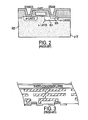
- other photosensitive elements for detecting and performing photoconversion of a light signal and subsequently or simultaneously amplifying the resulting electrical charge may be used instead, such as a photodiode or a stacked pixel sensor structure, wherein the effective light sensitive area may be significantly increased by the stacked structure.
- An example of a stacked pixel sensor structure is illustrated in FIG. 3 and described in fuller detail in " A Stacked CMOS APS For Charge Particle Detection And Its Noise Performance," by I. Takayanagi et al., IEEE Workshop on Charge-Coupled Devices and Advanced Image Sensors, pp. 159-162, June 1999 , the contents of which are hereby incorporated by reference.
- an imaging apparatus 800 includes an image sensor 802 having a pixel array arranged according to a Bayer color filter pattern.
- a charge multiplying photoconversion layer such as a HARP layer is provided over each of the pixels in the array under the filter pattern.
- Each pixel 804 contains the protection and readout circuits in accordance with any one of the various embodiments discussed herein above.
- the imaging apparatus 800 further includes a row decoder 806 includes a plurality of row select activation lines 808 corresponding in number to the number of rows in the pixel array of the image sensor 802, wherein each line is connected to each row select switch in all the pixels in a respective row of the array.
- column decoder 812 includes a plurality of column lines 812, the number of which corresponds to the number of columns in the pixel array of the image sensor 802. Each column line 812 is connected to the output sides of the row select switches in all the pixels in a respective column.
- controller 824 controls the row decoder 806 to sequentially activate the row select lines, whereby the row select switches for each pixel in a selected row is activated to thereby dump the image data from each respective pixel to the respective column line. Since each pixel in a row is connected to a different column line, the image data for each pixel is then read out to the image processor by sequentially activating all the column lines through column decoder 810. Thus, after activation of each row select line, the column lines are sequentially activated to collect the image data in an orderly manner across the array.
- the data Upon reading the image data out of the pixel array, the data is passed through a number of processing circuits which, in linear order, generally include a sample and hold circuit 814, an amplifier 816, an analog to digital converter 818, an image processor 820, and an output device 822.
- processing circuits which, in linear order, generally include a sample and hold circuit 814, an amplifier 816, an analog to digital converter 818, an image processor 820, and an output device 822.
- imaging apparatus 800 could be part of a computer system, camera system, scanner, machine vision system, vehicle navigation system, video telephone, surveillance system, auto focus system, star tracker system, motion detection system, image stabilization system and other systems requiring an imager.
- the imaging apparatus 800 may also be connected to a processor system 850, as shown in FIG. 15 , such as a computer system.
- a processor system 850 generally comprises a central processing unit (CPU) 852 that communicates with an input/output (I/O) device 854 over a bus 856.
- the imaging apparatus 800 communicates with the system over bus 856 or a ported connection.
- the processor system 800 also includes random access memory (RAM) 858, and, in the case of a computer system, may include peripheral devices such as a floppy disk drive 860 and a compact disc (CD) ROM drive 862 which also communicate with CPU 852 over the bus 856.
- RAM random access memory
Landscapes
- Engineering & Computer Science (AREA)
- Physics & Mathematics (AREA)
- Signal Processing (AREA)
- Multimedia (AREA)
- Power Engineering (AREA)
- Nonlinear Science (AREA)
- Electromagnetism (AREA)
- Condensed Matter Physics & Semiconductors (AREA)
- General Physics & Mathematics (AREA)
- Computer Hardware Design (AREA)
- Microelectronics & Electronic Packaging (AREA)
- Computer Vision & Pattern Recognition (AREA)
- Solid State Image Pick-Up Elements (AREA)
- Transforming Light Signals Into Electric Signals (AREA)
- Light Receiving Elements (AREA)
- Thin Film Transistor (AREA)
- Metal-Oxide And Bipolar Metal-Oxide Semiconductor Integrated Circuits (AREA)
- Bipolar Transistors (AREA)
Abstract
Description
- The present invention relates to image sensors which use a stacked avalanche multiplication layer to amplify the intensity of light captured by a pixel circuit.
- Amid the rising popularity for digital image devices such as digital cameras is a demand for increasingly higher picture resolution and for increasingly compact designs of such devices. Due to the interior space constraints in the housings of the compact designs, it is necessary to reduce the sizes of the electronic circuits in the device, including the image sensor. However, upon shrinking the size of the image sensor, a tradeoff must be made between resolution and the signal levels outputted from the image sensor. If the resolution is kept the same upon reducing the size of the image sensor, the size of each pixel must be proportionately reduced. Smaller pixels reduce the amount of charge that can be collected by each pixel during image exposure, which in turn reduces the sensitivity of the image sensor. Although the reduced sensitivity effect can be offset by increasing the integration (exposure) time, this is an undesirable "solution" because increasing integration time also increases the potential for obtaining a blurred image if there is any movement by the image subject or the device during exposure. On the other hand, in order to maintain the same sensitivity without having to increase integration time, the pixels must be made larger, which limits the resolution.
- One solution towards achieving both a more compact size and high image quality is disclosed in "CMOS Image Sensor Overlaid with a HARP Photoconversion Layer," by T. Watabe, et al., published in the Program of the 1999 IEEE Workshop on Charge-Coupled Devices and Advanced Image Sensors, pp. 211-214. In this image sensor, which is shown in
FIGS. 1A and 1B , thepixel circuit 902 is overlaid with a stacked charge multiplying photoconversion layer, such as a high-gain avalanche rushing amorphous photoconductor ("HARP") photo-conversion layer 904 for amplifying the light signal produced by each pixel. - When a photon 906 hits the
upper surface 908 of theHARP layer 904, acharge 910 in the form of holes is generated and amplified to many times its original level while being propelled through theHARP layer 904 to thebottom side 912. Thepixel circuit 902 is electrically connected to thebottom side 912 of theHARP layer 904 such that the amplifiedlight signal 910, upon reaching thebottom side 912 ofHARP layer 904, is conducted into thepixel circuit 902 as electrical charge. The charge accumulates at astorage node 914 in the pixel circuit until the pixel data is read out by activating the gate of arow select switch 916. The amount of charge accumulated at thenode 914, which is proportional to the intensity of light 906 detected, is read out. In this manner, the image sensor ofFIGS. 1A and 1B allows each pixel to capture image data with an intensity and sensitivity equivalent to that attainable by significantly larger pixels which do not have the avalanche multiplication capability. As a result, use of a HARP layer enables the image quality to be improved without having to increase the size of the image sensor array. - In order to obtain avalanche multiplication in the HARP layer, an electric field of about 106 V/cm is required, which is achieved by applying an operating voltage of between 50 -100 V to the HARP layer. In a typical HARP image sensor, voltages of less than about 8 V are used in the pixel circuit connected beneath the HARP layer, with the pixel circuit generally having a breakdown voltage of around 20 V. When the intensity of the incident light on the image sensor is at the upper end of the detection range for the charge multiplying photoconversion layer, the voltage level accumulating at the storage diode beneath the HARP layer approaches the level of the operating voltage applied to the HARP layer. Thus, voltages of 50-100 V may be applied to the storage diode when the image sensor is exposed to a strong light, resulting in a breakdown of the readout components of the pixel circuit.
- To address this problem, attempts have been made to build a pixel circuit having a higher breakdown tolerance. An example of such a high tolerance pixel circuit is disclosed in the article by T. Watabe et al. mentioned above, in which the pixel circuit is constructed as MOS transistor having a double drain structure. This structure is shown in
FIG. 2 , in which the n-doped drain formed in the p-dopedsilicon layer 922 includes a low-dose n- region 924 surrounding a conventional high-dose n+ region 926. The double drain MOS transistor structure was shown to achieve an endurance voltage up to just under 60 V. However, a special MOS fabrication process is required for forming the double drain MOS transistor, and the size of the MOS transistor makes it difficult to attain small pixel sizes for high resolution image sensors. - Another problem encountered in typical HARP image sensors when the voltage level at the storage node rises is that the effective voltage applied across the photoconversion layer decreases, which affects the charge amplification function of the photoconversion layer. For example, in the arrangement shown in
FIGS. 1A and 1B , as the charge representing a detected light flows from theHARP layer 904 and accumulates on thenode 914 of the storage diode, the voltage at thenode 914 increases, causing the potential difference between the operating voltage Vtarget applied to theHARP layer 904 and thestorage node 914 to decrease. The result is pixel signal saturation and a nonlinear response in which the signal levels recorded by the imaging device are not correctly represented in the pixel output. - To address this problem, it is necessary to find a way to amplify the intensity of light signals by the same amount under bright light conditions as for lower light conditions, by either accounting for the loss of effective operating voltage across the charge multiplying photoconversion layer or otherwise addressing the decreasing amplification in bright light conditions.
US 5818052 discloses a low light level solid state image sensor. The high sensitivity at low light level is achieved by an image sensor combination of a photoconductor with high avalanche detection gain, a silicon detector with very high gain pixel level amplifiers and noise suppression circuits. A high gain avalanche rushing photoconductor (HARP) sensor device is connected to an amplified metal oxide silicon (AMOS) device and a low noise readout device. The high sensitivity image sensor is fabricated by depositing an amorphous Selenium photoconductive layer on the top of a silicon junction diode or a Palladium Silicide, (Pd2Si) Schottky barrier diode that is connected to the AMOS pixel amplifier circuits to form a two story circuit.
In "CMOS image sensor overlaid with a HARP photoconversion film", published in Conference Proceedings on Optoelectronic and Microelectronic Materials and Devices, 6 December 2000, pages 89-92, Bandoora, Australia, Yamauchi et al disclosed new CMOS image sensor that was made by overlaying a HARP (high-gain avalanche rushing amorphous photoconductor) photo-conversion film on to the CMOS readout circuit. Prototype sensors were fabricated that used a new MOS transistor to increase breakdown voltage in the readout circuit. Connecting processes were developed and used to connect the HARP film to the readout circuit. Stable operation of the sensor was observed when the target voltage of 60 volts was applied.
US 5371392 discloses a semiconductor apparatus and horizontal register for solid state image pickup apparatus with a protection circuit. A semiconductor apparatus connected between a signal input line and a grounding line is formed on a semiconductor substrate with a protection circuit connected between the signal input line and the grounding line, in parallel with the semiconductor apparatus. The protection circuit is formed, for example, of bipolar transistors, diodes, or MOS transistors.
EP 1187217 discloses a solid state image-sensing device having a photosensitive element that produces an electric signal commensurate with the amount of light incident thereon, a transistor of which the first electrode and the control electrode are connected to one electrode of the photosensitive element, and a resetting portion for resetting the transistor by feeding a predetermined pulse signal to the second electrode of the transistor The resetting portion resets the transistor in such a way as to inhibit the transistor from operating in a subthreshold region when the amount of light incident on the photosensitive element is below a predetermined level. - A first aspect of the present invention serves to mitigate problems associated with the high voltages which may be generated by a HARP layer under bright light conditions by incorporating a protection circuit into the pixel circuit connected to the HARP layer. The protection circuits prevents the pixel circuit from breaking down when the voltage in the pixel circuit reaches the operating voltage applied to the charge multiplying photoconversion layer in response to the image sensor being exposed to a strong light, by limiting a voltage which accumulates at the charge storage element to a reference potential. In particular, the protection circuit of the present invention may be designed in any of several configurations is which additional voltage entering the pixel circuit from the charge multiplying photoconversion layer over a predetermined threshold voltage level is dissipated before reaching the storage node and other lower voltage components downstream therefrom.
- A second aspect of the present invention addresses the problem of pixel saturation and nonlinear amplification of the image signal output from a charge multiplying photoconversion layer by incorporating an output control circuit into the pixel circuit connected to the charge multiplying photoconversion layer. Preferably, the output control circuit is constructed as a charge trans-impedance amplifier (CTIA) circuit including at least an operational amplifier, wherein the CTIA serves to fix the voltage level at the storage node two thereby maintain a constant effective operating potential across the charge multiplying photoconversion layer.
- In one exemplary embodiment of the output control circuit in accordance with the invention, the effective voltage is maintained across a photo-conversion element at a , constant level to provide a linear output throughout the entire operating range of the photoconversion element. Another exemplary embodiment of an output control circuit in accordance with the invention also fixes the voltage across the photoconversion element, and further logarithmically compresses the image signal obtained from the photoconversion element. A third exemplary embodiment of the output control circuit provides a linear output signal in low light conditions until the current from the photoconversion element reaches a predetermined threshold value, whereupon the output control circuit then switches the output to a logarithmic signal in brighter light conditions. Optionally, the output control circuit of this last embodiment may be constructed so that the threshold value between the linear and logarithmic output characteristics is adjustable.
- These and other features and advantages of embodiments of the present invention will become more apparent from the following detailed description which is provided with reference to the accompanying drawings.
-
FIG. 1A is a cross-sectional view of a pixel in an image sensor having a charge multiplying photoconversion layer as known in the art; -
FIG. 1B is a circuit diagram of the pixel arrangement shown inFIG. 1A ; -
FIG. 2 is a cross-sectional view of a double-drain MOS transistor as known in the art; -
FIG. 3 is an illustration of an alternative photoconversion element usable with the present invention; -
FIG. 4 is a circuit diagram of a first preferred embodiment in accordance with the present invention; -
FIG. 5 is a circuit diagram of a second preferred embodiment in accordance with the present invention; -
FIG. 6 is a circuit diagram of a third preferred embodiment in accordance with the present invention; -
FIG. 7 is a circuit diagram of a fourth preferred embodiment in accordance with the present invention; -
FIG. 8 is a circuit diagram of a fifth embodiment in accordance with the present invention; -
FIG. 9 is a circuit diagram of a sixth embodiment in accordance with the present invention; -
FIG. 10 is a circuit diagram of a seventh embodiment in accordance with the present invention; -
FIG. 11 is a graph for illustrating the conversion characteristics obtained by the embodiment shown inFIG. 10 ; -
FIG. 12 is a circuit diagram of a eighth embodiment in accordance.with the present invention; -
FIG. 13 is a circuit diagram in accordance with a ninth embodiment of the present invention; -
FIG. 14 is an example of an imaging apparatus incorporating the present invention; and -
FIG. 15 is an illustration of a processing system communicating with the imaging apparatus of the present invention. - A first aspect of the present invention protects a pixel circuit connected to the HARP layer from breakdown caused by a high voltage transferred to the pixel circuit from the HARP layer under bright light conditions. The pixel circuit is protected from breakdown by incorporating therein a protection circuit which prevents excess voltage above a predetermined threshold level from reaching the components of the pixel circuit downstream from the protection circuit. A pixel structure in accordance with this aspect of the invention is described below with reference to
FIGS. 4-7 showing four exemplary embodiments of a protection circuit providing the capability described above. - A first exemplary embodiment of the invention is shown in
FIG. 4 , and is similar to the pixel arrangement shown inFIG. 1B in that it includes a charge (hole) multiplyingphotoconversion layer 102 connected to a voltage Vtarget at its upper plate and connected tostorage node 104 of astorage element 510 at its bottom plate. In this embodiment,storage element 510 is provided as astorage diode 106. Although the charge multiplying photoconversion layer is preferably a high-gain avalanche rushing amorphous photoconductor (HARP) photoconversion layer, other structures for detecting and performing photoconversion of a light signal and subsequently or simultaneously amplifying the resulting electrical charge may be used.Storage node 104 is the cathode ofstorage diode 106 for accumulating charge corresponding to image data being collected during the image sensor integration time. Anoutput circuit 500 is connected to and positioned downstream fromnode 104, for reading out the charge accumulated atstorage diode 106. As shown inFIG. 4 ,output circuit 500 may be simply constructed as a rowselect transistor 108. - The anode of
storage diode 106 is connected to ground so as to block current flow throughdiode 106 when the voltage atnode 104 is a higher level than the ground connection, which will always be the case when an image signal is received from the charge multiplyingphotoconversion layer 102, since the signal charges are holes. Thus, with respect tostorage diode 106, therefore, as long as the rowselect transistor 108 is open, charge flowing from charge multiplyingphotoconversion layer 102 as a result of the detection of light will accumulate atnode 104. - Row
select transistor 108 ofoutput circuit 500 is connected to acolumn readout line 110 so that when the gate for the rowselect transistor 108 is closed, the charge atstorage node 104 is transferred to thecolumn readout line 110. When the column line containing the relevant pixel is activated, the image data from the pixel is transferred out of thepixel circuit 100 into an image processor where that charge is translated into image data along with the data read out from the other pixels in the image sensor array, to thereby construct the output image. - In order to prevent the charge accumulating at
node 104 from reaching the breakdown point ofstorage diode 106 or rowselect transistor 108, aprotection circuit 520 comprising a protection diode 112, the anode of which is connected tonode 104 ofstorage diode 106. The cathode of protection diode 112 is connected to a voltage Vdd, so that when the voltage level atstorage node 104 reaches the level of Vdd, any additional voltage arriving from the charge multiplyingphotoconversion layer 102 is bled off away fromnode 104 toward the voltage source Vdd. In this manner, protection diode 112 serves to limit the voltage atnode 104 to Vdd. - Once voltage is bled off from
node 104 through protection diode 112, image data representing light intensities detected at the upper end of the capability range of charge multiplyingphotoconversion layer 102 will be lost. Thus, the voltage level at source Vdd should be set to strike a balance between minimizing the potential to lose image data acquired in the upper end of the detection range oflayer 102, and limiting the voltage atnode 104 to a comfortable level to avoid the risk of breakdown of thestorage diode 106 and the rowselect transistor 108. - A second exemplary embodiment of the invention is shown in
FIG. 5 , and is identical to the pixel circuit of the first embodiment except that thestorage element 510 is embodied as astorage capacitor 202 instead of a storage diode. Preferably,storage capacitor 202 has a large capacitance value per unit area, even more preferably in the rage of 2-5 fF/µ2c. Such a capacitor provides a higher capacitance value while reducing the space required for the charge storage region, relative to the use of a storage diode. - In this embodiment, charge from the charge multiplying
photoconversion layer 204 is stored in thecapacitor 202, until the voltage at thecapacitor 206 reaches Vdd. Additional voltage flowing tonode 206 from the charge multiplyingphotoconversion layer 204 is then directed through the protection diode 208 ofprotection circuit 520 so that the charge stored in thecapacitor 202 maintains a voltage of around Vdd. - A third exemplary embodiment of the invention, as shown in
FIG. 6 , is identical to the pixel circuit of the first embodiment, except that the protection diode of theprotection circuit 520 is replaced with an n-MOS transistor 302. Both the drain and the gate of thetransistor 302 are connected to thestorage diode 308 ofstorage element 510, and the source of thetransistor 302 is connected to a voltage potential of Vdd. - As in the embodiments described previously, charge from the image signal accumulates at the
storage node 304 until the voltage atnode 304 reaches and surpasses Vdd. Once this occurs, the higher voltage at the transistor drain causes the excess voltage to flow through the transistor, so that the voltage at thestorage node 304 remains around Vdd. - In a variant of this embodiment, the
storage diode 308 ofstorage element 510 may be replaced with the high capacity capacitor as described above with reference to the embodiment ofFIG. 5 . -
FIG. 7 shows a fourth exemplary embodiment of the invention, which is identical to the embodiment ofFIG. 4 except that theprotection circuit 520 further includes aresistor 402 positioned between thebottom plate 406 of the charge multiplyingphotoconversion layer 404 and thestorage diode 408 ofstorage element 510. The resistor preferably has a high resistance value which reduces the voltage passing through thepixel circuit 400 from the charge multiplyingphotoconversion layer 404 and thestorage diode 408 atnode 410. - The presence of
protection circuit 510, embodied here asprotection diode 412, provides additional protection for thepixel circuit 400, so that in the event the signal voltage flowing from the charge multiplyingphotoconversion layer 404 is significantly larger than Vdd that the voltage atnode 410 upon passing throughresistor 402 is still too high, the excess voltage will be directed away from thestorage diode 408 and the row select transistor 414 through theprotection diode 412. - A first variation of the
FIG. 7 embodiment may be provided by replacing thestorage diode 408 ofstorage clement 510 with the capacitor discussed above in the embodiment ofFIG 4 . Similarly, the present invention also encompasses a second variation of this embodiment in which theprotection diode 412 is replaced with an n-MOS transistor as described above in the embodiment ofFIG 5 . In a third variation of theFIG. 7 embodiment, both thestorage diode 408 ofstorage element 510 and theprotection diode 412 are replaced with the capacitor ofFIG. 5 and the n-MOS transistor ofFIG. 6 , respectively. - In an image sensor using a charge multiplying photoconversion layer, as the voltage level at the storage node rises, the effective voltage applied to the photoconversion layer decreases, which affects the charge amplification function of the photoconversion layer. For example, if the voltage Vtarget applied to the charge multiplying photoconversion layer is reduced, the amplification achieved by the photoconversion layer is also reduced. Thus, when the signal level is read out upon activating the row select switch, the signal level recorded by the imaging device will be less than the signal level actually detected.
- A second aspect of the present invention addresses this concern by incorporating into each pixel circuit an output control circuit which prevents the effective voltage across the photoconversion layer from decreasing during integration of light in the pixel. More specifically, the output control circuits according to this aspect of the invention serve to fix the voltage level at the storage node to maintain a constant effective operating potential across the charge multiplying photoconversion layer. The pixel structure disclosed herein will be further described below with reference to
FIGS. 8-13 showing five exemplary embodiments of the output circuit in accordance with this aspect of the invention. - According to a fifth embodiment of the invention, shown in
FIG. 8 , the pixel structure includes a charge multiplyingphotoconversion layer 502 connected to a voltage Vtarget at its upper plate. The bottom plate of the charge multiplyingphotoconversion layer 502 is connected tooutput circuit 500 which includes asignal generation circuit 600 and a rowselect switch 130.Signal generation circuit 600 controls the characteristics of the charge received from the charge multiplyingphotoconversion layer 502. Rowselect switch 130 is connected to the output side of thesignal generation circuit 600 for reading out the accumulated charge representing the image signal acquired from the charge multiplyingphotoconversion layer 502. Preferably, rowselect switch 130 is formed as a MOS transistor and operated by a gate signal transmitted by a controller, such as thecontroller 824 shown inFIG. 14 . - Row
select switch 130 is connected tocolumn readout line 110 so that when theswitch 130 is closed (for example, upon receiving a gate signal from a controller when the row select switch is a transistor), the output voltage of thesignal generation circuit 600 is transferred to acolumn readout line 110 and from there to a sample and hold circuit (see, e.g.,element 814 inFIG. 14 ). The image data from the pixel is transferred from the sample and hold circuit to a digitizer and then to an image processor where that charge is translated into image data along with the data read out from the other pixels in the image sensor array, to thereby construct the output image. - As seen in
FIG. 8 , thesignal generation circuit 600 according to this embodiment is a charge trans-impedance amplifier (CTIA) circuit which includes adifferential amplifier 128 connected to a constant voltage supply VREF at apositive input 114 thereof. VREF is set to a value slightly below the operating voltage of the differential amplifier to obtain sufficient output voltage swing. Afeedback loop 120 is formed between anoutput node 116 of thedifferential amplifier 128 and anegative input node 122 thereof, and acapacitor 118 is connected in thefeedback loop 120. Areset switch 126 is connected in asecond loop 124 formed between thenegative input node 122 and theoutput node 116 of thedifferential amplifier 128 and parallel to thefeedback loop 120, for shorting out thecapacitor 118 at the initialization period preceding each integration time. Rowselect switch 130 is also connected to theoutput node 116 of thedifferential amplifier 128 downstream of thefeedback loop 120 andsecond loop 124. - The
differential amplifier 128 forces the voltage at thenegative input node 122 to become fixed at VREF, which in turn maintains the effective operating potential Vtarget across the charge multiplyingphotoconversion layer 502 at a constant level, i.e., Vtarget- VREF. Since the multiplication factor to which an image signal is amplified in thephotoconversion layer 502 is a function of the applied bias to the photoconversion layer, fixing the potential at the at the output side of thephotoconversion layer 502, which is at the same potential as thenegative input node 122 to thedifferential amplifier 128, yields a constant multiplication factor of the image signals detected by the charge multiplyingphotoconversion layer 502. - During integration time in this pixel circuit, current from the
photoconversion layer 502 is integrated on thecapacitor 118. When the rowselect switch 130 is closed, the output voltage of thedifferential amplifier 128 is transferred to thecolumn readout line 110. Configured in this manner, the output voltage from thedifferential amplifier 128 represents the intensity of the detected incident light on thephotoconversion layer 502, and is given by Eq. 1 below: -

- wherein IHARP and tINT represent the current from the charge multiplying
photoconversion layer 502 and the integration time, respectively, and Cfb represents the capacitance of thecapacitor 118. - With the CTIA as shown in
FIG. 8 , thesignal generation circuit 600 provides a linear output along the entire operating range of charge multiplyingphotoconversion layer 502. -
FIG. 9 shows a pixel circuit in accordance with a second embodiment of the present invention. The pixel circuit of the sixth embodiment is generally the same as the pixel circuit discussed above with reference toFIG. 8 , except that thesignal generation circuit 600 inFIG. 8 is replaced bysignal generation circuit 610 in the embodiment shown inFIG. 9 . Components of this embodiment which are equivalent to those shown inFIG. 8 are identified inFIG. 9 with the same reference numerals, and description of those elements will be omitted in the description below. - Like
signal generation circuit 600,signal generation circuit 610 also fixes the potential at the output side of a charge multiplyingphotoconversion layer 502 and thenegative input node 122 to adifferential amplifier 128, so as to maintain a constant effective input node voltage across the charge multiplyingphotoconversion layer 502 to be Vtarget- VREF. Instead of a capacitor connected in the feedback loop, the CTIA circuit ofsignal generation circuit 610 includes afeedback diode 218 connected in afeedback loop 220 between theoutput node 116 and thenegative input node 122 of thedifferential amplifier 128. The anode of thefeedback diode 218 is connected to thenegative input node 122 of thedifferential amplifier 128 while the cathode of thefeedback diode 218 is connected to theoutput node 116 of the differential amplifier. The current flowing across thefeedback diode 218 is determined according to Eq. 2 below: -

- wherein I0 is the saturation current of the
feedback diode 218, q represents the charge of an electron (= 1.6 · 10-19 coulombs (C)), k is Boltzmann's constant (= 1.38 · 10-23 J/°K), T represents the temperature of the diode measured in degrees Kelvin, Vout is the output voltage from thedifferential amplifier 128, and IHARP represents the current from the charge multiplyingphotoconversion layer 502. - Using Eq. 2, the output voltage from the
differential amplifier 128 can be determined as set forth in Eq. 3: -

- As can be seen from Eq. 3, the presence of
feedback diode 218 in the feedback loop of thesignal generation circuit 610 operates to logarithmically compress the current IHARP flowing from the charge multiplyingphotoconversion layer 502 through thedifferential amplifier 128. Although the image signal obtained from the pixel circuit shown inFIGS. 1A and 1B becomes compressed due to the decreasing effective voltage across the photoconversion layer as the detected light level increases, logarithmically compressing the image signal with the CTIA of thesignal generation circuit 610 enables the pixel readout signal to be correlated much more predictably with the intensity of light actually detected at the photoconversion layer. - A seventh embodiment of the present invention is shown in
FIG. 10 and includes ansignal generation circuit 620 in place of the output control circuits 10 and 20 in the fifth and sixth embodiments described above. Components shown inFIG. 10 that are equivalent to the components shown inFIGS. 8 and 9 are identified with the same reference numerals, and discussion of those components will be omitted in the description of this embodiment below.Signal generation circuit 620 is constructed as a CTIA which includes afirst feedback loop 120 and asecond feedback loop 320 both connected between theoutput node 116 and thenegative input node 122 of adifferential amplifier 128. -
Feedback loop 120 includes acapacitor 118 for providing a linear output from thedifferential amplifier 128, similarly to the embodiment ofFIG. 8 .Feedback loop 320 is arranged in parallel tofeedback loop 120 and includes afeedback diode 218 and an offsetvoltage source 328 that applies a voltage Voff to the cathode offeedback diode 218. Offsetvoltage source 328 is connected to theoutput node 116 of adifferential amplifier 128 and to the cathode offeedback diode 218, while the anode of feedback diode is connected to thenegative input node 122 of thedifferential amplifier 128. Athird loop 124 contains areset switch 126 and is also connected between theoutput node 116 and thenegative input node 122 ofdifferential amplifier 128, in parallel tofeedback loops - The current IHARP from the
photoconversion layer 502 flows through the CTIA ofsignal generation circuit 620 according to Eq. 4 as follows: -

- The first term represents the current flowing across the
feedback diode 218 and the second term represents the current flowing to thefeedback capacitor 118. When VREF - Vout - Voff < 0, that is, when VREF - Voff < Vout < VREF, the second term of Eq. 4 is dominant. In this situation, no current flows through thefeedback diode 218, and the output voltage Vout from thesignal generation circuit 620 is determined according to Eq. 1 set forth above. - On the other hand, when VREF - Vout - Voff > 0, that is, when Vout < VREF - Voff, current flows through the
feedback diode 218 and becomes logarithmically compressed, as indicated by the first term in Eq. 4. When IHARP is sufficiently large, the second term becomes negligible, which yields an output voltage of thedifferential amplifier 128 according to Eq. 5 below: -

- The resulting conversion characteristics represented by Vout over time is shown in
FIG. 11 , where it can be clearly seen that linear conversion characteristics are obtained when Vout > VREF - Voff, and logarithmic conversion characteristics are obtained when Vout < VREF - Voff. Thus, the readout signal obtained from the pixel circuit shown inFIG. 10 varies linearly with the signal outputted from the charge multiplyingphotoconversion layer 502 in low light conditions, and varies logarithmically with the signal outputted from the charge multiplyingphotoconversion layer 502 in bright light conditions. - Optionally, the transition point at which the
signal generation circuit 620 switches from the linear conversion mode to the logarithmic conversion mode can be made to be adjustable by enabling a user to apply a variable reverse bias potential to thefeedback diode 218. This variation of the pixel circuit ofFIG. 10 is illustrated inFIG. 12 and discussed below as the eighth embodiment of the present invention. - The pixel circuit shown in
FIG. 12 is nearly identical to that shown inFIG. 10 , except that the offsetvoltage source 328 inFIG. 10 is replaced with an offsetcapacitor 430. Again, components inFIG. 12 that are equivalent to those shown in the previous drawings are identified with the same reference numerals, and descriptions of those elements will be omitted in the explanation of this embodiment provided below. - One terminal of a
switch 432 is connected to the offsetcapacitor 430 at anode 434 located along afeedback loop 320 between thecapacitor 430 and afeedback diode 218. The other terminal of theswitch 432 is connected to avoltage source 436 having a voltage VREF + Voff. The voltage level of Voff may be adjustable by a user to thereby adjust the transition point between the linear and logarithmic operation modes of the pixel circuit. The adjustable voltage Voff is applied to thefeedback diode 218 by closing theswitch 432 which enables current from thevoltage source 436 at the selected voltage level to flow to thecapacitor 430. Even if the level of Voff is not adjusted, the voltage level applied to the cathode offeedback diode 218 can be adjusted by controlling the length of time that theswitch 432 is closed, which controls the amount of charge in, and hence the voltage across thefeedback capacitor 430. - During the initialization period before the start of each integration time and before charging the offset
capacitor 430, theswitch 432 is closed along withreset switch 126 by a reset signal ΦRS. When theswitches capacitor 118 is shorted out to clear out any residual charge on the capacitors associated with the image signal most recently read out from the pixel circuit and thecapacitor 430 is charged to Voff. - A ninth embodiment of the present invention is shown in
FIG. 13 , and is identical to the embodiment shown inFIG. 12 , except that the embodiment shown inFIG. 13 further includes a circuit for performing a freeze frame shutter operation. Specifically, afreeze frame switch 542 and ahold capacitor 540 are connected in the pixel circuit between theoutput node 116 from thedifferential amplifier 128 and the rowselect switch 130.Freeze frame switch 542 is controlled by a transfer signal ΦT that closes thefreeze frame switch 542 to enable the image signal to flow to and be stored in thehold capacitor 540. When the freeze frame switch is opened, no further charge can accumulate in thehold capacitor 540. - After charging the
hold capacitor 540 with the image signal, the charge is held in the hold capacitor to enable the image signal for that pixel to be read out by closing the rowselect switch 130 for each readout operation. For example, when an image is captured by an entire image sensor pixel array, the image sensor can be operated in freeze frame mode in which the image signal for each pixel is frozen so that the image data from all the pixels in the array can be read out row by row. Thus, thefreeze frame switch 542 is closed and then opened by operation of the transfer signal ΦT to all of the pixels in the image sensor array at the same time, whereupon the row select signal is applied to the image sensor array row by row to read out the pixel image signals. - In the embodiments shown in
FIGS. 9 ,10 ,12 and 13 described above,feedback diode 218 may be implemented by use of the sub-threshold characteristics of a MOS transistor. It is readily understood by one of ordinary skill in the art that a MOS transistor has four operational modes depending on bias conditions: 1) when no bias is applied to the gate, the transistor is off and no current flows from the drain; 2) the transistor is in a subthreshold region when the gate voltage VG is less than a predetermined threshold voltage VT, wherein the current flowing from the drain is ID = I0 · exp{q(VG - VT)/kT}; 3) the transistor is in a saturation region when VG - VT < VD (drain voltage), wherein the current flowing from the drain is ID = (β/2) · (VG - VT)2; and 4) the transistor is in a linear region when VG - VT > VD, wherein the current flowing from the drain is
- In each of the fifth through ninth embodiments of the invention as shown in
FIGS. 8-13 , there is no storage element connected between the bottom plate of the charge multiplying photoconversion layer and the output control circuit as is the case in the first through fourth embodiments of the invention as shown inFIGS. 4-7 . Thus, in the embodiments ofFIGS. 8-13 , the bottom plate of the charge multiplying photoconversion layer is connected directly to theinput node 122 of the respectiveoutput control circuit 500. - An additional aspect of the invention provides a pixel structure having both an
output circuit 500 for maintaining a constant voltage across the charge multiplying photoconversion layer and aprotection circuit 520 for dissipating excess voltage over a predetermined threshold being outputted from the charge multiplying photoconversion layer into theoutput control circuit 500. Here, the bottom plate of the charge multiplying photoconversion layer is connected to both the negative input of thedifferential amplifier 128 in theoutput circuit 500 and the input to theprotection circuit 520. - A tenth embodiment of a pixel structure in accordance with this aspect of the invention is nearly identical to the fifth embodiment pixel structure shown in
FIG. 8 , but further includes a protection circuit connected to thenode 122 in theoutput control circuit 500. As with the protection circuits described above, the protection circuit in the tenth embodiment may be constructed as a diode such as the protection diode 112 shown and described above with reference toFIG. 4 , an n-MOS transistor such as the n-MOS transistor 302 shown and described above with reference toFIG. 6 , a resistor and a diode such as theresistor 402 andprotection diode 412 shown and described above with reference toFIG. 7 , or a resistor and an n-MOS transistor as disclosed above. - An eleventh embodiment of a pixel structure in accordance with this aspect of the invention is nearly identical to the sixth embodiment pixel structure shown in
FIG. 9 , and further includes a protection circuit connected to thenode 122 in theoutput control circuit 500. As with the protection circuits described above, the protection circuit in the eleventh embodiment may be constructed as a diode such as the protection diode 112 shown and described above with reference toFIG. 4 , an n-MOS transistor such as the n-MOS transistor 302 shown and described above with reference toFIG. 6 , a resistor and a diode such as theresistor 402 andprotection diode 412 shown and described above with reference toFIG. 7 , or a resistor and an n-MOS transistor as disclosed above. - A twelfth embodiment of a pixel structure in accordance with this aspect of the invention is nearly identical to the seventh embodiment pixel structure shown in
FIG. 10 , and further includes a protection circuit connected to thenode 122 in theoutput control circuit 500. As with the protection circuits described above, the protection circuit in the twelfth embodiment may be constructed as a diode such as the protection diode 112 shown and described above with reference toFIG. 4 , an n-MOS transistor such as the n-MOS transistor 302 shown and described above with reference toFIG. 6 , a resistor and a diode such as theresistor 402 andprotection diode 412 shown and described above with reference toFIG. 7 , or a resistor and an n-MOS transistor as disclosed above. - A thirteenth embodiment of a pixel structure in accordance with this aspect of the invention is nearly identical to the eighth embodiment pixel structure shown in
FIG. 12 , and further includes a protection circuit connected to the negative input to the differential amplifier in theoutput control circuit 500. As with the protection circuits described above, the protection circuit in the thirteenth embodiment may be constructed as a diode such as the protection diode 112 shown and described above with reference toFIG. 4 , an n-MOS transistor such as the n-MOS transistor 302 shown and described above with reference toFIG. 6 , a resistor and a diode such as theresistor 402 andprotection diode 412 shown and described above with reference toFIG. 7 , or a resistor and an n-MOS transistor as disclosed above. - A fourteenth embodiment of a pixel structure in accordance with this aspect of the invention is nearly identical to the ninth embodiment pixel structure shown in
FIG. 13 , and further includes a protection circuit connected to the negative input to thedifferential amplifier 128 in theoutput control circuit 500. As with the protection circuits described above, the protection circuit in the fourteenth embodiment may be constructed as a diode such as the protection diode 112 shown and described above with reference toFIG. 4 , an n-MOS transistor such as the n-MOS transistor 302 shown and described above with reference toFIG. 6 , a resistor and a diode such as theresistor 402 andprotection diode 412 shown and described above with reference toFIG. 7 , or a resistor and an n-MOS transistor as disclosed above. circuit does not affect the operation of the pixel since the input to the differential amplifier is fixed at VREF. However, if a storage element is present and if the differential amplifier and the feedback loop(s) are malfunctioning, the current may then accumulate at the storage element. - In each of the embodiments described above, the charge multiplying photoconversion layer is preferably a high-gain avalanche rushing amorphous photo conductor (HARP) photoconversion layer. Alternatively, however, other photosensitive elements for detecting and performing photoconversion of a light signal and subsequently or simultaneously amplifying the resulting electrical charge may be used instead, such as a photodiode or a stacked pixel sensor structure, wherein the effective light sensitive area may be significantly increased by the stacked structure. An example of a stacked pixel sensor structure is illustrated in
FIG. 3 and described in fuller detail in "A Stacked CMOS APS For Charge Particle Detection And Its Noise Performance," by I. Takayanagi et al., IEEE Workshop on Charge-Coupled Devices and Advanced Image Sensors, pp. 159-162, June 1999, the contents of which are hereby incorporated by reference. - An example of an imaging device incorporating the present invention is shown in
FIG. 14 . Specifically, animaging apparatus 800 includes animage sensor 802 having a pixel array arranged according to a Bayer color filter pattern. A charge multiplying photoconversion layer such as a HARP layer is provided over each of the pixels in the array under the filter pattern. Eachpixel 804 contains the protection and readout circuits in accordance with any one of the various embodiments discussed herein above. - The
imaging apparatus 800 further includes arow decoder 806 includes a plurality of rowselect activation lines 808 corresponding in number to the number of rows in the pixel array of theimage sensor 802, wherein each line is connected to each row select switch in all the pixels in a respective row of the array. Similarly, column decoder 812 includes a plurality of column lines 812, the number of which corresponds to the number of columns in the pixel array of theimage sensor 802. Each column line 812 is connected to the output sides of the row select switches in all the pixels in a respective column. - To read the image data obtained by the
image sensor 802,controller 824 controls therow decoder 806 to sequentially activate the row select lines, whereby the row select switches for each pixel in a selected row is activated to thereby dump the image data from each respective pixel to the respective column line. Since each pixel in a row is connected to a different column line, the image data for each pixel is then read out to the image processor by sequentially activating all the column lines throughcolumn decoder 810. Thus, after activation of each row select line, the column lines are sequentially activated to collect the image data in an orderly manner across the array. - Upon reading the image data out of the pixel array, the data is passed through a number of processing circuits which, in linear order, generally include a sample and hold
circuit 814, anamplifier 816, an analog todigital converter 818, animage processor 820, and anoutput device 822. - Without being limiting, such the
imaging apparatus 800 could be part of a computer system, camera system, scanner, machine vision system, vehicle navigation system, video telephone, surveillance system, auto focus system, star tracker system, motion detection system, image stabilization system and other systems requiring an imager. - The
imaging apparatus 800 may also be connected to aprocessor system 850, as shown inFIG. 15 , such as a computer system. Aprocessor system 850 generally comprises a central processing unit (CPU) 852 that communicates with an input/output (I/O)device 854 over abus 856. Theimaging apparatus 800 communicates with the system overbus 856 or a ported connection. Theprocessor system 800 also includes random access memory (RAM) 858, and, in the case of a computer system, may include peripheral devices such as afloppy disk drive 860 and a compact disc (CD)ROM drive 862 which also communicate withCPU 852 over thebus 856. - Although the present invention has been described in relation to particular embodiments thereof, many other variations and modifications and other uses will become apparent to those skilled in the art. Therefore, the present invention is to be limited not by the specific disclosure herein, but only by the appended claims.
Claims (31)
- An image sensor pixel among an array of pixels in an image sensor, comprising:a charge multiplying photo-conversion element (102); anda charge storage element (510) electrically connected to the charge multiplying photoconversion element (102) at a first node (104), anda protection circuit (520) electrically characterised in that it is connected to the charge storage element (510) at the first node (104) and to a reference potential (Vdd) at a second node for limiting a voltage which accumulates at the charge storage element (510) to the reference potential.
- The image sensor pixel according to claim 1, wherein the charge multiplying photoconversion element (102) is a high gain avalanche rushing amorphous photoconductor photoconversion layer.
- The image sensor pixel according to claim 1, wherein the charge multiplying photoconversion element (102) is a stacked pixel structure.
- The image sensor pixel according to claim 1, wherein the storage element (510) is a junction photodiode (106), the cathode of which is connected to the charge multiplying photoconversion element.
- The image sensor pixel according to claim 1, wherein the storage element (510) is a capacitor (202).
- The image sensor pixel according to claim 1, wherein the protection circuit (520) includes a protection diode (112) electrically connected to the storage element (510) at the anode thereof and connected to the reference potential (Vdd) at the cathode thereof, whereby voltage accumulating at the storage element (510) in excess of the reference potential (Vdd) is transferred away from the storage element (510) through the protection diode (112).
- The image sensor pixel according to claim 6, wherein the protection circuit (520) further comprises a resistor (402) electrically connected between the charge multiplying photo-conversion element (102) and the storage element (510).
- The image sensor pixel according to claim 1, wherein the protection circuit (520) includes an n-MOS transistor (302) having a drain and a gate both electrically connected to the storage element (510), and a source electrically connected to the reference potential (Vdd), whereby voltage accumulating at the storage element (510) in excess of the reference potential (Vdd) is transferred away from the storage element (510) through the n-MOS transistor (302).
- The image sensor pixel according to claim 8, wherein the protection circuit (520) further comprises a resistor (420) electrically connected between the charge multiplying photo-conversion element (102) and the storage element (510).
- The image sensor pixel according to claim 1, further comprising an output circuit (500) connected to the charge storage element (510) and to the protection circuit (520).
- The image sensor pixel according to claim 10, wherein the output circuit (500) includes a row select transistor (108) which reads out the charge stored at the charge storage element (510).
- An image sensor comprising:a charge multiplying photoconversion element (502); andan image sensor pixel array having a plurality of pixels, wherein each pixel comprises:an output circuit (500) connected to the charge multiplying photoconversion element characterised in that the output control circuit is configured to maintain the potential across the charge multiplying photoconversion element at a predetermined voltage level.
- A method for obtaining an image signal, comprising:detecting a light signal in an image sensor;photoconverting the light signal into an electrical signal in a photosensitive element (102) in the image sensor;amplifying the electrical signal in the photosensitive element (102);transferring the electrical signal to a storage element (510) at a first node (104);accumulating charge from the electrical signal at the storage element (510); andlimiting the voltage at the storage element (510) to a reference potential (Vdd) using a protection circuit (520) connected to the photosensitive element (102) and the storage element (510) at the first node (104) and to the reference potential (Vdd) at a second node.
- The method according to claim 13, wherein limiting the voltage includes transferring charge away from the storage element (510) when the voltage resulting from the accumulated charge exceeds the reference potential.
- The method according to claim 14, wherein limiting the voltage further includes lowering the voltage of the electrical signal prior to the charge accumulating at the storage element (510).
- The method according to claim 13, further comprising reading out the charge accumulated at the storage element (510).
- A method for obtaining an image signal, comprising:detecting a light signal in an image sensor;photoconverting the light signal into an electrical signal with a charge multiplying photosensitive element (502) of the image sensor;amplifying the electrical signal in the charge multiplying photosensitive element (502); sandmaintaining the potential across the photosensitive element (502) to be constant at a predetermined voltage level.
- The method according to claim 17, further comprising performing a linear conversion of the electrical signal outputted from the photosensitive element (502) over the entire operating range of the photosensitive element (502).
- The method according to claim 17, further comprising logarithmically compressing the electrical signal outputted from the photosensitive element (502) over the entire operating range of the photosensitive element (502).
- The method according to claim 17, further comprising performing a linear conversion of the electrical signal outputted from the photosensitive element (502) when the outputted electrical signal is within a first range up to a predetermined threshold level, and logarithmically compressing the electrical signal when the outputted electrical signal is within a second range above the threshold level.
- The method according to claim 20, further comprising adjusting the threshold level at which the output control circuit switches from performing linear conversion of the electrical signal to logarithmic compression of the electrical signal.
- The method according to claim 17, further comprising performing a freeze frame operation on the electrical signal obtained by the charge multiplying photosensitive element (502).
- The method according to claim 17, wherein maintaining a constant potential across the photosensitive element (502) comprises limiting the voltage of the electrical signal outputted from the charge multiplying photosensitive element (502) to the predetermined voltage level.
- The method according to claim 23, wherein limiting the voltage includes transferring away a portion of the electrical signal which exceeds the predetermined voltage level.
- The method according to claim 24, wherein limiting the voltage further includes lowering the voltage of the electrical signal prior to transferring away the portion of the signal which exceeds the predetermined voltage level.
- An image processing apparatus comprising:an image sensor for detecting an image and outputting image signals corresponding to the detected image; andan image processor for processing the image signals outputted from the image sensor, wherein the image sensor includes the image sensor pixel of claim 1.
- A processing system, comprising:a processor for receiving and processing image data; andan image data generator for supplying image data to the processor, the image data generator comprisingan image sensor for detecting light and outputting an image signal,an image processor for processing the image signal, anda controller for controlling the image sensor and the image processor, wherein the image sensor includes the image sensor pixel of claim 1.
- An image processing apparatus comprising:the image sensor of claim 12 for detecting an image and outputting image signals corresponding to the detected image; andan image processor for processing the image signals outputted from the image sensor,wherein the charge multiplying photoconversion element has an input side for detecting a light signal and an output side for outputting the detected light signal as an electrical signal.
- The image processing apparatus of claim 28, wherein each pixel further comprises a protection circuit for limiting the voltage level at the output side of the charge multiplying photoconversion element at a predetermined voltage level.
- A processing system, comprising:a processor for receiving and processing image data; andan image data generator for supplying image data to the processor, the image data generator comprising:wherein the charge multiplying photo-conversion element has an input side for detecting a light signal and an output side for outputting the detected light signal as an electrical signal.the image sensor of claim 12 for obtaining an image and outputting an image signal,an image processor for processing the image signal, anda controller for controlling the image sensor and the image processor,
- The processing system of claim 30, wherein each pixel further comprises a protection circuit for limiting the voltage level at the output side of the charge multiplying photoconversion element at a predetermined voltage level.
Applications Claiming Priority (5)
| Application Number | Priority Date | Filing Date | Title |
|---|---|---|---|
| US226190 | 1988-08-02 | ||
| US226326 | 1999-01-06 | ||
| US10/226,190 US7372495B2 (en) | 2002-08-23 | 2002-08-23 | CMOS aps with stacked avalanche multiplication layer and low voltage readout electronics |
| US10/226,326 US6821808B2 (en) | 2002-08-23 | 2002-08-23 | CMOS APS with stacked avalanche multiplication layer which provides linear and logarithmic photo-conversion characteristics |
| PCT/US2003/026253 WO2004019609A2 (en) | 2002-08-23 | 2003-08-22 | A cmos aps with stacked avalanche multiplication layer and low voltage readout electronics |
Publications (2)
| Publication Number | Publication Date |
|---|---|
| EP1547152A2 EP1547152A2 (en) | 2005-06-29 |
| EP1547152B1 true EP1547152B1 (en) | 2009-04-08 |
Family
ID=31949786
Family Applications (1)
| Application Number | Title | Priority Date | Filing Date |
|---|---|---|---|
| EP03754405A Expired - Lifetime EP1547152B1 (en) | 2002-08-23 | 2003-08-22 | A cmos aps with stacked avalanche multiplication layer and low voltage readout electronics |
Country Status (9)
| Country | Link |
|---|---|
| US (5) | US7372495B2 (en) |
| EP (1) | EP1547152B1 (en) |
| JP (1) | JP2005536930A (en) |
| KR (1) | KR100681097B1 (en) |
| CN (2) | CN101309351A (en) |
| AT (1) | ATE428185T1 (en) |
| AU (1) | AU2003272232A1 (en) |
| DE (1) | DE60327087D1 (en) |
| WO (1) | WO2004019609A2 (en) |
Cited By (1)
| Publication number | Priority date | Publication date | Assignee | Title |
|---|---|---|---|---|
| EP4130657A4 (en) * | 2020-03-24 | 2023-09-06 | Sony Semiconductor Solutions Corporation | Light reception device and distance measurement device |
Families Citing this family (57)
| Publication number | Priority date | Publication date | Assignee | Title |
|---|---|---|---|---|
| US6791378B2 (en) * | 2002-08-19 | 2004-09-14 | Micron Technology, Inc. | Charge recycling amplifier for a high dynamic range CMOS imager |
| US7372495B2 (en) * | 2002-08-23 | 2008-05-13 | Micron Technology, Inc. | CMOS aps with stacked avalanche multiplication layer and low voltage readout electronics |
| US6780666B1 (en) * | 2003-08-07 | 2004-08-24 | Micron Technology, Inc. | Imager photo diode capacitor structure with reduced process variation sensitivity |
| JP2005183538A (en) * | 2003-12-17 | 2005-07-07 | Sumitomo Electric Ind Ltd | Light receiving element and optical receiver |
| US7383307B2 (en) * | 2004-01-07 | 2008-06-03 | International Business Machines Corporation | Instant messaging windowing for topic threads |
| JP4556722B2 (en) | 2004-05-31 | 2010-10-06 | コニカミノルタホールディングス株式会社 | Imaging device |
| JP2005348005A (en) * | 2004-06-02 | 2005-12-15 | Konica Minolta Holdings Inc | Imaging apparatus, imaging system, and imaging system operation program |
| US8035142B2 (en) * | 2004-07-08 | 2011-10-11 | Micron Technology, Inc. | Deuterated structures for image sensors and methods for forming the same |
| US7309878B1 (en) * | 2004-07-26 | 2007-12-18 | U.S. Department Of Energy | 3-D readout-electronics packaging for high-bandwidth massively paralleled imager |
| US7233051B2 (en) * | 2005-06-28 | 2007-06-19 | Intel Corporation | Germanium/silicon avalanche photodetector with separate absorption and multiplication regions |
| US7508434B2 (en) * | 2005-06-28 | 2009-03-24 | Motorola, Inc. | Image sensor architecture employing one or more floating gate devices |
| JP4212623B2 (en) * | 2006-01-31 | 2009-01-21 | 三洋電機株式会社 | Imaging device |
| US7652706B2 (en) * | 2006-02-15 | 2010-01-26 | Eastman Kodak Company | Pixel analog-to-digital converter using a ramped transfer gate clock |
| KR100789364B1 (en) | 2006-08-07 | 2007-12-28 | 연세대학교 산학협력단 | Optoelectronic mixer based on cmos |
| KR100879386B1 (en) * | 2006-11-13 | 2009-01-20 | 삼성전자주식회사 | Cmos image senser and digital camera including thereof and image signal detecting method of cmos image senser |
| US7923800B2 (en) * | 2006-12-27 | 2011-04-12 | Semiconductor Energy Laboratory Co., Ltd. | Semiconductor device and electronic device |
| US7547889B2 (en) * | 2007-03-16 | 2009-06-16 | Csem Centre Suisse D'electronique Et De Microtechnique Sa | Photon detection device |
| US7755685B2 (en) * | 2007-09-28 | 2010-07-13 | Sarnoff Corporation | Electron multiplication CMOS imager |
| FR2924862B1 (en) | 2007-12-10 | 2010-08-13 | Commissariat Energie Atomique | PHOTOSENSITIVE MICROELECTRONIC DEVICE WITH AVALANCHE MULTIPLIERS |
| WO2010079613A1 (en) * | 2009-01-09 | 2010-07-15 | パイオニア株式会社 | Imaging device |
| JP4835710B2 (en) * | 2009-03-17 | 2011-12-14 | ソニー株式会社 | Solid-state imaging device, method for manufacturing solid-state imaging device, driving method for solid-state imaging device, and electronic apparatus |
| EP2446613B1 (en) * | 2009-06-22 | 2019-07-24 | Trixell | Processing circuit for an x-ray sensor |
| KR101605831B1 (en) * | 2009-08-24 | 2016-03-24 | 삼성전자주식회사 | Cmos image senser and image signal detecting method thereof |
| JP2011071482A (en) | 2009-08-28 | 2011-04-07 | Fujifilm Corp | Solid-state imaging device, process of making the same, digital still camera, digital video camera, mobile phone, and endoscope |
| JP5409291B2 (en) * | 2009-11-19 | 2014-02-05 | 富士フイルム株式会社 | Solid-state imaging device, imaging device |
| US8817173B2 (en) * | 2010-02-01 | 2014-08-26 | Olympus Imaging Corp. | Photographing apparatus capable of flash emission |
| US8199238B2 (en) | 2010-04-30 | 2012-06-12 | Truesense Imaging, Inc. | Electronic shutter control in image sensors |
| US8184186B2 (en) * | 2010-04-30 | 2012-05-22 | Truesense Imaging, Inc. | Electronic shutter control in image sensors |
| US8203638B2 (en) * | 2010-04-30 | 2012-06-19 | Truesense Imaging, Inc. | Electronic shutter control in image sensors |
| US8184187B2 (en) * | 2010-04-30 | 2012-05-22 | Truesense Imaging, Inc. | Controlling electronic shutter in image sensors |
| JP5542091B2 (en) * | 2010-05-18 | 2014-07-09 | 富士フイルム株式会社 | Solid-state imaging device and imaging apparatus |
| DE102010027128A1 (en) * | 2010-07-14 | 2012-01-19 | Pnsensor Gmbh | Semiconductor component, in particular radiation detector, with an integrated overvoltage protection |
| US8390712B2 (en) | 2010-12-08 | 2013-03-05 | Aptina Imaging Corporation | Image sensing pixels with feedback loops for imaging systems |
| WO2013180690A1 (en) * | 2012-05-29 | 2013-12-05 | Hewlett-Packard Development Company, L.P. | Devices including independently controllable absorption region and multiplication region electric fields |
| US9219449B2 (en) * | 2012-07-24 | 2015-12-22 | Forza Silicon Corporation | CTIA for IR readout integrated circuits using single ended OPAMP with in-pixel voltage regulator |
| WO2014030551A1 (en) | 2012-08-23 | 2014-02-27 | ソニー株式会社 | Current/voltage conversion circuit and image pickup device |
| US9160949B2 (en) * | 2013-04-01 | 2015-10-13 | Omnivision Technologies, Inc. | Enhanced photon detection device with biased deep trench isolation |
| US11064142B1 (en) * | 2013-09-11 | 2021-07-13 | Varex Imaging Corporation | Imaging system with a digital conversion circuit for generating a digital correlated signal sample and related imaging method |
| CN103686006B (en) * | 2013-12-24 | 2017-04-05 | 北京交通大学 | A kind of global formula exposure cmos image sensor based on compression sensing |
| US9380229B2 (en) * | 2014-02-28 | 2016-06-28 | Samsung Electronics Co., Ltd. | Digital imaging systems including image sensors having logarithmic response ranges and methods of determining motion |
| WO2016145127A1 (en) * | 2015-03-09 | 2016-09-15 | California Institute Of Technology | Mid-infrared hyperspectral spectroscopy systems and methods thereof |
| JP6587123B2 (en) * | 2015-06-08 | 2019-10-09 | パナソニックIpマネジメント株式会社 | Imaging device |
| EP3411733A4 (en) * | 2016-02-01 | 2019-08-28 | Shenzhen Xpectvision Technology Co., Ltd. | X-ray detectors capable of managing charge sharing |
| US10811447B2 (en) * | 2016-03-04 | 2020-10-20 | Sony Corporation | Solid-state imaging device, driving method, and electronic equipment |
| CN107195645B (en) * | 2016-03-14 | 2023-10-03 | 松下知识产权经营株式会社 | Image pickup apparatus |
| KR102456297B1 (en) | 2016-04-15 | 2022-10-20 | 삼성디스플레이 주식회사 | Pixel circuit and method of driving the same |
| DE102016220492A1 (en) * | 2016-10-19 | 2018-04-19 | Fraunhofer-Gesellschaft zur Förderung der angewandten Forschung e.V. | Charge avalanche photodetector system |
| EP3367562A1 (en) * | 2017-02-22 | 2018-08-29 | Comet AG | High power amplifier circuit with protective feedback circuit |
| CN106950775A (en) * | 2017-05-16 | 2017-07-14 | 京东方科技集团股份有限公司 | A kind of array base palte and display device |
| US10574913B2 (en) * | 2017-09-07 | 2020-02-25 | Teledyne Scientific & Imaging, Llc | High dynamic range CTIA pixel |
| EP3848965A1 (en) * | 2018-09-06 | 2021-07-14 | Panasonic Intellectual Property Management Co., Ltd. | Solid-state imaging element, imaging system, method for driving solid-state imaging element, and photodetector |
| US10739807B2 (en) | 2018-09-11 | 2020-08-11 | Stmicroelectronics (Crolles 2) Sas | Body biasing for ultra-low voltage digital circuits |
| CN110160647B (en) * | 2019-06-20 | 2022-07-05 | 京东方科技集团股份有限公司 | Light intensity detection circuit, light intensity detection method and display device |
| US10892757B1 (en) | 2019-11-25 | 2021-01-12 | Stmicroelectronics (Research & Development) Limited | Reverse body biasing of a transistor using a photovoltaic source |
| CN111263089B (en) * | 2020-05-06 | 2020-10-16 | 深圳市汇顶科技股份有限公司 | Pixel, image sensor and electronic device |
| US11570391B2 (en) * | 2020-12-15 | 2023-01-31 | Sony Semiconductor Solutions Corporation | Digitally-calibrated CTIA image sensor pixel |
| CN116868345A (en) * | 2021-02-26 | 2023-10-10 | 索尼半导体解决方案公司 | Pixel substrate and light receiving device |
Family Cites Families (18)
| Publication number | Priority date | Publication date | Assignee | Title |
|---|---|---|---|---|
| US4973833A (en) * | 1988-09-28 | 1990-11-27 | Minolta Camera Kabushiki Kaisha | Image sensor including logarithmic converters |
| JPH03272180A (en) * | 1990-03-22 | 1991-12-03 | Toshiba Corp | Semiconductor integrated circuit |
| EP0542152B1 (en) * | 1991-11-08 | 1999-07-14 | Canon Kabushiki Kaisha | Laminated solid-state image sensing apparatus and method of manufacturing the same |
| JP3318774B2 (en) * | 1992-06-29 | 2002-08-26 | ソニー株式会社 | Semiconductor device and solid-state imaging device |
| US5619040A (en) * | 1994-03-29 | 1997-04-08 | Shapiro; Stephen L. | Data acquisition system |
| GB2289983B (en) | 1994-06-01 | 1996-10-16 | Simage Oy | Imaging devices,systems and methods |
| JP2576433B2 (en) * | 1994-12-14 | 1997-01-29 | 日本電気株式会社 | Protection circuit for semiconductor device |
| US5818052A (en) * | 1996-04-18 | 1998-10-06 | Loral Fairchild Corp. | Low light level solid state image sensor |
| US5892222A (en) * | 1996-04-18 | 1999-04-06 | Loral Fairchild Corporation | Broadband multicolor photon counter for low light detection and imaging |
| EP0923067B1 (en) * | 1997-03-12 | 2004-08-04 | Seiko Epson Corporation | Pixel circuit, display device and electronic equipment having current-driven light-emitting device |
| US6369853B1 (en) * | 1997-11-13 | 2002-04-09 | Foveon, Inc. | Intra-pixel frame storage element, array, and electronic shutter method suitable for electronic still camera applications |
| JP2001024209A (en) | 1999-07-07 | 2001-01-26 | Toshiba Corp | Radiation imaging device |
| JP2001135851A (en) * | 1999-11-05 | 2001-05-18 | Minolta Co Ltd | Photoelectric conversion element and solid-state imaging device |
| US6437339B2 (en) * | 2000-03-24 | 2002-08-20 | Hologic, Inc. | Flat panel x-ray imager with gain layer |
| US6492655B2 (en) * | 2000-04-05 | 2002-12-10 | Fuji Photo Film Co., Ltd. | Method and apparatus for reading image information |
| JP3493405B2 (en) | 2000-08-31 | 2004-02-03 | ミノルタ株式会社 | Solid-state imaging device |
| TW550944B (en) * | 2001-03-09 | 2003-09-01 | Honda Motor Co Ltd | Photosensitive circuit |
| US7372495B2 (en) * | 2002-08-23 | 2008-05-13 | Micron Technology, Inc. | CMOS aps with stacked avalanche multiplication layer and low voltage readout electronics |
-
2002
- 2002-08-23 US US10/226,190 patent/US7372495B2/en active Active
- 2002-08-23 US US10/226,326 patent/US6821808B2/en not_active Expired - Lifetime
-
2003
- 2003-08-22 CN CNA2008101094617A patent/CN101309351A/en active Pending
- 2003-08-22 JP JP2004529806A patent/JP2005536930A/en active Pending
- 2003-08-22 WO PCT/US2003/026253 patent/WO2004019609A2/en active Application Filing
- 2003-08-22 AU AU2003272232A patent/AU2003272232A1/en not_active Abandoned
- 2003-08-22 KR KR1020057003103A patent/KR100681097B1/en active IP Right Grant
- 2003-08-22 DE DE60327087T patent/DE60327087D1/en not_active Expired - Lifetime
- 2003-08-22 AT AT03754405T patent/ATE428185T1/en not_active IP Right Cessation
- 2003-08-22 CN CNB038246252A patent/CN100499145C/en not_active Expired - Fee Related
- 2003-08-22 EP EP03754405A patent/EP1547152B1/en not_active Expired - Lifetime
-
2006
- 2006-04-18 US US11/405,621 patent/US7365773B2/en not_active Expired - Lifetime
-
2008
- 2008-04-02 US US12/078,643 patent/US7525588B2/en not_active Expired - Lifetime
-
2009
- 2009-03-25 US US12/411,122 patent/US7880791B2/en not_active Expired - Fee Related
Cited By (1)
| Publication number | Priority date | Publication date | Assignee | Title |
|---|---|---|---|---|
| EP4130657A4 (en) * | 2020-03-24 | 2023-09-06 | Sony Semiconductor Solutions Corporation | Light reception device and distance measurement device |
Also Published As
| Publication number | Publication date |
|---|---|
| US20040036786A1 (en) | 2004-02-26 |
| AU2003272232A1 (en) | 2004-03-11 |
| DE60327087D1 (en) | 2009-05-20 |
| CN100499145C (en) | 2009-06-10 |
| US20080225133A1 (en) | 2008-09-18 |
| US7525588B2 (en) | 2009-04-28 |
| EP1547152A2 (en) | 2005-06-29 |
| US20040046101A1 (en) | 2004-03-11 |
| US20060187330A1 (en) | 2006-08-24 |
| AU2003272232A8 (en) | 2004-03-11 |
| CN101309351A (en) | 2008-11-19 |
| JP2005536930A (en) | 2005-12-02 |
| US20090200455A1 (en) | 2009-08-13 |
| KR100681097B1 (en) | 2007-02-08 |
| US6821808B2 (en) | 2004-11-23 |
| US7880791B2 (en) | 2011-02-01 |
| KR20050083654A (en) | 2005-08-26 |
| ATE428185T1 (en) | 2009-04-15 |
| WO2004019609A2 (en) | 2004-03-04 |
| US7372495B2 (en) | 2008-05-13 |
| WO2004019609A3 (en) | 2004-05-13 |
| US7365773B2 (en) | 2008-04-29 |
| CN1689164A (en) | 2005-10-26 |
Similar Documents
| Publication | Publication Date | Title |
|---|---|---|
| EP1547152B1 (en) | A cmos aps with stacked avalanche multiplication layer and low voltage readout electronics | |
| US6011251A (en) | Method for obtaining a high dynamic range read-out signal of a CMOS-based pixel structure and such CMOS-based pixel structure | |
| US7075049B2 (en) | Dual conversion gain imagers | |
| US7679666B2 (en) | Solid-state logarithmic image sensing device | |
| US6836291B1 (en) | Image pickup device with integral amplification | |
| US6188056B1 (en) | Solid state optical imaging pixel with resistive load | |
| US7746383B2 (en) | Photodiode CMOS imager with column-feedback soft-reset for imaging under ultra-low illumination and with high dynamic range | |
| US7659928B2 (en) | Apparatus and method for providing anti-eclipse operation for imaging sensors | |
| JP3965049B2 (en) | Imaging device | |
| US6734907B1 (en) | Solid-state image pickup device with integration and amplification | |
| EP0858212A1 (en) | Method for obtaining a high dynamic range read-out signal of a CMOS-based pixel structure and such CMOS-based pixel structure | |
| US5268576A (en) | Infrared focal plane array processor with integration and low pass filter per pixel | |
| CA2111707C (en) | High photosensitivity and high speed wide dynamic range ccd image sensor | |
| US6917029B2 (en) | Four-component pixel structure leading to improved image quality | |
| US7619671B2 (en) | Method, apparatus and system for charge injection suppression in active pixel sensors | |
| US6972399B2 (en) | Reset voltage generation circuit for CMOS imagers | |
| JP4345145B2 (en) | Solid-state imaging device | |
| US7936039B2 (en) | Backside illuminated CMOS image sensor with photo gate pixel | |
| EP0507541B1 (en) | Infrared focal plane array processor with integrator and low pass filter per pixel |
Legal Events
| Date | Code | Title | Description |
|---|---|---|---|
| PUAI | Public reference made under article 153(3) epc to a published international application that has entered the european phase |
Free format text: ORIGINAL CODE: 0009012 |
|
| 17P | Request for examination filed |
Effective date: 20050322 |
|
| AK | Designated contracting states |
Kind code of ref document: A2 Designated state(s): AT BE BG CH CY CZ DE DK EE ES FI FR GB GR HU IE IT LI LU MC NL PT RO SE SI SK TR |
|
| AX | Request for extension of the european patent |
Extension state: AL LT LV MK |
|
| DAX | Request for extension of the european patent (deleted) | ||
| 17Q | First examination report despatched |
Effective date: 20080128 |
|
| GRAP | Despatch of communication of intention to grant a patent |
Free format text: ORIGINAL CODE: EPIDOSNIGR1 |
|
| GRAS | Grant fee paid |
Free format text: ORIGINAL CODE: EPIDOSNIGR3 |
|
| GRAA | (expected) grant |
Free format text: ORIGINAL CODE: 0009210 |
|
| AK | Designated contracting states |
Kind code of ref document: B1 Designated state(s): AT BE BG CH CY CZ DE DK EE ES FI FR GB GR HU IE IT LI LU MC NL PT RO SE SI SK TR |
|
| REG | Reference to a national code |
Ref country code: GB Ref legal event code: FG4D |
|
| REG | Reference to a national code |
Ref country code: CH Ref legal event code: EP |
|
| RAP2 | Party data changed (patent owner data changed or rights of a patent transferred) |
Owner name: APTINA IMAGING CORPORATION |
|
| REG | Reference to a national code |
Ref country code: IE Ref legal event code: FG4D |
|
| REF | Corresponds to: |
Ref document number: 60327087 Country of ref document: DE Date of ref document: 20090520 Kind code of ref document: P |
|
| NLT2 | Nl: modifications (of names), taken from the european patent patent bulletin |
Owner name: APTINA IMAGING CORPORATION Effective date: 20090429 |
|
| PG25 | Lapsed in a contracting state [announced via postgrant information from national office to epo] |
Ref country code: SI Free format text: LAPSE BECAUSE OF FAILURE TO SUBMIT A TRANSLATION OF THE DESCRIPTION OR TO PAY THE FEE WITHIN THE PRESCRIBED TIME-LIMIT Effective date: 20090408 |
|
| NLV1 | Nl: lapsed or annulled due to failure to fulfill the requirements of art. 29p and 29m of the patents act | ||
| PG25 | Lapsed in a contracting state [announced via postgrant information from national office to epo] |
Ref country code: FI Free format text: LAPSE BECAUSE OF FAILURE TO SUBMIT A TRANSLATION OF THE DESCRIPTION OR TO PAY THE FEE WITHIN THE PRESCRIBED TIME-LIMIT Effective date: 20090408 Ref country code: PT Free format text: LAPSE BECAUSE OF FAILURE TO SUBMIT A TRANSLATION OF THE DESCRIPTION OR TO PAY THE FEE WITHIN THE PRESCRIBED TIME-LIMIT Effective date: 20090908 Ref country code: AT Free format text: LAPSE BECAUSE OF FAILURE TO SUBMIT A TRANSLATION OF THE DESCRIPTION OR TO PAY THE FEE WITHIN THE PRESCRIBED TIME-LIMIT Effective date: 20090408 Ref country code: ES Free format text: LAPSE BECAUSE OF FAILURE TO SUBMIT A TRANSLATION OF THE DESCRIPTION OR TO PAY THE FEE WITHIN THE PRESCRIBED TIME-LIMIT Effective date: 20090719 |
|
| PG25 | Lapsed in a contracting state [announced via postgrant information from national office to epo] |
Ref country code: SE Free format text: LAPSE BECAUSE OF FAILURE TO SUBMIT A TRANSLATION OF THE DESCRIPTION OR TO PAY THE FEE WITHIN THE PRESCRIBED TIME-LIMIT Effective date: 20090708 Ref country code: NL Free format text: LAPSE BECAUSE OF FAILURE TO SUBMIT A TRANSLATION OF THE DESCRIPTION OR TO PAY THE FEE WITHIN THE PRESCRIBED TIME-LIMIT Effective date: 20090408 |
|
| PG25 | Lapsed in a contracting state [announced via postgrant information from national office to epo] |
Ref country code: RO Free format text: LAPSE BECAUSE OF FAILURE TO SUBMIT A TRANSLATION OF THE DESCRIPTION OR TO PAY THE FEE WITHIN THE PRESCRIBED TIME-LIMIT Effective date: 20090408 Ref country code: CZ Free format text: LAPSE BECAUSE OF FAILURE TO SUBMIT A TRANSLATION OF THE DESCRIPTION OR TO PAY THE FEE WITHIN THE PRESCRIBED TIME-LIMIT Effective date: 20090408 Ref country code: DK Free format text: LAPSE BECAUSE OF FAILURE TO SUBMIT A TRANSLATION OF THE DESCRIPTION OR TO PAY THE FEE WITHIN THE PRESCRIBED TIME-LIMIT Effective date: 20090408 Ref country code: EE Free format text: LAPSE BECAUSE OF FAILURE TO SUBMIT A TRANSLATION OF THE DESCRIPTION OR TO PAY THE FEE WITHIN THE PRESCRIBED TIME-LIMIT Effective date: 20090408 |
|
| PLBE | No opposition filed within time limit |
Free format text: ORIGINAL CODE: 0009261 |
|
| STAA | Information on the status of an ep patent application or granted ep patent |
Free format text: STATUS: NO OPPOSITION FILED WITHIN TIME LIMIT |
|
| PG25 | Lapsed in a contracting state [announced via postgrant information from national office to epo] |
Ref country code: SK Free format text: LAPSE BECAUSE OF FAILURE TO SUBMIT A TRANSLATION OF THE DESCRIPTION OR TO PAY THE FEE WITHIN THE PRESCRIBED TIME-LIMIT Effective date: 20090408 Ref country code: BE Free format text: LAPSE BECAUSE OF FAILURE TO SUBMIT A TRANSLATION OF THE DESCRIPTION OR TO PAY THE FEE WITHIN THE PRESCRIBED TIME-LIMIT Effective date: 20090408 |
|
| 26N | No opposition filed |
Effective date: 20100111 |
|
| PG25 | Lapsed in a contracting state [announced via postgrant information from national office to epo] |
Ref country code: BG Free format text: LAPSE BECAUSE OF FAILURE TO SUBMIT A TRANSLATION OF THE DESCRIPTION OR TO PAY THE FEE WITHIN THE PRESCRIBED TIME-LIMIT Effective date: 20090708 Ref country code: MC Free format text: LAPSE BECAUSE OF NON-PAYMENT OF DUE FEES Effective date: 20090831 |
|
| REG | Reference to a national code |
Ref country code: CH Ref legal event code: PL |
|
| PG25 | Lapsed in a contracting state [announced via postgrant information from national office to epo] |
Ref country code: LI Free format text: LAPSE BECAUSE OF NON-PAYMENT OF DUE FEES Effective date: 20090831 Ref country code: CH Free format text: LAPSE BECAUSE OF NON-PAYMENT OF DUE FEES Effective date: 20090831 |
|
| REG | Reference to a national code |
Ref country code: FR Ref legal event code: ST Effective date: 20100430 |
|
| PG25 | Lapsed in a contracting state [announced via postgrant information from national office to epo] |
Ref country code: IE Free format text: LAPSE BECAUSE OF NON-PAYMENT OF DUE FEES Effective date: 20090822 Ref country code: FR Free format text: LAPSE BECAUSE OF NON-PAYMENT OF DUE FEES Effective date: 20090831 |
|
| PG25 | Lapsed in a contracting state [announced via postgrant information from national office to epo] |
Ref country code: GR Free format text: LAPSE BECAUSE OF FAILURE TO SUBMIT A TRANSLATION OF THE DESCRIPTION OR TO PAY THE FEE WITHIN THE PRESCRIBED TIME-LIMIT Effective date: 20090709 |
|
| PG25 | Lapsed in a contracting state [announced via postgrant information from national office to epo] |
Ref country code: IT Free format text: LAPSE BECAUSE OF FAILURE TO SUBMIT A TRANSLATION OF THE DESCRIPTION OR TO PAY THE FEE WITHIN THE PRESCRIBED TIME-LIMIT Effective date: 20090408 |
|
| PG25 | Lapsed in a contracting state [announced via postgrant information from national office to epo] |
Ref country code: LU Free format text: LAPSE BECAUSE OF NON-PAYMENT OF DUE FEES Effective date: 20090822 |
|
| PG25 | Lapsed in a contracting state [announced via postgrant information from national office to epo] |
Ref country code: HU Free format text: LAPSE BECAUSE OF FAILURE TO SUBMIT A TRANSLATION OF THE DESCRIPTION OR TO PAY THE FEE WITHIN THE PRESCRIBED TIME-LIMIT Effective date: 20091009 |
|
| PG25 | Lapsed in a contracting state [announced via postgrant information from national office to epo] |
Ref country code: TR Free format text: LAPSE BECAUSE OF FAILURE TO SUBMIT A TRANSLATION OF THE DESCRIPTION OR TO PAY THE FEE WITHIN THE PRESCRIBED TIME-LIMIT Effective date: 20090408 |
|
| PG25 | Lapsed in a contracting state [announced via postgrant information from national office to epo] |
Ref country code: CY Free format text: LAPSE BECAUSE OF FAILURE TO SUBMIT A TRANSLATION OF THE DESCRIPTION OR TO PAY THE FEE WITHIN THE PRESCRIBED TIME-LIMIT Effective date: 20090408 |
|
| PGFP | Annual fee paid to national office [announced via postgrant information from national office to epo] |
Ref country code: DE Payment date: 20190722 Year of fee payment: 17 |
|
| PGFP | Annual fee paid to national office [announced via postgrant information from national office to epo] |
Ref country code: GB Payment date: 20190722 Year of fee payment: 17 |
|
| REG | Reference to a national code |
Ref country code: DE Ref legal event code: R119 Ref document number: 60327087 Country of ref document: DE |
|
| GBPC | Gb: european patent ceased through non-payment of renewal fee |
Effective date: 20200822 |
|
| PG25 | Lapsed in a contracting state [announced via postgrant information from national office to epo] |
Ref country code: DE Free format text: LAPSE BECAUSE OF NON-PAYMENT OF DUE FEES Effective date: 20210302 |
|
| PG25 | Lapsed in a contracting state [announced via postgrant information from national office to epo] |
Ref country code: GB Free format text: LAPSE BECAUSE OF NON-PAYMENT OF DUE FEES Effective date: 20200822 |