EP1238405B1 - Method and system for the examination of specimen using a charged particle beam - Google Patents
Method and system for the examination of specimen using a charged particle beam Download PDFInfo
- Publication number
- EP1238405B1 EP1238405B1 EP99964573.2A EP99964573A EP1238405B1 EP 1238405 B1 EP1238405 B1 EP 1238405B1 EP 99964573 A EP99964573 A EP 99964573A EP 1238405 B1 EP1238405 B1 EP 1238405B1
- Authority
- EP
- European Patent Office
- Prior art keywords
- specimen
- objective
- field
- incidence
- deflector
- Prior art date
- Legal status (The legal status is an assumption and is not a legal conclusion. Google has not performed a legal analysis and makes no representation as to the accuracy of the status listed.)
- Expired - Lifetime
Links
Images


Classifications
-
- G—PHYSICS
- G01—MEASURING; TESTING
- G01B—MEASURING LENGTH, THICKNESS OR SIMILAR LINEAR DIMENSIONS; MEASURING ANGLES; MEASURING AREAS; MEASURING IRREGULARITIES OF SURFACES OR CONTOURS
- G01B15/00—Measuring arrangements characterised by the use of electromagnetic waves or particle radiation, e.g. by the use of microwaves, X-rays, gamma rays or electrons
- G01B15/04—Measuring arrangements characterised by the use of electromagnetic waves or particle radiation, e.g. by the use of microwaves, X-rays, gamma rays or electrons for measuring contours or curvatures
-
- H—ELECTRICITY
- H01—ELECTRIC ELEMENTS
- H01J—ELECTRIC DISCHARGE TUBES OR DISCHARGE LAMPS
- H01J37/00—Discharge tubes with provision for introducing objects or material to be exposed to the discharge, e.g. for the purpose of examination or processing thereof
- H01J37/02—Details
- H01J37/04—Arrangements of electrodes and associated parts for generating or controlling the discharge, e.g. electron-optical arrangement, ion-optical arrangement
- H01J37/147—Arrangements for directing or deflecting the discharge along a desired path
- H01J37/1478—Beam tilting means, i.e. for stereoscopy or for beam channelling
-
- H—ELECTRICITY
- H01—ELECTRIC ELEMENTS
- H01J—ELECTRIC DISCHARGE TUBES OR DISCHARGE LAMPS
- H01J37/00—Discharge tubes with provision for introducing objects or material to be exposed to the discharge, e.g. for the purpose of examination or processing thereof
- H01J37/26—Electron or ion microscopes; Electron or ion diffraction tubes
- H01J37/28—Electron or ion microscopes; Electron or ion diffraction tubes with scanning beams
-
- H—ELECTRICITY
- H01—ELECTRIC ELEMENTS
- H01J—ELECTRIC DISCHARGE TUBES OR DISCHARGE LAMPS
- H01J2237/00—Discharge tubes exposing object to beam, e.g. for analysis treatment, etching, imaging
- H01J2237/26—Electron or ion microscopes
- H01J2237/2611—Stereoscopic measurements and/or imaging
Definitions
- the invention relates to a method and a system for the examination of specimen. Especially, the invention relates to a method and a system for the examination of specimen with a beam of charged particles.
- the resolution of the conventional optical microscopy is limited by the wavelength of the visible light. Furthermore, at the highest resolution the conventional optical microscopy has a very shallow depth of field. These two limitations have led to the increased popularity of charged particle devices for the examination of specimen. Compared to optical light accelerated charged particles, for example electrons, do exhibit a shorter wavelength, which leads to an increased resolution power. Accordingly, charged particle beams, especially electron beams, are used in a variety of ways in biology, medicine, the materials sciences, and lithography. Examples include the diagnosis of human, animal, and plant diseases, visualization of sub cellular components and structures such as DNA, determination of the structure of composite materials, thin films, and ceramics, or the inspection of masks and wafers used in semiconductor technology.
- charged particle devices are well suited for the examination of the microstructure of solid surfaces.
- the scanning electron microscope is a versatile instrument for examining the microstructure of a surface, because it combines high spatial resolution with depth of field in the same image, and requires only minimal sample preparation.
- Modem instruments distinguish features as small as 1 nm, while retaining crisp focus throughout tens of microns in the vertical direction.
- Charged particle devices may, for example, be used in order to monitor the quality of the wafer processing in the semiconductor industry. Thereby, the device is actually located within the production environment, so that problems of the wafer processing are recognized as soon as possible.
- the present invention provides a method for the examination of specimen with a beam of charged particles according to claim 1.
- the present invention also provides an apparatus for the examination of specimen that is capable of performing this improved method according to claim 11.
- the method provides one or more images of the specimen made with different view angles, so that, compared to a single top view image of the specimen, a lot of additional information about the specimen can be accessed.
- the different view angles are achieved by tilting the beam between the two images and moving the specimen to a new position so that the displacement of the beam caused by the tilting of the beam is compensated. Accordingly, while displaying/recording the second image the beam scans basically over the same area as it has scanned while displaying/recording the first image.
- stereo images of a specimen can be produced in a fast and reliable manner without the need for any additional alignments and without the need for excessive image processing. Accordingly, the additional information, which is contained in stereo images and which is extremely valuable in many cases, can be accessed without causing any additional costs.
- the predetermined angle of incidence is achieved by the combined action of deflecting the beam away from the optical axis of an objective and focusing the beam onto the specimen.
- the deflection is done in at least two steps which are adjusted to each other so that the chromatic aberrations on the surface of the specimen are minimized.
- the chromatic aberrations caused by the first step of the deflection can be compensated to a large extent by the second step of the deflection if the two deflections are properly adjusted.
- the combined action of the two step deflection and focussing of the beam then leads to a resolution in the range of a few nanometers, which is comparable with the resolution that can be achieved without providing an oblique angle of incidence.
- the invention has thus the advantage that large angles of incidence on a specimen can be provided without a reduction in resolution arising from large chromatic aberrations.
- methods are provided that allow an accurate measurement of important distances on the surface of a specimen, especially on the surface on a semiconductor wafer. These methods use a tilted beam of charged particles to get the information in a very fast and reliable manner.
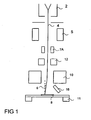
- FIG. 1 A preferred embodiment according to the invention is shown schematically in Fig. 1 .
- the basic components of the device are an electron source 2, a lens system (condenser lens 5 and objective lens 10), scanning coils 12A and 12B, beam shift coils 7 and a detector 16.
- an electron beam 4 is emitted from the electron source 2.
- the electron source may, for example, be a tungsten-hairpin gun, a lanthanum-hexaboride gun, or a field-emission gun.
- the electrons are accelerated by an accelerating voltage supplied to the electron source 2. Since the beam diameter produced directly by the electron source usually is too large to generate a sharp image at high magnification, the electron beam 4 is guided through the condenser lens 5, which demagnifies the beam and leads the electron beam 4 towards a specimen 8.
- the electron beam 4 then enters the field of the deflector 7A which deflects the electron beam 4 away from its path along the optical axis of the objective lens 10.
- the deflector 7A is followed by the scanning coils 12, which are used to move the electron beam 4 in a television-like raster over the surface of the specimen 8.
- the electron beam 4 enters the objective lens 10 that focuses the electron beam 4 onto the specimen 8.
- the objective lens 10 not only focuses the electron beam 4 but also rotates the electron beam 4. However, this effect is not shown, because it is difficult to depict in a two-dimensional drawing and because the skilled person is well aware of this additional effect.
- the electron beam 4 hits the specimen under a predetermined angle of incidence, preferably in the range between 1° and 20° degrees.
- a variety of secondary products such as electrons of different energy, X rays, light, and heat, as well as electrons scattered backward are produced.
- Many of these secondary products and/or the backscattered charged particles are used to produce the image of the specimen and to collect additional data from the specimen.
- a secondary product of major importance to examination or the image formation of specimens are secondary electrons that escape from the specimen 8 at a variety of angles with relatively low energy (3 to 50 eV).
- the secondary and the back scattered electrons reach the detector 16 and are measured.
- the specimen 8 is supported on a stage 11 (specimen support) which is moveable horizontally in all directions, in order to allow the electron beam 4 to reach the target areas on the specimen which are to be examined.
- stage 11 specimen support
- the electron beam does not hit the specimen along the optical axis but it is displaced from the optical axis. Therefore, the stage 11 performs a corresponding movement with the specimen 8 so that the electron beam hits the same area on the specimen that would have been hit if the electron beam had not been deflected by the beam shift coils 7A.
- the stage 11 again moves the specimen 8 to a new position so that the displacement of the beam caused by the tilting of the beam is compensated. Accordingly, any misregistration between the two images can basically be avoided.
- stereo images of a specimen can be produced in a fast and reliable manner without the need for any additional alignments. Accordingly, the additional information, which is contained in stereo images and which is extremely helpful in many cases, can be accessed without causing any additional costs.
- both images of a stereo pair are produced using an oblique angle of incidence.
- the embodiment shown in Fig. 1 uses a pre-lens deflector 7A in order to deflect the electron beam 4.
- the deflection of the electron beam 4 leads to an off-axis path of the beam through the objective lens 10 which gives rise to chromatic aberrations.
- Fig. 2 shows a schematic diagram of an apparatus according to a further embodiment of the present invention. This embodiment is similar to that of Fig. 1 , except for the following.
- the pre-lens deflector 7A has been replaced by an in-lens deflector 7B that is located within the objective lens 10.
- the chromatic aberrations are reduced considerably. The reduction can amount to 50% or more, if the deflector 7B is placed deep inside the field of the objective lens 10 or even partly below the objective lens 10.
- the embodiment shown in Fig. 2 contains a reference target 40 integrated into the stage 11.
- the reference target 40 is used to determine the precise angle of incidence of the electron beam 4 hitting the reference target 40.
- the reference target may contain a repeating structure of lines or trenches which exhibit vertical walls.
- the reference target 40 is integrated into the stage 11.
- the reference target 40 might as well be provided on a separate support, which for example can be rotated in order to bring the reference target 40 within the scanning range of the electron beam 4.
- a heating system (not shown) can be provided for the reference target 40 so that by heating the reference target 40 contaminants present on the surface of the target are evaporated. By heating the reference target from time to time a clean reference target can be guaranteed over long period of time. Accordingly, the down time of the complete system can be reduced.
- FIG. 3 shows a schematic diagram of an apparatus according to a further embodiment of the present invention. This embodiment is similar to that of Fig. 1 and Fig. 2 , except for the following. Instead of using either a pre-lens deflector 7A or an in-lens deflector 7B, the embodiment shown in Fig. 3 uses the pre-lens deflector 7A and the in-lens deflector 7B in combination.
- the chromatic aberrations caused by a first deflector in this example the pre-lens deflector 7A
- a second deflector in this example the in-lens deflector 7B
- the deflections caused by these coils are properly adjusted.
- a pre-lens deflector 7A and an in-lens deflector 7B are used.
- the precise adjustment of the two deflections depends on a number of parameters, for example the chosen angle of incidence, the beam energy, the objective lens current, etc..
- the practice of the invention does not depend on a precise knowledge of these parameters and their effects on the chromatic aberrations caused by the beam deflection.
- the direction of the deflection and the angle of deflection of the pre-lens and the in-lens deflector at which for a preselected angle of incidence minimum aberration is obtained may be extracted experimentally from the resulting images, either from the images of the specimen 8 itself or from images of the reference target 40.
- the combined action of the pre-lens deflector and the in-lens deflector then lead to a resolution in the range of a few nanometers, which is comparable with the resolution that can be achieved without providing an oblique angle of incidence.
- the invention has thus the advantage that large angles of incidence on a specimen can be provided without a reduction in resolution arising from large chromatic aberrations.
- the embodiment shown in Fig. 3 contains an objective lens 10 which is a combination of a magnetic lens 10A and an electrostatic lens 10B.
- the objective lens 10 is a compound magnetic-electrostatic lens.
- the electrostatic part of the compound magnetic-electrostatic lens 10 is an electrostatic retarding lens 10B.
- Using such a compound magnetic-electrostatic lens 10 yields superior resolution at low acceleration energies, such as a few hundred electron volts in case of a SEM. Such low acceleration energies are desirable, especially in modem semiconductor industry, to avoid charging and/or damaging of radiation sensitive specimens.
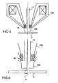
- Figures 4 and 5 show enlarged views on the compound magnetic-electrostatic lens 10 and the specimen 8 as shown in Fig. 3 .
- the magnetic flux generated by a current through an excitation coil is conducted through pole pieces and is concentrated into a small region along the optical axis of the magnetic lens.
- the magnetic field is rotational symmetric around the optical axis and reaches its maximum value in the pole gap between the upper and the lower pole piece.
- the beam shift coils 7B are placed inside the magnetic field of the objective lens 10A, so that there is considerable overlap between their respective fields.
- the embodiment shown in Figs. 3 to 5 contains an electrostatic retarding lens which is situated close to magnetic lens 10A.
- the electrostatic retarding lens 10B has two electrodes held at different potentials. In the illustrated embodiment one of the two electrodes is formed by a cylindrical beam tube 14 which is arranged within the magnetic lens 10A along the optical axis.
- the second electrode of the electrostatic retarding lens 10B is a metallic cup provided below the magnetic lens 10A.
- the first electrode is usually held at high positive potential, for example 8 kV, where as the second electrode is held at lower positive potential, for example 3 kV, so that the electrons are decelerated in the corresponding electrostatic field from a first energy to lower second energy.
- the specimen 8 is held at ground potential. Accordingly, there is a further electrostatic retarding field between the metallic cup and the specimen 8. Due to the electrostatic retarding field between the metallic cup and the specimen 8, an initial deflection of the electron beam 4 caused by the beam shift coils 7A and 7B is enhanced leading to an increased angle of incidence. Accordingly, in order to achieve a predetermined angle of incidence only small deflections caused by the beam shift coils 7A and 7B are necessary.
- the surface of the specimen need not be grounded.
- the electric potential on the surface of the specimen may also be adjusted by applying a voltage to the specimen.
- a voltage can be applied to a wafer, for example, in order to obtain voltage contrast imaging which is used to detect shorts in a circuit. As long as the potential of the metallic cup is higher than the potential on the surface of the specimen, an electrostatic retarding field is produced.
- the stage 11 performs a corresponding movement with the specimen 8 so that the electron beam hits the same area on the specimen that would have been hit, if the electron beam had not been deflected by the beam shift coils 7A.
- the stage 11 again moves the specimen 8 to a new position so that any misregistration between the two images can basically be avoided.
- Fig. 6A and Fig. 6B together with following description will explain how according to the present invention an accurate height measurement is performed.
- Fig. 6A and Fig. 6B show a pillar which extends from a flat surface.
- the distance P1 corresponds to 0.546 ⁇ m whereas the distance P2 corresponds to 0.433 ⁇ m. Accordingly, the height difference Ah between the top of the pillar and the bottom surface in this example is 1.079 ⁇ m.
- Fig. 7A and Fig. 7B show a contact hole extending downward from a flat surface.
- Fig. 7A left view
- Fig. 7B right view
- the left top edge T 1 and the right top edge T 2 can be seen.
- the left bottom edge B R of the contact hole is visible.
- W b T 1 ⁇ B L / cos ⁇ L + T 2 ⁇ B R / cos ⁇ R + h ⁇ tan ⁇ L + tan ⁇ R - W t
- h the depth of the contact hole
- W t the width of the contact hole at the top.
- W t is given by T 1 T 2 /cos ⁇ L .
- the distance T 1 B L /cos ⁇ L corresponds to 0.29 ⁇ m
- the distance T 2 B R /cos ⁇ R corresponds to 0.334 ⁇ m
- the distance T 1 T 2 /cos ⁇ L corresponds to 0.4005 ⁇ m.
- the depth h of the contact hole was determined to be 1.0 ⁇ m. Accordingly, the true width W b of the contact hole at its bottom in this example is 0.324 ⁇ m.
- the method has the advantage that true width W of the contact hole at its bottom can be determined even for contact holes having high aspect ratio (deep and narrow). This is in contrast to other methods, like the atomic force microscopy, which exhibit extreme difficulties in these cases.
- a further embodiment of the present invention can be used, in order to determine the width of a sidewall which is visible in the figures 7A or 7B .
- the width of the left sidewall of the contact hole can be determined.
- the width of the sidewall in this context means the lateral distance in horizontal wafer plane direction between the top of the sidewall and the bottom of the sidewall.
- W L W t - T 2 ⁇ B R / cos ⁇ R - htan ⁇ R
- T 2 B R is the visible distance as measured between the bottom edge of the sidewall and the top edge on the opposite side of the trench or hole
- h is the depth of the trench or hole
- W t is the width of the trench or hole at the top of the trench or the hole
- ⁇ R is the viewing angle of the image of Fig. 7B .
- W R W t - T 1 ⁇ B L / cos ⁇ L - htan ⁇ L
- T 1 B L is the visible distance as measured between the bottom edge of the sidewall and the top edge on the opposite side of the trench or hole
- h is the depth of the trench or hole
- W t is the width of the trench or hole at the top of the trench or the hole
- ⁇ L is the viewing angle of the image of Fig. 7A .
- Fig. 8A the left view, and Fig. 8B , the right view, show a line extending upward from a flat surface.
- Fig. 8A the left bottom edge X 1 , the left top edge X 2 and the right top edge X 3 of the line can be seen.
- Fig. 8B again the left top edge Y 3 and the right top edge Y 2 can be seen.
- the right bottom edge Y 1 of the line is visible.
- W t is given by Y 2 Y 3 /cos ⁇ R .
- the distance (X 1 X 2 + X 2 X 3 )/cos ⁇ L corresponds to 0.274 ⁇ m
- the distance (Y 1 Y 2 + Y 2 Y 3 )/cos ⁇ R corresponds to 0.312 ⁇ m
- the distance Y 2 Y 3 /cos ⁇ R corresponds to 0.232 ⁇ m.
- the depth h of the line was determined to be 0.8 ⁇ m. Accordingly, the true width W b of the line at its bottom in this example is 0.27 ⁇ m.
- this method has the advantage that true width W of the line at its bottom can be determined even for lines having high aspect ratio (high and narrow). This is in contrast to other methods, like the atomic force microscopy, which exhibit extreme difficulties in these cases.
- a further embodiment of the present invention can be used, in order to determine the width of a sidewall which is visible in the figures 8A or 8B .
- the width of the right sidewall of the line can be determined.
- the width of the sidewall in this context means the lateral distance in horizontal direction between the top of the sidewall and the bottom of the sidewall.
- W R Y 1 ⁇ Y 2 / cos ⁇ R - h ⁇ tan ⁇ R
- Y 1 Y 2 is the visible distance as measured between the bottom edge and the top edge of the sidewall of the feature
- h is the height of the feature
- ⁇ R is the viewing angle of the image of Fig 8B .
- W L X 1 ⁇ X 2 / cos ⁇ L - h ⁇ tan ⁇ L
- X 1 X 2 is the visible distance as measured between the bottom edge and the top edge of the sidewall of the feature
- h is the height of the feature
- ⁇ L is the viewing angle of the image of Fig 8A .
- Fig. 9A and Fig. 9B show a top view and a tilt view of a trench present on the surface of a wafer.
- the tilt view makes it possible to see and to define the true character of the sidewall of the trench.
- the sidewall can be seen much better and with significantly more details which are undetectable in Fig. 9A , the top view.
- a sidewall profile of the left sidewall of the trench can be compiled from Fig. 9B .
- the edge in the tilt view captures about twice as many pixels as in the top view. Obviously, this leads to a measurement of the edge width having a significantly better accuracy.
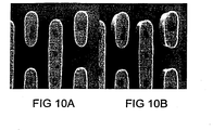
- Fig. 10A and Fig. 10B show a top view and a tilt view of a line present on the surface of a wafer.
- the tilt view ( Fig. 10B ) makes it possible to see and to define the true character of the sidewall of the line.
- the side wall In the tilt view the side wall can be defined as T-top and its profile can be determined.
- the T-top In the top ( Fig. 10A ) the T-top is undetectable.
Landscapes
- Chemical & Material Sciences (AREA)
- Analytical Chemistry (AREA)
- Physics & Mathematics (AREA)
- Electromagnetism (AREA)
- General Physics & Mathematics (AREA)
- Length-Measuring Devices Using Wave Or Particle Radiation (AREA)
- Testing Or Measuring Of Semiconductors Or The Like (AREA)
- Analysing Materials By The Use Of Radiation (AREA)
Description
- The invention relates to a method and a system for the examination of specimen. Especially, the invention relates to a method and a system for the examination of specimen with a beam of charged particles.
- The resolution of the conventional optical microscopy is limited by the wavelength of the visible light. Furthermore, at the highest resolution the conventional optical microscopy has a very shallow depth of field. These two limitations have led to the increased popularity of charged particle devices for the examination of specimen. Compared to optical light accelerated charged particles, for example electrons, do exhibit a shorter wavelength, which leads to an increased resolution power. Accordingly, charged particle beams, especially electron beams, are used in a variety of ways in biology, medicine, the materials sciences, and lithography. Examples include the diagnosis of human, animal, and plant diseases, visualization of sub cellular components and structures such as DNA, determination of the structure of composite materials, thin films, and ceramics, or the inspection of masks and wafers used in semiconductor technology.
- Furthermore, charged particle devices are well suited for the examination of the microstructure of solid surfaces. Especially, the scanning electron microscope is a versatile instrument for examining the microstructure of a surface, because it combines high spatial resolution with depth of field in the same image, and requires only minimal sample preparation. Modem instruments distinguish features as small as 1 nm, while retaining crisp focus throughout tens of microns in the vertical direction. Hence, it is well suited for routine inspections of the intricate surface details of highly integrated circuits. Charged particle devices may, for example, be used in order to monitor the quality of the wafer processing in the semiconductor industry. Thereby, the device is actually located within the production environment, so that problems of the wafer processing are recognized as soon as possible.
- However, conventional charged particle devices are not capable of providing accurate critical dimension, accurate height or accurate edge width measurements without the need of massive manual interference. In order to measure, for example, the height difference between two image points, usually two images are recorded with a defined specimen tilt between the exposures. However, mechanically tilting the specimen leads to a number of disadvantages. Due to mechanical imperfections a lateral movement of the specimen is inevitable which often results in misregistrations between the elements of a stereo image pair. Accordingly, additional alignments are necessary which slow down the process considerably. Furthermore, tilting large specimen, for example a 12 inch semiconductor wafer, requires a very robust and costly mechanical configuration in order to guarantee an adequate resistance of such a stage against vibrations.
- In order to overcome the problems connected with a mechanical tilt of the specimen, it has been proposed to tilt the electron beam electrically in the electron-optical column to procure the same result, see e.g. B.C. Brenton et al. "A DYNAMIC REAL TIME 3-D MEASUREMENT TECHNIQUE FOR IC INSPECTION", Microelectronic Engineering 5 (1986) 541 - 545, North Holland or J.T.L. Thong et al. "In Situ Topography Measurement in the SEM", SCANNING Vol. 14, 65 -72 (1992), FAMS, Inc.. However, the height resolution of the proposed systems lies in the range of 75 to 100 nm, which is not sufficient for the requirements of the semiconductor industry.
- Due to these problems, critical dimension measurements and side wall profiling are often done with an atomic force microscope. However, using an atomic force microscope requires an additional experimental setup which increases the costs significantly and is also very slow. Accordingly, there is a need for a faster and more automated method of examing a specimen which allows accurate critical dimension, accurate height or accurate edge width measurements.
- Methods of analysing a specimen with an electron beam, in which the beam is tilted and the specimen is moved to two positions corresponding to the tilt of the beam so that the beam hits the same region of the sample under two different angles, are known from
JP-A-58/137949 - The present invention provides a method for the examination of specimen with a beam of charged particles according to claim 1. The present invention also provides an apparatus for the examination of specimen that is capable of performing this improved method according to
claim 11. The method provides one or more images of the specimen made with different view angles, so that, compared to a single top view image of the specimen, a lot of additional information about the specimen can be accessed. The different view angles (angles of incidence) are achieved by tilting the beam between the two images and moving the specimen to a new position so that the displacement of the beam caused by the tilting of the beam is compensated. Accordingly, while displaying/recording the second image the beam scans basically over the same area as it has scanned while displaying/recording the first image. - By providing an oblique angle of incidence on the one hand and a corresponding movement of specimen on the other hand, stereo images of a specimen can be produced in a fast and reliable manner without the need for any additional alignments and without the need for excessive image processing. Accordingly, the additional information, which is contained in stereo images and which is extremely valuable in many cases, can be accessed without causing any additional costs.
- The predetermined angle of incidence is achieved by the combined action of deflecting the beam away from the optical axis of an objective and focusing the beam onto the specimen. The deflection is done in at least two steps which are adjusted to each other so that the chromatic aberrations on the surface of the specimen are minimized.
- It has been found by the present inventors that the chromatic aberrations caused by the first step of the deflection can be compensated to a large extent by the second step of the deflection if the two deflections are properly adjusted. The combined action of the two step deflection and focussing of the beam then leads to a resolution in the range of a few nanometers, which is comparable with the resolution that can be achieved without providing an oblique angle of incidence. The invention has thus the advantage that large angles of incidence on a specimen can be provided without a reduction in resolution arising from large chromatic aberrations.
- According to a still further aspect of the present invention, methods are provided that allow an accurate measurement of important distances on the surface of a specimen, especially on the surface on a semiconductor wafer. These methods use a tilted beam of charged particles to get the information in a very fast and reliable manner.
- Some of the above indicated and other more detailed aspects of the invention will be described in the following description and partially illustrated with reference to the figures. Therein:
-
Fig. 1 is a schematic diagram of a charged particle apparatus according to a first embodiment of the present invention. -
Fig. 2 is a schematic diagram of a charged particle apparatus according to a second embodiment of the present invention. -
Fig. 3 is a schematic diagram of a charged particle apparatus according to a third embodiment of the present invention.. -
Fig. 4 is an enlarged view showing the objective lens of the embodiment ofFig. 3 . -
Fig. 5 is an enlarged view ofFig. 4 . -
Fig. 6A and Fig. 6B show a pillar which extends from a flat surface and whose height is to be determined. -
Fig. 7A and Fig. 7B show a contact hole which is extending downward from a flat surface and whose width at its bottom is to be determined. -
Fig. 8A and Fig. 8B show a line which is extending upward from a flat surface and whose width at its bottom is to be determined. -
Fig. 9A and Fig. 9B show a top view and a tilt view of a trench present on the surface of a wafer. -
Fig. 10A and Fig. 10B show a top view and a tilt view of a line present on the surface of a wafer. - Preliminary, it should be appreciated by those skilled in the art that the present invention can be used with any charged particle device. However, for convenience, the invention will be described with respect to its implementation in a scanning electron microscope (SEM). A preferred embodiment according to the invention is shown schematically in
Fig. 1 . The basic components of the device are anelectron source 2, a lens system (condenser lens 5 and objective lens 10), scanning coils 12A and 12B, beam shift coils 7 and adetector 16. In operation anelectron beam 4 is emitted from theelectron source 2. The electron source may, for example, be a tungsten-hairpin gun, a lanthanum-hexaboride gun, or a field-emission gun. The electrons are accelerated by an accelerating voltage supplied to theelectron source 2. Since the beam diameter produced directly by the electron source usually is too large to generate a sharp image at high magnification, theelectron beam 4 is guided through thecondenser lens 5, which demagnifies the beam and leads theelectron beam 4 towards aspecimen 8. - The
electron beam 4 then enters the field of thedeflector 7A which deflects theelectron beam 4 away from its path along the optical axis of theobjective lens 10. Thedeflector 7A is followed by the scanning coils 12, which are used to move theelectron beam 4 in a television-like raster over the surface of thespecimen 8. After the scanning coils 12 theelectron beam 4 enters theobjective lens 10 that focuses theelectron beam 4 onto thespecimen 8. Theobjective lens 10 not only focuses theelectron beam 4 but also rotates theelectron beam 4. However, this effect is not shown, because it is difficult to depict in a two-dimensional drawing and because the skilled person is well aware of this additional effect. - Due to the combined action of the
deflector 7A and theobjective lens 10, theelectron beam 4 hits the specimen under a predetermined angle of incidence, preferably in the range between 1° and 20° degrees. When the electrons strike the surface of thespecimen 8, a variety of secondary products, such as electrons of different energy, X rays, light, and heat, as well as electrons scattered backward are produced. Many of these secondary products and/or the backscattered charged particles are used to produce the image of the specimen and to collect additional data from the specimen. A secondary product of major importance to examination or the image formation of specimens are secondary electrons that escape from thespecimen 8 at a variety of angles with relatively low energy (3 to 50 eV). The secondary and the back scattered electrons reach thedetector 16 and are measured. By scanning the electron beam over the specimen and displaying/recording the output of thedetector 16 an image of the surface of thespecimen 8 is formed. - The
specimen 8 is supported on a stage 11 (specimen support) which is moveable horizontally in all directions, in order to allow theelectron beam 4 to reach the target areas on the specimen which are to be examined. When thespecimen 8 is viewed under an oblique angle of incidence, the electron beam does not hit the specimen along the optical axis but it is displaced from the optical axis. Therefore, thestage 11 performs a corresponding movement with thespecimen 8 so that the electron beam hits the same area on the specimen that would have been hit if the electron beam had not been deflected by the beam shift coils 7A. When the deflection of theelectron beam 4 and, accordingly, the angle of incidence is changed, for example to produce a pair of stereo images, thestage 11 again moves thespecimen 8 to a new position so that the displacement of the beam caused by the tilting of the beam is compensated. Accordingly, any misregistration between the two images can basically be avoided. - By providing an oblique angle of incidence on the one hand and a corresponding movement of specimen on the other hand, stereo images of a specimen can be produced in a fast and reliable manner without the need for any additional alignments. Accordingly, the additional information, which is contained in stereo images and which is extremely helpful in many cases, can be accessed without causing any additional costs. Normally, both images of a stereo pair are produced using an oblique angle of incidence. However, depending on the application, one of the stereo images may also be produced by using a top view of the specimen (θ = 0°).
- The embodiment shown in
Fig. 1 uses apre-lens deflector 7A in order to deflect theelectron beam 4. The deflection of theelectron beam 4 leads to an off-axis path of the beam through theobjective lens 10 which gives rise to chromatic aberrations. - In order to decrease the chromatic aberrations,
Fig. 2 shows a schematic diagram of an apparatus according to a further embodiment of the present invention. This embodiment is similar to that ofFig. 1 , except for the following. Thepre-lens deflector 7A has been replaced by an in-lens deflector 7B that is located within theobjective lens 10. When thedeflector 7B is placed inside the field of theobjective lens 10, the chromatic aberrations are reduced considerably. The reduction can amount to 50% or more, if thedeflector 7B is placed deep inside the field of theobjective lens 10 or even partly below theobjective lens 10. - In order to further improve the performance of system, the embodiment shown in
Fig. 2 contains areference target 40 integrated into thestage 11. Thereference target 40 is used to determine the precise angle of incidence of theelectron beam 4 hitting thereference target 40. For example, the reference target may contain a repeating structure of lines or trenches which exhibit vertical walls. By moving thestage 11 so that thereference target 40 comes within the scanning range of theelectron beam 4, images of thereference target 40 can be used to measure the angle of incidence and to find a parameter setting (for example for thedeflector 7B, theobjective lens 10, the beam energy, etc.) so thatelectron beam 4 hits thereference target 40 with predetermined angle of incidence. Once this parameter setting has been found, it can be used for precise measurements on theactual specimen 8 later on. - In the embodiment shown in
Fig. 2 thereference target 40 is integrated into thestage 11. However, thereference target 40 might as well be provided on a separate support, which for example can be rotated in order to bring thereference target 40 within the scanning range of theelectron beam 4. Furthermore, a heating system (not shown) can be provided for thereference target 40 so that by heating thereference target 40 contaminants present on the surface of the target are evaporated. By heating the reference target from time to time a clean reference target can be guaranteed over long period of time. Accordingly, the down time of the complete system can be reduced. - In order to further decrease the chromatic aberrations,
Fig. 3 shows a schematic diagram of an apparatus according to a further embodiment of the present invention. This embodiment is similar to that ofFig. 1 andFig. 2 , except for the following. Instead of using either apre-lens deflector 7A or an in-lens deflector 7B, the embodiment shown inFig. 3 uses thepre-lens deflector 7A and the in-lens deflector 7B in combination. It has been found by the present inventors that the chromatic aberrations caused by a first deflector, in this example thepre-lens deflector 7A, can be compensated to a large extent by a second deflector, in this example the in-lens deflector 7B, if the deflections caused by these coils are properly adjusted. In the present example apre-lens deflector 7A and an in-lens deflector 7B are used. However, it is also possible to use two pre-lens deflectors or two in-lens deflectors to achieve the same results. - The precise adjustment of the two deflections depends on a number of parameters, for example the chosen angle of incidence, the beam energy, the objective lens current, etc.. However, the practice of the invention does not depend on a precise knowledge of these parameters and their effects on the chromatic aberrations caused by the beam deflection. The direction of the deflection and the angle of deflection of the pre-lens and the in-lens deflector at which for a preselected angle of incidence minimum aberration is obtained may be extracted experimentally from the resulting images, either from the images of the
specimen 8 itself or from images of thereference target 40. The combined action of the pre-lens deflector and the in-lens deflector then lead to a resolution in the range of a few nanometers, which is comparable with the resolution that can be achieved without providing an oblique angle of incidence. The invention has thus the advantage that large angles of incidence on a specimen can be provided without a reduction in resolution arising from large chromatic aberrations. - In order to further improve the performance of system, the embodiment shown in
Fig. 3 contains anobjective lens 10 which is a combination of amagnetic lens 10A and anelectrostatic lens 10B. Accordingly, theobjective lens 10 is a compound magnetic-electrostatic lens. Preferably, the electrostatic part of the compound magnetic-electrostatic lens 10 is anelectrostatic retarding lens 10B. Using such a compound magnetic-electrostatic lens 10 yields superior resolution at low acceleration energies, such as a few hundred electron volts in case of a SEM. Such low acceleration energies are desirable, especially in modem semiconductor industry, to avoid charging and/or damaging of radiation sensitive specimens. -
Figures 4 and 5 show enlarged views on the compound magnetic-electrostatic lens 10 and thespecimen 8 as shown inFig. 3 . To achieve a small focal length, the magnetic flux generated by a current through an excitation coil is conducted through pole pieces and is concentrated into a small region along the optical axis of the magnetic lens. The magnetic field is rotational symmetric around the optical axis and reaches its maximum value in the pole gap between the upper and the lower pole piece. Furthermore, thebeam shift coils 7B are placed inside the magnetic field of theobjective lens 10A, so that there is considerable overlap between their respective fields. - In addition to the
magnetic lens 10A the embodiment shown inFigs. 3 to 5 contains an electrostatic retarding lens which is situated close tomagnetic lens 10A. Theelectrostatic retarding lens 10B has two electrodes held at different potentials. In the illustrated embodiment one of the two electrodes is formed by acylindrical beam tube 14 which is arranged within themagnetic lens 10A along the optical axis. The second electrode of theelectrostatic retarding lens 10B is a metallic cup provided below themagnetic lens 10A. In operation of the system the first electrode is usually held at high positive potential, for example 8 kV, where as the second electrode is held at lower positive potential, for example 3 kV, so that the electrons are decelerated in the corresponding electrostatic field from a first energy to lower second energy. - In the example shown in
Figs 4 and 5 thespecimen 8 is held at ground potential. Accordingly, there is a further electrostatic retarding field between the metallic cup and thespecimen 8. Due to the electrostatic retarding field between the metallic cup and thespecimen 8, an initial deflection of theelectron beam 4 caused by the beam shift coils 7A and 7B is enhanced leading to an increased angle of incidence. Accordingly, in order to achieve a predetermined angle of incidence only small deflections caused by the beam shift coils 7A and 7B are necessary. - The surface of the specimen need not be grounded. The electric potential on the surface of the specimen may also be adjusted by applying a voltage to the specimen. A voltage can be applied to a wafer, for example, in order to obtain voltage contrast imaging which is used to detect shorts in a circuit. As long as the potential of the metallic cup is higher than the potential on the surface of the specimen, an electrostatic retarding field is produced.
- As can be seen from
Fig. 5 , when thespecimen 8 is viewed under an oblique angle of incidence θ, as measured with regard to an axis normal to the surface of the specimen, the electron beam does not hit the specimen along the optical axis of theobjective lens 10. Theelectron beam 4 is displaced from the optical axis by a distance d. Therefore, thestage 11 performs a corresponding movement with thespecimen 8 so that the electron beam hits the same area on the specimen that would have been hit, if the electron beam had not been deflected by the beam shift coils 7A. When the deflection of theelectron beam 4 and, accordingly, the angle of incidence θ is changed, for example to -θ, thestage 11 again moves thespecimen 8 to a new position so that any misregistration between the two images can basically be avoided. -
Fig. 6A and Fig. 6B together with following description will explain how according to the present invention an accurate height measurement is performed.Fig. 6A and Fig. 6B show a pillar which extends from a flat surface.Fig. 6A is an image of the pillar taken with a beam tilt of θL = - 3° whereasFig. 6B is an image of the pillar taken with a beam tilt of θR = + 3° with respect to an axis normal to the flat surface. - To determine the height difference Δh between the top of the pillar and the bottom surface a distinctive feature has to be located for each level. On top of the pillar the right end of a flake was used as the first distinctive feature. On the bottom surface the end of a particle was used as the second distinctive feature. In both images the distance in X-direction between the two features is measured, P1 for
Fig. 6A and P2 forFig. 6B . The difference P between the distance P1 and the distance P2 (P = P1 - P2, P is called the parallax) is then used in order to calculate the height difference Δh between the top of the pillar and the bottom surface. The height difference Δl is given by the formula:
- For small angle approximation (θR, θL ≤ 5°) the height difference can also be given by:

- In the example shown in
Figures 6A and 6B the distance P1 corresponds to 0.546 µm whereas the distance P2 corresponds to 0.433 µm. Accordingly, the height difference Ah between the top of the pillar and the bottom surface in this example is 1.079 µm. - Due to the present invention it does not take any extra effort to gain additional height information from the specimen. However, this additional information is often extremely valuable, particularly on specimens whose topography is complex. In this example the height of a pillar was determined. It is clear, however, that the same procedure can also be used to determine the depth of a trench or a hole. In case of a semiconductor wafer the accurate depth of a trench, for example the depth of an isolation trench, or the accurate depth of a contact hole is extremely useful information in order to control the quality of the production process.
- Once the depth of a trench or a hole or the height of a line is known, this information can be used in order to determine further interesting features. For example, by knowing the depth of a contact hole, a further embodiment of the present invention can be used, in order to determine the true width of the contact hole at its bottom.
Fig. 7A and Fig. 7B show a contact hole extending downward from a flat surface.Fig. 7A is an image of the contact hole taken with a beam tilt of θL = - 3° whereasFig. 7B is an image of the contact hole taken with a beam tilt of θR = + 3° with respect to an axis normal to the flat surface. - In
Fig. 7A (left view) the left top edge T1, the right top edge T2 and the right bottom edge BL of the contact hole can be seen. InFig. 7B (right view) again the left top edge T1 and the right top edge T2 can be seen. Furthermore, the left bottom edge BR of the contact hole is visible. By measuring the visible distances T1BL and T1T2 as measured inFig. 7A , the left view, and the distance T2BR as measured inFig. 7B , the right view, the true width Wb of the contact hole at its bottom can be calculated:
where h is the depth of the contact hole and Wt is the width of the contact hole at the top. In the present example Wt is given by T1T2/cosθL. In the example shown inFigures 7A and 7B the distance T1BL/cosθL corresponds to 0.29 µm, the distance T2BR/cosθR corresponds to 0.334 µm and the distance T1T2/cosθL corresponds to 0.4005 µm. Furthermore, the depth h of the contact hole was determined to be 1.0 µm. Accordingly, the true width Wb of the contact hole at its bottom in this example is 0.324 µm. - The method has the advantage that true width W of the contact hole at its bottom can be determined even for contact holes having high aspect ratio (deep and narrow). This is in contrast to other methods, like the atomic force microscopy, which exhibit extreme difficulties in these cases.
- In addition to the determination of the true width W of the contact hole at its bottom, a further embodiment of the present invention can be used, in order to determine the width of a sidewall which is visible in the
figures 7A or 7B . For example, fromFig. 7B the width of the left sidewall of the contact hole can be determined. The width of the sidewall in this context means the lateral distance in horizontal wafer plane direction between the top of the sidewall and the bottom of the sidewall. By measuring the visible distance T2BR as measured inFig. 7B the true width WL of the left sidewall of the contact hole can be calculated:
where T2BR is the visible distance as measured between the bottom edge of the sidewall and the top edge on the opposite side of the trench or hole, h is the depth of the trench or hole, Wt is the width of the trench or hole at the top of the trench or the hole, and θR is the viewing angle of the image ofFig. 7B . - Similarly, by measuring the visible distance T1BL as measured in
Fig. 7A the true width WR of the left sidewall of the contact hole can be calculated:
where T1BL is the visible distance as measured between the bottom edge of the sidewall and the top edge on the opposite side of the trench or hole, h is the depth of the trench or hole, Wt is the width of the trench or hole at the top of the trench or the hole, and θL is the viewing angle of the image ofFig. 7A . - According to a further embodiment of the present invention, by knowing the height of a line a pair of stereo images of that line can be used in order to determine the true width of the line at its bottom.
Fig. 8A , the left view, andFig. 8B , the right view, show a line extending upward from a flat surface.Fig. 8A is an image of the line taken with a beam tilt of θL = - 3° whereasFig. 8B is an image of the line taken with a beam tilt of θR = + 3° with respect to an axis normal to the flat surface. - In
Fig. 8A the left bottom edge X1, the left top edge X2 and the right top edge X3 of the line can be seen. InFig. 8B again the left top edge Y3 and the right top edge Y2 can be seen. Furthermore, the right bottom edge Y1 of the line is visible. By measuring the visible distances X1X2 and X2X3 as measured inFig. 8A and the visible distances Y1Y2 and Y2Y3 as measured inFig. 8B the true width Wb of the line at its bottom can be calculated:
or
or
where h is the height of the line and Wt is the width of the feature at the top of the feature. For example, Wt is given by Y2Y3/cosθR.. In the example shown inFigures 8A and 8B the distance (X1X2 + X2X3)/cosθL corresponds to 0.274 µm, the distance (Y1Y2 + Y2Y3)/cosθR corresponds to 0.312 µm and the distance Y2Y3/cosθR corresponds to 0.232 µm. Furthermore, the depth h of the line was determined to be 0.8 µm. Accordingly, the true width Wb of the line at its bottom in this example is 0.27 µm. - Instead of the above presented formula, further equivalent formula can also be used, for example:

or
or
- Again, this method has the advantage that true width W of the line at its bottom can be determined even for lines having high aspect ratio (high and narrow). This is in contrast to other methods, like the atomic force microscopy, which exhibit extreme difficulties in these cases.
- In addition to the determination of the true width W of the line at its bottom, a further embodiment of the present invention can be used, in order to determine the the width of a sidewall which is visible in the
figures 8A or 8B . For example, fromFig. 8B the width of the right sidewall of the line can be determined. The width of the sidewall in this context means the lateral distance in horizontal direction between the top of the sidewall and the bottom of the sidewall. By measuring the visible distance Y1Y2 as measured inFig. 8B the true width WR of the right sidewall of the line can be calculated:
where Y1Y2 is the visible distance as measured between the bottom edge and the top edge of the sidewall of the feature, h is the height of the feature, and θR is the viewing angle of the image ofFig 8B . - Similarly, by measuring the visible distance X1X2 as measured in
Fig. 8A the true width WL of the left sidewall of the line can be calculated:
where X1X2 is the visible distance as measured between the bottom edge and the top edge of the sidewall of the feature, h is the height of the feature, and θL is the viewing angle of the image ofFig 8A . -
Fig. 9A and Fig. 9B show a top view and a tilt view of a trench present on the surface of a wafer. As can be seen fromFig. 9B , the tilt view makes it possible to see and to define the true character of the sidewall of the trench. In the tilt view the sidewall can be seen much better and with significantly more details which are undetectable inFig. 9A , the top view. Accordingly, a sidewall profile of the left sidewall of the trench can be compiled fromFig. 9B . Furthermore, by looking at same edge portions in both images, it is easy to see that the edge in the tilt view captures about twice as many pixels as in the top view. Obviously, this leads to a measurement of the edge width having a significantly better accuracy. -
Fig. 10A and Fig. 10B show a top view and a tilt view of a line present on the surface of a wafer. Again, the tilt view (Fig. 10B ) makes it possible to see and to define the true character of the sidewall of the line. In the tilt view the side wall can be defined as T-top and its profile can be determined. In the top (Fig. 10A ) the T-top is undetectable. - While the invention has been described with reference to various exemplary embodiments thereof, those of ordinary skill in the art would appreciate that various implementations and variations are possible without departing from the scope of the invention, as defined by the appended claims. For example, it should be readily apparent that angles and the height and width dimension presented with regard to
Figures 6 to 8 are only examples and that other angles, height and width dimension can be used. Similarly, the configuration of the objective lens is provided as example only, and other configurations of the objective lens may be used.
Claims (24)
- A method for the examination of specimen with a beam of charged particles, said method comprising the steps of:a) scanning the beam over the specimen, to produce a first image, whereby the beam hits the surface of the specimen at a first angle of incidence;b) tilting the beam and moving the specimen to a position corresponding to the tilting of the beam so that the beam hits the surface of the specimen at a second angle of incidence and that the displacement of the beam caused by the tilting of the beam is basically compensated,
wherein the tilting of the beam is achieved by the combined action of deflecting the beam away from the optical axis of an objective and focusing the beam onto the specimen; andc) scanning the beam over the specimen, to produce a second image, whereby the beam hits the surface of the specimen under the second angle of incidence,
characterized in that the deflection of the beam is done inside the field of the objective or in that the beam is deflected in two steps, the first step being done before the beam enters the field of the objective and the second step being done inside the field of the objective. - The method according one of claim 1 wherein the beam is deflected in two steps which are adjusted to each other so that the chromatic aberrations on the surface of the specimen are minimized.
- The method according to one of the preceding claims wherein the two images are used to measure height differences on the specimen.
- The method according to one of claims 1 to 2 wherein the two images are used to measure the width of a feature recessed in the surface of a specimen, such as a trench or a hole, at the bottom of the feature.
- The method according to one of claims 1 to 2 wherein the two images are used to measure the width of a feature protruding from the surface of the specimen at the bottom of the feature.
- The method according to one of claims 1 to 2 wherein the two images are used to compile a stereoscopic image of the surface of the specimen that can be used to produce a 3-dimensional perception.
- The method according to one of claims 1 to 2 wherein the two images are used to produce a 3-dimensional representation of a feature.
- The method according to one of claims 1 to 2 wherein the two images are used to measure the width of an edge of a feature.
- The method according to one of claims 1 to 2 wherein the two images are used to compile a sidewall profile of a feature.
- The method according to one of the preceding claims wherein a reference target is provided in order to determine the precise angle of incidence.
- A charged particle apparatus for the examination of specimen comprising:a) a particle source for providing a beam of charged particles;b) an objective for focusing the charged particle beam onto the specimen;c) a detector for measuring at least one secondary product and/or backscattered particles coming from the specimen;d) at least one deflector for deflecting the beam away from the optical axis of the objective so that by the combined action of the deflector and the objective the beam is tilted and hits the specimen with a predetermined angle of incidence;e) a specimen support for bringing the specimen to position corresponding to the tilt of the beam; andf) a scanning unit for scanning the charged particle beam over the specimen, so that an image is generated;
characterized in that the deflector is located within the field of the objective. - The apparatus according to claim 11 wherein the apparatus comprises two deflectors which are adjusted to each other so that the chromatic aberrations on the surface of the specimen are minimized.
- The apparatus according to claim 12 wherein the first deflector is located before the objective outside the field of the objective and the second deflector is the deflector located within the field of the objective.
- The apparatus according to one of claims 11 to 13 wherein the objective is a combination of a magnetic lens and an electrostatic lens.
- The apparatus according to claim 14 wherein an electrostatic retarding field is provided between the electrostatic lens and the specimen.
- The apparatus according to one of claims 11 to 15 wherein a reference target is provided in order to determine the precise angle of incidence.
- The method according to any of claims 1 to 10, the method further comprising the steps of:providing a beam of charged particles;deflecting the beam away from the optical axis of an objective, said deflection is done in at least two steps which are adjusted to each other so that the chromatic aberrations on the surface of the specimen are minimized; andfocusing the beam onto the surface of the specimen, so that the beam hits the surface of the specimen under the predetermined angle of incidence.
- The method according to claim 17 wherein the first step is done before the beam enters the field of the objective and the second step is done inside the field of the objective.
- The method according to one of claims 17 or 18 wherein the focusing of the beam is done by a combination of a magnetic lens and an electrostatic lens.
- The method according to claim 19 wherein an electrostatic retarding field is provided between the electrostatic lens and the specimen.
- The apparatus according to any of claims 11 to 16, comprising
at least two deflectors for deflecting the beam away from the optical axis of the objective so that by the combined action of the deflectors and the objective the beam is tilted and hits the specimen with a predetermined angle of incidence, said deflectors being adjusted to each other so that the chromatic aberrations on the surface of the specimen are minimized. - The apparatus according to claim 21 wherein a first deflector is located before the objective outside the field of the objective and a second deflector is located within the field of the objective.
- The apparatus according to one of claims 21 or 22 wherein the objective is a combination of a magnetic lens and an electrostatic lens.
- The apparatus according to claim 23 wherein an electrostatic retarding field is provided between the electrostatic lens and the specimen.
Applications Claiming Priority (1)
| Application Number | Priority Date | Filing Date | Title |
|---|---|---|---|
| PCT/EP1999/009926 WO2001045136A1 (en) | 1999-12-14 | 1999-12-14 | Method and system for the examination of specimen using a charged particle beam |
Publications (2)
| Publication Number | Publication Date |
|---|---|
| EP1238405A1 EP1238405A1 (en) | 2002-09-11 |
| EP1238405B1 true EP1238405B1 (en) | 2014-06-18 |
Family
ID=8167527
Family Applications (1)
| Application Number | Title | Priority Date | Filing Date |
|---|---|---|---|
| EP99964573.2A Expired - Lifetime EP1238405B1 (en) | 1999-12-14 | 1999-12-14 | Method and system for the examination of specimen using a charged particle beam |
Country Status (4)
| Country | Link |
|---|---|
| EP (1) | EP1238405B1 (en) |
| JP (1) | JP3916464B2 (en) |
| KR (2) | KR100576940B1 (en) |
| WO (1) | WO2001045136A1 (en) |
Families Citing this family (27)
| Publication number | Priority date | Publication date | Assignee | Title |
|---|---|---|---|---|
| JP2002131252A (en) * | 2000-10-13 | 2002-05-09 | Applied Materials Inc | Method and apparatus for inspecting substrate |
| US6674075B2 (en) * | 2002-05-13 | 2004-01-06 | Applied Materials, Inc. | Charged particle beam apparatus and method for inspecting samples |
| US7223974B2 (en) | 2002-05-22 | 2007-05-29 | Applied Materials, Israel, Ltd. | Charged particle beam column and method for directing a charged particle beam |
| US7800062B2 (en) * | 2002-06-11 | 2010-09-21 | Applied Materials, Inc. | Method and system for the examination of specimen |
| US6930308B1 (en) | 2002-07-11 | 2005-08-16 | Kla-Tencor Technologies Corporation | SEM profile and surface reconstruction using multiple data sets |
| JP4493495B2 (en) * | 2002-07-11 | 2010-06-30 | アプライド マテリアルズ インコーポレイテッド | System and method for determining cross-sectional characteristics of structural elements having submicron cross-sections |
| US6825475B2 (en) | 2002-09-19 | 2004-11-30 | Applied Materials Israel, Ltd. | Deflection method and system for use in a charged particle beam column |
| US7528614B2 (en) | 2004-12-22 | 2009-05-05 | Applied Materials, Inc. | Apparatus and method for voltage contrast analysis of a wafer using a tilted pre-charging beam |
| JP2006514408A (en) * | 2003-02-05 | 2006-04-27 | アプライド マテリアルズ イスラエル リミテッド | Method for measuring and reducing angular displacement of charged particle beams |
| US7034297B2 (en) | 2003-03-05 | 2006-04-25 | Applied Materials, Israel, Ltd. | Method and system for use in the monitoring of samples with a charged particle beam |
| KR101035426B1 (en) | 2003-07-11 | 2011-05-18 | 어플라이드 머티리얼즈 이스라엘 리미티드 | A system and method for determining a cross sectional feature of a structural element using a reference structural element |
| KR101041661B1 (en) | 2003-07-30 | 2011-06-14 | 어플라이드 머티리얼즈 이스라엘 리미티드 | Scanning electron microscope having multiple detectors and a method for multiple detector based imaging |
| US7842933B2 (en) | 2003-10-22 | 2010-11-30 | Applied Materials Israel, Ltd. | System and method for measuring overlay errors |
| US7164128B2 (en) | 2003-11-25 | 2007-01-16 | Hitachi High-Technologies Corporation | Method and apparatus for observing a specimen |
| US7375326B2 (en) * | 2004-06-21 | 2008-05-20 | Applied Materials, Israel, Ltd. | Method and system for focusing a charged particle beam |
| US7112803B2 (en) | 2004-07-23 | 2006-09-26 | Applied Materials, Israel, Ltd. | Beam directing system and method for use in a charged particle beam column |
| KR100595138B1 (en) * | 2004-12-31 | 2006-06-30 | 동부일렉트로닉스 주식회사 | Operating method of atomic force microscope |
| EP1916695B1 (en) | 2006-10-25 | 2018-12-05 | ICT, Integrated Circuit Testing Gesellschaft für Halbleiterprüftechnik mbH | Charged particle beam apparatus and method for operating it |
| US8735030B2 (en) | 2010-04-15 | 2014-05-27 | Carl Zeiss Smt Gmbh | Method and apparatus for modifying a substrate surface of a photolithographic mask |
| JP5735262B2 (en) * | 2010-11-12 | 2015-06-17 | 株式会社日立ハイテクノロジーズ | Charged particle optical apparatus and lens aberration measuring method |
| US9046475B2 (en) | 2011-05-19 | 2015-06-02 | Applied Materials Israel, Ltd. | High electron energy based overlay error measurement methods and systems |
| US9810619B2 (en) | 2012-09-12 | 2017-11-07 | Kla-Tencor Corporation | Method and system for simultaneous tilt and height control of a substrate surface in an inspection system |
| JP6138454B2 (en) | 2012-10-29 | 2017-05-31 | 株式会社日立ハイテクノロジーズ | Charged particle beam equipment |
| JP6640057B2 (en) * | 2016-09-14 | 2020-02-05 | 株式会社日立ハイテクノロジーズ | Electron microscope apparatus and method for measuring inclined hole using the same |
| JP6865465B2 (en) | 2017-11-10 | 2021-04-28 | 株式会社日立ハイテク | Pattern measuring device and measuring method |
| US11177112B2 (en) | 2018-03-19 | 2021-11-16 | Hitachi High-Tech Corporation | Pattern measurement device and non-transitory computer readable medium having stored therein program for executing measurement |
| CN113785170B (en) | 2019-05-08 | 2023-07-14 | 株式会社日立高新技术 | Pattern measuring apparatus and measuring method |
Citations (2)
| Publication number | Priority date | Publication date | Assignee | Title |
|---|---|---|---|---|
| JPS4922768B1 (en) * | 1970-09-11 | 1974-06-11 | ||
| GB1359063A (en) * | 1971-05-14 | 1974-07-10 | Alchem Ltd | Base member for ingot moulds and method for fomring same |
Family Cites Families (19)
| Publication number | Priority date | Publication date | Assignee | Title |
|---|---|---|---|---|
| US3930181A (en) * | 1973-12-28 | 1975-12-30 | Ibm | Lens and deflection unit arrangement for electron beam columns |
| DD126382A1 (en) * | 1976-06-18 | 1977-07-13 | ||
| JPS5434673A (en) * | 1977-08-23 | 1979-03-14 | Hitachi Ltd | Micro-distance measuring device for scan-type electronic microscope |
| JPS54107254A (en) * | 1978-02-10 | 1979-08-22 | Hitachi Ltd | Scanning-type electron microscope |
| GB2067348B (en) * | 1980-01-11 | 1983-10-05 | Zeiss Jena Veb Carl | Deflecting objective for corpuscular radiation apparatus |
| US4376249A (en) * | 1980-11-06 | 1983-03-08 | International Business Machines Corporation | Variable axis electron beam projection system |
| JPS58137949A (en) * | 1982-02-10 | 1983-08-16 | Jeol Ltd | Method of displaying three-dimensional image by means of scanning electron microscope |
| JPS59171445A (en) * | 1983-03-18 | 1984-09-27 | Hitachi Ltd | Stereoscopic scanning electron microscope |
| JPS6161002A (en) * | 1984-09-03 | 1986-03-28 | Hitachi Ltd | Automatic measuring system of sectional shape |
| ATE91822T1 (en) * | 1986-04-24 | 1993-08-15 | Integrated Circuit Testing | ELECTROSTATIC-MAGNETIC LENS FOR CORPUSCULAR BLASTING DEVICES. |
| JPH0663758B2 (en) * | 1987-10-14 | 1994-08-22 | 株式会社東芝 | Pattern measurement method |
| US4926054A (en) * | 1988-03-17 | 1990-05-15 | Ict Integrated Circuit Testing Gesellschaft Fur Halbleiterpruftechnik Mbh | Objective lens for focusing charged particles in an electron microscope |
| JPH01311551A (en) * | 1988-06-08 | 1989-12-15 | Toshiba Corp | Pattern shape measuring device |
| JPH0233843A (en) * | 1988-07-25 | 1990-02-05 | Hitachi Ltd | Scanning electronic microscope |
| US5644132A (en) * | 1994-06-20 | 1997-07-01 | Opan Technologies Ltd. | System for high resolution imaging and measurement of topographic and material features on a specimen |
| JPH10302703A (en) * | 1997-04-24 | 1998-11-13 | Hitachi Ltd | Magnification and inclination angle measurement method |
| WO1999034397A1 (en) * | 1997-12-23 | 1999-07-08 | Koninklijke Philips Electronics N.V. | Sem provided with an electrostatic objective and an electrical scanning device |
| JP2909061B2 (en) * | 1998-05-15 | 1999-06-23 | 株式会社日立製作所 | Cross section observation device |
| US6452175B1 (en) * | 1999-04-15 | 2002-09-17 | Applied Materials, Inc. | Column for charged particle beam device |
-
1999
- 1999-12-14 JP JP2001545339A patent/JP3916464B2/en not_active Expired - Lifetime
- 1999-12-14 WO PCT/EP1999/009926 patent/WO2001045136A1/en active IP Right Grant
- 1999-12-14 KR KR1020047019515A patent/KR100576940B1/en active IP Right Grant
- 1999-12-14 KR KR10-2002-7007587A patent/KR100489911B1/en active IP Right Grant
- 1999-12-14 EP EP99964573.2A patent/EP1238405B1/en not_active Expired - Lifetime
Patent Citations (2)
| Publication number | Priority date | Publication date | Assignee | Title |
|---|---|---|---|---|
| JPS4922768B1 (en) * | 1970-09-11 | 1974-06-11 | ||
| GB1359063A (en) * | 1971-05-14 | 1974-07-10 | Alchem Ltd | Base member for ingot moulds and method for fomring same |
Also Published As
| Publication number | Publication date |
|---|---|
| EP1238405A1 (en) | 2002-09-11 |
| KR100576940B1 (en) | 2006-05-10 |
| KR20040107530A (en) | 2004-12-20 |
| KR100489911B1 (en) | 2005-05-17 |
| KR20020061641A (en) | 2002-07-24 |
| JP2003517199A (en) | 2003-05-20 |
| JP3916464B2 (en) | 2007-05-16 |
| WO2001045136A1 (en) | 2001-06-21 |
Similar Documents
| Publication | Publication Date | Title |
|---|---|---|
| EP1238405B1 (en) | Method and system for the examination of specimen using a charged particle beam | |
| US6747279B2 (en) | Objective lens for a charged particle beam device | |
| KR100382026B1 (en) | Scanning Electron Microscope | |
| JP3456999B2 (en) | Detection system for high aspect ratio measurement | |
| JP4914604B2 (en) | Pattern defect inspection method and system using electron beam inspection apparatus, and mapping projection type or multi-beam type electron beam inspection apparatus | |
| JP3996774B2 (en) | Pattern defect inspection method and pattern defect inspection apparatus | |
| US7385198B2 (en) | Method and apparatus for measuring the physical properties of micro region | |
| JP5302595B2 (en) | Inclination observation method and observation apparatus | |
| US7800062B2 (en) | Method and system for the examination of specimen | |
| JP2004014485A (en) | Wafer defect inspection method and wafer defect inspection device | |
| JP2004513477A (en) | SEM with adjustable final electrode for electrostatic objective | |
| US6717144B2 (en) | Scanning electron microscope system | |
| US8008629B2 (en) | Charged particle beam device and method for inspecting specimen | |
| JP2001148232A (en) | Scanning electron microscope | |
| WO1996008835A1 (en) | Particle beam detector providing z-axis and topographic contrast | |
| JP2006128146A (en) | Device and column for test piece inspection | |
| JP2001143649A (en) | Scanning electron microscope | |
| JPH10208683A (en) | Scanning electron microscope | |
| JP2003203597A (en) | Scanning electron microscope | |
| JPH11223522A (en) | Method and apparatus for measuring and inspecting size of structure |
Legal Events
| Date | Code | Title | Description |
|---|---|---|---|
| PUAI | Public reference made under article 153(3) epc to a published international application that has entered the european phase |
Free format text: ORIGINAL CODE: 0009012 |
|
| 17P | Request for examination filed |
Effective date: 20020614 |
|
| AK | Designated contracting states |
Kind code of ref document: A1 Designated state(s): AT BE CH CY DE DK ES FI FR GB GR IE IT LI LU MC NL PT SE |
|
| RIN1 | Information on inventor provided before grant (corrected) |
Inventor name: ADAMEC, PAVEL Inventor name: HAAS, NADAV Inventor name: PETROV, IGOR Inventor name: PEARL, ASHER Inventor name: BEN-AV, RADEL Inventor name: GOLDENSHTEIN, ALEX |
|
| 17Q | First examination report despatched |
Effective date: 20060803 |
|
| GRAP | Despatch of communication of intention to grant a patent |
Free format text: ORIGINAL CODE: EPIDOSNIGR1 |
|
| INTG | Intention to grant announced |
Effective date: 20140109 |
|
| GRAS | Grant fee paid |
Free format text: ORIGINAL CODE: EPIDOSNIGR3 |
|
| GRAA | (expected) grant |
Free format text: ORIGINAL CODE: 0009210 |
|
| AK | Designated contracting states |
Kind code of ref document: B1 Designated state(s): AT BE CH CY DE DK ES FI FR GB GR IE IT LI LU MC NL PT SE |
|
| RAP1 | Party data changed (applicant data changed or rights of an application transferred) |
Owner name: APPLIED MATERIALS, INC. |
|
| REG | Reference to a national code |
Ref country code: GB Ref legal event code: FG4D |
|
| REG | Reference to a national code |
Ref country code: CH Ref legal event code: EP |
|
| REG | Reference to a national code |
Ref country code: AT Ref legal event code: REF Ref document number: 673781 Country of ref document: AT Kind code of ref document: T Effective date: 20140715 |
|
| REG | Reference to a national code |
Ref country code: IE Ref legal event code: FG4D |
|
| REG | Reference to a national code |
Ref country code: DE Ref legal event code: R096 Ref document number: 69945119 Country of ref document: DE Effective date: 20140724 |
|
| REG | Reference to a national code |
Ref country code: NL Ref legal event code: T3 |
|
| PG25 | Lapsed in a contracting state [announced via postgrant information from national office to epo] |
Ref country code: CY Free format text: LAPSE BECAUSE OF FAILURE TO SUBMIT A TRANSLATION OF THE DESCRIPTION OR TO PAY THE FEE WITHIN THE PRESCRIBED TIME-LIMIT Effective date: 20140618 Ref country code: FI Free format text: LAPSE BECAUSE OF FAILURE TO SUBMIT A TRANSLATION OF THE DESCRIPTION OR TO PAY THE FEE WITHIN THE PRESCRIBED TIME-LIMIT Effective date: 20140618 Ref country code: GR Free format text: LAPSE BECAUSE OF FAILURE TO SUBMIT A TRANSLATION OF THE DESCRIPTION OR TO PAY THE FEE WITHIN THE PRESCRIBED TIME-LIMIT Effective date: 20140919 |
|
| REG | Reference to a national code |
Ref country code: AT Ref legal event code: MK05 Ref document number: 673781 Country of ref document: AT Kind code of ref document: T Effective date: 20140618 |
|
| PG25 | Lapsed in a contracting state [announced via postgrant information from national office to epo] |
Ref country code: SE Free format text: LAPSE BECAUSE OF FAILURE TO SUBMIT A TRANSLATION OF THE DESCRIPTION OR TO PAY THE FEE WITHIN THE PRESCRIBED TIME-LIMIT Effective date: 20140618 |
|
| PG25 | Lapsed in a contracting state [announced via postgrant information from national office to epo] |
Ref country code: ES Free format text: LAPSE BECAUSE OF FAILURE TO SUBMIT A TRANSLATION OF THE DESCRIPTION OR TO PAY THE FEE WITHIN THE PRESCRIBED TIME-LIMIT Effective date: 20140618 Ref country code: PT Free format text: LAPSE BECAUSE OF FAILURE TO SUBMIT A TRANSLATION OF THE DESCRIPTION OR TO PAY THE FEE WITHIN THE PRESCRIBED TIME-LIMIT Effective date: 20141020 |
|
| PG25 | Lapsed in a contracting state [announced via postgrant information from national office to epo] |
Ref country code: AT Free format text: LAPSE BECAUSE OF FAILURE TO SUBMIT A TRANSLATION OF THE DESCRIPTION OR TO PAY THE FEE WITHIN THE PRESCRIBED TIME-LIMIT Effective date: 20140618 |
|
| REG | Reference to a national code |
Ref country code: DE Ref legal event code: R097 Ref document number: 69945119 Country of ref document: DE |
|
| PLBE | No opposition filed within time limit |
Free format text: ORIGINAL CODE: 0009261 |
|
| STAA | Information on the status of an ep patent application or granted ep patent |
Free format text: STATUS: NO OPPOSITION FILED WITHIN TIME LIMIT |
|
| PG25 | Lapsed in a contracting state [announced via postgrant information from national office to epo] |
Ref country code: IT Free format text: LAPSE BECAUSE OF FAILURE TO SUBMIT A TRANSLATION OF THE DESCRIPTION OR TO PAY THE FEE WITHIN THE PRESCRIBED TIME-LIMIT Effective date: 20140618 Ref country code: DK Free format text: LAPSE BECAUSE OF FAILURE TO SUBMIT A TRANSLATION OF THE DESCRIPTION OR TO PAY THE FEE WITHIN THE PRESCRIBED TIME-LIMIT Effective date: 20140618 |
|
| 26N | No opposition filed |
Effective date: 20150319 |
|
| PG25 | Lapsed in a contracting state [announced via postgrant information from national office to epo] |
Ref country code: BE Free format text: LAPSE BECAUSE OF FAILURE TO SUBMIT A TRANSLATION OF THE DESCRIPTION OR TO PAY THE FEE WITHIN THE PRESCRIBED TIME-LIMIT Effective date: 20140618 |
|
| PG25 | Lapsed in a contracting state [announced via postgrant information from national office to epo] |
Ref country code: LU Free format text: LAPSE BECAUSE OF FAILURE TO SUBMIT A TRANSLATION OF THE DESCRIPTION OR TO PAY THE FEE WITHIN THE PRESCRIBED TIME-LIMIT Effective date: 20141214 |
|
| REG | Reference to a national code |
Ref country code: CH Ref legal event code: PL |
|
| GBPC | Gb: european patent ceased through non-payment of renewal fee |
Effective date: 20141214 |
|
| REG | Reference to a national code |
Ref country code: IE Ref legal event code: MM4A |
|
| REG | Reference to a national code |
Ref country code: FR Ref legal event code: ST Effective date: 20150831 |
|
| PG25 | Lapsed in a contracting state [announced via postgrant information from national office to epo] |
Ref country code: IE Free format text: LAPSE BECAUSE OF NON-PAYMENT OF DUE FEES Effective date: 20141214 Ref country code: CH Free format text: LAPSE BECAUSE OF NON-PAYMENT OF DUE FEES Effective date: 20141231 Ref country code: GB Free format text: LAPSE BECAUSE OF NON-PAYMENT OF DUE FEES Effective date: 20141214 Ref country code: LI Free format text: LAPSE BECAUSE OF NON-PAYMENT OF DUE FEES Effective date: 20141231 |
|
| PG25 | Lapsed in a contracting state [announced via postgrant information from national office to epo] |
Ref country code: FR Free format text: LAPSE BECAUSE OF NON-PAYMENT OF DUE FEES Effective date: 20141231 |
|
| PG25 | Lapsed in a contracting state [announced via postgrant information from national office to epo] |
Ref country code: MC Free format text: LAPSE BECAUSE OF FAILURE TO SUBMIT A TRANSLATION OF THE DESCRIPTION OR TO PAY THE FEE WITHIN THE PRESCRIBED TIME-LIMIT Effective date: 20140618 |
|
| PGFP | Annual fee paid to national office [announced via postgrant information from national office to epo] |
Ref country code: NL Payment date: 20181123 Year of fee payment: 20 |
|
| PGFP | Annual fee paid to national office [announced via postgrant information from national office to epo] |
Ref country code: DE Payment date: 20181126 Year of fee payment: 20 |
|
| REG | Reference to a national code |
Ref country code: DE Ref legal event code: R071 Ref document number: 69945119 Country of ref document: DE |
|
| REG | Reference to a national code |
Ref country code: NL Ref legal event code: MK Effective date: 20191213 |