JP2004014485A - Wafer defect inspection method and wafer defect inspection device - Google Patents
Wafer defect inspection method and wafer defect inspection device Download PDFInfo
- Publication number
- JP2004014485A JP2004014485A JP2002170796A JP2002170796A JP2004014485A JP 2004014485 A JP2004014485 A JP 2004014485A JP 2002170796 A JP2002170796 A JP 2002170796A JP 2002170796 A JP2002170796 A JP 2002170796A JP 2004014485 A JP2004014485 A JP 2004014485A
- Authority
- JP
- Japan
- Prior art keywords
- sample
- electron beam
- image
- electron
- irradiation
- Prior art date
- Legal status (The legal status is an assumption and is not a legal conclusion. Google has not performed a legal analysis and makes no representation as to the accuracy of the status listed.)
- Granted
Links
Images


Landscapes
- Length-Measuring Devices Using Wave Or Particle Radiation (AREA)
- Analysing Materials By The Use Of Radiation (AREA)
- Testing Or Measuring Of Semiconductors Or The Like (AREA)
Abstract
Description
【0001】
【発明の属する技術分野】
本発明は、試料(半導体装置等)の表面状態を検査する方法および装置に関する。
【0002】
【従来の技術】
半導体装置の製造過程において、ウエハ上に形成された回路パターンの欠陥を画像の比較検査により検出する方法として、点状に絞った電子ビーム(point electron beam)を走査(scanning)するいわゆるSEM方式によるパターンの比較検査方法が、「特開昭59−192943号公報」、「J. Vac. Sci. Tech. B、Vol.9、No.6、pp.3005−3009 (1991)」、「J. Vac. Sci. Tech. B、Vol.10、No.6、pp.2804−2808 (1992)、SPIEVol.2439、 pp.174−183」、および「特開平05−258703号公報」等に記載されている。
【0003】
これらの技術は、光学顕微鏡の分解能以下となる微小なエッチング残りや微小パターン欠陥検出や微小導通孔の非開口不良等の電気的な欠陥の検出に活用されている。これらの技術では、実用的な検査速度を得るために非常に高速にパターンの画像を取得する必要が有る。そして、高速で取得した画像のS/N比( signal to noise ratio)を確保するために、通常の走査型電子顕微鏡の100倍以上(10nA以上)のビーム電流を用いている。
【0004】
さらに、「特開平7−249393号公報」、「特開平10−1974627号公報」、特開2000−340160号公報」、「特開平11−108864号公報」等には、矩形状(rectangulater)の電子ビームを半導体ウエハに照射して反射電子(back scattered electron)や二次電子(secondary electron)または逆電界(retarding field for primary beam )の形成によりウエハに照射(impinge?)されずに反射される(reflect)電子をレンズにより結像させる等、いわゆるプロジェクション方式により高速に検査する装置について記載されている。
【0005】
また、試料に電位を与えて電子ビームが照射されずに表面近くで電界により反射(reflect)される状況を作り出し、試料最表面の画像を取得する技術としてはミラー顕微鏡として知られている(例えば、「Rheinhold Godehardt、ADVANCES IN IMAGING AND ELECTRON PHYSICS、VOL.94、p.81−150」)。
【0006】
【発明が解決しようとする課題】
上記の電子ビームを用いた従来の検査技術では、SEM方式、反射電子や二次電子のプロジェクション方式はいずれも下記の課題が残っていた。
【0007】
まず、SEM方式に関しては検査可能なS/N比を維持した画像を形成するために、電子ビームを一般のSEMよりも大電流化している。しかし、電子ビームを点状に絞ってこの「点ビーム」を試料表面上で平面(2次元的)に走査しているがために高速化(検査時間の短縮)には限界があった。
【0008】
また、採用する電子源の輝度や空間電荷効果(coulomb effect)等によって、電子ビームの大電流化にも限界がある。例えば、0.1μm程度の分解能を得ようとした場合は、電子ビーム電流は数百nA程度が理論限界であり、実際には100nA程度が用いられ得るに過ぎない。画像のS/N比は、画像を形成するのに用いられる電子の数、すなわち、ビーム電流値と画像取得に要する時間との積により決まる。画像処理が正常に動作できる画像のS/N比を確保するにはビーム電流値が100nAで0.1μmの場合、試料表面の面積1cm2を検査するのに100sec以上を必要とする。
【0009】
一方、プロジェクション方式では、SEM方式よりも大電流の電子ビームを一度に照射でき、かつ一括で画像を取得できるためSEM方式と比較して超高速に画像を形成できることが期待できる。ところが、二次電子の放出角度分布は広い角度に広がっており、しかもエネルギーも約1〜10eVと広がっている。このような電子を結像して試料の拡大像を形成するとき大部分の二次電子をカットしないと十分な分解能が得られないことが、「LSIテスティングシンポジウム/1999会議録、P142」に記載の図6から容易に判断することができる。これは試料から放出した二次電子を加速するための負の試料印加電圧と二次電子の結像分解能を示したものである。これによると試料印加電圧−5kVのとき分解能はほぼ0.2μmである。
【0010】
そして、放出した二次電子がすべて画像形成に使用できるわけではなく、たとえば当該引用文献の計算では対物レンズ通過後の像面において1.1mradの開き角以下のビームを使用した場合となっている。この開き角の範囲内の二次電子は全体のたかだか10%程度である。さらに結像に使用する二次電子のエネルギーの幅を1eVで計算しているが、放出される二次電子のエネルギー幅は実際には数eV以上の幅を持って放出しており、高エネルギー側の裾野はおよそ50eVまで存在する。そのような幅広いエネルギー分布を持つ二次電子のうち、たかだか1eVのエネルギー幅のもののみを抽出した場合はさらに数分の一になってしまう。
【0011】
このように、電子ビームを面積ビームとして大電流を照射して一括で画像を形成しようとしても実際に画像形成に寄与できる電子の割合が低いために画像のS/N比を確保することが困難となり結局期待できるほどの検査時間の短縮は不可能である。反射電子を用いる場合も同様に照射ビーム電流に比べて二桁少ない放出量しか得られず、二次電子の場合と同様に高分解能と高速性の両立は困難である。
【0012】
また、先に述べたミラー顕微鏡技術については、この技術を半導体ウエハの検査に適用する手法や装置に関してはこれまで報告がなかった。また、試料に向けられる電子ビームの軌道の方向性に関する制約がなく、広い角度をもって電子ビームが試料に照射されるため分解能がサブμm程度と現状の半導体を観察するには分解能が不充分であった。
【0013】
本発明は、上述の点に着目してなされたものであり、ウエハ上に形成されたパターンにおける欠陥部分を、高分解能でかつ高速で検出する欠陥検査方法及び欠陥検査装置を提供することを目的とする。
【0014】
【課題を解決するための手段】
本発明の目的は、以下の方法で達成できる。
【0015】
すなわち、試料表面の複数の照射領域(面積領域)に、電子ビームを「点ビーム(point beam)」としてではなく2次元的な広がりを持った「面積ビーム(seat beam)」(面状の電子ビーム)として順次照射する。ウエハには負の電位を印加する。この負の電位は、ウエハの最表面付近で大部分の電子ビームが戻される程度の値とする。具体的には電子源(cathode またはelectron source)の電位よりも0.5V〜5V高い負の電位とする。これにより引き戻された電子を結像させる(以降、試料に衝突せずに電界により引き戻された電子を「引き戻された電子」または「ミラー電子」と呼ぶことにする。)。そして、上記複数の照射領域の拡大像を順次形成し、これら複数の照射領域の拡大像を電気的な画像信号に変換して、上記複数の照射領域についての画像信号同士を比較する。これにより上記各照射領域についてのパターン欠陥を高分解能でかつ高速に検出することが可能となる。
【0016】
本発明の代表的な構成例を挙げると、先ず、本発明によるパターン欠陥検査方法は、2次元的な広がりを有する面状の電子ビームを、負の電位を印加された試料表面の複数の照射領域に順次照射し、前記試料に衝突せずに前記試料の表面付近で引き戻された電子を結像せしめて、前記複数の照射領域の拡大電子像を順次形成し、形成された前記複数の照射領域の拡大電子像を電気的な画像信号に変換して、前記複数の照射領域についての画像信号同士を比較することにより、前記試料に形成されたパターン欠陥を検出するよう構成したことを特徴とする。ここで、前記面状の電子ビームは、前記試料表面に対して進行方向を略平行にそろえ略垂直に入射するようにして、前記複数の照射領域の各々を照射するよう構成される。
【0017】
また、本発明によるウェハ欠陥検査装置は、電子源からの電子ビームを2次元的な広がりを有する面状の電子ビームとして試料表面の複数の照射領域に照射する第1の電子光学系と、前記試料に向けて照射した前記電子ビームを形成する電子が前記試料の最表面付近で引き戻されるような電界を発生させるための手段と、前記複数の照射領域から引き戻された電子を結像させて前記複数の照射領域の拡大像を形成するための第2の電子光学系と、前記複数の照射領域の拡大像をそれぞれ電気的な画像信号に変換して検出する画像信号検出手段と、検出された前記試料表面の複数の照射領域の画像信号同士を比較して各照射領域におけるパターン欠陥を検出するための画像信号処理手段とを有し、前記試料に形成されたパターン欠陥を検出するよう構成したことを特徴とする。
【0018】
また、本発明によるパターン欠陥検査装置は、電子源からの電子ビームを2次元的な広がりを有する面状の電子ビームとして試料表面の複数の照射領域に照射する電子ビーム照射光学系と、前記面状の電子ビームを形成する電子の全てもしくは一部が前記試料の表面に衝突する直前で引き戻されるような電界を生じさせる手段と、前記複数の照射領域から引き戻された電子を結像させて前記複数の照射領域の拡大像を形成するための結像光学系と、前記試料を載置して前記複数の照射領域の各々に前記電子ビームが照射されるように前記試料を移動させるための試料移動ステージと、前記複数の照射領域の拡大像の各々を電気的な画像信号に変換して検出する画像信号検出手段と、検出された前記試料表面の複数の照射領域の画像信号同士を比較し、所定の閾値を上回る相違が存在するか否かを判定して各照射領域におけるパターン欠陥を検出する画像信号処理手段とを有してなることを特徴とする。
【0019】
また、本発明によるパターン欠陥検査装置は、前記試料移動ステージの移動方向の所定位置に、試料のSEM画像を取得するための電子光学系を設けてなることを特徴とする。
【0020】
前記第1の電子光学系または電子ビーム照射光学系は、電子ビームを発生する電子銃と、前記電子銃から放出した電子ビームを集束するコンデンサレンズと、前記コンデンサレンズと試料との間に配置された対物レンズと、電子ビーム偏向機構とを有し、前記コンデンサレンズによって前記対物レンズの電子源側の焦点面に前記電子ビームの焦点を配置して、前記試料表面に対して進行方向を略平行にそろえ略垂直に入射する面状の電子ビームを形成し、前記試料表面の複数の照射領域に照射するよう構成する。
また、試料に対向する円孔電極(aperture electrode)が電子レンズとして大きく作用する場合には、前記対物レンズによって、円孔レンズ(aperture lens)の焦点面(focal plane)に前記電子ビームの焦点を配置すれば、前記試料表面に対して進行方向を略平行にそろえ略垂直に入射する面状の電子ビームを形成することができる。
【0021】
試料に向けて照射した電子が試料最表面で引き戻されるような電界を発生させるための前記手段は、たとえば試料を保持する導電性の試料ホルダに所定の負電位を印加する電源で構成される。また、表面に絶縁膜を有する半導体等の試料においては、画像構成用の電子ビームの光軸から離れた場所に第2の電子銃を備え、画像形成前に試料に電子を照射する予備帯電制御手段を備える。さらに、試料と第2の電子銃の間に電位を印加できるグリッドを備え、そのグリッドに印加する電圧を制御しながら第2の電子銃を用いて試料に電子を照射する手段を備える。
半導体試料のパターンのショート、断線などの導通不良を検査するためには、この予備照射により生じる正常パターンと欠陥パターン間の電圧差を検出して不良パターンを検出することが可能となる。しかし、欠陥パターンの抵抗が比較的小さい場合には蓄積した電荷が周りへ逃げてしまうので、予備照射で生じた正常パターンと欠陥パターンとの電位差は長時間保持されない。この場合には、試料に電子を注入して正常パターンと欠陥パターンとの電位差を発生させる手段と試料に当たらずに反射して結像する電子をほぼ同じ場所でほぼ同時に照射する手段を設けることが必要となる。不良パターンおよび絶縁膜パターンを負に帯電させる要求に対しては、試料電位に対してeVnだけ余分なエネルギーの電子ビームを試料に照射して、絶縁物が負電圧Vnに帯電して安定する条件で画像を取得すれば、不良パターンおよび絶縁物パターンを負に帯電させた状態で画像を取得することができる。また、不良パターンおよび絶縁膜パターンを正に帯電させる要求には、画像を取得するビームと試料を正に帯電させるための電子ビームや光を同時、あるいは交互に照射することにより解決される。
【0022】
また、試料移動ステージ(sample stage)は、試料をほぼ等速度で連続的に移動させるよう設定することにより欠陥検査の高速化が実現できる。この場合、試料移動ステージの位置をモニタすることによって、試料表面への電子ビーム照射領域が所定時間、同一箇所となるよう制御する必要があることは云うまでもない。すなわち、連続移動する前記試料移動ステージの位置をリアルタイムに計測するステージ位置計測機構を備え、かつ、連続移動に伴い前記ステージ移動中に発生する位置変動を前記ステージ位置計測機構により測定し、前記電子ビーム照射光学系の前記電子ビーム偏向機構にフィードバックするようにして、前記電子ビームと前記試料との位置関係が、所定の方向にほぼ等速に移動するように構成する。
【0023】
また、前記画像信号検出手段は、前記第2の電子光学系または結像光学系によって結像形成された照射領域の拡大電子像を蛍光板上(phosphor screen)に投射することによって光学像(optical image)に変換し、この光学像を光学レンズまたは光ファイバーを介して光学画像検出素子上に結像させる。または、上記光学系で結像された拡大電子像を電子感応性(sensitivity for electron)を有する画像検出素子上に直接結像させるようにしてもよい。なお、画像検出素子としては、電荷結合型素子(CCD)、または時間遅延して入力した光信号を積分し出力する素子(TDI:Time Delayed Integration sensor)を用いることができる。また、画像検出素子からの検出信号の読み出しは、並列に多チャンネルで読み出す方式とする。
【0024】
【発明の実施の形態】
以下に、本発明の実施例について、図面を参照して詳細に説明する。
【0025】
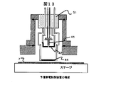
(実施例1)
図1に、本発明の動作原理を説明するために必要な最低限の構成要素を示したものである。電子源1より放出された電子ビームは、コンデンサレンズ2により収束されビームセパレータ3の周辺で、かつ対物レンズの前焦点面にクロスオーバ(crossover)を形成する。電子ビームは、ビームセパレータ3によりウェハ7に垂直な光軸に偏向される。ビームセパレータ3は上方からの電子ビームに対してのみ偏向作用を持つ。たとえば、電場と磁場を直行させたE×B偏向器を用いる。ビームセパレータ3により偏向された電子ビームは、対物レンズ6により試料(ウェハ)表面に垂直な方向にそろった面状の電子ビームが形成される。
【0026】
試料(ウェハ)7には、電子ビームの加速電圧とほぼ等しいか、わずかに高い負の電位が電源9によって印加されており、ウェハ7の表面には形成された半導体パターン形状や帯電の状態を反映した電界が形成されている。この電界によって面状電子ビームの大部分がウェハ7に衝突する直前で引き戻され、ウェハ7のパターン情報を反映した方向や強度を持って上がってくる。
【0027】
引き戻された電子ビームは、対物レンズ6により収束作用を受け、ビームセパレータ3は下方から進行した電子ビームに対しては偏向作用を持たないのでそのまま垂直に上昇し、結像レンズ11により画像検出部103上にウェハ7表面の画像を結像させる。これにより、ウェハ7表面の局部的な帯電電位の変化や凹凸等の構造の違いが画像として形成される。この画像は電気信号に変換され画像処理部104に送られる。
【0028】
ウェハ7に形成された半導体パターンの欠陥を検出するためには、画像処理部104により周辺の同一形状パターン部との画像比較や、あらかじめ取得された無欠陥部の画像との比較を行い、異なっている場所を欠陥として記憶する。ウェハ7はステージ(図示せず)に載置されており、ステージはステージ制御系30により連続的に移動される。ステージ制御系30とビーム制御系28は連動しており、ステージの移動に伴って電子ビームの位置を偏向器(図示せず)により微調整しながら画像取得領域を連続的に移動させていく。
【0029】
ウェハ7の表面に絶縁物が存在する場合には、電源9だけではウェハ7の表面電位を決定できない。そのために、ウェハ表面の電位を所望の電位に帯電させるための機能として予備帯電制御装置32を備えている。ウェハ7表面に近接したグリッド電極へ電圧を印加しつつ電子ビームをウェハ7に照射することでウェハ7の表面の帯電電位を制御する装置である。その動作原理と構造については後述する。ウェハ7の表面を検査前にあらかじめ帯電させる場合には、この予備帯電制御装置32の下を通過させて検査領域を所望の帯電電圧に設定した後に対物レンズ6の直下を通過させて画像を取得するようにする。
【0030】
次に、ウェハ7の表面で電子ビームが引き戻され条件において、ウェハ表面の欠陥を画像化する原理について説明する。
【0031】
図2は、ウェハ7の最表面付近の等電位線205に垂直入射した電子ビーム201が引き戻される様子を模式的に示したものである。ウェハ7の表面に存在する欠陥202により等電位線205は欠陥の存在する場所で不均一な形状になる。そこへ垂直入射した電子ビームはこれにより垂直に引き戻されず、図示のような角度をもって引き戻されてレンズ204に入射する。レンズ204は対物レンズ6と結像レンズ11の動作を一枚の等価なレンズで示したものである。このレンズにより結像面203に像を形成すると、欠陥202の部分からの電子ビームが結像面の一箇所に集中し、その部分が周囲と比較して明るくなることが、図2からわかる。この画像から欠陥の存在と欠陥の位置を検出することが可能となる。
【0032】
図3は、本発明におけるウェハの表面付近の等電位線305と、電子ビームの軌道306をシミュレーションした結果である。パターン断面部には70nmの大きさの導電材料部312(白)と絶縁膜部311(斜線部)が存在し、中央の導電材料部(導通部)313のみ1Vでありその他の導電材料部は0Vであると仮定した。すなわち、中央の導電材料部のみ基板との導通が不充分であるために周囲と比べて1V正に帯電した場合を想定した。
【0033】
電子源の電位は、ウェハの電位を基準として+1eVとした。すなわち、ウェハに印加する電位が0Vである場合には、電子ビームは+1Vの等電位面で反射して結像電子線となる。この場合、中央の電位の異なるパターンが形成する等電位線の乱れの影響を電子ビームが強く受け、垂直に入射したビームが大きく角度を持って反射していくのが示されている。
【0034】
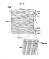
ウェハ表面の電界により引き戻された電子ビームの密度を計算したのが、図4である。図中「構造」欄に示すように3×3に並んだ部分が導電物であり、中央の電位のみを周囲から1V異なる電位とした。下図は、この場合に電子ビームのエネルギー幅(ΔE)を2eVとして電子ビームの軌道計算を実施し、ウェハ表面から戻ってきた電子をプロットしたものである。点の密度が高いところが、電子密度が高いところを示す。中央部に電子が集中し、電子密度が高い部分が存在することが示されており、図2で説明した原理により70nm微細パターンの1Vの変化を検出でき、すなわち導通不良欠陥が検出できることを示している。
【0035】
ここでは、ポイントビームを走査する方式や二次電子を結像する方式と比較して、本発明により検査速度がけた違いに向上することを説明する。電子ビームを用いた画像形成装置の場合、画像取得の速度を制限するものは最終的に画像に必要とされるS/N比に帰着する。画像のS/N比はすなわち画像を形成するのに使われる電子の数で決定される。また必要とされるS/N比は、検出すべき欠陥が画像に生じさせるコントラストの大きさで決まる。すなわち、欠陥コントラストを信号Cとすればそれよりもノイズが小さい必要がある。ノイズNは信号の3σ値で定義される。σ値は照射電子数のショットノイズで決まり、1画素(pixel)当たりに照射される電子数Sの平方根 (√S)となる。従って、ノイズNは3√Sとなる。
【0036】
従来のように電子ビームをウェハ7に衝突させてそのとき発生する二次電子を検出する場合には、さらに試料からの二次電子放出(secondary electron emission) という確率過程が存在するために、二次電子放出をポアソン過程であると仮定すれば、ノイズNはN=(3√2)√Sとなる。そして、たとえば、欠陥コントラストCが平均信号量Sの5%であるとすればC=0.05×Sとなり、ノイズNはN≦0.05×Sである必要があるため、S≧7200となる。この考え方に基づき1cm2あたりの検査時間Tを求めると、以下のようになる。
T=(0.01/x)2・t
=(1.6e−19・0.012・(3√2)2)/(I・η・C2・Pix2) ・・・(1)
なお、t=((1.6e−19・(3√2)2)/(I・η・C2))・(x2/Pix2)
ここで、tはノイズをコントラストCよりも小さくするために電子ビームが同一場所にとどまっていなければならない時間である。つまりSEM式の場合は電子ビームプローブが一画素を照射する時間である。また、面ビーム照射の場合はある一点にビームが向けられている必要がある時間でありこの時間をショット時間と呼ぶことにする。
【0037】
Pixは必要な解像度、xは面積ビーム一辺の長さ(SEM式の場合は画素サイズすなわちPixと同一)、Iはビーム電流、ηは画像形成に使用できる電子の効率である。一方、本発明においては電子ビームはウェハ7の表面に衝突することはなく電界により散乱されるだけなので二次電子放出に伴う確率過程は存在しない。したがって(1)式の√2が不要となり(2)式のようになる。
T=(0.01/x)2・t
=(1.6e−19・0.012・(3)2)/(I・η・C2・Pix2) ・・・(2)
なお、t=((1.6e−19・(3)2)/(I・η・C2))・(x2/Pix2)
ここで、各方式におけるη、Cを見積もることにする。SEM式の場合は照射した電子ビームとほぼ同数の二次電子が放出し、そのほぼ100%を検出器に取り込むことができるためηはほぼ1である。
【0038】
一方、面状の電子ビームをウェハ7に照射し、発生した二次電子を結像する二次電子プロジェクション方式においては、放出する二次電子のうちのごく限られた垂直方向成分の二次電子のみで結像しないと分解能が劣化してしまう。これを図5、図6により説明する。
【0039】
図5は,結像に寄与する二次電子または反射電子の放出半角βに対する画像の分解能を求めたものである。すなわち、結像系に取り込む電子の半開角である。たとえば、放出角100mrad以下の二次電子により画像を形成した場合の分解能は約100nmであることを示している。計算条件として、ウェハに照射する電子のエネルギーは500eV、ウェハ表面は5kV/mmの強電界下にあり、二次電子のエネルギー幅は5eVである。二次電子のエネルギー分布は10eV以上に広がって分布しているが、放出エネルギー2eVを中心とした±2.5eVの成分のみを結像に利用することとした。これは全二次電子のおよそ1/2に相当する。
【0040】
また、反射電子は弾性散乱電子のみを考慮することとして、エネルギー幅は1eVとした。これらの図から、二次電子において例えば分解能を40nmとするためには放出角25mradとする必要があり、この場合放出角β内に二次電子が散乱される確率は約0.1%である。二次電子の放出効率(yield)(照射電子数に対する二次電子数の割合)はおよそ1とすると、二次電子結像型の場合のηは1/2×0.001×1=0.0005となる。
【0041】
一方、反射電子の場合に分解能を40nmとするためには、試料放出角(β)80mradで、その角度内に反射電子の存在する確率は、図6から0.2%である。反射電子の放出効率(照射電子数に対する反射電子数の割合)は、参考文献「Image Formation in Low−Voltage Scanning Electron microscopy、SPIE、Bellingham、p.43、p67、1993」によると、照射エネルギー500eVにおいて0.02〜0.03程度である。したがって、反射電子結像型におけるηは、0.002×0.025=5e−5とかなり小さい値となる。
【0042】
一方、本発明においては、平坦なウェハ面において電子ビームがそのまま垂直上方に跳ね返されるためビームの開き角は照射ビームの角度ばらつきと同等で非常に小さい(数mrad)。図7は、これまでの説明をさらに理解するための説明図である。
【0043】
図7中の左図に示すように、二次電子は試料から180度の広がりをもって真空中に放出されるのに対し、本発明においては、右図に示すようにすべての電子がほぼ真上に上ってくるため照射電子を有効に画像として利用することができる。一方、表面に凹凸や電位分布(potential distribution)が存在する場合は垂直方向でなく、ある角度を持って上方に進むことになる。その場合は結像に直接寄与する電子の割合は減少するが、この角度の変化自体がウェハ表面の画像を形成する要因であるためコントラストが高くなる。すなわち、欠陥のコントラストCが大きくなることと等価で、欠陥検出には有利となる。
【0044】
結局、本発明においては、ηとCは連動しており、ηを制限すればその分Cが増大することになる。厳密にはパターンの種類欠陥の種類によって異なるが、ここでは欠陥部において画像として検出できる信号は全電子の1/2とする。残りの1/2の信号はコントラストに寄与する分である。したがってη=0.5、C=0.5とする。
【0045】
以上をまとめると、表1のようになる。
【0046】
【表1】

【0047】
次に、本発明の一実施例の構成について詳しく説明する。図9に、本発明の一実施例になる検査装置の構成を示す。本実施例による検査装置は、大別して、電子光学系101、試料室102、画像検出部103、画像処理部104および制御部105より構成されている。それぞれの部分について以下に説明する。
【0048】
まず、電子光学系101について説明する。加速電源23により負の高電位が与えられている電子源1から放出された加速電子ビームは、コンデンサレンズ2によって収束され、矩形の開口を有する絞り4を照射する。電子源1には、Zr/O/W型のショットキー電子源を用いた。大電流ビーム(例えば、1.5μA)で、かつエネルギー幅が1.5eVの均一な面状電子ビームを安定に形成できる。そして、ビームセパレータ3によってウェハ7の方向に偏向される。ビームセパレータ3は、電子源1からの入射電子ビームと試料からのミラー電子ビームの光路を分離するためのものである。コンデンサレンズ2は、クロスオーバを対物レンズ6の焦点面に形成する。また、対物レンズ6によってウェハ7表面上に絞り4の像を形成するように絞りやレンズの配置を最適化してある。
【0049】
これにより、ウェハ7表面に垂直な方向を向き、各電子同士の軌道がほぼ平行に揃ったビームで、かつ絞り4の開口形状に整形された面状の電子ビームが形成される。絞り4上での矩形絞り開口の大きさは、例えば100μm角であり、対物レンズ6によってこれを1/2に縮小し、ウェハ7表面上では50μm角の面状電子ビームが得られるようにした。この面状電子ビームは、照射系偏向器5によってウェハ7表面上の任意の位置に移動(または、走査)され得る。
【0050】
対物レンズの前焦点面とクロスオーバ位置を完全に一致できなくてもある許容範囲内であれば問題ない。また、クロスオーバの大きさも理想的にはゼロであるが、実際は電子銃やコンデンサレンズの収差により有限の大きさを持っている。この大きさもある許容範囲であれば問題ない。このクロスオーバの位置を正確に制御し、しかも電子銃やコンデンサレンズの収差を十分に低減させた電子光学系では、試料への入射角の広がりは0.5mrad以下に抑えることができた。この入射角の広がりはミラー電子による試料表面の拡大像の分解能を決める要因のひとつであり以下の式で表される。
【0051】
r0=β2・Zm …(3)
ここで、r0は入射角の広がりで決まる分解能、βは最大入射半角、Zmは電子を引き戻す電界が生じている距離である。
【0052】
本実施例では、βは0.25mrad、Zmは5mmである。これを(3)式に代入すると、r0は0.3nmとなり、本実施例では分解能に影響を与えないことがわかる。したがって、ビーム電流は必要に応じてもっと増やすことが可能である。
【0053】
なお、分解能が30nm程度でも半導体の欠陥検出には十分であると考えられるので、Zmが5mmとすれば、βは2.4mradまで許容できることになる。この場合は、対物レンズの前焦点面とクロスオーバの位置のずれやクロスオーバの大きさにはかなり余裕が生じる。
【0054】
前焦点面でのビーム開き半角をαとし、対物レンズの焦点距離をf、クロスオーバの位置ずれをΔf、面状電子ビームの半径をXとすれば、次の式が成り立つ。
【0055】
Δf=f・β/α ・・・(4)
α=X/(2f) ・・・(5)
式(4)(5)から、例えば対物レンズの焦点距離fが10mmで面状ビームの大きさXを40μmとしたときは、クロスオーバ位置のずれΔfが10mm程度ずれても問題ない。これを前焦点面でのビーム直径に換算すると約40μmとなる。いずれにしろ、電子ビームのクロスオーバを対物レンズの前焦点面の近傍に配置させることで十分な分解能を得られることがわかる。
【0056】
ここで、ビームセパレータ3について簡単に説明する。ビームセパレータ3は、電子源1から放出された電子ビームをウェハ7の方向に電子ビームを偏向し、一方、ウェハ7から引き戻されたミラー電子は電子源1の方向ではなく結像レンズ11の方向に偏向する。このような作用の偏向器には磁場による偏向器が最適である。磁場による偏向作用は電子の入射方向によって偏向作用の方向が異なるからである。
【0057】
また、実施例2として図10を用いて後述するが、結像レンズの光軸と対物レンズ6の光軸を一直線上に配置した光学系の場合は電場と磁場を直行させて、下からのミラー電子は直進させ、上からの電子ビームのみに偏向作用を持たせるE×B偏向器を用いる。
【0058】
ウェハ7、ウェハ(試料)移動ステージ8には、電源9により、電子源1よりも僅かに高い(絶対値の大きい)負電位を印加する。具体的には0.5〜5Vだけ負電位にするのが良い。あまり高い負電位にすると画像の分解能が劣化する。また、あまり小さい電位では表面の凹凸や電位等のわずかな変化を極端に強いコントラストとして画像化してしまい、真に必要な欠陥のみを検出することが困難となってしまう。
【0059】
ウェハ7表面に垂直に向けられた電子ビームは、上記の負電位によってウェハ7の手前で減速されてウェハ7表面の電界によって上方に引き戻される。この電子はウェハ7の表面の情報を反映していることは既に説明した。このミラー電子は、対物レンズ6により焦点を結び、ビームセパレータにより結像系偏向器10および結像レンズ11の方向に偏向される。そして結像レンズ11によりウェハ7表面の状態を電子像として結像させる。この電子像を拡大レンズ13、14によって蛍光板15上に拡大投影させることによって、ウェハ7表面のパターンや帯電状態を反映した蛍光像(顕微鏡像)を得ることができる。
【0060】
この電子像のコントラストと分解能を向上するために、クロスオーバ面にコントラストアパーチャ12を挿入できるようになっている。このコントラストアパーチャ12によって、ウェハ7表面電場で引き戻されたときに垂直方向から大きく外れた電子を取り除くことにより画像の分解能とコントラストが強調できる。
【0061】
本発明の画像形成原理において、ウェハ表面の帯電の微妙な違いを検出するための感度や画像の分解能は面状電子ビームのエネルギー幅によって決まってくる。これをシミュレーションにより比較した結果が、図10である。図4と同様のパターンを仮定し、電子ビームのエネルギー幅(ΔE)を2eVと4eVの二通りの場合について得られる画像を比較した。
【0062】
この結果によると、4eVのエネルギー幅を仮定した場合、パターン中央部の電位の異なる部分のコントラストが認められない。半導体の微細化の進展を考慮したとき、図10に示したような微細パターンにおいて1V程度の帯電電位の違いを欠陥として検出することが必要となってくる。したがって、本発明において用いる電子ビームのエネルギー幅は2eV以下であることが望ましいことがわかる。
【0063】
前述のように、Zr/O/Wショットキー電子源を用いた本実施例においては、エネルギー幅が1.5eVであるので問題ない。たとえば、もっとエネルギー幅の大きい電子源を用いた場合には、電子ビームの光路上にエネルギーフィルタを設け、電子源から電子が放出されてから最終的に画像が形成されるまでの間に電子のエネルギー幅を2eV以下にする必要がある。エネルギーフィルタは電子源からウェハ7の間に設けることが望ましいが、ウェハ7からのミラー電子に対してエネルギーフィルタリングを実施しても同様の効果は得られる。
【0064】
本発明では、電子ビームがウェハ7に衝突することがない。したがって、原則的にはウェハ7表面に絶縁膜が存在していても表面が帯電することはない。したがって、帯電させない状態で検査を実施すれば、検出できる欠陥は形状欠陥(形状が正常部と異なっているもの)のみである。
【0065】
しかし、電子ビームを用いた半導体パターンの欠陥検査において、導通不良や、絶縁されるべきものがショートしている、またはリーク電流が正常部と比べて大きいというような、いわゆる電気的欠陥と呼ばれているものを電子ビームの照射によって帯電させ、その電位の違いによって発生するSEM画像の電位コントラストにより検出する方法が行われている。
【0066】
このような欠陥を高感度に検出できるように、本発明では検査画像を取得する前にあらかじめ帯電制御専用の電子ビームを照射する予備帯電制御装置を備えている。この装置によりウェハ7をあらかじめ所定の電位に帯電させてから検査を実施すれば、形状欠陥だけでなく導通不良部のような電気的欠陥を検出できる。以下、この動作と構成について説明する。
【0067】
図11は、予備帯電制御装置の動作原理を説明する図である。電子源41は、大電流の電子ビームをある程度の広さ(数百μm〜数十mm)を持った面から放出する電子源である。たとえば、カーボンナノチューブを束ねた電子源やタングステンフィラメント熱電子源、あるいはLaB6電子源等を用いることが可能である。引出グリッド42に引出電極48により引出電圧を印加して電子源41から電子ビーム43を放出させる。電子ビームは、制御グリッド44を通過して絶縁膜46に照射される。これにより二次電子45が放出する。
【0068】
この二次電子は、絶縁膜46の表面の電位を基準としておよそ2eVのエネルギーを持っている。絶縁膜表面が基板47の電位と同等であれば電子ビームの照射エネルギーは加速電源49の電圧であり、この電圧は二次電子放出効率が1以上となるような値に設定しておく。一般的な半導体デバイス用の絶縁膜材料では500Vで良い。このとき、二次電子放出効率が1より大きいため、絶縁膜表面は正に帯電していく。
【0069】
制御グリッド44には制御電源50が接続されており任意の正または負の電圧を印加できるようになっているので、絶縁膜表面の電位が制御グリッド44の設定電位よりも正になり、二次電子が絶縁膜表面に引き戻されるようになると絶縁膜表面の正への帯電が止まる。このとき、絶縁膜表面の帯電電位は制御グリッドの電位よりやや低い(約2V)正の電位で安定することになる。制御グリッドの電位と等しくならないのは、二次電子がエネルギーを持っているためである。以上のような原理によって、絶縁膜46表面の電位を制御グリッド44の電位によって制御することが可能となる。
【0070】
図12は、カーボンナノチューブ電子源を用いた予備帯電制御装置の構成である。電子源41は、碍子51により真空内に保たれた状態で保持され、電位を印加できるようになっている。制御グリッド44はウェハ7に面して配置され、引出グリッド42が電子源51から電子を引き出す。
【0071】
図13は、LaB6電子源を利用した予備帯電制御装置の構成である。LaB6電子源を顕微鏡に用いる場合は、ウェーネルト電極を用いて電子放出直後にクロスオーバを形成させるが、この場合は光源が小さい必要がないので代わりに引出電極42’を設けている。
【0072】
試料室102内では、2次元(X、Y)方向に移動可能な試料移動ステージ8上にウェハ7が載置され、ウェハ7には電源9により前述のように電子ビームの大部分がウェハ7に衝突しないような負電位が印加されている。試料移動ステージ8にはステージ位置測定器27が付設され、ステージ位置をリアルタイムで正確に計測している。これは、ステージ8を連続移動させながら画像を取得するためである。このステージ位置測定器27には、例えばレーザ干渉計(laser interferometer)が用いられる。
【0073】
また、半導体試料(ウェハ)表面の高さを正確に計測するために、光学的な試料高さ測定器26も取りつけられている。これには、例えば、ウェハ表面上の検査すべき領域に斜め方向から光を入射させ、その反射光の位置変化からウェハ表面の高さを計測する方式のものを用いることができる。この他、試料室102には、検査領域の位置決め用に用いられる光学顕微鏡31も付設されている。
【0074】
次に、試料移動ステージ8の整定時間について述べる。ステージ8の移動方法をステッフ゜・アンド・リピート方式とすると、ステージ8の整定時間は、msecオーダが必要となるため、画像S/N比を向上させて画像取得時間を短縮してもステージ移動に時間がかかってしまい検査時間を短縮することができない。従って、ステージ8の移動方法は、ステージが常にほぼ等速で移動している連続移動方式とした。これによりステージの整定時間による検査時間の制約はなくなる。ただし、ステージ8が連続移動していると、同一場所の画像を形成するのに必要な時間である1ショットの間にもステージ8が移動して、試料表面上での照射位置が変化してしまう。そこで、1ショットの間に照射位置が変化しないように、照射系偏向器5により照射電子ビームをステージ8の移動に追従させるようにした。また、静止座標系である電子光学系から見ると、電子ビーム照射位置は移動するから結像レンズ11により作られる像12も移動してしまう。この移動が生じないようにするために、結像系偏向器10を照射系偏向器5と連動動作させるようにした。
【0075】
次に、画像検出部103について説明する。画像検出には、ミラー電子の像12の拡大像を光学像に変換するための蛍光板15と光学画像検出素子(例えばCCD素子)17とを光ファイバー束16により光学結合させる。これにより蛍光板15上の光学像を光学画像検出素子17の受光面上に結像させる。光ファイバー束16は、細い光ファイバーを画素数と同じ本数束ねたものである。また、上記光ファイバー束16の代わりに光学レンズを用い、光学レンズによって蛍光板15上の光学像を光学画像検出素子(CCD)17の受光面上に結像させるようにしてもよい。蛍光板15の両面には電極300と透明電極301を設け、両電極間に透明電極301側が正の高電圧を印加して電子ビームの散乱を防いでいる。光学画像検出素子(CCD)17は、その受光面上に結像された光学像を電気的な画像信号に変換して出力する。出力された画像信号は、画像処理部104に送られ、そこで画像信号処理が行われる。
【0076】
次に、画像検出素子(CCD)の読み取り時間について述べる。本実施例では、CCD17に蓄積された電荷を128チャンネルの読み出し口から8Mライン/秒の読出速度で多チャンネル並列読み出しできるようにした。1チャンネル1ライン当たりの画素数は8で、1ライン当たりの読み出所要時間は125nsecである。従って、1画素当たりの読み出所要時間は125nsec/8(画素)=16nsecとなる。これに対し、CCDからの画像データの読み出しが1チャンネル方式では、非常に高速での読み出しが必要となり、実現困難である。
【0077】
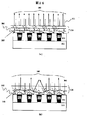
本実施例では、CCDからの画像データの読み出し口を128チャンネルに分け、この128チャンネルで並列同時読み出しする方式とすることによって、1画素当たりの読み出し所要時間を16nsecとし、十分実現可能な読出速度としている。これを模式的に示したのが、図14である。
【0078】
CCD17からの画像データの読出チャンネル数は128chであり、各チャンネル毎に8画素×1024ラインがあるから、このCCDから一枚の画像データを読み出すに必要な時間は約125μsecとなる。すなわち、1ショット領域の画像信号を125μsecで取り込めることになり、画素サイズ50nm、1ショット領域を50μm角とすれば試料表面積1cm2当たりの検査所要時間は5secとなる。
【0079】
以上のように、画素サイズ50nmで検査した場合の従来方式による試料面積1cm2当たりの検査所要時間約400secに比べて、80倍もの高速化が達成できた。また、本実施例では、検査所要時間を決めているのはCCD素子からの信号読み出し速度であるので、将来CCD素子におけるより高速のデータ読み出し方式が実現されれば、さらなる検査の高速化が期待できる。
【0080】
画像処理部104は、画像信号記憶部18及び19、演算部20、欠陥判定部21より構成されている。画像記憶部18と19は同一パターンの隣接部の画像を記憶するようになっており、両者の画像を演算部20で演算して両画像の異なる場所を検出する。この結果を欠陥判定部21により欠陥として判定しその座標を記憶する。なお、取り込まれた画像信号はモニタ22により画像表示される。
【0081】
装置各部の動作命令および動作条件は、制御部105内の制御計算機29から入出力される。制御計算機29には、予め電子ビーム発生時の加速電圧、電子ビーム偏向幅・偏向速度、試料ステージ移動速度、画像検出素子からの画像信号取り込みタイミング等々の諸条件が入力されている。ビーム制御系28は、制御計算機29からの指令を受けて、ステージ位置測定器27、試料高さ測定器26からの信号を基にして補正信号を生成し、電子ビームが常に正しい位置に照射されるように対物レンズ電源25や走査信号発生器24に補正信号を送る。ステージ制御系30は、制御計算機29から指令を受けて試料移動ステージ8を制御する。
【0082】
次に、実際の検査手順について説明する。まず、光学顕微鏡31と電子ビーム画像を用いてのアライメントの方法について説明する。ウェハ7をウェハ移動ステージ(X−Y−θステージ)8上に載置し、光学顕微鏡31の下へ移動する。モニタ22によりウェハ7表面の光学顕微鏡画像を観察し、画面内の例えば中央に現れた任意のパターンを記憶する。この際、選択するパターンは電子ビーム画像上でも観察可能なパターンである必要がある。
【0083】
次に、上記の光学顕微鏡画像を用いてウェハ7表面上の回路パターンがステージ移動方向と平行あるいは直交となるように、ウェハ移動ステージ8により回転補正を行う。回転補正時には、あるステージ位置におけるウェハ7表面上の回路パターンの任意のチップ内の任意のパターン部分の光学画像を取り込んでモニタ22に表示させて、表示画面内の任意箇所にマーキングを付す。そして、その光学画像信号を記憶部18に記憶させる。
【0084】
次に、ウェハ7表面上の回路パターンの数チップ分の距離だけステージ8をx方向またはy方向に移動させ、新たなチップ内の先と同一のパターン部分の光学画像を取り込んでモニタ22に表示させる。そして先のマーキング箇所に対応する箇所にやはりマーキングを付した後、その新たな光学画像信号を記憶部19に記憶させる。次いで、演算部20において、記憶部18、19に記憶された光学画像信号同士を比較演算して、両画像間でのマーキング箇所の位置ずれ量を算出する。このマーキング箇所の位置ずれ量と両画像間でのステージ移動量とから、ウェハ7の回転角度誤差を算出し、その分ステージ8を回転させて回転角度を補正する。以上の回転補正操作を数回繰り返して、回転角度誤差が所定値以下となるようにする。
【0085】
さらに、光学顕微鏡画像を用いてウェハ7表面上の回路パターンを観察し、ウェハ上でのチップの位置やチップ間の距離(例えば、メモリセルのような繰り返しパターンの繰り返しピッチ)を予め測定し、その値を制御計算機29に入力する。そして、ウェハ7表面上の被検査チップおよびそのチップ内の被検査領域をモニタ22の光学顕微鏡画像上で設定する。光学顕微鏡画像は、比較的低倍率で観察が可能であり、また、ウェハ7表面の回路パターンが例えばシリコン酸化膜のような透明な膜で覆われている場合でもその下地まで観察可能である。したがって、チップ内回路パターンのレイアウト等が簡便に観察でき、検査領域の設定が簡便に行える。
【0086】
次に、ウェハ7を電子光学系の下へ移動する。そこで、先に光学顕微鏡画像上で設定した被検査領域を含むと予想される領域の電子ビーム画像を取得する。この時、1ショット領域内に上記の被検査領域が入るようにする。この電子ビーム画像上においても、先の光学顕微鏡画像上においてマーキングしたのと同じ画面内に、先にマーキングした箇所のパターンが現れるようにステージ8を移動する。これにより、予め検査開始前に電子ビーム照射位置と光学顕微鏡観察位置との間の対応をつけ、かつ、画像取得位置を校正することができるようになる。そして、この電子ビーム画像上において、先に光学顕微鏡像上で行ったのと同様の操作を実施する。これにより、光学顕微鏡を用いての簡便な観察位置の確認や位置合わせ、および電子ビーム照射位置の調整が可能となる。
【0087】
さらには、ある程度の回転補正も実施した後に、光学顕微鏡画像に比べて分解能が高く、高倍率画像を得ることのできる電子ビーム画像を用いてさらに高精度な回転補正ができるようになる。さらに、この電子ビーム画像を用いて、被検査領域または同一パターン領域を高倍率で高精度に観察確認・補正することができる。ただし、半導体ウェハ7の表面の全部(または一部)が絶縁物で覆われている場合には、絶縁物表面の帯電電位が基板電位と等しくなっていない可能性があるので画像取得前に呼び帯電制御装置32によって表面の帯電電圧を制御しておく必要がある。
【0088】
上記した検査条件の設定が完了したら、半導体ウェハ7表面上の被検査領域の一部を実際の検査条件と全く同一の条件で電子ビーム画像化し、被検査領域の材質や形状に依存した画像の明るさの情報およびそのばらつき範囲を算出しテーブルにして記憶する。そして、後の検査工程において該記憶テーブルを参照して実際に画像化検出された被検査領域内のパターン部分が欠陥であるか否かを判定する際の判定条件を決定する。
【0089】
上記の手順によって被検査領域および欠陥判定条件の設定が完了したら、実際に検査を開始する。検査時には、試料(半導体ウェハ)7を搭載したステージ8はx方向に一定速度で連続移動する。その間、電子ビームは各1ショットの間ウェハ7表面上の同一照射領域(面積領域)を一定のショット時間(本実施例では、50μsec以上)照射する。ステージ8は連続移動しているので、電子ビームは照射系偏向器5によってステージ8の移動に追従して偏向走査させる。
【0090】
電子ビームの照射領域あるいは照射位置は、ステージ8に設けられたステージ位置測定器27、試料高さ測定器26等により常時モニタされる。これらのモニタ情報が制御計算機29に転送されて詳細に位置ずれ量が把握され、かつこの位置ずれ量はビーム制御系28によって正確に補正される。これにより、パターンの比較検査に必要な正確な位置合わせが高速・高精度で行われ得る。
【0091】
また、半導体ウェハ7の表面高さを、電子ビーム以外の手段でリアルタイムに測定し、電子ビームを照射するための対物レンズ6や結像レンズ11の焦点距離をダイナミックに補正する。電子ビーム以外の手段としては例えば、レーザ干渉方式や反射光の位置変化を計測する方式等による光学式の高さ測定器26である。これにより、常に被検査領域の表面に焦点のあった電子ビーム像を形成することができる。また、予め検査前にウェハ7の反りを測定しておき、その測定データを基に上記の焦点距離補正をするようにして、実検査時にはウエハ7の表面高さ測定を行う必要がないようにしてもよい。
【0092】
電子ビームをウェハ7表面に向け、ミラー電子によりウェハ7表面上の所望の被検査領域(面積領域)についての拡大光学像を蛍光板15上に形成する。この拡大光学像をCCD素子17により電気的な画像信号に変換し、この画像信号を画像処理部104に取り込む。そして、制御計算機29からの指令を受けて制御部28により与えられた電子ビーム照射位置に対応した面積領域についての電子ビーム画像信号として、記憶部18(または19)に格納する。
【0093】
半導体ウェハ7表面上に形成された同一設計パターンを有する隣接チップA、B間でのパターンの比較検査をする場合には、先ず、チップA内の被検査領域についての電子ビーム画像信号を取り込んで、記憶部18内に記憶させる。次に、隣接するチップB内の上記と対応する被検査領域についての画像信号を取り込んで、記憶部19内に記憶させながら、それと同時に、記憶部18内の記憶画像信号と比較する。さらに、次のチップC内の対応する被検査領域についての画像信号を取得し、それを記憶部18に上書き記憶させながら、それと同時に、記憶部19内のチップB内の被検査領域についての記憶画像信号と比較する。このような動作を繰り返して、全ての被検査チップ内の互いに対応する被検査領域についての画像信号を順次記憶させながら、比較して行く。
【0094】
上記の方法以外に、予め、標準となる良品(欠陥のない)試料についての所望の検査領域の電子ビーム画像信号を記憶部18内に記憶させておく方法を採ることも可能である。その場合には、予め制御計算機29に上記良品試料についての検査領域および検査条件を入力しておき、これらの入力データに基づき上記良品試料についての検査を実行し、所望の検査領域についての取得画像信号を記憶部18内に記憶する。次に、検査対象となるウェハ7をステージ8上にロードして、先と同様の手順で検査を実行する。
【0095】
そして、上記と対応する検査領域についての取得画像信号を記憶部19内に取り込むと同時に、この検査対象試料についての画像信号と先に記憶部18内に記憶された上記良品試料についての画像信号とを比較する。これにより上記検査対象試料の上記所望の検査領域についてのパターン欠陥の有無を検出する。なお、上記標準(良品)試料としては、上記検査対象試料とは別の予めパターン欠陥が無いことが判っているウェハを用いても良いし、上記検査対象試料表面の予めパターン欠陥が無いことが判っている領域(チップ)を用いても良い。例えば、半導体試料(ウェハ)表面にパターンを形成する際、ウェハ全面にわたり下層パターンと上層パターン間での合わせずれ不良が発生することがある。このような場合には、比較対象が同一ウェハ内あるいは同一チップ内のパターン同士であると、上記のようなウェハ全面にわたり発生した不良(欠陥)は見落とされてしまう。
【0096】
しかし、本実施例によれば、予め良品(無欠陥)であることが判っている領域の画像信号を記憶しておき、この記憶画像信号と検査対象領域の画像信号とを比較するので、上記したようなウェハ全面にわたり発生した不良をも精度良く検出することができる。
【0097】
記憶部18、19内に記憶された両画像信号は、それぞれ演算部20内に取り込まれ、そこで、既に求めてある欠陥判定条件に基づき、各種統計量(具体的には、画像濃度の平均値、分散等の統計量)、周辺の画素間での差分値等が算出される。これらの処理を施された両画像信号は、欠陥判定部21内に転送されて、そこで比較されて両画像信号間での差信号が抽出される。これらの差信号と、既に求めて記憶してある欠陥判定条件とを比較して欠陥判定がなされ、欠陥と判定されたパターン領域の画像信号とそれ以外の領域の画像信号とが分別される。
【0098】
これまでに述べてきた検査方法および検査装置により、ウェハ7の表面の電位および形状の情報を反映した画像を形成し、対応するパターン領域についての画像信号を比較検査することによって、パターン欠陥の有無を検出することが可能となった。これにより、従来の電子ビームによる検査装置と比べ非常に高速な検査が可能になった。
【0099】
(実施例2)
実施例1では、1ショットの電子ビーム照射領域の面積が50μm×50μmとかなり大きいため、半導体試料の拡大像の周辺部に歪みが生じると云う問題や照射領域内でのビーム電流密度の均一性に問題が生じる場合がある。画像歪みや電流密度の不均一性が固定的に生じている場合には、光ファイバー束16のファイバー素線配列に変化を付けることで補正可能である。また、画像信号の取得感度や画像処理に重みを付けることでも補正できるが、それらが時間的に変動する場合には、それらの方法では対応が困難となる。
【0100】
本実施例では、1ショットの照射領域を5μm角として、1ショットの照射領域内では歪みや電流密度の不均一性の問題が生じないようにした。照射電子ビーム電流は1ショット当たり1μAである。この時、電子ビームの照射時間は電子の結像効率ηを0.5とすると、先の(1)式より、1ショット当たりの照射時間tは、0.18μsecとなる。ショット時間0.18μsecで一つの照射領域(5μm角)を照射した後、電子ビームは照射系偏向器5により隣接する次の照射領域(5μm角)上に移動される。このようにして、次々に照射位置を移動して、x方向100μm×y方向100μmの範囲全体を20×20=400ショットで照射する。
【0101】
この時、CCD素子17上には、各1ショット毎に、その時の電子ビーム照射位置に対応した位置に拡大像が得られ、電子ビームの走査による電子ビーム照射位置の移動に応じてCCD素子に得られる拡大像位置も移動して行く。この様子を示したのが、図15である。
【0102】
CCD素子17には1024×1024画素のものを用いた。CCD素子上での1画素はウェハ7表面上での50nm角の領域に相当し、従って、ウェハ7表面上での1ショットの照射領域(5μm角)は、CCD素子受光面上での100×100画素の領域(CCD素子受光面全体の1/100に相当する)となる。そして、CCD素子の受光面全体で試料表面上の50μm角の領域をカバーできるようにした。従って、試料表面上での50μm角の領域の拡大像を得るためには、0.18(μsec)×100(ショット)=18(μsec)を要することとなる。
【0103】
上述のようにして、ウェハ7表面上の50μm角の領域の画像を18μsecでCCD上に形成させたら、CCDに蓄積された画像信号をデジタル信号として画像記憶部18に記憶させる。試料表面上の隣接する次の領域の画像信号を取得するためにはステージ8を50μm移動させる必要がある。このステージ移動には、先の実施例1の場合と同様、ステージ8を一定速度で連続移動(continuous moving)させる方式を採った。その際、照射電子ビームに対してステージ8があたかも静止しているかの状態になる様、照射系偏向器5によって照射電子ビームをステージ8の移動に追従させて偏向走査するようにした。これにより、ステージ8を移動・停止させる際に生じる無駄時間をゼロにした。
【0104】
この連続移動ステージ8への照射電子ビームを追従させながら走査するためには、ビーム制御系28内で、ステージ位置測定器27からの信号を参照して偏向信号の補正信号を計算し、この偏向補正信号を照射系の偏向器5に送り照射電子ビームの偏向を制御させる。さらに、電子ビームによる試料拡大像の歪みや位置ドリフト等に関する補正分も上記の偏向信号の補正信号に重畳させることにより、これらの補正も行うようにした。また、照射系偏向器5と連動して結像系偏向器10も動作させて、CCD上での試料拡大像の位置が上記のステージ追従によるビーム位置移動の影響を受けないようにした。これにより、ステージ移動による無駄時間を無くし、高速・高精度の検査を実現することができた。なお、上記以後の欠陥検査のための画像処理等については、先の実施例1の場合と同様である。
【0105】
以上説明した手順により検査を進めていくと、試料表面1cm2当たりについての拡大像をCCD上に順次形成するに要する時間Tは0.72secとなる。一方、先の実施例1の場合と同様に、CCDから一枚の画像(試料表面50μm角についての画像)を読み出すのに125μsecが必要であるため、試料表面積1cm2当たり5secが必要となる。CCD素子における画像形成と画像信号の読み出しは並行して行われるから、検査に要する時間は、画像形成に要する時間と画像信号読み出しに要する時間との内何れか長い方の時間となる。本実施例では、画像形成所要時間より画像信号読み出し所要時間が長く、1cm2当たり5secとなっており、従って、本実施例における試料表面積1cm2当たりについての検査所要時間は5secとなる。
【0106】
以上の説明では、1ショットの電子ビーム照射領域を5μm角の大きさに固定した場合について例示したが、半導体ウェハ7表面でのパターン繰り返しピッチに応じて、この電子ビーム照射領域の大きさを可変できるようにしても良い。上述したように、本実施例では、1ショットの電子ビーム照射領域をより小さく設定している。したがって、各照射領域間のつなぎ部分に多少の歪みが生じたとしても、常に同一箇所に同程度の歪みが生じることになり、相互比較すべき二つの画像上での歪みの現れ方も等しくなるため、歪みによる誤検出の問題が無くなる。これにより、信頼性の高いパターン欠陥検査が実現できる。
【0107】
(実施例3)
本実施例では、試料表面画像を電気信号に変換する素子として、時間蓄積型のCCDセンサを用いた。この素子はTDIセンサと呼ばれるもので、光学式検査装置において一般的に使用されている。それ以外は、先の実施例2の場合と同様である。このTDIセンサの動作概念を、図16を参照して説明する。
【0108】
TDIセンサでは、各受光領域で受光した光の強度に応じて生成された電荷をx方向のラインに移動させて行くと同時に、その移動先で受光した光の強度に応じて生成された電荷を順次足し合わせて行くように動作する。そして、受光面の最終ラインに達した時点で電気信号として外部に出力する。従って、x方向の電荷の移動速度と受光面上の画像のx方向の移動速度を同一にすることで、画像がセンサ上を移動する間の信号を積分して出力することになる。
【0109】
本実施例では、先の実施例1から実施例4の場合のCCDセンサと同様に、信号読み出しを128チャンネルに分割しそれぞれ並行して読み出すことにより、読出速度を4Mライン/秒とした。また、受光領域の大きさは、x方向に64画素、y方向に2048画素のものを用いた。1ラインのx方向長さは、試料表面上の50nm、y方向長さは約100μmに相当する。このとき、縦50nm、横100μmの画像が4M/秒の速度で出力されることになるため、ステージの連続移動速度もこれと同じ速度(50nm/250nsec=200mm/sec)としている。このように、検査領域のx方向移動はステージ8を移動させることにより行う。
【0110】
一方、1ショットの照射領域は5μm角であるので、図16のように、照射領域のy方向移動は電子ビームを走査して行う必要が生じる。すなわち、ステージ8がx方向に1ショット分(5μm)だけ移動する間に電子ビームをy方向に100μm走査する必要がある。1ショットの所要時間を1.25μsecとすると、y方向に100μm(20ショット分)を走査するには25μsec必要となる。一方、ステージ8のx方向移動速度は200mm/secであるから、ステージ8がx方向に丁度1ショット分(5μm)移動するに要する時間は25μsecとなる。このように、x方向に1ショット分(5μm)のステージ移動に要する時間とy方向に20ショット分(100μm)の電子ビーム走査に要する時間とを一致させ、無駄時間が生じるのを防いでいる。この方法によって試料表面積1cm2の画像を取得するには、上述の5μm×100μmの単位走査領域についての走査所要時間(25μsec)の2×105倍を要することになるので、試料表面積1cm2当たりの検査所要時間は5secとなる。
【0111】
上述したように、本実施例では、TDIセンサの信号出力速度から決まるステージの移動速度が200mm/secであるから、十分ステージ移動による検査領域のx方向移動が可能である。しかもその間に電子ビームの検査領域上y方向走査のための十分な時間を確保できる。また、本実施例では、検査速度を決めているのはTDIセンサの信号出力速度であるため、この信号出力速度が改善されれば、さらに高速での検査が実現できる。
【0112】
(実施例4)
本実施例は、SEM画像が取得可能な電子光学系を採用したものである。図17に、その構成を示す。
【0113】
電子源201、コンデンサレンズ202およびSEM用対物レンズ233は、SEMの電子光学系を構成する要素をそのまま採用している。電子源201は、Zr/O/Wショットキー電子源を採用した。この電子源から引出した電子はビームセパレータ243により偏向を受け、静電セクタ(electrostatic sector electrode)型の電子偏向器205により大角度の変更を受けてビームセパレータ203に導かれ対物レンズ206に垂直入射する。電子ビームは対物レンズの前焦点面でクロスオーバを結んでおり対物レンズ206によりウェハ207の表面に垂直な方向にそろった面状電子ビームとなる。ウェハ207に印加する電圧や絞りの配置等に関しては実施例1と同等である。
【0114】
本実施例では、ウェハ検査後に検出した欠陥の画像を詳細に観察したい場合に装置からウェハ7を取り出さずに高分解能なSEM画像を観察できることが特徴である。すなわち、ビームセパレータ243を動作させずに電子ビームを直進させるようにし、同時にウェハ移動ステージ208によりウェハ207をSEM用対物レンズ233の光軸下に移動すればウェハ207の任意の位置の観察が実行できる。なお、図中、211は結像レンズ、213、214は拡大レンズ、222はSEM用コンデンサレンズ、228はビーム制御系、232は予備帯電制御装置、252は試料室、263は画像検出部を示す。
【0115】
この機能は、検出した欠陥の観察だけでなく検査前のウェハのパターン確認や検査条件設定、アライメント等でも活用できる。
【0116】
(実施例5)
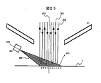
本実施例は、試料に注入して正常パターンと欠陥パターンとの電位差を生じさせる電子線と、試料に当たらずに反射して結像する電子線とをほぼ同じ場所でほぼ同時に照射する手段を設けたものである。図18にその構成を示す。電子源1より放出された電子線は、ビームセパレータ3によりウェハ7に垂直な光軸方向に偏向され、対物レンズ6により試料(ウェハ)表面に垂直な方向にそろった面状の入射電子線301が形成される。 試料(ウェハ)7には、電子線の加速電圧とほぼ同じ負の電位が試料印加電源9によって印加されている。試料印加電源9は円孔レンズ電極41と試料7の間の電位差をも設定できるようになっており、円孔レンズ電極(aperture lens electrode)41と試料7の間の減速電界を可変できるような構成である。たとえば、形状欠陥を検出する場合には、減速電界を通常より強く設定して形状欠陥の検出感度を向上させることができる。円孔レンズ電極41と試料7の間で入射電子線301は急速に減速されて、試料7の表面に形成された半導体パターン形状や帯電の状態を反映した電界により入射電子線301は試料に吸収されるか、試料の直上で向きを変えて反射電子線302となる。
試料7の表面に絶縁物が存在する場合には、入射電子線301を試料7に注入して、絶縁物が帯電した状態で画像を取得する。たとえば、図19の断面図は、シリコン基板(Si)310上に絶縁膜(SiO2膜)311が形成されたウェハにコンタクトホール加工後タングステン(W)の電極部が埋め込まれた試料を示したものである。電極部は基板と低抵抗で導通している正常電極部312と、中央部には電極の底にあるSiO2の残渣(residue)により基板と高抵抗状態である不良電極部313がある。
一次電子線に対する二次電子の放出比(the mean number of secondary electrons excited per incident electron )が1より小さい極低エネルギーの電子線を絶縁物試料に照射すると、絶縁物試料は負電荷(電子)が蓄積することにより負帯電する。例えば、SiO2は約30eV以下の照射エネルギーで、二次電子の放出比が1未満となり負帯電する。図19(a)は絶縁膜311を負帯電させる場合の初期照射の状態を示したものである。試料7に照射する入射電子線301のエネルギーは、試料7が帯電しない初期状態において、照射エネルギーeV0を含むエネルギー拡がり(energy spread)を持ったものとする。ここで、照射エネルギーは試料7に対する電子源1の電位差と照射電子線のエネルギー拡がりで定められるものである。入射電子線301を試料7に照射し続けると、絶縁膜311の負帯電は低エネルギーの入射電子線を反発するようになるまで進行し、絶縁膜311に進入する電子数と絶縁膜311から周辺へ逃げていく電子数が釣り合った電位まで負帯電して安定する。特に、絶縁膜311中に蓄積した電子が周辺部に逃げていかない場合には、絶縁膜311は入射電子線301が進入しなくなる電位まで負帯電して安定する。電極部もまた、進入する電子と電極部から周辺へ逃げていく電子数が釣り合うような電位になる。すなわち、正常電極部312に注入された電子は低抵抗で接触している基板310に流れ込むのでほとんど負帯電しないが、不良電極部313は抵抗値が大きく、周辺部へ逃げていく電子数が小さいので負帯電した状態となる。図19(b)に示すように、等電位面314はこれらの電極および絶縁物電位を反映し、V0の等電位面315が絶縁膜311および不良電極部313の直上近傍に形成されて、エネルギーV0より小さい入射電子線301を反射させるが、正常電極部312の直上近傍にはV0の等電位面315が形成されずに入射電子線301は正常電極部312に衝突するので、反射電子線302の結像像(image)は正常電極部312と不良電極部313の直上近傍の等電位面形状の差を反映した像となる。
図21(a)は3x3列の70nm角プラグパターンの正常部が0V、中央パターンの不良部が−1V、SiO2膜が−2Vに帯電した場合に、正常部電位0Vより1.2Vほど大きなエネルギーで照射した電子線が反射して結像したミラー結像像の模式図である。正常部は電子がパターンに衝突して吸収されるので暗パターン、高抵抗のオープン欠陥は負帯電しており電子は当たらずに反射して結像されるので明パターンのコントラストとして識別される。
ここで、絶縁物311の帯電電位は入射電子線301のエネルギーeV0に依存するので、入射電子線301のエネルギーを変化させることによって、絶縁物311の帯電電位を自由に制御することができる。
また、試料の基板の電位(0V)に対してeV1のエネルギーを持った入射電子線301はすべてV1の等電位面316で反射されるが、V1の等電位面316の形状は正常電極部312と不良電極部313の直上近傍では大きく異なるので、eV1のエネルギーを持った入射電子線301を反射させた反射電子線302の結像像でも正常電極部312と不良電極部313とを識別できる像を得ることができる。
絶縁膜の帯電電圧が安定するまでの時間の目安は以下のようになる。絶縁膜の上下に電極がある平行平板コンデンサと考えれば、絶縁膜の膜厚をD、電極面積をD、真空の誘電率をε0、絶縁膜の誘電率をεrとおいて、コンデンサの静電容量(capacitance of capacitor)C=ε0εrS/Dで表わされる。たとえば、膜厚0.4μm、εr=4の絶縁膜に照射面積20μm角で1μAの電流を照射すれば、1Vの電圧に帯電する時間はおおよそ35nsとなるので、一瞬の内に帯電して安定化する。絶縁膜が一瞬に帯電して安定しない場合には、図20に示すように、検査方向(走査)方向の前方に電子線照射領域を画像取得領域より大きく取り、画像取得前に電子線をあらかじめ照射できる構成とした。また、電子線取得領域を画像取得領域とほぼ等しく取る場合には、画像取得領域に電子線を照射して、帯電が安定化した後に画像取得するように画像取得回路を制御する構成としても良い。
ここで、ウェハ7に当たらずに反射する反射電子線302とは別に、ウェハ(試料)7に入射電子線301が衝突することによって試料7から二次電子が発生するが、二次電子の放出角度分布(angular distribution of secondary electrons)は図7に示すように分散した形となる。そこで、対物レンズ6の後焦点面(backfocal plane)近傍に設けたコントラストアパーチャ12を小さくしてやれば、角度分散した二次電子はほとんどコントラストアパーチャ12により吸収されるので、試料に当たらずに反射するビームのみで画像を形成することができる。
電気的欠陥を検出するためには、基板との接合状態によりパターン内の電子の移動方向を制御する必要もある。そこで、絶縁膜を負帯電だけでなく正帯電させることが必要である。絶縁膜311を正帯電させるためには、一次電子線に対する二次電子の放出比が1より大きいエネルギーの電子線を照射しなければならない。図19(c)は絶縁膜311を正帯電させる場合の初期照射の状態を示したものである。まず、例えば、まず試料電位を基準として、試料7にエネルギーeVbのエネルギーの入射電子線301を照射する。例えば、Vbとして500Vを選べば、試料7からの2次電子放出比が1より大きくなるので、絶縁物311は正電位に帯電し、正電位に帯電したことによって生じる障壁(potential barrier)によって試料に引き戻される電子により電位が安定するまで帯電が進行する。このように絶縁物311および不良電極部313が正帯電した後に、図19(d)に示すように絶縁物パターンにも当たらないeVpのエネルギーの電子を照射すれば、Vpの等電位面317は正常電極部312と不良電極部313の直上近傍では大きく異なるので、正帯電部の電位の歪みを検出することができる。照射する入射電子線301のエネルギーを増やしていくと、絶縁膜311が正帯電しているので、パターン部より早く絶縁膜311に入射電子線301が衝突する。絶縁膜311に入射電子線301が衝突すると正帯電していた電位が緩和されてしまうので、試料に照射するエネルギーとしては、絶縁膜に電子線が衝突しないような条件に選ぶ必要がある。ただし、正帯電させる電子線と画像を取得する電子線を同時に試料7へ照射する場合には、画像を取得する電子線が絶縁物に衝突して得られる絶縁物への電子の注入と、正帯電させる電子線により得られる絶縁物の電子放出が平衡状態になるように絶縁物の正帯電の電位が安定するので、同時照射の場合には正帯電電位を制御することが可能である。
図21(b) は3x3列の電極の内、正常電極部312が0V、中央パターンの不良電極部313が+1V、絶縁膜311が+2Vに帯電した場合に、入射電子線301を上記の条件、すなわち正常電極部電位0Vより1.9Vほど小さなエネルギーで照射した条件で結像した場合のミラー結像像の模式図である。正常電極部と不良電極部のパターンの電位差を反映して、試料7と円孔レンズ41の間に形成される等電位面は、正常パターン近傍と不良部のパターン近傍では異なる形状になる。試料に衝突しないで反射した電子線の軌道は、反射される位置における等電位面の形状に大きく依存し、正常パターン近傍で反射した電子線と不良部のパターン近傍で反射した電子線とでは、電子線の結像位置が大きく変化する。図21(b)は正常パターンの近傍で反射した電子の結像面付近に投影レンズの物面位置を合わせたものであり、正常パターンが明るいコントラストとなる像が形成される。また、欠陥パターンの前方で反射した電子の結像面付近に投影レンズの物面位置を合わせることも可能となり、その場合には図21(b)が反転した図21(a)のような像を得ることができる。
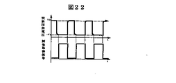
上記の操作を1つの電子源で実現させるには、試料印加電源9と電子源電源23との相対電圧、すなわち電子源電源23あるいは試料印加電源9の印加電圧を周期的に切り替えることにより実現できる。例えば、図22に示すように、試料印加電源電圧を基準として電子源電源23に印加する電圧を周期的に切り替えるとする。まず、ステージ8あるいは照射系偏向器5を用いて、所定の検査領域に電子線を移動し、試料を正帯電させる電圧+Vb、例えば500Vを電子源電源23から電子源1に印加して一定時間照射することにより、所定の検査領域を正帯電させる。次に、電子源電源23に供給する電圧を画像取得する電圧−Vpに切り替えて電子源1に印加することにより、試料ポテンシャルに対し−eVpほどエネルギーの小さいビームを所定の検査領域に照射して、試料が正帯電した状態で一定時間画像を取得することができる。検査領域を移動するたびにこの操作を周期的に繰り返すことにより、試料を正帯電させた状態で連続して画像を取得することができる。
【0117】
(実施例6)
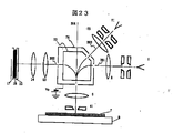
試料直前で引き戻されて結像する電子線を発生する電子源とは別に、一次電子線に対する二次電子の放出比が1より大きいエネルギーの電子線を同時に照射するための電子源を新たに配置することで、試料を正帯電させると同時に画像を取得することが可能となる。図23に本実施例の構成を示す。
電子源1はウェハ7よりわずかに正電位に置かれており、電子源1から放出された入射電子線301はウェハ7の直上で引き戻されて反射電子線302となる。一方、第二の電子源71とウェハ7とは約500Vの電位差を持ち、第二の電子源71から放出された電子線303は試料に500eVのエネルギーで照射される。磁界プリズム(magnetic prism)73はVsの電圧にフローティングされたシールド電極74に覆われており、磁界プリズム73に入射する電子線はeVsのエネルギーだけ減速されて偏向を受け、磁界プリズム73を出射する電子線はエネルギーeVsだけ加速される。例えば、電子源1から出射した電子線301は、磁界プリズム73の直前で約500Vまで減速され、磁界プリズム72に入射する。一方、第二の電子源71から出射した電子線303は、磁界プリズム73に入射する直前に約1000Vまで減速され、磁界プリズム73に入射する。ここでプリズム内の磁束密度を5ガウスに設定すれば、電子線301はサイクロトロン半径150mm、電子線302は半径約210mmの軌道を描いて同一光軸304 に入射することにより、同一視野を異なるエネルギーの電子線で照射することができる。試料の直上近傍で引き戻された反射電子線302は、磁界プリズム73に入射して入射電子線と反対方向に偏向された後、中間レンズ(intermediate lens)13、投影レンズ(projection lens)14を通じて、蛍光版15上に結像される。
<実施例7>
図24に示す本実施例は、第二の電子源201および第二の照射レンズ202を配置して、第二の電子源201から出射した電子線303を円孔レンズ電極41下部に衝突させて発生した弾性散乱電子304を試料7に照射できるような構成である。円孔レンズ電極41下部に電子線を衝突させて発生した弾性散乱電子304の光軸方向のエネルギー成分が円孔レンズ電極41と試料7の間に印加される電圧で減速されるエネルギーより大きければ、弾性散乱電子304は試料面に達する。例えば、弾性散乱電子304の方向分布が光軸402に対し30度傾斜した方向にピークを持っていれば、第二の電子源201から生じる電子線303の加速電圧としては、円孔レンズ電極41と試料7の間に印加される電圧に500V/COS30°= 577V加えた電圧を与えてやれば、弾性散乱した電子304のピーク成分は試料7に約500Vの加速電圧で照射できるので、試料7を正帯電させることができる。電極下部に衝突させる電子線303の角度および位置は、弾性散乱電子304が減速電界で軌道(trajectory)を変えることを考慮して、結像させるための照射電子線301と照射位置がほぼ同じくなるように設定するが、アライナ204にビーム傾斜機能とビーム位置移動機能を持たせ、照射位置が調整できるようにしている。
<実施例8>
図25に示す本実施例は、試料を帯電させる手段として光源251を配置して、試料に光線252を同時照射できるような構成である。試料7に試料7を構成する物質の仕事関数より大きなエネルギーの光線を照射すれば、試料7から光電子が放出されることによって、試料7を正帯電させることができる。図26の断面図は、シリコン(Si)上に絶縁膜(SiO2膜)が形成されたウェハにコンタクトホール加工後タングステン(W)プラグが埋め込まれた試料7を示したものである。中央部のプラグ底部にSiO2の残渣に起因する高抵抗のオープン欠陥が存在する。
図26(a)は絶縁膜311を正帯電させる場合の初期照射の状態を示したものである。試料7の電位に対して電子源1の電位は+Vpの正電位に置かれ、電子源1から出射した電子線301は円孔電極41と試料7の間で減速されて、試料の直上近傍で方向を変えて反射電子線302となる。SiO2の仕事関数はおおよそ9eVであるので、光線252として9eVよりエネルギーの高い紫外線を同時に試料に照射すれば、SiO2で構成される絶縁膜311は光電子305を放出するので、図26(b)に示すように、絶縁膜311が正帯電して絶縁膜311直上近傍の等電位面314は湾曲するようになる。絶縁膜311の正帯電がさらに進行すると、入射電子線301の一部が絶縁膜311に達するようになり、絶縁膜311からの光電子305の放出量と入射電子線301の絶縁膜311への到達量が等しくなるような平衡状態で絶縁膜311の正帯電電位は安定する。この状態で反射された電子線302を結像すると、絶縁膜311の部分が暗くなるとともに、絶縁膜近傍の電位歪を反映するような像が形成されるので、パターン正常部と異常部とのコントラストが高い像を取得できる。光源251から出射した光線252の光軸404と照射電子線301の光軸402とは、試料上で概一致するように調整されているが、光線252の試料7での照射領域を照射電子線301の照射領域より広く取ることによって、ステージを移動させて連続的に画像を取得する際には、一定時間光線252を照射して試料を正帯電させた状態で試料7に照射電子線301を照射することができる。同時に発生した光電子305は反射電子線の光路内に配置されたコントラストアパーチャ12により吸収させることができるので、コントラストの高い結像電子像を得ることができる。
<実施例9>
本実施例では、ビームセパレータ3として、E×B型偏向器(E×B deflector)2組と球面型の静電型プリズム(electrostatic prism)2組を組み合わせて、入射電子線と反射電子線を分離する構成を用いた。その構成図を図27に示す。この構成では試料から反射した反射電子線はE×B型偏向器54を直進するように設定されており、入射電子線301は2組のE×B型偏向器を逆方向に動作させるとともに、2組の静電型プリズムも逆方向に動作させてレンズ結像条件を最適に選ぶことにより、照射系および結像系の収差を低減できる構成である。さらに、結像系および照射系をステージに対して垂直に並べられる構成となっているので、機械振動などによる電子光学系への影響を最小限に低減できる効果がある。以下、構成の詳細を説明する。試料から反射した反射電子線に対しては、E×B型偏向器54は磁界と電界の作用が打ち消すように動作して、反射電子線はE×B型偏向器54内を直進する。さらに、反射電子線の像点をE×B型偏向器54近傍に置くことによりE×B型偏向器54で発生するレンズ収差を小さくするようにしている。電子源から出た入射電子線301はコンデンサレンズによって光軸401上の結像点403に結像した後、E×B型偏向器51に入射して、約15度偏向される。偏向した入射電子線301は静電型プリズム52に入射して、円形軌道を描き、所定の角度回転しながら、集束レンズ作用を受ける。静電型プリズム52を出た入射電子線301は静電型プリズム53に入射し、反対方向に回転しながら集束作用を受ける。静電型プリズム53を出射した入射電子線301はE×B型偏向器54に入射し、E×B型偏向器51とは反対方向に約15度偏向を受けて、照射系の対物レンズ光軸402に入射して、結像点404に結像する。ここで、静電型プリズム51と結像点403との間の距離と静電型プリズム53と結像点404の間の距離をほぼ等しく置き、静電型プリズム51をほぼ平行で出射した入射電子線301が静電型プリズム53にほぼ平行に入射する条件になるように上記静電型プリズムの動作条件を選べば、この2組の静電型プリズムの収差はほぼ補正される。
たとえば、回転角200度、半径50mmの静電型プリズムに静電型プリズム51とコンデンサレンズ結像点403との間の距離約170mmから入射エネルギー10keVで入射電子線301が入射するとプリズム出射時には入射電子線301はほぼ平行となり、静電型プリズム54出射時にはほぼ対称の位置、静電型プリズム53と結像点404の間の距離約170mmの位置に集束する。この条件では、静電型プリズム51と静電型プリズム54の収差は打ち消しあってほぼ零になるので、試料に高輝度な入射電子線301を照射することが可能となる。<実施例10>
本実施例は試料高さや傾斜角が変動しても正確な検査ができる手段を設けたものである。大口径のウェハは、ウェハのそり等による変形により試料の高さや傾斜角度が面内で大きく変動してしまうので、試料高さが変動しても結像位置が変動しない手段と、試料傾斜角が変動しても常に試料面に垂直に入射電子線が入射するための手段が必須である。
図28はウェハが傾斜した場合にも、試料に垂直に入射電子線301が入射するための制御方法を説明するものである。
xyz直交座標系において、z方向を光軸に取り、通常はz=0のxy平面内にある試料表面が、z=0を通り、x方向にθだけ傾斜している面内にあるとすると、試料7と円孔レンズ41電極間の距離をLと置けば、電界強度のz方向成分Ezおよびx方向成分Exはそれぞれ、Ez≒E、Ex≒(1−z/L)Eで近似される。x方向およびz方向について電子の運動方程式を解けば、入射電子線301が試料7に一番近づいた状態で試料7にほぼ垂直に入射する条件は、円孔レンズ41を通過する角度βが
【0118】
【数1】
さらに、円孔レンズ41の焦点距離は、円孔レンズ41の円孔の直径がLに対して十分小さければf=4Lと近似できるので、このような条件においては、円孔レンズ41に入射する入射電子線301の角度を2sinθだけ傾ければ良いことがわかる。
そこで、たとえば、対物レンズ7と円孔レンズ41の間にアライナ42を配置して、試料がx方向にθ傾いた場合には、概2θだけ傾斜するように作用させれば、常に試料に垂直に入射電子線301を照射することができる。ここで、このアライナ42は入射電子線301と反射電子線302とで同じ方向に作用するように静電型のアライナを用いるほうが望ましい。
試料高さの変動に対する補正は以下のように行う。円孔レンズ41の焦点距離fは、f=4Lで近似され、試料の下L/3の位置に試料から反射した反射電子線の虚像(virtual image)が形成される。対物レンズ7の物面位置(object plane)はこの円孔レンズ41の虚像位置(virtual image plane)となるので、試料高さが変動すると円孔レンズ41の虚像位置が変動し、対物レンズ(objective lens)7の像面位置も変動してしまうことになる。そこで、試料高さからLを算出して、円孔レンズの虚像位置すなわち対物レンズの物面位置を算出して、常に対物レンズの像面位置が一定となるように対物レンズの強度(lens excitation)を制御すれば,試料高さが変動しても常に像がボケないように制御することができる。
半導体ウェハ7の高さ分布は、あらかじめ検査前にウェハ内の数十点以上の高さ計測点について、高さ測定器26などの高さ計測手段を用いて計測される。試料の特定点の傾斜角は隣接した高さ計測点との高度差を、隣接した高さ計測点までの距離で割ることにより求めることができる。隣接した複数の高さ計測点との傾斜角計測値の平均を取ることにより、計測値の制度を向上させることができる。任意の検査位置に対応する傾斜角データは上記高さ測定点の傾斜角データを補間することにより求めることができる。検査時にはこの検査位置座標に対応したウェハ傾斜データに基づいて、アライナ42の強度を制御することにより、ウェハ面内で常に試料に垂直に入射電子線301を照射することが可能となる。
【0119】
【発明の効果】
本発明の実施例によれば、電子ビームを用いて、半導体装置等の試料表面の微細なパターン欠陥およびオープン、ショート、リーク等の電気的欠陥を高感度、高分解能で、かつ高速に画像化して検査することのできる検査方法および検査装置を実現する。
【図面の簡単な説明】
【図1】本発明の第1の実施例になる検査装置の概略構成を示す図。
【図2】本発明の原理を説明する図。
【図3】本発明の原理を説明する図。
【図4】本発明で得られる欠陥の画像例を示す図。
【図5】従来例において画像形成に利用できる電子の効率を説明する図。
【図6】従来例において画像形成に利用できる電子の効率を説明する図。
【図7】従来例と本発明の画像形成に利用できる電子の効率の違いを説明する図。
【図8】従来例と本発明のコントラスト(a)と検査時間(b)を比較する図。
【図9】本発明の第1の実施例の構成を説明する図。
【図10】電子のエネルギー幅と欠陥検出感度の関係を説明する図
【図11】本発明の第1の実施例における予備帯電制御装置の原理を説明する図。
【図12】本発明の第1の実施例における予備帯電制御装置の一構成を説明する図。
【図13】本発明の第1の実施例における予備帯電制御装置の他の構成を説明する図。
【図14】本発明の第1の実施例における画像信号検出手段を説明する図。
【図15】本発明の第2の実施例における画像信号検出手段を説明する図。
【図16】本発明の第3の実施例における画像信号検出手段を説明する図。
【図17】本発明の第4の実施例における電子光学系の構成を説明する図。
【図18】本発明の第5の実施例の構成を説明する図。
【図19】本発明の第5の実施例における帯電制御を説明する図
【図20】本発明の第5の実施例における画像取得領域と電子線照射領域を説明する図。
【図21】本発明の第5の実施例における欠陥の画像例を示す図。
【図22】本発明の第5の実施例における試料の印加電圧の制御を説明する図。
【図23】本発明の第6の実施例を説明する図。
【図24】本発明の第7の実施例を説明する図。
【図25】本発明の第8の実施例を説明する図。
【図26】本発明の第8における帯電制御を説明する図。
【図27】本発明の第9の実施例を説明する図。
【図28】本発明の第10の実施例を説明する図。
【符号の説明】
1:電子源、2:コンデンサレンズ、3:ビームセパレータ、4:絞り、5:照射系偏向器、6:対物レンズ、7:試料(ウェハ)、8:ウェハ移動ステージ、9:電源、10:結像系偏向器、11:結像レンズ、12:コントラストアパーチャ、13:拡大レンズ、14:拡大レンズ、15:蛍光板、16:光ファイバー束、17:CCD、18:画像記憶部、19:画像記憶部、20:演算部、21:欠陥判定部、22:モニタ、23:加速電源、24:走査信号発生器、25:対物レンズ電源、26:試料高さ測定器、27:ステージ位置測定器、28:ビーム制御系、29:制御計算機、30:ステージ制御系、31:光学顕微鏡、32:予備帯電制御装置、101:電子光学系、102:試料室、103:画像検出部、104:画像処理部、105:制御部、201:電子銃、202:コンデンサレンズ、203:ビームセパレータ、205:偏向器、206:対物レンズ、207:試料(ウェハ)、208:ウェハ移動ステージ、211:結像レンズ、213、214:拡大レンズ、222:SEM用コンデンサレンズ、228:ビーム制御系、232:予備帯電制御装置、233:SEM用対物レンズ、243:ビームセパレータ、252:試料室、263:画像検出部。[0001]
TECHNICAL FIELD OF THE INVENTION
The present invention relates to a method and an apparatus for inspecting a surface state of a sample (such as a semiconductor device).
[0002]
[Prior art]
As a method of detecting a defect of a circuit pattern formed on a wafer by a comparative inspection of an image in a manufacturing process of a semiconductor device, a so-called SEM method in which a point-shaped electron beam is scanned is used. Methods for comparing and inspecting patterns are described in JP-A-59-192943, "J. Vac. Sci. Tech. B, Vol. 9, No. 6, pp. 3005-3009 (1991)", and "J. Vac.Sci.Tech.B, Vol.10, No.6, pp.2804-2808 (1992), SPIEVol.2439, pp.174-183, and JP-A-05-258703. ing.
[0003]
These techniques are used for detecting minute etching residues or minute pattern defects having a resolution equal to or lower than the resolution of an optical microscope, and detecting electric defects such as non-opening defects of minute conduction holes. In these techniques, it is necessary to obtain a pattern image at a very high speed in order to obtain a practical inspection speed. Then, in order to secure an S / N ratio (signal to noise ratio) of an image acquired at high speed, a beam current of 100 times or more (10 nA or more) of a normal scanning electron microscope is used.
[0004]
Further, “Japanese Unexamined Patent Publication No. 7-249393”, “Japanese Unexamined Patent Publication No. 10-1974627”, Japanese Unexamined Patent Application Publication No. 2000-340160, and “Japanese Unexamined Patent Application Publication No. 11-108864” The semiconductor wafer is irradiated with an electron beam, and is reflected without being irradiated (imping?) On the wafer due to formation of back scattered electrons, secondary electrons, or a reversing electric field (primary field). (Reflect) Describes an apparatus for performing high-speed inspection by a so-called projection method such as forming an image of electrons by a lens.
[0005]
A mirror microscope is known as a technique for obtaining an image of the outermost surface of a sample by applying a potential to the sample to create a situation in which the sample is not irradiated with an electron beam but is reflected by an electric field near the surface, thereby obtaining an image of the outermost surface of the sample (for example, , "Rheinhold Godhardt, ADVANCES IN IMAGING AND ELECTRON PHYSICS, VOL. 94, pp. 81-150").
[0006]
[Problems to be solved by the invention]
In the conventional inspection technique using the above-described electron beam, the following problems remain in the SEM method and the projection method of reflected electrons and secondary electrons.
[0007]
First, in the case of the SEM method, the electron beam is made to have a larger current than that of a general SEM in order to form an image maintaining an S / N ratio that can be inspected. However, since the "point beam" is scanned in a plane (two-dimensionally) on the surface of the sample by narrowing the electron beam into a point, there is a limit in increasing the speed (reducing the inspection time).
[0008]
In addition, there is a limit in increasing the current of the electron beam due to the brightness of the electron source to be employed, a space charge effect, and the like. For example, to obtain a resolution of about 0.1 μm, the theoretical limit of the electron beam current is about several hundred nA, and in practice, only about 100 nA can be used. The S / N ratio of an image is determined by the number of electrons used to form an image, that is, the product of the beam current value and the time required for image acquisition. In order to secure an S / N ratio of an image in which the image processing can normally operate, when the beam current value is 100 nA and 0.1 μm, the area of the sample surface is 1 cm. 2 Requires more than 100 seconds to test
[0009]
On the other hand, in the projection method, an electron beam having a larger current can be irradiated at a time than in the SEM method, and an image can be acquired at a time. Therefore, it can be expected that an image can be formed at an ultra-high speed as compared with the SEM method. However, the emission angle distribution of the secondary electrons is spread over a wide angle, and the energy is also spread at about 1 to 10 eV. It is reported in LSI Test Symposium / 1999 Proceedings, P142 that sufficient resolution cannot be obtained unless most secondary electrons are cut off when forming an enlarged image of a sample by forming such electrons. It can be easily determined from FIG. 6 described above. This shows the negative sample applied voltage for accelerating the secondary electrons emitted from the sample and the imaging resolution of the secondary electrons. According to this, when the sample applied voltage is -5 kV, the resolution is approximately 0.2 μm.
[0010]
Then, not all the emitted secondary electrons can be used for image formation. For example, in the calculation of the cited document, a beam having an opening angle of 1.1 mrad or less is used on the image plane after passing through the objective lens. . The secondary electrons within the range of the opening angle are only about 10% of the whole. Furthermore, the energy width of the secondary electrons used for imaging is calculated at 1 eV, but the energy width of the emitted secondary electrons is actually emitted with a width of several eV or more. Side tails exist up to about 50 eV. When only electrons having an energy width of at most 1 eV are extracted from the secondary electrons having such a wide energy distribution, the number is further reduced to a fraction.
[0011]
As described above, even if an image is collectively formed by irradiating a large current with an electron beam as an area beam, it is difficult to secure the S / N ratio of the image because the ratio of electrons that can actually contribute to image formation is low. Therefore, it is impossible to shorten the inspection time as much as expected. Similarly, in the case of using the backscattered electrons, the emission amount is smaller by two orders of magnitude than the irradiation beam current, and it is difficult to achieve both high resolution and high speed as in the case of the secondary electrons.
[0012]
Regarding the above-mentioned mirror microscope technology, there has been no report on a method or an apparatus for applying this technology to inspection of a semiconductor wafer. In addition, there is no restriction on the directionality of the trajectory of the electron beam directed to the sample, and the electron beam is irradiated to the sample at a wide angle, and the resolution is about sub-μm, which is insufficient for observing the current semiconductor. Was.
[0013]
The present invention has been made in view of the above points, and has as its object to provide a defect inspection method and a defect inspection apparatus for detecting a defect portion in a pattern formed on a wafer at high resolution and at high speed. And
[0014]
[Means for Solving the Problems]
The object of the present invention can be achieved by the following method.
[0015]
That is, a plurality of irradiation areas (area areas) on the surface of the sample are not "point beams", but "area beams (seat beams)" (plane-shaped electrons) having a two-dimensional spread. Beam). A negative potential is applied to the wafer. This negative potential is set to a value such that most electron beams are returned near the outermost surface of the wafer. Specifically, the potential is set to a negative potential higher by 0.5 V to 5 V than the potential of the electron source (cathode or electron source). This causes the electrons that have been pulled back to form an image (hereinafter, electrons that have been pulled back by the electric field without colliding with the sample will be referred to as “retracted electrons” or “mirror electrons”). Then, enlarged images of the plurality of irradiation regions are sequentially formed, the enlarged images of the plurality of irradiation regions are converted into electrical image signals, and the image signals of the plurality of irradiation regions are compared with each other. This makes it possible to detect a pattern defect in each of the irradiation regions with high resolution and at high speed.
[0016]
As a typical configuration example of the present invention, first, a pattern defect inspection method according to the present invention applies a planar electron beam having a two-dimensional spread to a plurality of irradiations of a sample surface to which a negative potential is applied. Irradiating the plurality of irradiation areas sequentially to form an image of the electrons drawn back near the surface of the sample without colliding with the sample, thereby sequentially forming enlarged electron images of the plurality of irradiation areas, By converting the enlarged electronic image of the region into an electric image signal and comparing the image signals of the plurality of irradiation regions with each other, a pattern defect formed on the sample is detected. I do. Here, the planar electron beam is configured to irradiate each of the plurality of irradiation regions so that the traveling directions thereof are substantially parallel to the sample surface and are incident substantially perpendicularly.
[0017]
In addition, the wafer defect inspection apparatus according to the present invention includes a first electron optical system that irradiates an electron beam from an electron source as a planar electron beam having a two-dimensional spread to a plurality of irradiation regions on a sample surface; Means for generating an electric field such that electrons forming the electron beam irradiated toward the sample are drawn back near the outermost surface of the sample, and forming an image of the electrons drawn back from the plurality of irradiation areas to form an image. A second electron optical system for forming enlarged images of the plurality of irradiation regions; image signal detecting means for converting the enlarged images of the plurality of irradiation regions into electrical image signals for detection; Image signal processing means for comparing image signals of a plurality of irradiation regions on the sample surface with each other to detect a pattern defect in each irradiation region, and detecting a pattern defect formed on the sample It is characterized in that the cormorants configuration.
[0018]
Further, the pattern defect inspection apparatus according to the present invention comprises: an electron beam irradiation optical system for irradiating an electron beam from an electron source as a planar electron beam having a two-dimensional spread to a plurality of irradiation regions on a sample surface; Means for generating an electric field such that all or a part of the electrons forming the electron beam are pulled back immediately before colliding with the surface of the sample, and forming an image of the electrons drawn back from the plurality of irradiation regions to form an image. An imaging optical system for forming an enlarged image of a plurality of irradiation regions; and a sample for mounting the sample and moving the sample so that each of the plurality of irradiation regions is irradiated with the electron beam. A moving stage, an image signal detecting unit that converts each of the enlarged images of the plurality of irradiation areas into an electric image signal and detects the image signals, and converts the detected image signals of the plurality of irradiation areas on the sample surface to each other. Compare to, and characterized by having an image signal processing means for detecting a pattern defect by determining whether differences exist above a predetermined threshold at each irradiation area.
[0019]
Further, the pattern defect inspection apparatus according to the present invention is characterized in that an electron optical system for acquiring a SEM image of the sample is provided at a predetermined position in the moving direction of the sample moving stage.
[0020]
The first electron optical system or the electron beam irradiation optical system is disposed between an electron gun that generates an electron beam, a condenser lens that focuses the electron beam emitted from the electron gun, and the condenser lens and the sample. An objective lens and an electron beam deflecting mechanism. The condenser lens focuses the electron beam on a focal plane on the electron source side of the objective lens, and the traveling direction is substantially parallel to the sample surface. A planar electron beam that is incident substantially perpendicularly is formed to irradiate a plurality of irradiation areas on the sample surface.
Further, when a circular electrode (aperture electron) facing the sample largely acts as an electron lens, the objective lens focuses the electron beam on a focal plane of a circular lens (aperture lens). With this arrangement, it is possible to form a planar electron beam that is incident substantially perpendicularly with the traveling direction being substantially parallel to the sample surface.
[0021]
The means for generating an electric field such that electrons irradiated toward the sample are pulled back on the outermost surface of the sample is constituted by, for example, a power supply for applying a predetermined negative potential to a conductive sample holder that holds the sample. In the case of a sample such as a semiconductor having an insulating film on its surface, a second electron gun is provided at a position distant from the optical axis of the electron beam for image formation, and pre-charge control for irradiating the sample with electrons before image formation. Means. Further, a grid is provided between the sample and the second electron gun to which a potential can be applied, and means for irradiating the sample with electrons using the second electron gun while controlling the voltage applied to the grid is provided.
In order to inspect a conduction defect such as a short circuit or a disconnection of a pattern of a semiconductor sample, a defective pattern can be detected by detecting a voltage difference between a normal pattern and a defective pattern caused by the preliminary irradiation. However, if the resistance of the defect pattern is relatively small, the accumulated charges escape to the surroundings, so that the potential difference between the normal pattern and the defect pattern caused by the preliminary irradiation is not maintained for a long time. In this case, there should be provided a means for injecting electrons into the sample to generate a potential difference between the normal pattern and the defect pattern, and a means for irradiating the electrons which are reflected and imaged without hitting the sample at almost the same place and almost simultaneously. Is required. In order to meet the demand for negatively charging the defective pattern and the insulating film pattern, the sample is irradiated with an electron beam having an extra energy eVn with respect to the sample potential so that the insulator is charged to the negative voltage Vn and stabilized. When the image is obtained by the above, the image can be obtained in a state where the defective pattern and the insulator pattern are negatively charged. The requirement for positively charging the defective pattern and the insulating film pattern can be solved by simultaneously or alternately irradiating a beam for acquiring an image and an electron beam or light for positively charging the sample.
[0022]
Further, by setting the sample moving stage (sample stage) so as to continuously move the sample at substantially the same speed, it is possible to realize high-speed defect inspection. In this case, it is needless to say that by monitoring the position of the sample moving stage, it is necessary to control the electron beam irradiation area on the sample surface to be the same for a predetermined time. That is, a stage position measuring mechanism that measures the position of the continuously moving sample moving stage in real time is provided, and a position change that occurs during the stage movement due to the continuous movement is measured by the stage position measuring mechanism. By feeding back to the electron beam deflecting mechanism of the beam irradiation optical system, the positional relationship between the electron beam and the sample moves at a substantially constant speed in a predetermined direction.
[0023]
Further, the image signal detecting means projects an enlarged electronic image of the irradiation area formed by the second electron optical system or the imaging optical system onto a phosphor screen (optical screen) to thereby form an optical image (optical image). ), And forms this optical image on an optical image detecting element via an optical lens or an optical fiber. Alternatively, the magnified electronic image formed by the optical system may be directly formed on an image sensing element having sensitivity for electron. Note that a charge-coupled device (CCD) or a device that integrates and outputs a time-delayed optical signal (TDI: Time Delayed Integration sensor) can be used as the image detection device. The reading of the detection signal from the image detecting element is performed in a method of reading in multiple channels in parallel.
[0024]
BEST MODE FOR CARRYING OUT THE INVENTION
Hereinafter, embodiments of the present invention will be described in detail with reference to the drawings.
[0025]
(Example 1)
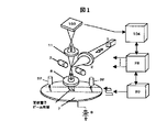
FIG. 1 shows the minimum components necessary for explaining the operation principle of the present invention. The electron beam emitted from the
[0026]
A negative potential substantially equal to or slightly higher than the acceleration voltage of the electron beam is applied to the sample (wafer) 7 by the
[0027]
The retracted electron beam is converged by the objective lens 6, and the
[0028]
In order to detect a defect in the semiconductor pattern formed on the
[0029]
When an insulator exists on the surface of the
[0030]
Next, the principle of imaging defects on the wafer surface under the condition that the electron beam is pulled back on the surface of the
[0031]
FIG. 2 schematically shows a state in which the
[0032]
FIG. 3 shows a simulation result of the
[0033]
The potential of the electron source was +1 eV based on the potential of the wafer. That is, when the potential applied to the wafer is 0 V, the electron beam is reflected on the +1 V equipotential surface and becomes an imaging electron beam. In this case, it is shown that the electron beam is strongly affected by the disturbance of the equipotential lines formed by the patterns having different potentials at the center, and the vertically incident beam is reflected at a large angle.
[0034]
FIG. 4 shows the calculated density of the electron beam pulled back by the electric field on the wafer surface. As shown in the “structure” column in the figure, the portions arranged in 3 × 3 are conductive materials, and only the central potential is different from the surrounding by 1V. The lower figure shows the electron beam trajectory calculation with the energy width (ΔE) of the electron beam set to 2 eV in this case, and plots the electrons returned from the wafer surface. Higher dot density indicates higher electron density. It is shown that electrons are concentrated in the central part and there is a high electron density part, which indicates that a change of 1 V of a 70 nm fine pattern can be detected by the principle described with reference to FIG. 2, that is, a conduction failure defect can be detected. ing.
[0035]
Here, a description will be given of how the present invention improves the inspection speed by an order of magnitude as compared with the method of scanning a point beam or the method of imaging secondary electrons. In the case of an image forming apparatus using an electron beam, what limits the speed of image acquisition ultimately results in an S / N ratio required for an image. The S / N ratio of an image is determined by the number of electrons used to form the image. Also, the required S / N ratio is determined by the magnitude of the contrast that the defect to be detected causes in the image. That is, if the defect contrast is the signal C, the noise needs to be smaller than that. The noise N is defined by the 3σ value of the signal. The σ value is determined by the shot noise of the number of irradiated electrons, and is the square root (√S) of the number of electrons S irradiated per pixel (pixel). Therefore, the noise N is 3√S.
[0036]
In the case where the electron beam collides with the
T = (0.01 / x) 2 ・ T
= (1.6e-19 · 0.01 2 ・ (3√2) 2 ) / (I · η · C 2 ・ Pix 2 …… (1)
Note that t = ((1.6e-19 · (3√2) 2 ) / (I · η · C 2 )) ・ (X 2 / Pix 2 )
Here, t is the time during which the electron beam must stay at the same location to make the noise smaller than the contrast C. That is, in the case of the SEM method, this is the time during which the electron beam probe irradiates one pixel. In the case of surface beam irradiation, it is a time during which the beam needs to be directed to a certain point, and this time is called a shot time.
[0037]
Pix is the required resolution, x is the length of one side of the area beam (same as the pixel size or Pix in the case of the SEM type), I is the beam current, and η is the efficiency of electrons that can be used for image formation. On the other hand, in the present invention, since the electron beam does not collide with the surface of the
T = (0.01 / x) 2 ・ T
= (1.6e-19 · 0.01 2 ・ (3) 2 ) / (I · η · C 2 ・ Pix 2 ) (2)
In addition, t = ((1.6e-19 · (3) 2 ) / (I · η · C 2 )) ・ (X 2 / Pix 2 )
Here, η and C in each system are estimated. In the case of the SEM method, almost the same number of secondary electrons as the irradiated electron beam are emitted, and almost 100% of the emitted secondary electrons can be taken into the detector.
[0038]
On the other hand, in the secondary electron projection system in which a planar electron beam is irradiated on the
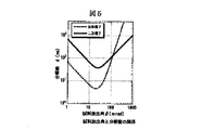
[0039]
FIG. 5 shows the resolution of an image with respect to the emission half angle β of secondary electrons or reflected electrons that contribute to image formation. That is, it is the half-open angle of the electrons taken into the imaging system. For example, it shows that the resolution when an image is formed by secondary electrons having an emission angle of 100 mrad or less is about 100 nm. As the calculation conditions, the energy of the electrons applied to the wafer is 500 eV, the surface of the wafer is under a strong electric field of 5 kV / mm, and the energy width of the secondary electrons is 5 eV. Although the energy distribution of the secondary electrons spreads over 10 eV or more, only the component of ± 2.5 eV centered on the emission energy of 2 eV is used for imaging. This corresponds to about 1/2 of all secondary electrons.
[0040]
The energy width was set to 1 eV, considering only the elastic scattered electrons as the reflected electrons. From these figures, it is necessary to set the emission angle to 25 mrad in order to make the resolution of the secondary electrons, for example, 40 nm. In this case, the probability that the secondary electrons are scattered within the emission angle β is about 0.1%. . Assuming that the secondary electron emission efficiency (yield) (the ratio of the number of secondary electrons to the number of irradiated electrons) is approximately 1, η in the case of the secondary electron imaging type is ×× 0.001 × 1 = 0. 0005.
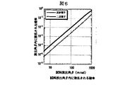
[0041]
On the other hand, in order to set the resolution to 40 nm in the case of backscattered electrons, the sample emission angle (β) is 80 mrad, and the probability of the presence of backscattered electrons within that angle is 0.2% from FIG. The emission efficiency of the backscattered electrons (the ratio of the number of backscattered electrons to the number of irradiated electrons) is based on the reference document “Image Formation in Low-Voltage Scanning Electron Microscopy, SPIE, Bellingham, p. It is about 0.02 to 0.03. Therefore, η in the backscattered electron imaging type has a considerably small value of 0.002 × 0.025 = 5e−5.
[0042]
On the other hand, in the present invention, since the electron beam is bounced vertically upward on the flat wafer surface, the opening angle of the beam is very small (several mrad), which is equal to the angular variation of the irradiation beam. FIG. 7 is an explanatory diagram for further understanding the description so far.
[0043]
As shown in the left diagram of FIG. 7, the secondary electrons are emitted from the sample into a vacuum with a spread of 180 degrees, whereas in the present invention, as shown in the right diagram, all the electrons are almost right above. As a result, the irradiated electrons can be effectively used as an image. On the other hand, when the surface has irregularities or a potential distribution, it travels upward at a certain angle instead of the vertical direction. In this case, the ratio of electrons directly contributing to the image formation is reduced, but the change in the angle itself is a factor for forming an image on the wafer surface, so that the contrast is increased. In other words, this is equivalent to increasing the contrast C of the defect, which is advantageous for defect detection.
[0044]
After all, in the present invention, η and C are linked, and if η is limited, C will increase accordingly. Strictly speaking, the type of pattern differs depending on the type of defect. In this case, however, a signal that can be detected as an image at a defective portion is の of all electrons. The remaining half signal contributes to the contrast. Therefore, η = 0.5 and C = 0.5.
[0045]
Table 1 summarizes the above.
[0046]
[Table 1]
[0047]
Next, the configuration of an embodiment of the present invention will be described in detail. FIG. 9 shows a configuration of an inspection apparatus according to one embodiment of the present invention. The inspection apparatus according to the present embodiment is roughly divided into an electron
[0048]
First, the electron
[0049]
As a result, a planar electron beam which is oriented in a direction perpendicular to the surface of the
[0050]
Even if the front focal plane of the objective lens and the crossover position cannot be completely matched, there is no problem as long as it is within a certain allowable range. Also, the magnitude of the crossover is ideally zero, but actually has a finite magnitude due to aberrations of the electron gun and the condenser lens. There is no problem if this size is within a certain allowable range. In the electron optical system in which the position of the crossover was accurately controlled and the aberrations of the electron gun and the condenser lens were sufficiently reduced, the spread of the incident angle on the sample could be suppressed to 0.5 mrad or less. The spread of the incident angle is one of the factors that determine the resolution of the enlarged image of the sample surface due to the mirror electrons, and is expressed by the following equation.
[0051]
r0 = β 2 ・ Zm… (3)
Here, r0 is the resolution determined by the spread of the incident angle, β is the maximum half angle of incidence, and Zm is the distance in which an electric field that pulls back electrons is generated.
[0052]
In this embodiment, β is 0.25 mrad and Zm is 5 mm. By substituting this into equation (3), r0 is 0.3 nm, which indicates that this embodiment does not affect the resolution. Therefore, the beam current can be further increased as needed.
[0053]
Note that even if the resolution is about 30 nm, it is considered to be sufficient for detecting a defect in a semiconductor. Therefore, if Zm is 5 mm, β can be tolerated up to 2.4 mrad. In this case, there is considerable margin in the deviation of the crossover position from the front focal plane of the objective lens and the size of the crossover.
[0054]
Assuming that the half angle of the beam opening on the front focal plane is α, the focal length of the objective lens is f, the displacement of the crossover is Δf, and the radius of the planar electron beam is X, the following equation is established.
[0055]
Δf = f · β / α (4)
α = X / (2f) (5)
From Equations (4) and (5), for example, when the focal length f of the objective lens is 10 mm and the size X of the planar beam is 40 μm, there is no problem even if the crossover position shift Δf is shifted by about 10 mm. This is approximately 40 μm when converted to a beam diameter at the front focal plane. In any case, it is understood that sufficient resolution can be obtained by disposing the crossover of the electron beam near the front focal plane of the objective lens.
[0056]
Here, the
[0057]
Further, as will be described later with reference to FIG. 10 as Example 2, in the case of an optical system in which the optical axis of the imaging lens and the optical axis of the objective lens 6 are arranged in a straight line, the electric field and the magnetic field are made to go straight, An E.times.B deflector is used to make the mirror electrons go straight and to deflect only the electron beam from above.
[0058]
To the
[0059]
The electron beam directed perpendicular to the surface of the
[0060]
In order to improve the contrast and resolution of the electronic image, a
[0061]
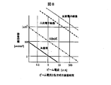
In the image forming principle of the present invention, the sensitivity and the resolution of an image for detecting a subtle difference in charge on the wafer surface are determined by the energy width of the planar electron beam. FIG. 10 shows the result of comparing the results by simulation. Assuming the same pattern as in FIG. 4, images obtained in two cases where the electron beam energy width (ΔE) is 2 eV and 4 eV were compared.
[0062]
According to this result, when an energy width of 4 eV is assumed, no contrast is observed in a portion having a different potential at the central portion of the pattern. In consideration of the progress of miniaturization of semiconductors, it is necessary to detect a difference in charged potential of about 1 V as a defect in a fine pattern as shown in FIG. Therefore, it is understood that the energy width of the electron beam used in the present invention is desirably 2 eV or less.
[0063]
As described above, in this embodiment using the Zr / O / W Schottky electron source, there is no problem because the energy width is 1.5 eV. For example, when an electron source with a larger energy width is used, an energy filter is provided on the optical path of the electron beam, and the electrons are emitted from the electron source until the image is finally formed. The energy width needs to be 2 eV or less. The energy filter is desirably provided between the electron source and the
[0064]
In the present invention, the electron beam does not collide with the
[0065]
However, in a defect inspection of a semiconductor pattern using an electron beam, a so-called electrical defect such as a continuity failure, a short-circuit of an object to be insulated, or a leak current larger than that of a normal part is called. There is a method in which a charged object is charged by irradiation with an electron beam and is detected based on a potential contrast of an SEM image generated by a difference in the potential.
[0066]
In order to detect such a defect with high sensitivity, the present invention includes a preliminary charging control device that irradiates an electron beam dedicated to charging control before acquiring an inspection image. If the inspection is performed after the
[0067]
FIG. 11 is a diagram illustrating the operation principle of the preliminary charging control device. The
[0068]
The secondary electrons have an energy of about 2 eV with reference to the potential of the surface of the insulating
[0069]
Since a
[0070]
FIG. 12 shows the configuration of a preliminary charging control device using a carbon nanotube electron source. The
[0071]
FIG. 13 shows a configuration of a preliminary charging control device using a LaB6 electron source. When a LaB6 electron source is used for a microscope, a crossover is formed immediately after electron emission using a Wehnelt electrode. In this case, since the light source does not need to be small, an extraction electrode 42 'is provided instead.
[0072]
In the
[0073]
In order to accurately measure the height of the semiconductor sample (wafer) surface, an optical sample
[0074]
Next, the settling time of the
[0075]
Next, the
[0076]
Next, the reading time of the image detecting element (CCD) will be described. In this embodiment, the charge accumulated in the
[0077]
In the present embodiment, the readout port of image data from the CCD is divided into 128 channels, and the system is configured to perform parallel and simultaneous readout on the 128 channels, so that the required readout time per pixel is 16 nsec, and the readout speed that can be sufficiently realized is achieved. And This is schematically shown in FIG.
[0078]
The number of channels for reading image data from the
[0079]
As described above, a sample area of 1 cm according to the conventional method when inspecting with a pixel size of 50 nm 2 In comparison with the required inspection time of about 400 seconds, a speedup of 80 times was achieved. In this embodiment, the time required for the inspection is determined by the signal read speed from the CCD element. Therefore, if a higher-speed data read method in the CCD element is realized in the future, a further increase in inspection speed is expected. it can.
[0080]
The
[0081]
The operation command and operation condition of each unit of the device are input and output from the
[0082]
Next, an actual inspection procedure will be described. First, a method of alignment using the
[0083]
Next, rotation correction is performed by the
[0084]
Next, the
[0085]
Further, the circuit pattern on the surface of the
[0086]
Next, the
[0087]
Furthermore, after a certain degree of rotation correction is performed, a higher-precision rotation correction can be performed using an electron beam image having a higher resolution than an optical microscope image and capable of obtaining a high-magnification image. Further, using this electron beam image, the inspection area or the same pattern area can be observed and confirmed / corrected with high magnification and high precision. However, when the entire surface (or a part) of the
[0088]
After the setting of the inspection conditions described above, a part of the inspection area on the surface of the
[0089]
When the setting of the area to be inspected and the defect determination conditions is completed by the above procedure, the inspection is actually started. At the time of inspection, the
[0090]
The irradiation area or irradiation position of the electron beam is constantly monitored by a stage
[0091]
Further, the surface height of the
[0092]
The electron beam is directed to the surface of the
[0093]
When performing a comparative inspection of patterns between adjacent chips A and B having the same design pattern formed on the surface of the
[0094]
In addition to the above method, it is also possible to adopt a method in which an electron beam image signal of a desired inspection area of a standard non-defective (no defect) sample is stored in the
[0095]
Then, at the same time as capturing the acquired image signal for the inspection area corresponding to the above into the
[0096]
However, according to the present embodiment, the image signal of the area known to be good (no defect) is stored in advance, and the stored image signal is compared with the image signal of the inspection target area. Such a defect occurring over the entire surface of the wafer can be accurately detected.
[0097]
The two image signals stored in the
[0098]
With the inspection method and the inspection apparatus described above, an image reflecting the information on the potential and the shape of the surface of the
[0099]
(Example 2)
In the first embodiment, since the area of the one-shot electron beam irradiation region is as large as 50 μm × 50 μm, the problem that distortion occurs at the periphery of the enlarged image of the semiconductor sample and the uniformity of the beam current density in the irradiation region May cause problems. If image distortion or non-uniformity of current density is fixedly generated, it can be corrected by changing the arrangement of the optical fibers of the
[0100]
In the present embodiment, the irradiation area of one shot is set to 5 μm square so that the distortion and the non-uniformity of the current density do not occur in the irradiation area of one shot. The irradiation electron beam current is 1 μA per shot. At this time, assuming that the electron beam irradiation time is an electron imaging efficiency η of 0.5, the irradiation time t per shot is 0.18 μsec from the above equation (1). After irradiating one irradiation area (5 μm square) with a shot time of 0.18 μsec, the electron beam is moved by the
[0101]
At this time, an enlarged image is obtained on the
[0102]
The
[0103]
As described above, when an image of a 50 μm square area on the surface of the
[0104]
In order to scan while irradiating the
[0105]
As the inspection proceeds according to the procedure described above, the sample surface is 1 cm 2 The time T required to sequentially form enlarged images of hits on the CCD is 0.72 sec. On the other hand, as in the case of the first embodiment, since it takes 125 μsec to read one image (image of a sample surface of 50 μm square) from the CCD, the sample surface area is 1 cm. 2 5 seconds are required. Since image formation and image signal readout in the CCD element are performed in parallel, the time required for inspection is the longer of the time required for image formation and the time required for image signal readout. In this embodiment, the time required for reading an image signal is longer than the time required for image formation, and is 1 cm. 2 5 sec per sample, and therefore, the surface area of the sample in this example was 1 cm. 2 The required inspection time for the hit is 5 seconds.
[0106]
In the above description, the case where the electron beam irradiation region of one shot is fixed to the size of 5 μm square is exemplified. However, the size of the electron beam irradiation region can be changed according to the pattern repetition pitch on the surface of the
[0107]
(Example 3)
In this embodiment, a time accumulation type CCD sensor is used as an element for converting a sample surface image into an electric signal. This element is called a TDI sensor, and is generally used in an optical inspection device. Other than that, it is the same as the case of the second embodiment. The operation concept of the TDI sensor will be described with reference to FIG.
[0108]
In the TDI sensor, the electric charge generated according to the intensity of the light received in each light receiving area is moved to the line in the x direction, and at the same time, the electric charge generated according to the intensity of the light received at the destination is moved. It works so that they are added sequentially. Then, when the light reaches the last line on the light receiving surface, the light is output to the outside as an electric signal. Therefore, by making the moving speed of the charge in the x direction and the moving speed of the image on the light receiving surface in the x direction the same, a signal during the movement of the image on the sensor is integrated and output.
[0109]
In the present embodiment, as in the case of the CCD sensors in the first to fourth embodiments, the signal reading is divided into 128 channels and read in parallel with each other, so that the reading speed is set to 4 M lines / sec. The size of the light receiving area was 64 pixels in the x direction and 2048 pixels in the y direction. The length of one line in the x direction corresponds to 50 nm on the sample surface, and the length in the y direction corresponds to about 100 μm. At this time, since an image having a length of 50 nm and a width of 100 μm is output at a speed of 4 M / sec, the continuous moving speed of the stage is set to the same speed (50 nm / 250 nsec = 200 mm / sec). As described above, the inspection area is moved in the x direction by moving the
[0110]
On the other hand, since the irradiation area of one shot is 5 μm square, it is necessary to move the irradiation area in the y direction by scanning the electron beam as shown in FIG. That is, it is necessary to scan the electron beam by 100 μm in the y direction while the
[0111]
As described above, in the present embodiment, since the stage moving speed determined by the signal output speed of the TDI sensor is 200 mm / sec, the inspection area can be sufficiently moved in the x direction by moving the stage. In addition, a sufficient time for scanning the electron beam in the inspection area in the y direction can be secured during that time. Further, in this embodiment, since the inspection speed is determined by the signal output speed of the TDI sensor, if the signal output speed is improved, an even higher-speed inspection can be realized.
[0112]
(Example 4)
This embodiment employs an electron optical system capable of acquiring an SEM image. FIG. 17 shows the configuration.
[0113]
For the
[0114]
This embodiment is characterized in that a high-resolution SEM image can be observed without taking out the
[0115]
This function can be used not only for observing the detected defect but also for confirming the pattern of the wafer before inspection, setting inspection conditions, alignment, and the like.
[0116]
(Example 5)
This embodiment employs a means for irradiating an electron beam which is injected into a sample to generate a potential difference between a normal pattern and a defective pattern, and an electron beam which is reflected and forms an image without hitting the sample at almost the same place and almost simultaneously. It is provided. FIG. 18 shows the configuration. The electron beam emitted from the
When an insulator is present on the surface of the
When an electron beam with an extremely low energy having an emission ratio of secondary electrons to a primary electron beam (the mean number of second electrons excited per incident electron) of less than 1 is applied to the insulator sample, the insulator sample becomes negatively charged (electron). It becomes negatively charged by accumulation. For example, with the irradiation energy of about 30 eV or less, SiO2 has a secondary electron emission ratio of less than 1 and is negatively charged. FIG. 19A shows the state of initial irradiation when the insulating
FIG. 21A shows that when a normal portion of a 70 nm square plug pattern of 3 × 3 rows is charged to 0 V, a defective portion of the center pattern is charged to −1 V, and the
Here, since the charging potential of the
In addition, all the
The standard of the time until the charging voltage of the insulating film is stabilized is as follows. Assuming a parallel plate capacitor having electrodes above and below the insulating film, the capacitance of the capacitor is defined as D, the electrode area is D, the dielectric constant of vacuum is ε0, and the dielectric constant of the insulating film is εr. (Capacitance of capacitator) C = ε0εrS / D For example, when an insulating film having a thickness of 0.4 μm and εr = 4 is irradiated with a current of 1 μA in an irradiation area of 20 μm square, the charging time to a voltage of 1 V is approximately 35 ns. Become When the insulating film is instantaneously charged and is not stable, as shown in FIG. 20, an electron beam irradiation area is set to be larger than the image acquisition area ahead of the inspection direction (scanning) direction, and the electron beam is preliminarily acquired before the image acquisition. Irradiation was adopted. Further, when the electron beam acquisition area is set to be substantially equal to the image acquisition area, the image acquisition area may be irradiated with an electron beam, and the image acquisition circuit may be controlled so as to acquire an image after charging is stabilized. .
Here, apart from the reflected
In order to detect an electrical defect, it is necessary to control the moving direction of electrons in the pattern depending on the bonding state with the substrate. Therefore, it is necessary to charge the insulating film not only negatively but also positively. In order to positively charge the insulating
FIG. 21B shows that, when the
The above operation can be realized by one electron source by periodically switching the relative voltage between the sample
[0117]
(Example 6)
Apart from an electron source that generates an electron beam that is pulled back immediately before the sample and forms an image, a new electron source for simultaneously irradiating an electron beam with an energy with an emission ratio of secondary electrons to the primary electron beam of more than 1 is newly arranged. By doing so, it becomes possible to obtain an image while simultaneously charging the sample positively. FIG. 23 shows the configuration of this embodiment.
The
<Example 7>
In the present embodiment shown in FIG. 24, the
Example 8
The present embodiment shown in FIG. 25 has a configuration in which a
FIG. 26A shows the state of initial irradiation when the insulating
<Example 9>
In this embodiment, as the
For example, when the
This embodiment is provided with a means for performing an accurate inspection even if the sample height or the inclination angle fluctuates. For a large-diameter wafer, the height and tilt angle of the sample fluctuate greatly in the plane due to deformation due to the warp of the wafer, so that the imaging position does not change even if the sample height fluctuates. It is necessary to provide a means for always allowing the incident electron beam to be perpendicularly incident on the sample surface even if the value fluctuates.
FIG. 28 illustrates a control method for causing the
In the xyz rectangular coordinate system, if the z direction is taken as the optical axis, and the sample surface normally in the xy plane at z = 0 is in a plane passing z = 0 and inclined by θ in the x direction, When the distance between the
[0118]
(Equation 1)
Further, the focal length of the
Therefore, for example, if the
The correction for the change in the sample height is performed as follows. The focal length f of the
The height distribution of the
[0119]
【The invention's effect】
According to the embodiment of the present invention, by using an electron beam, fine pattern defects on the surface of a sample such as a semiconductor device and electrical defects such as open, short, and leak are imaged with high sensitivity, high resolution, and high speed. An inspection method and an inspection apparatus that can be inspected by using the inspection method are realized.
[Brief description of the drawings]
FIG. 1 is a diagram showing a schematic configuration of an inspection apparatus according to a first embodiment of the present invention.
FIG. 2 illustrates the principle of the present invention.
FIG. 3 illustrates the principle of the present invention.
FIG. 4 is a diagram showing an example of a defect image obtained by the present invention.
FIG. 5 is a diagram illustrating the efficiency of electrons that can be used for image formation in a conventional example.
FIG. 6 is a diagram illustrating the efficiency of electrons that can be used for image formation in a conventional example.
FIG. 7 is a view for explaining a difference in efficiency of electrons that can be used for image formation according to the related art and the present invention.
FIG. 8 is a diagram comparing the contrast (a) and the inspection time (b) of the conventional example and the present invention.
FIG. 9 is a view for explaining the configuration of the first embodiment of the present invention.
FIG. 10 is a diagram for explaining a relationship between an electron energy width and defect detection sensitivity.
FIG. 11 is a view for explaining the principle of the preliminary charging control device according to the first embodiment of the present invention.
FIG. 12 is a diagram illustrating a configuration of a pre-charging control device according to the first embodiment of the present invention.
FIG. 13 is a diagram for explaining another configuration of the preliminary charging control device according to the first embodiment of the present invention.
FIG. 14 is a diagram illustrating an image signal detection unit according to the first embodiment of the present invention.
FIG. 15 is a diagram illustrating an image signal detecting unit according to a second embodiment of the present invention.
FIG. 16 is a diagram illustrating an image signal detecting unit according to a third embodiment of the present invention.
FIG. 17 is a diagram illustrating a configuration of an electron optical system according to a fourth embodiment of the present invention.
FIG. 18 is a view for explaining the configuration of a fifth embodiment of the present invention.
FIG. 19 is a diagram illustrating charging control according to a fifth embodiment of the present invention.
FIG. 20 is a diagram illustrating an image acquisition area and an electron beam irradiation area according to a fifth embodiment of the present invention.
FIG. 21 is a diagram showing an example of a defect image according to a fifth embodiment of the present invention.
FIG. 22 is a view for explaining control of a voltage applied to a sample according to a fifth embodiment of the present invention.
FIG. 23 is a view for explaining a sixth embodiment of the present invention.
FIG. 24 is a view for explaining a seventh embodiment of the present invention.
FIG. 25 is a diagram for explaining an eighth embodiment of the present invention.
FIG. 26 is a diagram illustrating charging control according to an eighth embodiment of the present invention.
FIG. 27 is a diagram illustrating a ninth embodiment of the present invention.
FIG. 28 is a view for explaining a tenth embodiment of the present invention.
[Explanation of symbols]
1: electron source, 2: condenser lens, 3: beam separator, 4: aperture, 5: irradiation system deflector, 6: objective lens, 7: sample (wafer), 8: wafer moving stage, 9: power supply, 10: Imaging system deflector, 11: imaging lens, 12: contrast aperture, 13: magnifying lens, 14: magnifying lens, 15: fluorescent plate, 16: optical fiber bundle, 17: CCD, 18: image storage unit, 19: image storage , 20: calculation unit, 21: defect determination unit, 22: monitor, 23: acceleration power supply, 24: scanning signal generator, 25: objective lens power supply, 26: sample height measurement device, 27: stage position measurement device, 28: beam control system, 29: control computer, 30: stage control system, 31: optical microscope, 32: pre-charging control device, 101: electron optical system, 102: sample chamber, 103: image detector, 104: image Processing unit, 105: control unit, 201: electron gun, 202: condenser lens, 203: beam separator, 205: deflector, 206: objective lens, 207: sample (wafer), 208: wafer moving stage, 211: imaging Lenses, 213 and 214: magnifying lens, 222: condenser lens for SEM, 228: beam control system, 232: pre-charge control device, 233: objective lens for SEM, 243: beam separator, 252: sample chamber, 263: image detection Department.
Claims (16)
前記表面に向けて照射した前記電子ビームを形成する電子が前記試料表面付近で引き戻されるような電界を前記試料表面付近に発生させるための手段と、
前記電子ビームを形成する電子のうち前記試料表面に衝突せずに前記試料の表面付近で引き戻された電子を、その電子軌道の延長線上に設けられた結像手段に結像させる第2の電子光学系と、
前記結像手段を用いて前記複数の照射領域にそれぞれ対応する複数の電子像を電気的な複数の画像信号に変換する画像信号検出手段と、
前記複数の画像信号を相互に比較することにより、前記試料に形成された欠陥を検出するための画像信号処理手段とを有し、
前記複数の照射領域内にはそれぞれ実質的に同一形状のパターンが存在することを特徴とする欠陥検査装置。When irradiated from the electron source and directed toward the sample surface, the planar electron beam whose planar shape has a two-dimensional spread is converted to a negative voltage with reference to the potential of the electrode facing the sample surface. A first electron optical system for sequentially irradiating a plurality of irradiation regions on the sample surface to which
Means for generating an electric field near the sample surface such that electrons forming the electron beam irradiated toward the surface are pulled back near the sample surface,
A second electron which forms an electron beam and which is drawn back near the surface of the sample without colliding with the surface of the sample, on an imaging means provided on an extension of the electron trajectory; Optical system,
Image signal detection means for converting a plurality of electronic images respectively corresponding to the plurality of irradiation areas into a plurality of electrical image signals using the imaging means,
By comparing the plurality of image signals with each other, having an image signal processing means for detecting a defect formed in the sample,
A defect inspection apparatus, wherein a pattern having substantially the same shape exists in each of the plurality of irradiation areas.
電子源から発生させた、かつ、試料表面に向けて照射したときにその平面形状が2次元的な広がりを有する面状の電子ビームを、前記試料表面近傍で減速させ、前記試料表面に衝突せずに前記試料表面近傍で少なくともその一部が引き戻されるように照射する第2の手段と、
前記電子ビームを形成する電子のうち前記試料表面に衝突せずに前記試料の表面付近で引き戻された電子を、その電子軌道の延長線上に設けられた結像手段に結像させる電子光学系と、
前記結像手段を用いて前記複数の照射領域にそれぞれ対応する複数の電子像を電気的な第1、第2および第3の画像信号に変換する画像信号検出手段と、
前記複数の画像信号を相互に比較することにより、前記試料に形成された欠陥を検出するための画像信号処理手段とを有し、
前記複数の照射領域内にはそれぞれ実質的に同一形状のパターンが存在することを特徴とする欠陥検査装置。First means for generating a planar light beam having a planar shape having a two-dimensional spread when incident on the sample at a desired incident energy when emitted from a light source and illuminating the sample surface,
A planar electron beam generated from an electron source and having a two-dimensional spread when irradiated toward the sample surface is decelerated near the sample surface, and collided with the sample surface. Second means for irradiating so that at least a part thereof is pulled back in the vicinity of the sample surface,
An electron optical system that forms an electron beam on the imaging means provided on an extension of the electron trajectory, of the electrons forming the electron beam, the electrons pulled back near the surface of the sample without colliding with the surface of the sample; ,
Image signal detecting means for converting a plurality of electronic images respectively corresponding to the plurality of irradiation areas into electrical first, second and third image signals using the image forming means;
By comparing the plurality of image signals with each other, having an image signal processing means for detecting a defect formed in the sample,
A defect inspection apparatus, wherein a pattern having substantially the same shape exists in each of the plurality of irradiation areas.
Priority Applications (1)
| Application Number | Priority Date | Filing Date | Title |
|---|---|---|---|
| JP2002170796A JP3984870B2 (en) | 2002-06-12 | 2002-06-12 | Wafer defect inspection method and wafer defect inspection apparatus |
Applications Claiming Priority (1)
| Application Number | Priority Date | Filing Date | Title |
|---|---|---|---|
| JP2002170796A JP3984870B2 (en) | 2002-06-12 | 2002-06-12 | Wafer defect inspection method and wafer defect inspection apparatus |
Related Child Applications (1)
| Application Number | Title | Priority Date | Filing Date |
|---|---|---|---|
| JP2005163438A Division JP2005292157A (en) | 2005-06-03 | 2005-06-03 | Wafer defect inspecting method and wafer defect inspecting apparatus |
Publications (3)
| Publication Number | Publication Date |
|---|---|
| JP2004014485A true JP2004014485A (en) | 2004-01-15 |
| JP2004014485A5 JP2004014485A5 (en) | 2005-10-20 |
| JP3984870B2 JP3984870B2 (en) | 2007-10-03 |
Family
ID=30436919
Family Applications (1)
| Application Number | Title | Priority Date | Filing Date |
|---|---|---|---|
| JP2002170796A Expired - Fee Related JP3984870B2 (en) | 2002-06-12 | 2002-06-12 | Wafer defect inspection method and wafer defect inspection apparatus |
Country Status (1)
| Country | Link |
|---|---|
| JP (1) | JP3984870B2 (en) |
Cited By (16)
| Publication number | Priority date | Publication date | Assignee | Title |
|---|---|---|---|---|
| WO2006016613A1 (en) * | 2004-08-11 | 2006-02-16 | Hitachi High-Technologies Corporation | Scanning type electron microscope |
| JP2006156134A (en) * | 2004-11-30 | 2006-06-15 | Hitachi Ltd | Reflection imaging electron microscope |
| JP2006172790A (en) * | 2004-12-14 | 2006-06-29 | Ricoh Co Ltd | Method and device of measuring surface charge distribution or surface potential distribution |
| JP2006234789A (en) * | 2005-01-26 | 2006-09-07 | Hitachi High-Technologies Corp | Charge control device and measuring device including the charge control device |
| JP2006351303A (en) * | 2005-06-15 | 2006-12-28 | Hitachi High-Technologies Corp | Pattern defect inspection method and apparatus thereof |
| JP2007071824A (en) * | 2005-09-09 | 2007-03-22 | Tokyo Electron Ltd | Method for adjusting parallelism of probe card and mounting base, inspection program storage medium, and inspection device |
| JP2007266300A (en) * | 2006-03-28 | 2007-10-11 | Fujitsu Ltd | Defect detecting method |
| WO2011058950A1 (en) * | 2009-11-13 | 2011-05-19 | 株式会社日立ハイテクノロジーズ | Sample observation method using electron beams and electron microscope |
| JP2011159636A (en) * | 2011-05-11 | 2011-08-18 | Hitachi High-Technologies Corp | Method and device for inspecting pattern defects |
| JP2012043816A (en) * | 2011-12-02 | 2012-03-01 | Hitachi High-Technologies Corp | Sample potential information detection method and charged particle beam device |
| US8288722B2 (en) | 2007-06-19 | 2012-10-16 | Hitachi, Ltd. | Electron beam inspection method and electron beam inspection apparatus |
| US8507857B2 (en) | 2007-06-08 | 2013-08-13 | Advantest Corp. | Charged particle beam inspection apparatus and inspection method using charged particle beam |
| JP2014059305A (en) * | 2013-10-01 | 2014-04-03 | Ebara Corp | Glass substrate for imprinting, method for forming resist pattern, inspection method and inspection apparatus for glass substrate for imprinting |
| US8766182B2 (en) | 2006-12-19 | 2014-07-01 | Hitachi High-Technologies Corporation | Method for detecting information of an electric potential on a sample and charged particle beam apparatus |
| JP2015035273A (en) * | 2013-08-07 | 2015-02-19 | 株式会社東芝 | Image acquisition apparatus, image acquisition method and defect inspection device |
| CN114322865A (en) * | 2021-12-30 | 2022-04-12 | 长江存储科技有限责任公司 | Method and apparatus for measuring semiconductor device, and storage medium |
-
2002
- 2002-06-12 JP JP2002170796A patent/JP3984870B2/en not_active Expired - Fee Related
Cited By (22)
| Publication number | Priority date | Publication date | Assignee | Title |
|---|---|---|---|---|
| US8698080B2 (en) | 2004-08-11 | 2014-04-15 | Hitachi High-Technologies Corporation | Scanning electron microscope |
| WO2006016613A1 (en) * | 2004-08-11 | 2006-02-16 | Hitachi High-Technologies Corporation | Scanning type electron microscope |
| US7459681B2 (en) | 2004-08-11 | 2008-12-02 | Hitachi High-Technologies Corporation | Scanning electron microscope |
| JP2006156134A (en) * | 2004-11-30 | 2006-06-15 | Hitachi Ltd | Reflection imaging electron microscope |
| JP4619765B2 (en) * | 2004-12-14 | 2011-01-26 | 株式会社リコー | Method and apparatus for measuring surface charge distribution or surface potential distribution |
| JP2006172790A (en) * | 2004-12-14 | 2006-06-29 | Ricoh Co Ltd | Method and device of measuring surface charge distribution or surface potential distribution |
| JP2006234789A (en) * | 2005-01-26 | 2006-09-07 | Hitachi High-Technologies Corp | Charge control device and measuring device including the charge control device |
| US7683319B2 (en) | 2005-01-26 | 2010-03-23 | Hitachi High-Technologies Corporation | Charge control apparatus and measurement apparatus equipped with the charge control apparatus |
| JP2006351303A (en) * | 2005-06-15 | 2006-12-28 | Hitachi High-Technologies Corp | Pattern defect inspection method and apparatus thereof |
| JP4685559B2 (en) * | 2005-09-09 | 2011-05-18 | 東京エレクトロン株式会社 | Method for adjusting parallelism between probe card and mounting table, inspection program storage medium, and inspection apparatus |
| JP2007071824A (en) * | 2005-09-09 | 2007-03-22 | Tokyo Electron Ltd | Method for adjusting parallelism of probe card and mounting base, inspection program storage medium, and inspection device |
| JP2007266300A (en) * | 2006-03-28 | 2007-10-11 | Fujitsu Ltd | Defect detecting method |
| US8766182B2 (en) | 2006-12-19 | 2014-07-01 | Hitachi High-Technologies Corporation | Method for detecting information of an electric potential on a sample and charged particle beam apparatus |
| US8507857B2 (en) | 2007-06-08 | 2013-08-13 | Advantest Corp. | Charged particle beam inspection apparatus and inspection method using charged particle beam |
| US8288722B2 (en) | 2007-06-19 | 2012-10-16 | Hitachi, Ltd. | Electron beam inspection method and electron beam inspection apparatus |
| WO2011058950A1 (en) * | 2009-11-13 | 2011-05-19 | 株式会社日立ハイテクノロジーズ | Sample observation method using electron beams and electron microscope |
| JP2011159636A (en) * | 2011-05-11 | 2011-08-18 | Hitachi High-Technologies Corp | Method and device for inspecting pattern defects |
| JP2012043816A (en) * | 2011-12-02 | 2012-03-01 | Hitachi High-Technologies Corp | Sample potential information detection method and charged particle beam device |
| JP2015035273A (en) * | 2013-08-07 | 2015-02-19 | 株式会社東芝 | Image acquisition apparatus, image acquisition method and defect inspection device |
| JP2014059305A (en) * | 2013-10-01 | 2014-04-03 | Ebara Corp | Glass substrate for imprinting, method for forming resist pattern, inspection method and inspection apparatus for glass substrate for imprinting |
| CN114322865A (en) * | 2021-12-30 | 2022-04-12 | 长江存储科技有限责任公司 | Method and apparatus for measuring semiconductor device, and storage medium |
| CN114322865B (en) * | 2021-12-30 | 2023-12-08 | 长江存储科技有限责任公司 | Method and device for measuring semiconductor device and storage medium |
Also Published As
| Publication number | Publication date |
|---|---|
| JP3984870B2 (en) | 2007-10-03 |
Similar Documents
| Publication | Publication Date | Title |
|---|---|---|
| JP3996774B2 (en) | Pattern defect inspection method and pattern defect inspection apparatus | |
| JP6091573B2 (en) | Sample observation method and apparatus | |
| US7242015B2 (en) | Patterned wafer inspection method and apparatus therefor | |
| JP5103033B2 (en) | Charged particle beam application equipment | |
| JP2005292157A (en) | Wafer defect inspecting method and wafer defect inspecting apparatus | |
| JP3984870B2 (en) | Wafer defect inspection method and wafer defect inspection apparatus | |
| JP4253576B2 (en) | Pattern defect inspection method and inspection apparatus | |
| JP2004342341A (en) | Mirror electron microscope, and pattern defect inspection device using it | |
| JP2007280614A (en) | Reflection image forming electron microscope and defect inspecting device using it | |
| US7800062B2 (en) | Method and system for the examination of specimen | |
| JP2000286310A (en) | Method and apparatus for inspecting pattern defects | |
| JP3950891B2 (en) | Pattern defect inspection method and pattern defect inspection apparatus | |
| US20080048116A1 (en) | Charged particle beam device and method for inspecting specimen | |
| JP4028864B2 (en) | Pattern defect inspection method and inspection apparatus | |
| JP4484860B2 (en) | Pattern defect inspection method | |
| JP2000188075A (en) | Inspection method and inspection device for circuit pattern | |
| JP3608451B2 (en) | Inspection apparatus and inspection method using a scanning electron microscope | |
| JP2005129546A (en) | Method and apparatus for inspecting pattern defect | |
| TW202301404A (en) | System and method for inspection by deflector control in a charged particle system | |
| JP2004151119A (en) | Pattern defect inspection method and inspection device |
Legal Events
| Date | Code | Title | Description |
|---|---|---|---|
| A521 | Request for written amendment filed |
Free format text: JAPANESE INTERMEDIATE CODE: A523 Effective date: 20050603 |
|
| A621 | Written request for application examination |
Free format text: JAPANESE INTERMEDIATE CODE: A621 Effective date: 20050603 |
|
| A521 | Request for written amendment filed |
Free format text: JAPANESE INTERMEDIATE CODE: A523 Effective date: 20050603 |
|
| RD02 | Notification of acceptance of power of attorney |
Free format text: JAPANESE INTERMEDIATE CODE: A7422 Effective date: 20060510 |
|
| RD04 | Notification of resignation of power of attorney |
Free format text: JAPANESE INTERMEDIATE CODE: A7424 Effective date: 20060510 |
|
| A977 | Report on retrieval |
Free format text: JAPANESE INTERMEDIATE CODE: A971007 Effective date: 20061218 |
|
| A131 | Notification of reasons for refusal |
Free format text: JAPANESE INTERMEDIATE CODE: A131 Effective date: 20061226 |
|
| A521 | Request for written amendment filed |
Free format text: JAPANESE INTERMEDIATE CODE: A523 Effective date: 20070226 |
|
| A131 | Notification of reasons for refusal |
Free format text: JAPANESE INTERMEDIATE CODE: A131 Effective date: 20070403 |
|
| A521 | Request for written amendment filed |
Free format text: JAPANESE INTERMEDIATE CODE: A523 Effective date: 20070514 |
|
| TRDD | Decision of grant or rejection written | ||
| A01 | Written decision to grant a patent or to grant a registration (utility model) |
Free format text: JAPANESE INTERMEDIATE CODE: A01 Effective date: 20070703 |
|
| A61 | First payment of annual fees (during grant procedure) |
Free format text: JAPANESE INTERMEDIATE CODE: A61 Effective date: 20070709 |
|
| FPAY | Renewal fee payment (event date is renewal date of database) |
Free format text: PAYMENT UNTIL: 20100713 Year of fee payment: 3 |
|
| R150 | Certificate of patent or registration of utility model |
Ref document number: 3984870 Country of ref document: JP Free format text: JAPANESE INTERMEDIATE CODE: R150 Free format text: JAPANESE INTERMEDIATE CODE: R150 |
|
| FPAY | Renewal fee payment (event date is renewal date of database) |
Free format text: PAYMENT UNTIL: 20110713 Year of fee payment: 4 |
|
| FPAY | Renewal fee payment (event date is renewal date of database) |
Free format text: PAYMENT UNTIL: 20110713 Year of fee payment: 4 |
|
| FPAY | Renewal fee payment (event date is renewal date of database) |
Free format text: PAYMENT UNTIL: 20120713 Year of fee payment: 5 |
|
| FPAY | Renewal fee payment (event date is renewal date of database) |
Free format text: PAYMENT UNTIL: 20130713 Year of fee payment: 6 |
|
| S531 | Written request for registration of change of domicile |
Free format text: JAPANESE INTERMEDIATE CODE: R313531 |
|
| S533 | Written request for registration of change of name |
Free format text: JAPANESE INTERMEDIATE CODE: R313533 |
|
| R350 | Written notification of registration of transfer |
Free format text: JAPANESE INTERMEDIATE CODE: R350 |
|
| LAPS | Cancellation because of no payment of annual fees |