EP0971289A2 - Apparatus and method for concurrently executing multiple instructions - Google Patents
Apparatus and method for concurrently executing multiple instructions Download PDFInfo
- Publication number
- EP0971289A2 EP0971289A2 EP99303069A EP99303069A EP0971289A2 EP 0971289 A2 EP0971289 A2 EP 0971289A2 EP 99303069 A EP99303069 A EP 99303069A EP 99303069 A EP99303069 A EP 99303069A EP 0971289 A2 EP0971289 A2 EP 0971289A2
- Authority
- EP
- European Patent Office
- Prior art keywords
- instruction
- memory
- address
- clock cycle
- during
- Prior art date
- Legal status (The legal status is an assumption and is not a legal conclusion. Google has not performed a legal analysis and makes no representation as to the accuracy of the status listed.)
- Withdrawn
Links
Images


Classifications
-
- H—ELECTRICITY
- H04—ELECTRIC COMMUNICATION TECHNIQUE
- H04L—TRANSMISSION OF DIGITAL INFORMATION, e.g. TELEGRAPHIC COMMUNICATION
- H04L45/00—Routing or path finding of packets in data switching networks
- H04L45/74—Address processing for routing
- H04L45/742—Route cache; Operation thereof
-
- G—PHYSICS
- G06—COMPUTING; CALCULATING OR COUNTING
- G06F—ELECTRIC DIGITAL DATA PROCESSING
- G06F9/00—Arrangements for program control, e.g. control units
- G06F9/06—Arrangements for program control, e.g. control units using stored programs, i.e. using an internal store of processing equipment to receive or retain programs
- G06F9/30—Arrangements for executing machine instructions, e.g. instruction decode
- G06F9/38—Concurrent instruction execution, e.g. pipeline, look ahead
- G06F9/3867—Concurrent instruction execution, e.g. pipeline, look ahead using instruction pipelines
-
- H—ELECTRICITY
- H04—ELECTRIC COMMUNICATION TECHNIQUE
- H04L—TRANSMISSION OF DIGITAL INFORMATION, e.g. TELEGRAPHIC COMMUNICATION
- H04L49/00—Packet switching elements
- H04L49/60—Software-defined switches
- H04L49/602—Multilayer or multiprotocol switching, e.g. IP switching
-
- H—ELECTRICITY
- H04—ELECTRIC COMMUNICATION TECHNIQUE
- H04L—TRANSMISSION OF DIGITAL INFORMATION, e.g. TELEGRAPHIC COMMUNICATION
- H04L49/00—Packet switching elements
- H04L49/35—Switches specially adapted for specific applications
- H04L49/351—Switches specially adapted for specific applications for local area network [LAN], e.g. Ethernet switches
Abstract
Description
- The present invention relates to processors configured for performing multiple operations simultaneously, more specifically to a processing architecture that minimizes processing latency by performing multiple concurrent operations, for example network address comparison in a network workgroup switch.
- Switched networks, such as local area networks or wide area networks, use a network switch, also referred to as a workgroup switch, for supplying data frames between network nodes via a media. Conventional switched local area network architectures use a media access control (MAC) enabling a network interface device within each network node (eg workstation, switch) to access the media.
- The network switch is configured for switching data frames received from a transmitting node to a destination node based on the header information in the received data frame at the MAC layer, including source address and destination address. For example, the Ethernet (IEEE 802.3) protocol specifies a header, following a 64-bit preamble and start frame delimiter, having a 6-byte destination address followed by a 6-byte source address. One possible arrangement for generating a frame forwarding decision uses the destination address in a direct addressing scheme, where the network switch accesses a table storing switching data for a plurality of network addresses. For example, the switching data for a given destination address may be stored at a memory location having a table address corresponding to the destination address. Such a direct addressing arrangement, however, is not practical because the resulting memory address space is prohibitively large.
- In particular, a workgroup switch having several high speed ports, for example 100 Mb/s or 1 Gb/s ports, requires frame forwarding decisions to be performed in a relatively short period of time to support wire-rate traffic, where the data packets are switched according to the data rate of the network media. For example, a network switch having twelve (12) 100 Mb/s ports and one Gb/s port requires a frame forwarding and/or filtering decision to be executed approximately within 300 nanoseconds. Since any memory access requires two clock cycles (one for addressing the memory, one for reading data from the addressed location), it becomes extremely difficult for the network switch to make frame forwarding decisions at the wire rate.
- Conventional approaches to optimizing processing speed include implementing hardwired logic to execute logic operations. Hardwired logic has the advantage of executing logic operations. faster than instruction-based processors. However, the hardwired logic cannot be modified or updated, absent a complete replacement of the silicon-based logic. Hence, instruction-based processing has the advantage of flexibility at the expense of processing speed.
- Although conventional network switches use MAC-based switching protocols, referred to as layer-2 protocols, efforts are underway to develop layer-3 switching protocols, for example Internet protocol (IP) based addressing. Layer-3 switching protocols are still evolving, hence hardwired lookup schemes do not provide the flexibility and programmability currently required to implement layer-3 switching in workgroup switches. However, instruction-based processing does not provide sufficient throughput for high-speed workgroup switches that require frame forwarding decisions to be performed on the order of 300 nanoseconds.
- There is a need for an arrangement that enables programmable functions to be executed in a more efficient manner that overcomes the speed limitations of conventional microprocessor and instruction-based processing techniques.
- There is also a need for an arrangement for executing instruction operations that optimizes execution of multiple instructions with optimum speed and with a minimal amount of hardware circuitry.
- There is also a need for an arrangement in a processor circuit of concurrently executing plurality instructions without redundant logic components within the processor circuit.
- There is also a need for an arrangement that executes a plurality of instructions requiring access to an external memory in an efficient manner that effectively reduces the overall instruction execution time, notwithstanding delays normally encountered during memory access.
- There is also a need for an arrangement in a network switch for determining output switch ports for received data packets in a high speed workgroup switch programmable for selectively performing layer-2 processing and layer-3 processing on a per-packet basis.
- There is also a need for a programmable network switch configured for executing high-speed switching operations, while maintaining flexibility for evolving switching protocols.
- These and other needs are attained by the present invention, where a processor architecture for use in a network switch concurrently executes a plurality of instructions by successively executing each instruction within a prescribed number of clock cycles. Each instruction requires up to a prescribed number of clock cycles for execution thereof, such that the processor circuit can concurrently execute one of the instruction operations for each of the instructions in respective logic components during each clock cycle.
- According to one aspect of the present invention, a method of executing instruction operations comprises successively fetching instructions during a respective prescribed number of cycles, and concurrently executing the fetched instructions by successively executing each of the fetched instructions within the prescribed number of cycles. The successive fetching of instructions provides a staggered sequence of instructions for execution, enabling initiation of execution of each instruction during each cycle without contention of processor resources. Moreover, the successive fetching of instructions enables the fetched instructions to be concurrently executed in a pipelined, timeshared arrangement, where separate logic components perform an instruction operation each cycle for a different instruction. Hence, the advantages of executing multiple instructions may be obtained without the necessity of multiple redundant logical devices for performing the same logical operation. as found in parallel processing architectures.
- Another aspect of the present invention provides a method in a processor circuit of concurrently executing a plurality of instructions. comprising establishing a prescribed number of clock cycles for executing an executable instruction in the processor circuit, each executable instruction having a corresponding number of instruction operations up to the prescribed number of clock cycles, and concurrently executing one of the instruction operations for each of the instructions in respective logic components of the processor circuit during each clock cycle. The prescribed number of clock cycles enables the same number of instructions to be concurrently executed within the processor circuit, since each logic component of the processor circuit executes its corresponding instruction operation for a different instruction during each clock cycle. Hence, each logic component executes the same instruction operation for a different instruction during each successive clock cycle, enabling all the logic components to concurrently execute the plurality instructions without redundant logic components. Hence, a processor circuit can concurrently execute a plurality of instructions with minimal circuitry.
- Still another aspect of the present invention provides a method in a network switch for determining output switch ports for received data packets, comprising receiving for each of the received data packets a destination address and an addressing protocol identifier, and concurrently determining output switch ports for a prescribed number of data packets, comprising (1) successively fetching an executable instruction each clock cycle for a corresponding data packet based on the corresponding addressing protocol identifier, the executable instruction having a corresponding prescribed number of instruction operations up to the prescribed number, and (2) concurrently executing, during each clock cycle, one of the instruction operations for each of the fetched instructions for the corresponding data packet, at least one of the instruction operations including comparing a stored address to the destination address to determine the output switch port for the corresponding data packet. The addressing protocol identifier specifies an addressing protocol to be used for the corresponding received data packet, enabling enhanced switching functions for data packets having the appropriate addressing protocol. Moreover, the concurrent determination of output switch ports for the data packets by successively fetching an instruction each clock cycle and concurrently executing instruction operations each clock cycle enables multiple instructions related to the output switch port determination to be performed concurrently, without the necessity of multiple redundant logic components. Hence, the network switch is capable of performing switching for different layer protocols with a sufficient throughput for high speed switching, without the necessity of complex logic circuitry.
- Still another aspect of the present invention provides a processor apparatus, comprising a counter for outputting a count value, each clock cycle, of a repeating sequence of a prescribed number of clock cycles, an instruction memory for selectively fetching, each clock cycle, one of a plurality of instructions identified by respective instruction addresses supplied during each clock cycle, the instruction memory selecting the corresponding one supplied instruction address based on the count value, an instruction decoder for decoding, each clock cycle, the fetched instruction output from the instruction memory the preceding clock cycle, the instruction decoder configured for identifying a memory address and an instruction operation for each fetched instruction, a memory interface for selectively supplying to an external memory, each clock cycle, one of a plurality of the memory addresses supplied during each clock cycle and identified by the instruction decoder for the respective fetched instructions, the memory interface selecting the corresponding one supplied memory address based on the count value, and a logic unit configured for selectively executing, each clock cycle, one of the instruction operations for the corresponding fetched instruction using memory data retrieved from the supplied memory address, the logic unit selecting the one instruction operation based on the count value. The instruction memory, instruction decoder, memory interface, and logic unit each are configured for performing the corresponding logical operation for a selected instruction each clock cycle based on the count value output by the counter. Hence, the processor apparatus can execute multiple instructions concurrently by effectively staggering the execution sequence of each instruction by a clock cycle. Hence, the processor apparatus is able to effectively reduce processing time for multiple instructions, without the necessity of redundant circuitry that may otherwise increase the cost of the processor.
- Yet another aspect of the present invention provides a network switch comprising a plurality of network ports, each configured for sending and receiving data packets selectively according to at least one of a first layer protocol and a second layer protocol, the first layer protocol specifying a first data packet type having a first layer address and a first payload, the second layer protocol specifying a second data packet type having a second layer address and a second payload carrying the first data packet type, switching logic for concurrently determining output network ports for respective received data packets, the switching logic selectively comparing one of the first layer address and the second layer address of each received data packet with a corresponding stored destination address based on identification of one of the first and second layer protocols, and switch fabric for outputting the received data packets to the determined output network ports. The selective determination of an output network port for each received data packet based on the identified protocol enables the switching logic to provide enhanced switching functions for first-layer protocol data packets, while maintaining switching compatibility for second-layer protocol packets. Moreover, the concurrent determinations by the switching logic enables wire-rate switching to be performed in high-speed networks, despite access latencies normally encountered while accessing stored destination addresses.
- Additional objects, advantages and novel features of the invention will be set forth in part in the description which follows, and in part will become apparent to those skilled in the art upon examination of the following or may be learned by practice of the invention. The objects and advantages of the invention may be realized and attained by means of the instrumentalities and combinations particularly pointed out in the appended claims.
- Reference is made to the attached drawings. wherein elements having the same reference numeral designations represent like elements throughout and wherein:
- Figure 1 is a block diagram illustrating a network switch according to an embodiment of the present invention.
- Figure 2 is a timing diagram illustrating the method of concurrently executing a plurality of instructions in the lookup processor of Figure 1 according to an embodiment of the present invention.
- Figure 3 is a block diagram illustrating the lookup processor of Figure 1 according to an embodiment of the present invention.
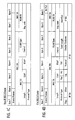
- Figures 4A-4F are diagrams illustrating data packet structures having different protocols that may be received and processed by the network switch of Figure 1.
- Figures 5A and 5B are diagrams illustrating the structures for the register files of Figure 3 for received data packets having alternative addressing protocols, respectively.
- Figure 6 is a block diagram illustrating the instruction control unit of Figure 3.
- Figure 7 is a diagram illustrating in detail an instruction execution control unit fetched from the instruction memory of Figure 3.
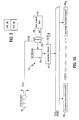
- Figure 1 is a block diagram of a network switch configured for sending and receiving data packets on a high speed network (e.g., 100 Mb/s or 1 Gb/s) according to an embodiment of the present invention. As shown in Figure 1, the
network switch 10 includes aswitch fabric 12 having a plurality of 100 Mb/s or 1 Gb/s network switch ports 14, each configured for sending and receiving data packets according to a media access control (MAC) layer protocol (e.g.. Ethernet, IEEE 802.3), also referred to as a layer-2 protocol, and optionally a network layer protocol. (for example Internet protocol Version 4 (IPv4) or Version 6 (IPv6)), also referred to as a layer-3 protocol. Although Figure 1 shows only fournetwork switch ports - The
network switch 10 also includes switchinglogic 18 for determining the network ports 14 that are to output a data packet received by thenetwork switch 10. According to the disclosed embodiment, the switchinglogic 18 concurrently determines the output network ports for a plurality of received data packets to maintain switching capacity at the wire rate of, for example, 100 Mb/s or 1 Gb/s. As described below, thenetwork switch 10 obtains destination address information for each received data packet from anexternal memory 24. As will be recognized in the art, address learning is first performed by the network switch to populate theexternal memory 24 with network addresses, although address learning may also be performed concurrently with network switching operations once theexternal memory 24 stores a minimum number of network addresses. - The switching
logic 18 includes a parsing anddecision logic 20 for identifying the address information for each received packet, and alookup processor 22 for determining a destination output port 14 for each received data packet based on the corresponding destination information identified by the parsing anddecision logic 20. In particular, the parsing anddecision logic 20 identifies for each received data packet the corresponding MAC-layer (i.e., layer-2) source address (MAC SA) and MAC-layer destination address (MAC DA). The parsing anddecision logic 20 also determines whether the received data packet includes a virtual LAN (VLAN) field according to IEEE 802.1d protocol that provides enhanced addressing capabilities. The parsing anddecision logic 20 also identifies the protocol of the MAC-layer addressing, for example whether the MAC-layer addressing is Ethernet-based or IEEE 802.3-based addressing. - The parsing and
decision logic 20 also detects whether a higher layer (layer-3) network-based addressing protocol is present in the received data packet, for example IPv4 or IPv6. Examples of alternative addressing protocols are shown in Figures 4A-4F. As shown in Figures 4A-4F, the parsing anddecision logic 20 can be configured to identify layer-2 Ethernet-based addressing, as shown in Figures 4A, 4B, and 4E, as well as addressing using IEEE 802.3 addressing protocol, as shown in Figures 4C, 4D, and 4F. In addition, the parsing anddecision logic 20 can be configured for identifying network-based (layer-3) addressing, for example IP-based addressing, as shown in Figures 4A, 4D, 4E, and 4F. - Determination of layer-3 addressing capabilities requires the parsing and
decision logic 20 to interpret the payload of the MAC-layer (layer-2) packet. Hence, the parsing anddecision logic 20 first determines the addressing protocol at the MAC layer. The parsing anddecision logic 20 then interprets the payload of the MAC-layer packet to identify the presence of layer-3 addressing information. If the parsing anddecision logic 20 determines that the MAC-layer frame includes an IP frame, the parsing anddecision logic 20 then determines whether the IP frame is an lPv4 or IPv6 protocol frame. Based on the determination of the type of addressing protocol found in the data packet, the parsing anddecision logic 20 is able to decide the nature of the addressing lookup operations for thelookup processor 22. - The parsing and
decision logic 20, upon identifying the addressing information at the respective addressing protocol layers as shown in Figures 4A-4F, forwards the addressing information to thelookup processor 22. Specifically, the parsing anddecision logic 20 outputs an addressing protocol identifier that identifies at least whether the layer-2 or layer-3 processing is to be performed. Preferably, the addressing protocol identifier specifies the actual addressing protocol to be used, for example Ethernet or IEEE 802.3 for layer-2 processing, and or lPv4, IPv6, etc. for layer-3 addressing, if applicable. Hence, the addressing protocol identifier specifies an addressing protocol to be used for the corresponding received data packet, for example one of the addressing protocols of Figures 4A-4F, enabling enhanced switching functions for data packets having the appropriate addressing protocol. - The
lookup processor 22 uses the parsed addressing information including the addressing protocol identifier to determine which of the output ports 14 will output the received data packet. As described below, thelookup processor 22 concurrently compares the address information received from the parsing anddecision logic 20 with destination address information stored in an external memory 24 (e.g., a synchronous SRAM), for a plurality of received data packets at the same time. For example, thelookup processor 22 identifies a destination output port by accessing theSSRAM 24 based on at least one of the source address and destination address supplied by the parsing anddecision logic 20 for a given addressing protocol. According to the disclosed embodiment, thelookup processor 22 uses the network-based addressing protocol, if available, to determine the network output port. Alternatively, thelookup processor 22 performs the lookup processing using the appropriate MAC-based addressing protocol if no higher layer protocol is available. Hence, thelookup processor 22 uses layer-3 addressing protocol, if available, and layer-2 processing if the data packet does not have layer-3 addressing. - The
external memory 24 stores port vectors identifying a selected group of the output ports 14 for addresses parsed by thedecision logic 20. For example, a given MAC destination address may identify asingle output port 14a, or may identify all theoutput ports lookup processor 22 performs a lookup operation by accessing theSSRAM 24 based on the address information supplied by the parsing anddecision logic 20 to identify a port vector that specifies the destination output ports for the corresponding data packet. It will be recognized in the art that various addressing schemes can be used, for example accessing theSSRAM 24 using the destination address only, or accessing theSSRAM 24 using a direct accessing scheme based on the destination address at the MAC layer or the IP layer, or index-based addressing, where hash functions are used to generate an index of the destination address for accessing theSSRAM 24. - Regardless of the addressing scheme used by the
lookup processor 22, a primary consideration is that thelookup processor 22 be capable of performing a lookup decision relatively quickly for high speed networks, on the order of within 300 nanoseconds. However. memory access tends to be a relatively slow operation in execution of logical operations, since access of a memory requires one clock cycle for addressing the memory, and another clock cycle for reading the data from the address memory location. Depending on the memory architecture, the number of clock cycles for memory access may be even longer. Hence, there is a need for overcoming the "memory bottleneck" of at least two clock cycles per memory access to enable high speed processing for a network switch in a high speed data network. - In addition, layer-3 based addressing for network switches is still under development. Hence, there is a need for a programmable instruction base for use in a network switch that can be changed as layer-3 switching algorithms are developed.
- According to the disclosed embodiment, the
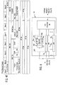
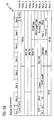
lookup processor 22 provides an architecture that overcomes the two-cycle memory access limitation, effectively reducing the overall access time for accessing theSSRAM 24 from two cycles to one cycle. According to the disclosed embodiment, a pipelining and timesharing approach is used, where multiple lookup operations are concurrently executed in thelookup processor 22 by successively executing the lookup operation within a prescribed number of clock cycles. In particular, thelookup processor 22 concurrently executes such instructions, for example memory read instructions, by successively executing each such instruction within a prescribed number of clock cycles. - Figure 2 is a timing diagram illustrating the arrangement for concurrently determining output switch ports for a prescribed number of data packets by concurrently executing instruction operations during each clock cycle. As shown in Figure 2, the
lookup processor 22 concurrently executes eight instruction operations each 10 nanosecond clock cycle for each fetched instruction. Specifically, Figure 2 illustrates eight instructions (01,02,03,...,08) that are successively fetched during an instruction fetch operation (INST_FETCH) for a prescribed number of execution clock cycles. In particular, each instruction executed by thelookup processor 22 has a corresponding number of instruction operations up to a prescribed number of clock cycles, in this case eight clock cycles. Since each executable instruction has up to eight instruction operations requiring a total of eight clock cycles, thelookup processor 22 is configured for concurrently processing up to eight instructions each clock cycle. Hence, eight concurrent lookup operations are performed by thelookup processor 22 to theSSRAM 24, where each lookup operation for the corresponding instruction is executed in a staggered arrangement relative to the other instructions. - Figure 3 is a block diagram illustrating the
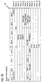
lookup processor 22 according to an embodiment of the present invention. Thelookup processor 22 includes a 3-bit counter 50 for counting a count value each clock cycle of a repeating sequence of a prescribed number of clock cycles. Thecounter 50 is preferably a modulo-8 counter that counts a repeating sequence of eight clock cycles corresponding to the maximum number of execution operations for any instruction. The 3-bit counter 50 outputs a count value that specifies a time slot of the clock cycle, used to enable the logic components of thelookup processor 22 to selectively execute the corresponding instruction operation for selected addresses, described below. - The
lookup processor 22 also includes aninstruction memory 52 having amemory portion 52a for storing a sequence of executable instructions for lookup processing for each of the data packet types shown in Figures 4A-4F. Specifically, theinstruction memory 52a is programmable to enable storage of instructions for performing selected lookup operations according to the addressing protocol identifier, described above, output by the parsing anddecision logic 20. Hence, theinstruction memory 52 has instruction sequences for lookup operations for Ethernet or IEEE 802.3 processing (layer-2) plus Ipv4 or Ipv6 (layer-3) processing. The instruction memory also includes amultiplexer 52b for selectively outputting an instruction address for fetching a selected address from theinstruction memory 52a. Themultiplexer 52b selectively outputs one of a plurality of addresses specifying a different instruction to be executed by thelookup processor 22. - The
lookup processor 22 also includes aninstruction control unit 54 for concurrently supplying the instruction addresses to themultiplexer 52b for execution of the above-described execution sequences for respective data packets according to layer-2 or layer-3 processing. Figure 6 is a diagram illustrating in detail theinstruction control unit 54. Theinstruction control unit 54 includes a plurality of program counter circuits 56 for outputting the instruction address for a corresponding instruction sequence of a lookup operation to be performed. Each program counter circuit 56 supplies an instruction address to themultiplexer 52b (e.g., IA0, IA1, ..., IA7) and includes astart register 56a for storing a start address for the instruction sequence, abranch register 56b for storing a branch address specified by an instruction (e.g., a jump instruction or conditional branch instruction), and a program counter register 56c for storing a current address to be executed. Each program counter circuit 56 also includes amultiplexer 56d for selectively outputting the start address stored in theregister 56a, the branch address stored in theregister 56b, or the program counter address stored in the register 56c based on program instruction control signals. As shown in Figure 6, theinstruction control unit 54 also includes aninstruction controller 58 for generating the program instruction control signals for each of the program counter circuits 56 based on a corresponding instruction sequence (i.e., a code sequence) for performing a prescribed operation, for example a lookup for a MAC-layer protocol or a network-layer protocol. Theinstruction controller 58 generates the program instruction control signals for themultiplexer 56d, and loads the appropriate address values into theregisters instruction controller 58 controls the fetching of a sequence of instructions by loading the start address for the first instruction into thestart address 56a, and controlling themultiplexer 56d to output the start address from theregister 56a. The start address also is loaded from theregister 56a into the program counter 56c, enabling the program count value to be incremented for the next instruction in the instruction sequence. If a branch operation is to be performed, theinstruction controller 58 controls the correspondingmultiplexer 56d to output the value from thebranch register 56b, and loads the branch value into the program counter register 56c. - The
instruction controller 58 generates the program instruction control signals for each of the program counter circuits 56 (LA0...LA7) for execution of a corresponding lookup operation based on an identified addressing protocol for a corresponding received data packet. The instruction controller 28 receives the identified addressing protocol for the corresponding data packet from acorresponding register file 62, described below. - As shown in Figure 3, the
lookup processor 22 further includes aninstruction decoder 60 for decoding, each clock cycle, the instruction fetched from theinstruction memory 52a during a preceding clock cycle. For example, assuming in Figure 2 that theinstruction control unit 54 supplies an instruction address forinstruction 01 duringclock cycle 30 in Figure 2, theinstruction memory 52a performs the instruction operation INST_FETCH of fetching and outputtinginstruction 01 from the addressed memory location during the first relative clock cycle (CCI) occurring atreal clock cycle 30. A "relative clock cycle" refers to a relative position of an instruction operation during execution of a corresponding instruction. Theinstruction decoder 60 decodesinstruction 01 as instruction operation INST_DECODE during the relative clock cycle CC2 atreal clock cycle 32. - Hence, the
instruction decoder 60 decodes a fetched address output from theinstruction memory 52a each clock cycle. For example, Figure 2 illustrates that the decoding operation (INST_DECODE) decodes the first instruction duringclock cycle 32, the second instruction (02) duringclock cycle 34, the third instruction (03) duringclock cycle 36, etc. Hence, theinstruction decoder 60 successively decodes each clock cycle a fetched instruction output from theinstruction memory 52. - The
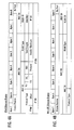
lookup processor 22 also includes a plurality of register files 62 for storing the parsed data supplied from the parsing anddecision logic 20. Each register file stores the parsed data for a corresponding received data packet dunng the lookup processing performed by thelookup processor 22. Hence, thelookup processor 22 has the capacity to simultaneously store the parsed data for eight received data packets in the respective register files 0-7. - Figures 5A and 5B are diagrams illustrating the organization of each
register file 62 for received data packets parsed by the parsing anddecision logic 20. In particular, Figure 5A illustrates the register file organization for a received data packet having IEEE 802.3 layer-2 protocol andlPv4 layer 3 protocol. and Figure 5B illustrates the register file organization for a received data packet having IEEE 802.3 layer-2 protocol and Ipv6 layer-3 protocol. As described above, the layer-2 and layer-3 protocol identifiers are supplied to theinstruction control unit 54 to enable execution of the appropriate instruction sequence for the corresponding layer-2 and layer-3 protocols. As described below, an instruction executed by thelookup processor 22 accesses data from the register file by addressing a corresponding source register 53, shown in Figure 3. - Figure 7 is a diagram illustrating in detail an
instruction 100 decoded by theinstruction decoder 60. As shown in Figure 7, the instruction includes an op code control (OC) that specifies the logical operation to be performed, for example load, read, or add. The destination field (DEST) specifies an address location in a selectedregister file 62 for storing the result of the logical operation specified by the op code field. Source register (SRC Reg.) 1 and source register 2 store address locations of respective operands in thecorresponding register file 62, respectively. The bit mask register specifies an address for a stored mask in a mask register 64 (see Figure 3), if applicable. The memory register (Mem Reg.) stores an address location for direct addressing of theSRAM 24, if applicable. The branch address stores a branch address to be used by theinstruction controller 58, for example if the logical operation provides a prescribed result. - The
lookup processor 22 further includes amemory interface 66 for selectively supplying memory addresses, decoded each clock cycle by theinstruction decoder 60, to theexternal memory 24. Thememory interface 66 includes anaddress register 68, afirst multiplexer 70 for controlling theaddress register 68 based on the corresponding op code control (OC) selected during the corresponding clock sequence, anaddress multiplexer 72 for selectively supplying a memory address location to theaddress register 68 in response to the appropriate clock cycle. Thememory interface 66 also includes adata register 74 for storing data to be written to theSSRAM 24, an op code multiplexer 76 for selectively controlling the data register 74 according to the appropriate clock cycle, and adata multiplexer 78 for selectively supplying data to the data register 74 in accordance with the appropriate relative clock cycle. As shown in Figure 2, address data from the decoded instruction is loaded into theaddress register 68 as instruction operation ERC_ADDR during the relative clock cycle CC3. The memory address stored in theaddress register 68 is then supplied to anSRAM address register 24a as instruction operation S_ADDR during the relative clock cycle CC4. Thesynchronous SRAM 24 then fetches the address data during relative clock cycle CC5 as the instruction operation S_DATA, and stores the fetched data in itsinternal output register 24c. - As shown in Figure 3, the
lookup processor 22 includes a memory data register 80 for latching the data supplied by theSRAM 24 from thedata output register 24c as the instruction operation ERC_DATA during the relative clock cycle CC6. - The
lookup processor 22 also includes an arithmetic logic unit (ALU) 82 that selectively performs arithmetic operations based on op code control signals supplied bymultiplexer 84 and the logical operands selectively supplied from the register files 62 bymultiplexers 86 and 88. TheALU 82 performs the logical operation specified by the op code control (OC*) output by themultiplexer 84, and stores the logical result in a holdingregister 90. The logical result stored in the holdingregister 90 is used to selectively set the flags in aflag register 92. The logical value in the holding register 90 (e.g., summation result from the operation ADD:C←A+B) is output to thedemultiplexer 94 for storage in thecorresponding register file 62 as a write back instruction operation (W_BACK) during relative clock cycle CC8. - As shown in Figure 3, the
multiplexers 88 selectively supply operands to thearithmetic logic Unit 82 during any of the relative clock cycles CC3, CC4, CC5, CC6, or CC7, depending on the logical operation being performed. According to the disclosed embodiment, comparisons between data stored in a selected one of the register files 62 (e.g., layer-2 or layer-3 addressing data) are compared with data fetched from theSSRAM 24 following the external rules checker data retrieval instruction operation during relative clock cycle CC6, during which point data stored in the data register 80 is supplied to themultiplexer 86b. Theregisters multiplexer 84 during relative clock cycle CC7. TheALU 82 performs the logical instruction operation M_CMP_BR during relative clock cycle CC7, and outputs the logical result to the holdingregister 90. The holdingregister 90 outputs the result to thedemultiplexer 94, enabling the result to be written back to theappropriate register file 62 duringclock cycle 8. Each of themultiplexers counter 50 to enable execution of the corresponding instruction operation based on the count value output by thecounter 50 and the corresponding position (CCi) in the execution sequence. - Hence, the
lookup processor 22 is configured for concurrently executing fetched instructions by successively executing each of the fetched instructions within a prescnbed number of clock cycles. For example, thelookup processor 22 executes the instruction operation INST_FETCH forinstruction 01 duringclock cycle 30. The subsequent instruction operations at the relative clock cycles (CC2, CC3, CC4, CC5, CC6, CC7, and CC8) forinstruction 1 are performed during clock cycles 32, 34, 36, 38, 40, 42, and 44, respectively. Conversely, each logic component of the lookup processor 22 (e.g., decoder 60) performs the corresponding instruction operation for the selected instruction during each clock cycle. Hence, theinstruction decoder 60 performs the decoding operation forinstructions lookup processor 22 successively executes the corresponding instruction operation, during each clock cycle, for the corresponding instruction. Consequently, thelookup processor 22 provides the performance of concurrently executing 8 lookup operations, without the necessity of additional redundant logic circuitry as normally found in parallel processing architectures. Hence. the disclosedlookup processor 22 provides the performance of concurrently executing multiple instructions; without the expense normally associated with parallel-processing architectures. - According to the disclosed embodiment, instructions are concurrently executed in a processor within a prescribed number of clock cycles without the necessity of redundant logical components. Since each of the instruction operations are executed independently of each other, the disclosed embodiment enables any type of processor-based instruction operation to be performed in an efficient manner. Hence, the disclosed arrangement is particularly advantageous for systems that require high throughput, yet require a flexible instruction base for applications such as layer-3 addressing operations, that make hardware implementation (e.g., reduction to silicon) an impractical solution. Hence, the disclosed embodiment provides an efficient, flexible and low cost processing architecture for demanding applications such as high speed network switching.
- Although the disclosed processor architecture has been described with respect to lookup operations for network addressing, it will be appreciated that the disclosed embodiment is applicable to other processing applications that require effectively simultaneous execution of multiple instructions.
- While this invention has been described in connection with what is presently considered to be the most practical and preferred embodiments, it is to be understood that the invention is not limited to the disclosed embodiments, but, on the contrary, is intended to cover various modifications and equivalent arrangements included within the spirit and scope of the appended claims.
Claims (26)
- A method of executing instruction operations, comprising:successively fetching instructions during a respective prescribed number of cycles; andconcurrently executing the fetched instructions by successively executing each of the fetched instructions within the prescribed number of cycles.
- The method of claim 1, wherein the successively fetching step comprises:fetching a first of the instructions during a first of the cycles;fetching a second of the instructions during a second of the cycles contiguously following the first cycle; andfetching a third of the instructions during a third of the cycles contiguously following the second cycle.
- The method of claim 2, wherein the successively executing step comprises:initiating execution of the first instruction at the second cycle; andinitiating execution of the second instruction at the third cycle.
- The method of claim 3, wherein the step of initiating execution of the first instruction comprises:decoding the first instruction during the second cycle; andsupplying a memory address to a memory during the third cycle in response to the decoding step.
- The method of claim 4, wherein the step of initiating execution of the first instruction further comprises:causing the memory to latch the supplied memory address during a fourth cycle contiguously following the third cycle;causing the memory to access memory data in response to the supplied memory address during a fifth cycle contiguously following the fourth cycle; andloading the accessed memory data into a data register during a sixth cycle contiguously following the fifth cycle.
- The method of claim 5, wherein the step of initiating execution of the second instruction comprises:decoding the second instruction during the third cycle; andsupplying a second memory address to the memory during the fourth cycle in response to the second instruction decoding step.
- The method of claim 4, wherein the step of initiating execution of the second instruction further comprises:causing the memory to latch the supplied second memory address during the fifth cycle;causing the memory to access second memory data, in response to the supplied second memory address, dunng the sixth cycle; andloading the accessed second memory data into a data register during a seventh cycle contiguously following the sixth cycle.
- A method in a processor circuit of concurrently executing a plurality of instructions, comprising:establishing a prescribed number of clock cycles for executing an executable instruction in the processor circuit, each executable instruction having a corresponding number of instruction operations up to the prescribed number of clock cycles; andconcurrently executing one of the instruction operations for each of the instructions in respective logic components of the processor circuit during each clock cycle.
- The method of claim 8, wherein the establishing step comprises setting a counter to count a repeating sequence of the prescribed number of clock cycles, the counter outputting a count value specifying a time slot of the clock cycles.
- The method of claim 8, wherein the logic components each have corresponding execution sequence positions, the concurrently executing step comprising:selectively offsetting the count value for selected logic components according to a corresponding position in a prescribed execution order; andsupplying to each of the logic components the corresponding count value for selective execution of the corresponding instruction operation for the selected instruction.
- The method of claim 8, wherein the logic components include an instruction memory for storing the instructions and a decoder for decoding an instruction fetched from the instruction memory, the concurrently executing step comprising:selectively supplying to the instruction memory an instruction address identifying a first of the instructions during a first of the clock cycles;decoding in the decoder, during the first clock cycle, a previous instruction fetched from the instruction memory during the clock cycle contiguously preceding the first instruction cycle; anddecoding in the decoder, during a second clock cycle contiguously following the first clock cycle, the first instruction fetched from the instruction memory during the first clock cycle to identify the corresponding instruction operations.
- The method of claim 11, wherein the logic components include a memory interface having an address register and a memory read data register, the concurrently executing step further comprising:executing a first instruction operation for the first instruction that loads a memory address into the address register during a third clock cycle contiguously following the second clock cycle;executing a second instruction operation for the first instruction that causes the memory interface to supply the memory address to a memory during a fourth clock cycle contiguously following the third clock cycle;executing a third instruction operation for the first instruction that causes the memory to access memory data in response to the supplied memory address during a fifth clock cycle contiguously following the fourth clock cycle;executing a fourth instruction operation for the first instruction that causes the memory interface to load the memory data into the memory read data register during a sixth clock cycle contiguously following the fifth clock cycle.
- The method of claim 12, wherein the concurrently executing step further comprises:selectively supplying to the instruction memory an instruction address identifying a second of the instructions during the second clock cycle;decoding in the decoder, during the third clock cycle, the second instruction fetched from the instruction memory during the second instruction cycle to identify the corresponding instruction operations.
- The method of claim 13, wherein the concurrently executing step further comprises:executing a first instruction operation for the second instruction that loads a memory address into the address register during the fourth clock cycle;executing a second instruction operation for the second instruction that causes the memory interface to supply the memory address to the memory during the fifth clock cycle;executing a third instruction operation for the second instruction that causes the memory to access memory data in response to the supplied memory address during the sixth clock cycle;executing a fourth instruction operation for the second instruction that causes the memory interface to load the memory data into the memory read data register during a seventh clock cycle contiguously following the sixth clock cycle.
- The method of claim 14, wherein the logic components include an arithmetic logic unit and a register file configured for storing operands for the fetched instructions, the concurrently executing step further comprising:executing a fifth instruction operation for the first instruction that causes the arithmetic logic unit to perform a selected operation with a selected operand from the register file during the seventh clock cycle; andexecuting a sixth instruction operation for the first instruction that causes storage of a result of the operation by the arithmetic logic unit to be stored in the register file during an eighth clock cycle contiguously following the seventh clock cycle.
- A method in a processor circuit, having logic components, for concurrently executing a plurality of instructions, the method comprising:outputting a count value each clock cycle that identifies one of a prescribed number of clock cycles, each instruction having a corresponding number of instruction operations up to the prescribed number of clock cycles; andselecting based on the count value, by each logic component, one of a plurality of operands associated with a corresponding instruction for execution of a corresponding instruction operation each clock cycle.
- The method of claim 16, wherein each logic component comprises a multiplexer and instruction operation circuitry for performing the corresponding instruction operation, the selecting step for each logic component comprising:receiving by the corresponding multiplexer the operands for execution of the corresponding instruction operation for the respective instructions; andselectively outputting the selected one operand from the multiplexer to the corresponding instruction operation circuitry based on the count value.
- A method in a network switch for determining output switch ports for received data packets, comprising:receiving for each of the received data packets a destination address and an addressing protocol identifier; andconcurrently determining output switch ports for a prescnbed number of data packets, comprising:(1) successively fetching an executable instruction each clock cycle for a corresponding data packet based on the corresponding addressing protocol identifier, the executable instruction having a corresponding prescnbed number of instruction operations up to the prescribed number;(2) concurrently executing, during each clock cycle, one of the instruction operations for each of the fetched instructions for the corresponding data packet, at least one of the instruction operations including comparing a stored address to the destination address to determine the output switch port for the corresponding data packet.
- A processor apparatus, comprising:a counter for outputting a count value, each clock cycle, of a repeating sequence of a prescribed number of clock cycles;an instruction memory for selectively fetching, each clock cycle, one of a plurality of instructions identified by respective instruction addresses supplied during each clock cycle, the instruction memory selecting the corresponding one supplied instruction address based on the count value;an instruction decoder for decoding, each clock cycle, the fetched instruction output from the instruction memory the preceding clock cycle, the instruction decoder configured for identifying a memory address and an instruction operation for each fetched instruction;a memory interface for selectively supplying to an external memory, each clock cycle, one of a plurality of the memory addresses supplied during each clock cycle and identified by the instruction decoder for the respective fetched instructions, the memory interface selecting the corresponding one supplied memory address based on the count value; anda logic unit configured for selectively executing, each clock cycle, one of the instruction operations for the corresponding fetched instruction using memory data retrieved from the supplied memory address, the logic unit selecting the one instruction operation based on the count value.
- The processor apparatus of claim 19, further comprising an instruction control unit for concurrently supplying the instruction addresses to instruction addresses to the instruction memory, the instruction control unit comprising:a plurality of program counter circuits for outputting the instruction addresses, respectively, each program counter circuit including a start register for storing a start address, a branch register for storing a branch address, a program counter register for incrementing the corresponding instruction address, and a multiplexer for selectively outputting one of the start address, the branch address, and the incremented instruction address as the instruction address in response to program instruction control signals; andan instruction controller for generating the program instruction control signals for each of the program counter circuits in response to a corresponding instruction sequence.
- The processor apparatus of claim 19, wherein the instruction memory comprises a first multiplexer receiving the plurality of instructions for the prescribed number of clock cycles, the first multiplexer outputting the one selected instruction address in response to the count value.
- The processor apparatus of claim 21, wherein the memory interface comprises a second multiplexer receiving the supplied memory addresses, the second multiplexer outputting the one supplied memory address in response to the count value and based on a corresponding position of the memory interface in a prescribed execution order.
- A network switch comprising:a plurality of network ports, each configured for sending and receiving data packets selectively according to at least one of a first layer protocol and a second layer protocol. the first layer protocol specifying a first data packet type having a first layer address and a first payload, the second layer protocol specifying a second data packet type having a second layer address and a second payload carrying the first data packet type;switching logic for concurrently determining output network ports for respective received data packets, the switching logic selectively comparing one of the first layer address and the second layer address of each received data packet with a corresponding stored destination address based on identification of one of the first and second layer protocols; andswitch fabric for outputting the received data packets to the determined output network ports.
- The network switch of claim 23, wherein the switching logic comprises:parsing and decision logic for identifying for each received data packet the corresponding second layer address, the parsing and decision logic determining an addressing protocol based on detection of a presence of the first layer address according to the corresponding first layer protocol; anda lookup processor for concurrently comparing one of the first layer addresses and the second layer addresses for the received data packets, based on the determined addressing protocol, with the stored destination addresses.
- The network switch of claim 24, wherein the lookup processor successively accesses, during each clock cycle, one of the stored destination addresses from an external random access memory.
- The network switch of claim 25, wherein the lookup processor includes a plurality of unique logic components, each of the unique logic components executing a corresponding instruction operation for a corresponding selected one of the received data packets each clock cycle.
Applications Claiming Priority (2)
| Application Number | Priority Date | Filing Date | Title |
|---|---|---|---|
| US09/112,146 US6112294A (en) | 1998-07-09 | 1998-07-09 | Concurrent execution of multiple instructions in cyclic counter based logic component operation stages |
| US112146 | 1998-07-09 |
Publications (2)
| Publication Number | Publication Date |
|---|---|
| EP0971289A2 true EP0971289A2 (en) | 2000-01-12 |
| EP0971289A3 EP0971289A3 (en) | 2004-02-25 |
Family
ID=22342333
Family Applications (1)
| Application Number | Title | Priority Date | Filing Date |
|---|---|---|---|
| EP99303069A Withdrawn EP0971289A3 (en) | 1998-07-09 | 1999-04-21 | Apparatus and method for concurrently executing multiple instructions |
Country Status (2)
| Country | Link |
|---|---|
| US (1) | US6112294A (en) |
| EP (1) | EP0971289A3 (en) |
Cited By (1)
| Publication number | Priority date | Publication date | Assignee | Title |
|---|---|---|---|---|
| US20130058319A1 (en) * | 2011-09-02 | 2013-03-07 | Kuo-Yen Fan | Network Processor |
Families Citing this family (11)
| Publication number | Priority date | Publication date | Assignee | Title |
|---|---|---|---|---|
| US6978309B1 (en) * | 2000-07-31 | 2005-12-20 | Cisco Technology, Inc. | Method and system for reprogramming instructions for a switch |
| US6839351B1 (en) * | 2001-03-28 | 2005-01-04 | Advanced Micro Devices, Inc. | Parallel packet lookup in a packet-switched network |
| US7376811B2 (en) * | 2001-11-06 | 2008-05-20 | Netxen, Inc. | Method and apparatus for performing computations and operations on data using data steering |
| US20040128475A1 (en) * | 2002-12-31 | 2004-07-01 | Gad Sheaffer | Widely accessible processor register file and method for use |
| US6996785B1 (en) | 2003-04-25 | 2006-02-07 | Universal Network Machines, Inc . | On-chip packet-based interconnections using repeaters/routers |
| US10990326B2 (en) | 2017-05-31 | 2021-04-27 | Fmad Engineering Kabushiki Gaisha | High-speed replay of captured data packets |
| US11036438B2 (en) | 2017-05-31 | 2021-06-15 | Fmad Engineering Kabushiki Gaisha | Efficient storage architecture for high speed packet capture |
| US11128740B2 (en) * | 2017-05-31 | 2021-09-21 | Fmad Engineering Kabushiki Gaisha | High-speed data packet generator |
| US10423358B1 (en) | 2017-05-31 | 2019-09-24 | FMAD Engineering GK | High-speed data packet capture and storage with playback capabilities |
| US11392317B2 (en) | 2017-05-31 | 2022-07-19 | Fmad Engineering Kabushiki Gaisha | High speed data packet flow processing |
| CN109347474B (en) * | 2018-09-28 | 2022-09-23 | 深圳忆联信息系统有限公司 | Signal time sequence configuration method and device, computer equipment and storage medium |
Citations (3)
| Publication number | Priority date | Publication date | Assignee | Title |
|---|---|---|---|---|
| US4438488A (en) * | 1979-06-26 | 1984-03-20 | Tokyo Shibaura Denki Kabushiki Kaisha | Data processing system with a slave computer using data registers as the sole operand store |
| WO1996037830A1 (en) * | 1995-05-26 | 1996-11-28 | National Semiconductor Corporation | Microprocessor with pipelined access request to external memory |
| US5710914A (en) * | 1995-12-29 | 1998-01-20 | Atmel Corporation | Digital signal processing method and system implementing pipelined read and write operations |
Family Cites Families (6)
| Publication number | Priority date | Publication date | Assignee | Title |
|---|---|---|---|---|
| FR2557712B1 (en) * | 1983-12-30 | 1988-12-09 | Trt Telecom Radio Electr | PROCESSOR FOR PROCESSING DATA BASED ON INSTRUCTIONS FROM A PROGRAM MEMORY |
| JP2682232B2 (en) * | 1990-11-21 | 1997-11-26 | 松下電器産業株式会社 | Floating point processor |
| US5471626A (en) * | 1992-05-06 | 1995-11-28 | International Business Machines Corporation | Variable stage entry/exit instruction pipeline |
| JPH05342084A (en) * | 1992-06-08 | 1993-12-24 | Matsushita Electric Ind Co Ltd | Device and method for storing data |
| US5835968A (en) * | 1996-04-17 | 1998-11-10 | Advanced Micro Devices, Inc. | Apparatus for providing memory and register operands concurrently to functional units |
| US5958045A (en) * | 1997-04-02 | 1999-09-28 | Advanced Micro Devices, Inc. | Start of access instruction configured to indicate an access mode for fetching memory operands in a microprocessor |
-
1998
- 1998-07-09 US US09/112,146 patent/US6112294A/en not_active Expired - Lifetime
-
1999
- 1999-04-21 EP EP99303069A patent/EP0971289A3/en not_active Withdrawn
Patent Citations (3)
| Publication number | Priority date | Publication date | Assignee | Title |
|---|---|---|---|---|
| US4438488A (en) * | 1979-06-26 | 1984-03-20 | Tokyo Shibaura Denki Kabushiki Kaisha | Data processing system with a slave computer using data registers as the sole operand store |
| WO1996037830A1 (en) * | 1995-05-26 | 1996-11-28 | National Semiconductor Corporation | Microprocessor with pipelined access request to external memory |
| US5710914A (en) * | 1995-12-29 | 1998-01-20 | Atmel Corporation | Digital signal processing method and system implementing pipelined read and write operations |
Cited By (2)
| Publication number | Priority date | Publication date | Assignee | Title |
|---|---|---|---|---|
| US20130058319A1 (en) * | 2011-09-02 | 2013-03-07 | Kuo-Yen Fan | Network Processor |
| US9246846B2 (en) * | 2011-09-02 | 2016-01-26 | Mediatek Co. | Network processor |
Also Published As
| Publication number | Publication date |
|---|---|
| EP0971289A3 (en) | 2004-02-25 |
| US6112294A (en) | 2000-08-29 |
Similar Documents
| Publication | Publication Date | Title |
|---|---|---|
| US10764200B2 (en) | Openflow match and action pipeline structure | |
| US5917821A (en) | Look-up engine for packet-based network | |
| US8743877B2 (en) | Header processing engine | |
| US7313667B1 (en) | Methods and apparatus for mapping fields of entries into new values and combining these mapped values into mapped entries for use in lookup operations such as for packet processing | |
| US6308220B1 (en) | Circulating parallel-search engine with random inputs for network routing table stored in a wide embedded DRAM | |
| US7894451B2 (en) | Method of providing virtual router functionality | |
| US6032190A (en) | System and method for processing data packets | |
| US6754211B1 (en) | Method and apparatus for wire speed IP multicast forwarding | |
| US7080238B2 (en) | Non-blocking, multi-context pipelined processor | |
| US7336660B2 (en) | Method and apparatus for processing packets based on information extracted from the packets and context indications such as but not limited to input interface characteristics | |
| US6112294A (en) | Concurrent execution of multiple instructions in cyclic counter based logic component operation stages | |
| US7830892B2 (en) | VLAN translation in a network device | |
| US6721800B1 (en) | System using weighted next hop option in routing table to include probability of routing a packet for providing equal cost multipath forwarding packets | |
| WO1996034479A1 (en) | Packet switching engine | |
| US6920562B1 (en) | Tightly coupled software protocol decode with hardware data encryption | |
| US6625146B1 (en) | Method and apparatus for operating a network switch in a CPU-less environment | |
| US10944696B2 (en) | Variable-length packet header vectors | |
| US20030159021A1 (en) | Selected register decode values for pipeline stage register addressing | |
| US6697380B1 (en) | Multiple key lookup arrangement for a shared switching logic address table in a network switch | |
| US6778547B1 (en) | Method and apparatus for improving throughput of a rules checker logic | |
| US20040246956A1 (en) | Parallel packet receiving, routing and forwarding | |
| US7065083B1 (en) | Method and apparatus for dynamically generating lookup words for content-addressable memories | |
| EP1631906B1 (en) | Maintaining entity order with gate managers | |
| US6684300B1 (en) | Extended double word accesses | |
| US7327722B1 (en) | Bridging routed encapsulation |
Legal Events
| Date | Code | Title | Description |
|---|---|---|---|
| PUAI | Public reference made under article 153(3) epc to a published international application that has entered the european phase |
Free format text: ORIGINAL CODE: 0009012 |
|
| AK | Designated contracting states |
Kind code of ref document: A2 Designated state(s): AT BE CH CY DE DK ES FI FR GB GR IE IT LI LU MC NL PT SE |
|
| AX | Request for extension of the european patent |
Free format text: AL;LT;LV;MK;RO;SI |
|
| RIC1 | Information provided on ipc code assigned before grant |
Ipc: 7G 06F 9/32 B Ipc: 7G 06F 9/38 A |
|
| PUAL | Search report despatched |
Free format text: ORIGINAL CODE: 0009013 |
|
| AK | Designated contracting states |
Kind code of ref document: A3 Designated state(s): AT BE CH CY DE DK ES FI FR GB GR IE IT LI LU MC NL PT SE |
|
| AX | Request for extension of the european patent |
Extension state: AL LT LV MK RO SI |
|
| 17P | Request for examination filed |
Effective date: 20040726 |
|
| AKX | Designation fees paid |
Designated state(s): DE GB |
|
| RBV | Designated contracting states (corrected) |
Designated state(s): DE FR GB |
|
| 17Q | First examination report despatched |
Effective date: 20050223 |
|
| RAP1 | Party data changed (applicant data changed or rights of an application transferred) |
Owner name: GLOBALFOUNDRIES, INC. |
|
| STAA | Information on the status of an ep patent application or granted ep patent |
Free format text: STATUS: THE APPLICATION IS DEEMED TO BE WITHDRAWN |
|
| 18D | Application deemed to be withdrawn |
Effective date: 20111103 |