EP0875852A2 - Smart card - Google Patents
Smart card Download PDFInfo
- Publication number
- EP0875852A2 EP0875852A2 EP98107337A EP98107337A EP0875852A2 EP 0875852 A2 EP0875852 A2 EP 0875852A2 EP 98107337 A EP98107337 A EP 98107337A EP 98107337 A EP98107337 A EP 98107337A EP 0875852 A2 EP0875852 A2 EP 0875852A2
- Authority
- EP
- European Patent Office
- Prior art keywords
- flash memory
- memory
- program
- data
- chip card
- Prior art date
- Legal status (The legal status is an assumption and is not a legal conclusion. Google has not performed a legal analysis and makes no representation as to the accuracy of the status listed.)
- Withdrawn
Links
Images
Classifications
-
- G—PHYSICS
- G06—COMPUTING; CALCULATING OR COUNTING
- G06K—GRAPHICAL DATA READING; PRESENTATION OF DATA; RECORD CARRIERS; HANDLING RECORD CARRIERS
- G06K19/00—Record carriers for use with machines and with at least a part designed to carry digital markings
- G06K19/06—Record carriers for use with machines and with at least a part designed to carry digital markings characterised by the kind of the digital marking, e.g. shape, nature, code
- G06K19/067—Record carriers with conductive marks, printed circuits or semiconductor circuit elements, e.g. credit or identity cards also with resonating or responding marks without active components
- G06K19/07—Record carriers with conductive marks, printed circuits or semiconductor circuit elements, e.g. credit or identity cards also with resonating or responding marks without active components with integrated circuit chips
Abstract
Description
Durch den Einsatz von Mikrocontrollern in integrierten Schaltungen für Chipkarten kann die Sicherheit der in der Karte gespeicherten oder durch die Karte zu verarbeitenden Daten wesentlich erhöht werden. Die Mikrocontrollerschaltung arbeitet ein zumindest teilweise in der Karte gespeichertes Programm (z.B. Betriebssystem und Anwenderprogramme) ab. Zur nicht-flüchtigen Speicherung dieses Programmes wurden bisher ROM-und EEPROM-Schaltungen eingesetzt (siehe zB. Produktschrift der Fa. Philips "ICs for Chip Cards, 07/96)By using microcontrollers in integrated circuits for smart cards, the security of the card data stored or processed by the card be significantly increased. The microcontroller circuit works a program stored at least partially in the card (e.g. operating system and user programs). For Non-volatile storage of this program has so far been used ROM and EEPROM circuits are used (see e.g. product brochure from Philips "ICs for Chip Cards, 07/96)
ROM-Schaltungen haben den Nachteil, daß die Daten während der Fertigung durch einen Maskenschritt festgelegt werden und nachträglich nicht mehr an neue Anforderungen angepasst werden können. Neben der Unveränderlichkeit der Daten weist dieses Verfahren einen weiteren Nachteil auf: Die Daten müssen schon sehr früh vor dem Liefertermin der Karte verfügbar sein. Damit wird die Reaktionszeit und Time to Market deutlich reduziert.ROM circuits have the disadvantage that the data during the Manufacturing can be determined by a mask step and cannot be subsequently adapted to new requirements can. In addition to the immutability of the data, this points Procedure another disadvantage: the data must available very early before the card is due for delivery be. This makes the response time and time to market clear reduced.
EEPROM-Schaltungen können zwar wieder gelöscht und mit neuen Daten beschrieben werden. Sie haben jedoch den Nachteil eines großen Flächenbedarfs und damit hoher Chipkosten.EEPROM circuits can be deleted and replaced with new ones Data are described. However, they have the disadvantage of one large space requirement and thus high chip costs.
Die Aufgabe vorliegende Erfindung ist es daher, eine Chipkarte mit Mikrocontrollerschaltung anzugeben, die diese Nachteile vermeidet.The object of the present invention is therefore a chip card to indicate with microcontroller circuit that these disadvantages avoids.
Die Aufgabe wird dadurch gelöst, daß die Mikrocontrollerschaltung einen Flash-Speicher als Programmspeicher aufweist Vorteilhafte Weiterbildungen der Erfindung ergeben sich aus den Unteransprüchen. The object is achieved in that the microcontroller circuit has a flash memory as program memory Advantageous developments of the invention result from the subclaims.
Die Erfindung beschreibt die Einführung eines Flash-Speichers als Programmspeicher, der bei kleiner Fläche und damit kostengünstiger Herstellung die mehrfache Änderung der Daten nach Abschluß des Herstellprozesses erlaubt. Weiterhin wird der Einsatz einer derartigen Chipkarte für multifunktionale Anwendungen beschrieben.The invention describes the introduction of a flash memory as a program memory that is small in size and therefore less expensive Making multiple changes to the data allowed after completion of the manufacturing process. Will continue the use of such a chip card for multifunctional Applications described.
Die Erfindung wird nachfolgend anhand von Ausführungsbeispielen mit Hilfe von Figuren näher erläutert. Dabei zeigen
- Figur 1
- ein Blockschaltbild einer ersten erfindungsgemäßen Mikrocontrollerschaltung und
- Figur 2
- ein Blockschaltbild einer zweiten erweiterten Ausführung.
- Figure 1
- a block diagram of a first microcontroller circuit according to the invention and
- Figure 2
- a block diagram of a second extended embodiment.
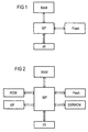
In Fig.1 ist das Blockschaltbild eines erfindungsgemäßen Mikrocontrollerschaltungs für Chipkarten dargestellt. Ein Mikroprozessor MP ist mit einem Flash-Speicher FS als Programmspeicher verbunden. Die Schaltung enthält kein ROM. Der Flash-Speicher ist in besonders vorteilhafter Weise ein Flash-Speicher mit Programmierung durch den Fowler-Nordheim-Effekt. Bei dieser Art der Programmierung wird im Gegensatz zur Programmierung mit dem Hot-Electron-Effekt sehr wenig Strom verbraucht, was eine leistungssparende Schaltung ermöglicht. Ebenso ist die Gefahr der Ausspähung von Daten durch Messung der Stromaufnahme weitgehend ausgeschlossen.1 shows the block diagram of a microcontroller circuit according to the invention shown for chip cards. A microprocessor MP is with a flash memory FS as program memory connected. The circuit does not contain ROM. Of the Flash memory is a particularly advantageous one Flash memory with programming through the Fowler-Nordheim effect. This type of programming is opposed very little for programming with the hot electron effect Consumes electricity, which enables a power-saving circuit. Likewise, there is a risk of spying on data Measurement of current consumption largely excluded.
Weiterhin vorteilhaft ist der Einsatz eines Flash-Speichers mit negativer Programmierspannung auf dem Controlgate wie er in der Druckschrift "A 0.5µm CMOS Technology for Multifunctional Applications with Embedded FN-Flash Memory and Linear R and C Modules" von R. Heinrich, W. Heinrigs, G. Tempel, J. Winnerl, T. Zettler, in Proc. of the International Electron Devices Meeting (IEDM) 1993, p. 445-448 beschrieben wird. Bei einem derartigen Speicher kann die positive Spannung im Draingebiet der Speicherzellen auf kleine Werte (z. B. 5V) begrenzt werden, was die Miniaturisierung der Schaltung erlaubt. Das wiederum ergibt einen Kostenvorteil.The use of a flash memory is also advantageous with negative programming voltage on the Controlgate like him in the publication "A 0.5µm CMOS Technology for Multifunctional Applications with Embedded FN Flash Memory and Linear R and C Modules "by R. Heinrich, W. Heinrigs, G. Tempel, J. Winnerl, T. Zettler, in Proc. of the international Electron Devices Meeting (IEDM) 1993, p. 445-448 becomes. With such a memory, the positive voltage in the drain area of the memory cells to small values (e.g. B. 5V) are limited, which miniaturization of the circuit allowed. This in turn gives a cost advantage.
Der Doppelpfeil in Fig. 1 deutet die wechselseitige Übertragung von Daten und Steuersignalen zwischen dem Mikroprozessor MP und dem Flash-Speicher an. Der Flash-Speicher kann in dieser Konfiguration auch zur Zwischenspeicherung von Daten genutzt werden. Hier ist zu beachten, daß die zwischenzuspeichernden Daten in einem anderen Block als die Programme abgelegt werden müssen, da vor jeder Schreiboperation ein Gesamtlöschen des Blocks erfolgen muß. Die Controllerschaltung verfügt weiterhin über ein RAM zur schnellen flüchtigen Speicherung von Daten. Der als I/0 bezeichnete Input/Output-Block steht entweder für Pad-Eingabe und Ausgabeschaltungen (z. B. serielle Schnittstelle und Pad-Treiber) oder für drahtlose Ein und Ausgabeschaltungen (z.B. RF-Datenübermittlung)The double arrow in Fig. 1 indicates the mutual transmission of data and control signals between the microprocessor MP and the flash memory. The flash memory can be in this Configuration also used for the temporary storage of data will. It should be noted here that the data to be buffered Data stored in a different block than the programs must be erased, since a complete erase before each write operation of the block must be done. The controller circuit has still via RAM for fast volatile storage of data. The input / output block called I / 0 stands for either pad input and output circuits (e.g. serial interface and pad driver) or for wireless Input and output circuits (e.g. RF data transmission)
In Fig. 2 ist eine stark erweiterte Ausführung der Erfindung dargestellt. Die Schaltung enthält wie bereits bei Fig. 1 beschrieben einen Mikroprozessor MP, einen Flash-Speicher FS, ein RAM und eine I/0 Schaltung.2 is a greatly expanded embodiment of the invention shown. The circuit contains as already described in FIG. 1 a microprocessor MP, a flash memory FS, a RAM and an I / 0 circuit.
Im Gegensatz zu Fig. 1 ist hier jedoch zusätzlich ein ROM vorhanden. Dieses ROM kann Programmdaten speichern, welche niemals oder nur sehr selten geändert werden müssen, wie z.B. Basisroutinen. Die Chipkarte arbeitet somit teilweise mit Programmdaten aus dem ROM und teilweise mit Programmen aus dem Flash-Speicher.In contrast to FIG. 1, however, there is also a ROM here available. This ROM can store program data which never or very rarely need to be changed, e.g. Basic routines. The chip card thus works in part Program data from the ROM and partly with programs the flash memory.
Weitere Bestandteile der Schaltung sind ein EEPROM und ein Kryptokoprozessor KP. Das EEPROM kann zur nichtflüchtigen Zwischenspeicherung von Berechnungsdaten genutzt werden. Durch die Programmier- und Löschbarkeit in kleinen Einheiten (z. B. Byteweise) ist dieser Vorgang im EEPROM effizienter als im Flash. Der Kryptokoprozessor dient der Verschlüsselung und Entschlüsselung von Daten für Hochsicherheitsanwendungen. Der Prozessor kann hierfür z.B. einen asymmetrischen Verschlüsselungsalgorhitmus ausführen. Der Koprozessor KP ermöglicht durch seine besondere Struktur die Ausführung der Berechnung in einer wesentlich kürzeren Zeit als dies mittels des normalen Prozessors möglich wäre.Other components of the circuit are an EEPROM and a Cryptocoprocessor KP. The EEPROM can be used for non-volatile Temporary storage of calculation data can be used. Because it can be programmed and deleted in small units (e.g. byte by byte) this process is more efficient in the EEPROM than in flash. The cryptocoprocessor is used for encryption and decryption of data for high security applications. The processor can e.g. an asymmetrical encryption algorithm To run. The coprocessor KP enables due to its special structure, the execution of the calculation in a much shorter time than this of the normal processor would be possible.
Der Einsatz eines Flash-Programmspeichers erlaubt wie bereits erwähnt die nachträgliche Modifikation der Programme. Das ermöglicht die multifunktionale Nutzung der Chipkarte. So kann z.B. beim Ausgabezeitpunkt der Karte ein Teil des Flash-Speichers mit einem Anwenderprogramm belegt werden. Dieses Anwenderprogramm kann durch einen Lösch- und Neuprogrammierschritt durch ein anderes Programm oder z.B. eine neue Version der bestehenden Software ersetzt werden. Weiterhin können ein oder mehrere weitere Anwenderprogramme hinzugeladen werden. Liegen diese Programme im gleichen Löschblock wie das erste Programm, so muß auch das erste Programm neu nachgeladen werden. Liegen die neuen Programme in anderen Blöcken des Flash-Speichers, so bleibt das erste Programm unverändert bestehen.As before, the use of a flash program memory allows mentions the subsequent modification of the programs. This allows the multifunctional use of the chip card. So can e.g. part of the flash memory at the time the card is issued can be assigned with a user program. This User program can be deleted and reprogrammed through another program or e.g. a new version existing software will be replaced. Can continue one or more other user programs can be loaded. Are these programs in the same erase block as that? first program, the first program must also be reloaded will. Are the new programs in other blocks of the Flash memory, the first program remains unchanged.
Die wesentlichen Vorteile der Erfindung bestehen in hoher Flexibilität, schneller Reaktionszeit (Time to Market) und geringer Chipfläche, wodurch solche Mikrocontroller kostengünstiger sind.The main advantages of the invention are high Flexibility, fast response time (time to market) and small chip area, making such microcontrollers less expensive are.
Claims (4)
dadurch gekenzeichnet,
daß die Mikrocontrollerschaltung einen Flash-Speicher (FS) als Programmspeicher aufweist.Chip card with a semiconductor chip having a microcontroller circuit,
characterized by
that the microcontroller circuit has a flash memory (FS) as program memory.
dadurch gekennzeichnet,
daß die Mikrocontrollerschaltung zusätzlich ein ROM als Programmspeicher aufweist.Chip card according to claim 1,
characterized,
that the microcontroller circuit additionally has a ROM as program memory.
dadurch gekennzeichnet,
daß der Flash-Speicher mittels des Fowler-Nordheim-Effekts programmier- und löschbar ist.Chip card according to one of claims 1 or 2,
characterized,
that the flash memory can be programmed and erased using the Fowler-Nordheim effect.
dadurch gekennzeichnet,
daß der Flash-Speicher mittels negativer Programmierspannung am Controlgate einer Flash-Speicherzelle programmierbar ist.Chip card according to one of claims 1 to 3,
characterized,
that the flash memory is programmable using a negative programming voltage on the control gate of a flash memory cell.
Applications Claiming Priority (2)
| Application Number | Priority Date | Filing Date | Title |
|---|---|---|---|
| DE19718446 | 1997-04-30 | ||
| DE1997118446 DE19718446A1 (en) | 1997-04-30 | 1997-04-30 | Chip card with microcontroller circuit |
Publications (2)
| Publication Number | Publication Date |
|---|---|
| EP0875852A2 true EP0875852A2 (en) | 1998-11-04 |
| EP0875852A3 EP0875852A3 (en) | 2002-03-27 |
Family
ID=7828332
Family Applications (1)
| Application Number | Title | Priority Date | Filing Date |
|---|---|---|---|
| EP98107337A Withdrawn EP0875852A3 (en) | 1997-04-30 | 1998-04-22 | Smart card |
Country Status (2)
| Country | Link |
|---|---|
| EP (1) | EP0875852A3 (en) |
| DE (1) | DE19718446A1 (en) |
Families Citing this family (1)
| Publication number | Priority date | Publication date | Assignee | Title |
|---|---|---|---|---|
| DE19956137A1 (en) * | 1999-11-23 | 2001-05-31 | Bundesdruckerei Gmbh | Bearer card, especially personalized identification card, has replaceable module(s), into/from which any information can be written/read, fixed master chip that interacts with modules |
Citations (3)
| Publication number | Priority date | Publication date | Assignee | Title |
|---|---|---|---|---|
| FR2681165A1 (en) * | 1991-09-05 | 1993-03-12 | Gemplus Card Int | Process for transmitting confidential information between two chip cards |
| JPH05120501A (en) * | 1991-10-24 | 1993-05-18 | Mitsubishi Electric Corp | Ic card and manufacturing for the same |
| US5542081A (en) * | 1990-10-02 | 1996-07-30 | Gemplus Card International | IC card designed to receive multiple programs in a progammable memory |
Family Cites Families (1)
| Publication number | Priority date | Publication date | Assignee | Title |
|---|---|---|---|---|
| JPH07302492A (en) * | 1994-05-04 | 1995-11-14 | Internatl Business Mach Corp <Ibm> | Reprogrammable pulg-in cartridge |
-
1997
- 1997-04-30 DE DE1997118446 patent/DE19718446A1/en not_active Ceased
-
1998
- 1998-04-22 EP EP98107337A patent/EP0875852A3/en not_active Withdrawn
Patent Citations (3)
| Publication number | Priority date | Publication date | Assignee | Title |
|---|---|---|---|---|
| US5542081A (en) * | 1990-10-02 | 1996-07-30 | Gemplus Card International | IC card designed to receive multiple programs in a progammable memory |
| FR2681165A1 (en) * | 1991-09-05 | 1993-03-12 | Gemplus Card Int | Process for transmitting confidential information between two chip cards |
| JPH05120501A (en) * | 1991-10-24 | 1993-05-18 | Mitsubishi Electric Corp | Ic card and manufacturing for the same |
Non-Patent Citations (2)
| Title |
|---|
| HEINRICH R ET AL: "A 0.5 /spl mu/m CMOS technology for multifunctional applications with embedded FN-flash memory and linear R and C modules" ELECTRON DEVICES MEETING, 1993. TECHNICAL DIGEST., INTERNATIONAL WASHINGTON, DC, USA 5-8 DEC. 1993, NEW YORK, NY, USA,IEEE, 5. Dezember 1993 (1993-12-05), Seiten 445-448, XP010118346 ISBN: 0-7803-1450-6 * |
| PATENT ABSTRACTS OF JAPAN vol. 017, no. 491 (P-1607), 6. September 1993 (1993-09-06) & JP 05 120501 A (MITSUBISHI ELECTRIC CORP), 18. Mai 1993 (1993-05-18) * |
Also Published As
| Publication number | Publication date |
|---|---|
| DE19718446A1 (en) | 1998-11-19 |
| EP0875852A3 (en) | 2002-03-27 |
Similar Documents
| Publication | Publication Date | Title |
|---|---|---|
| DE69433320T2 (en) | REMOTE CONTROLLED REPROGRAMMABLE PROGRAM MEMORY FOR A MICRO CONTROLLER | |
| DE3622514C2 (en) | ||
| EP0195885B1 (en) | Method and device for the non-volatile memorizing of the counting state of an electronic counter circuit | |
| EP0766211A2 (en) | Multifunctional IC-card | |
| DE4114410A1 (en) | SEMICONDUCTOR COMPONENT WITH NON-VOLATILE STORAGE | |
| WO2000070620A1 (en) | Memory array with address scrambling | |
| DE102006030888A1 (en) | Method and apparatus for generating a starting value for a pseudorandom number generator | |
| EP0875852A2 (en) | Smart card | |
| DE4302553A1 (en) | High security binary counting method for chip card - offsetting final state of binary number w.r.t. sequence such that contents of counter never represents number smaller than previous value | |
| DE10040241A1 (en) | Memory arrangement for portable data carrier e.g. chip card, updates information following deactivation process in such way, that referenced memory areas cover joined memory area | |
| DE10085097B4 (en) | Method and apparatus for controlling compensated buffers | |
| WO2006087192A1 (en) | Method for personalizing a portable data carrier | |
| DE4220877C2 (en) | Methods for non-volatile, erasable and programmable memory devices | |
| EP1308842B1 (en) | Method and device for the management of a memory device | |
| WO2004042740A1 (en) | Method for operating a memory arrangement | |
| EP0404986B1 (en) | Identification circuit for integrated semiconductor circuits | |
| DE10328238B4 (en) | Method for loading smart cards with initialization and / or personalization data | |
| EP0678915A2 (en) | Integrated semiconductor device with an EEPROM, semiconductor substrate with such integrated circuits and method for use of such a semiconductor substrate | |
| WO2004105042A1 (en) | Device and method for treating a state of a memory | |
| EP1008178B1 (en) | Method of producing a read-only memory | |
| EP1517333B1 (en) | Flag for memory with asymmetry concerning programming and erasure | |
| EP1380907A1 (en) | Electronic device for a field device | |
| EP1262998A1 (en) | Voltage pump circuit and application therefor | |
| DE10128752A1 (en) | Storage of data in computer memory, especially EEPROM or flash memory by writing data to memory in pages, whereby each page contains a value and a reference to the next page in the chain | |
| EP1018119B1 (en) | METHOD TO BE APPLIED WHEN EEPROMs ARE USED AS PROGRAMME MEMORIES |
Legal Events
| Date | Code | Title | Description |
|---|---|---|---|
| PUAI | Public reference made under article 153(3) epc to a published international application that has entered the european phase |
Free format text: ORIGINAL CODE: 0009012 |
|
| AK | Designated contracting states |
Kind code of ref document: A2 Designated state(s): AT BE CH CY DE DK ES FI FR GB GR IE IT LI LU MC NL PT SE Kind code of ref document: A2 Designated state(s): AT CH DE ES FR GB IT LI |
|
| AX | Request for extension of the european patent |
Free format text: AL;LT;LV;MK;RO;SI |
|
| RAP1 | Party data changed (applicant data changed or rights of an application transferred) |
Owner name: INFINEON TECHNOLOGIES AG |
|
| PUAL | Search report despatched |
Free format text: ORIGINAL CODE: 0009013 |
|
| AK | Designated contracting states |
Kind code of ref document: A3 Designated state(s): AT BE CH CY DE DK ES FI FR GB GR IE IT LI LU MC NL PT SE |
|
| AX | Request for extension of the european patent |
Free format text: AL;LT;LV;MK;RO;SI |
|
| 17P | Request for examination filed |
Effective date: 20020927 |
|
| AKX | Designation fees paid |
Free format text: AT CH DE ES FR GB IT LI |
|
| 17Q | First examination report despatched |
Effective date: 20030428 |
|
| STAA | Information on the status of an ep patent application or granted ep patent |
Free format text: STATUS: THE APPLICATION IS DEEMED TO BE WITHDRAWN |
|
| 18D | Application deemed to be withdrawn |
Effective date: 20081101 |