EP1517333B1 - Flag for memory with asymmetry concerning programming and erasure - Google Patents
Flag for memory with asymmetry concerning programming and erasure Download PDFInfo
- Publication number
- EP1517333B1 EP1517333B1 EP04018551A EP04018551A EP1517333B1 EP 1517333 B1 EP1517333 B1 EP 1517333B1 EP 04018551 A EP04018551 A EP 04018551A EP 04018551 A EP04018551 A EP 04018551A EP 1517333 B1 EP1517333 B1 EP 1517333B1
- Authority
- EP
- European Patent Office
- Prior art keywords
- state
- memory
- identifier
- flag
- value
- Prior art date
- Legal status (The legal status is an assumption and is not a legal conclusion. Google has not performed a legal analysis and makes no representation as to the accuracy of the status listed.)
- Not-in-force
Links
Images

Classifications
-
- G—PHYSICS
- G11—INFORMATION STORAGE
- G11C—STATIC STORES
- G11C16/00—Erasable programmable read-only memories
- G11C16/02—Erasable programmable read-only memories electrically programmable
- G11C16/06—Auxiliary circuits, e.g. for writing into memory
- G11C16/10—Programming or data input circuits
- G11C16/14—Circuits for erasing electrically, e.g. erase voltage switching circuits
- G11C16/16—Circuits for erasing electrically, e.g. erase voltage switching circuits for erasing blocks, e.g. arrays, words, groups
-
- G—PHYSICS
- G11—INFORMATION STORAGE
- G11C—STATIC STORES
- G11C16/00—Erasable programmable read-only memories
- G11C16/02—Erasable programmable read-only memories electrically programmable
- G11C16/06—Auxiliary circuits, e.g. for writing into memory
- G11C16/10—Programming or data input circuits
Definitions
- the invention relates to a memory device having an asymmetrical electronic memory having a plurality of memory cells with at least one state flag implemented in the memory, which optionally has a first (set, valid) state value or a second (unset, invalid) state value, and that is switchable between the first and the second state value.
- An electronic memory is usually divided into a plurality of memory cells.
- the individual memory cells are brought from a first memory state, for example a logical "1", to a second memory state, for example a logical "0", and vice versa, for which erasures and writes are performed.
- Which state of the deleted and the described memory state while a logical "1" and which is a logical "0" is usually arbitrary and is usually already determined by the manufacturer of the memory.
- a plurality of electronic memories are asymmetric in writing and erasing data, for example, by making the time required for erasing the memory (erasing time or erasing time) different from the amount of time required to write to the memory (write time or write duration).
- the power consumption during writing may be different from the power consumption when deleting.
- the programming voltage to be applied for programming is different, depending on whether the memory is written or deleted.
- the programming voltage here is to be understood as meaning the voltage actually applied to the memory cell which may be different from an external voltage generated by a voltage source which is used to generate the programming voltage.
- a state flag or equivalent flag For example, depending on the state value (flag value), writing (or reading) in the memory section may be either prohibited or allowed.
- the subject matter of the invention is a status code or flag in this sense, that is to say a code by which a status is indicated.
- flags are often used in so-called atomic writes, which are characterized by being either only complete or not at all.
- An example of such an atomic write operation is the writing of data into a smart card, for example, to update an erroneous counter or to charge an electronic purse with a payment ( Rankl, Effing, Handbuch der Chip Actually, 4th edition, Carl Hanser Verlag Kunststoff Vienna, 2002, chapter 5.10 "Atomic Processes", pp. 293-295 ). If new data is to be written into a memory section of the chip card, first the original data, which are stored in the memory section before writing, is copied into a non-volatile buffer memory of the chip card (eg into an EEPROM memory of the chip card).
- the state flag or flag has a valid state value in this case.
- the new data for example, new amount of money in the electronic purse that is equal to the originally existing amount of money reduced by the amount to be paid
- the status flag (flag ) be used to restore the memory contents of the memory portion of the smart card when needed. If the state flag of the buffer memory is set, ie "set to valid", the data from the buffer memory, ie the original data, is written back into the memory section, since previously the new data has not yet been completely programmed in. The new data must be re-registered. In the case of an electronic wallet, therefore, the amount of money that was there before the partially failed debit process (reduction of the amount of money) there was restored in the electronic purse. The load must be repeated.
- State flags are also used in a variety of other different operations except for atomic writes and reads.
- a conventional state flag consists of a single memory cell, e.g. a single bit set to zero "0" or one "1" depending on whether the state flag state flag is valid (flag set) or invalid (flag not set).
- the memory cells contain a material that can assume an amorphous and a crystalline state, one of which corresponds to the described and the other to the erased state. Because switching the material from the amorphous to the crystalline state takes different amounts of time than vice versa, the memory is asymmetrical with respect to writes and erasures.
- a memory device according to the preamble of claims 1 and 16 is known from US 5996041 known.
- the object of the invention is to provide a memory device of the type mentioned, which allows a more efficient switching of the state flag, and to provide a corresponding identification method using a state flag.
- the memory device according to the invention according to the independent claim 1, or the inventive method according to independent claim 16, has, or refers to an electronic memory having a plurality of binary memory cells.
- Each memory cell is switchable by a programming operation between an erased and a written state, wherein by an erase operation, the erased state can be produced and by a write operation of the described state can be produced.
- the memory is asymmetric with respect to writes and erasures, which means in more detail that one or more program parameters have a different (different) value in a write operation than in an erase operation.
- the programming parameters may include: the programming duration, ie the time required to perform a complete programming operation, in particular writing or erasing; the programming voltage, ie the voltage that has to be applied to the memory, in particular to each individual memory cell, in order to carry out a programming operation.
- the memory is further implemented with at least one state flag which may optionally have a first (set, valid) state value or a second (deleted, invalid, not set) state value.
- the memory device has a switching device with which the value of the state identifier can be switched between the first and the second state value, at least one programming process being performed on at least one memory cell for switching the state value.
- the switching means with which the value of the state flag can be switched ie selectively set and cleared, is implemented such that the same type of programming operation for switching from the first to the second state value and to the switching from the second to the first state value Write or delete operation is performed.
- a write operation is performed on a memory cell.
- an erase operation is performed on a memory cell.
- the memory device has the advantage that the state flag (flag) is symmetrical with respect to its setting and erasing. That In particular, the one or more programming parameters such as program duration and / or program voltage have the same value when cleared and set. As a result, no case discrimination needs to be made on whether the flag is set or cleared, so that a switch can be used with a simple structure. The switching of the state flag is thereby more efficient than in known memory devices.
- a memory device which enables a more efficient switching of the state flag.
- precisely one programming operation is carried out on exactly one memory cell for setting and for deleting the status code (flag).
- the memory may be, for example, an EEPROM or a Flash EEPROM (Flash ROM), which is asymmetric in the above sense.
- the components of the memory device according to the invention can be implemented in software form, in hardware form or partly in software form, partly in hardware form.
- the state identifier and the switching device and possibly other components are implemented in software form.
- the asymmetry with respect to write operations and deletions comprises, according to an embodiment of the invention, a write operation of a has a shorter programming time (shorter) than a deletion or vice versa.
- the switching means for switching between the first and second state values of the flag (Flag) uses the programming operation of the writing operation and the erasing operation having a shorter programming period.
- This preferred embodiment has the further advantage that the state flag only uses "fast" programming operations to switch its state value. As a result, the state indicator is particularly time-saving and therefore efficient.
- the asymmetry of writes and erasures involves a write requiring a different (higher or lower) program voltage than an erase.
- a different program voltage Preferably, when switching the state flag that programming operation is used which requires the lower programming voltage.
- This preferred embodiment has the further advantage that the state flag is particularly energy-saving when switching its state value.
- the memory device further has a reset device, with which an output state of the state flag is adjustable.
- a reset device Starting from the initial state, at least one switching operation for switching, in particular setting or clearing, of the state flag (flag) is possible.
- a plurality of successive switching operations is possible starting from the initial state in which the state value of the state flag alternately between valid and invalid, ie alternately always from invalid to valid and once from valid to invalid is switched. In doing so, According to the invention, the same type of programming operation is used for switching, regardless of whether the state flag is switched to valid or to invalid.
- the reset means is also preferably implemented to use the other programming operation of the write and erase operations to set the output state than is used to switch between the first and second state values of the flag.
- a write operation to a memory cell is used to switch the state flag (Flag) and an erase operation is used to set the output state by means of the reset device or vice versa.
- the faster programming operation is used, in which the programming time is lower, whereas for setting the initial state by means of the reset means the slower programming operation is used, in which the programming time is higher.
- the slow programming operation is applied exclusively to the reset, which is usually performed less frequently than the switching of the state flag. In the usually more frequent switching of the state flag, i. when setting and deleting, the fast programming process is used.
- the state flag (Flag) of the power-saving programming process is used, in which a lower programming voltage must be applied to the memory cell (s), whereas to set the output state by means of the reset means the more current-intensive programming operation is used, in which a higher programming voltage must be applied to the memory cell (s).
- the power-intensive programming operation is only in the rare reset the state flag (flag) in use, when switching (set, clear) of the state flag (Flag), however, the power-saving programming process is used.
- a preferred use of the memory device according to the invention is in a data carrier such as a chip card or a token, with an electronic circuit in which the memory device is implemented.
- the chip card can be a contactless or contact-type or both contactless and contact-operated chip card of any format, e.g. according to ISO 7810, e.g. ID-1 (credit card size) or ID-000 (SIM card or mini-card format) or ID-00 or GSM 11.1 or TS 102.221 or other standard, or no standard.
- the token can have any housing and any interface (contactless, contact-type, serial, USB, etc.).
- the state tag has at least one pair of two sub-tags, each sub-tag of the pair having at least one memory cell.
- the state indicator off Fig. 1 which will be described in more detail below, forms a special form of such state flag, in which in particular each sub-tag of the pair has the same number of memory cells, in particular eight.
- the part indicators Fig. 1 are formed of individual memory cells, each memory cell being one bit in size, so that each sub-tag is formed as bit field B1 or B2.
- the individual memory cells may have a size other than bits, for example, each memory cell may be two bits or one byte in size.
- the number of memory cells per subfield may also be higher or lower than eight.
- the number of memory cells per sub tag / bit field unlike in Fig. 1 shown to be different.
- the number of memory cells in both sub-flags is the same, since in this case alternating switching of the state flag in the two sub-flags / bit fields to the last memory cell is possible.
- a flash memory according to the invention with the status code with the two partial identifiers is preferably divided into pages, with one page being deleted at a time when the memory is deleted.
- Each of the two sub-flags preferably has a number of memory cells equal to an integer divisor of the page size (number of memory cells per page) in the flash memory, so that a single page can be completely filled by an integer number of sub-flags.
- the size of the partial identifier (number of memory cells in the partial identifier) is equal to an integer divisor of half the page size, so that a single page can be completely filled by an integer number of state identifiers with two partial identifiers.
- the first state value is characterized in that in each sub-flag of the pair, the same number of memory cells have the erased and / or described states, the second state value in this embodiment it is excellent that in each sub-tag of the pair, a different number of memory cells have the erased and / or described state.
- the individual memory cells of the first partial identifier form with the individual memory cells of the second partial identifier pairs of corresponding memory cells, ie the first (second, third, fourth,...) Memory cell of the first partial identifier corresponds to the first (second, third, fourth, ...) memory cell of the second part identifier.
- the first state value is distinguished in that corresponding memory cells have the same state in the two partial identifiers
- the second state value is distinguished by the fact that in the two partial identifiers in a pair of corresponding memory cells, the two corresponding memory cells have a different state.
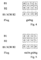
- Fig. 1 shows a state flag according to a preferred embodiment of the invention.
- the state flag (Flag) consists of two bit fields B1, B2 each with eight bits.
- the first line a) of Fig. 1 shows the state flag (Flag) in its initial state, in which it is after a reset by means of the reset means, without having been switched again after resetting. All bits have the logic value "1", so that both bit fields B1, B2 have the same number of eight “ones" and zero "zeroes".
- each pair of corresponding bits (memory cells) of the two bit fields B1, B2 has the same state, ie the first bit (from left) of the first bit field B1 has the same state as the first bit (from left) of the second bit field B2, the second bit (from left) of the first bit field B1 has the same state as the second bit (from the left) of the second bit field B2, the third bit (from the left) of the first bit field B1 has the same state as the third bit (from the left) of the second bit field B2 etc.
- the state value of the state flag (flag) is not valid, ie the flag is cleared, ie not set.
- the second line b) of Fig. 1 shows the state flag after it has been set, ie after its state value has been set to "set".
- the first bit of the first bit field B1 (framed) has been switched from “1" to "0".
- the bit field B1 now has seven ones and one zero.
- the state value of the state flag is consequently valid or set.
- the first bit of the first bit field B1 (state value "0") has a different state than the first bit of the second bit field B2 (state value "1").
- the state flag (Flag) also set according to this criterion (valid).
- the third line c) of Fig. 1 shows the state flag after it has been cleared again after being set from line b), ie, after its state value has been set to not set (cleared).
- the first bit of the second bit field B2 (framed) has been switched from “1" to "0".
- the first bit field B1 still has seven ones and one zero.
- the second bit field B2 now also has seven ones and a zero. Therefore, the two bit fields B1, B2 have the same number of ones and zeros, respectively.
- the state value of the state flag is thus invalid or not set.
- line c) of Fig. 1 the first bit of the first bit field B1 and the first bit of the second bit field B2 (again) the same state.
- the first pair of corresponding bits (memory cells) thus has (again) the same state, so that all corresponding bits (memory cells) have the same state.
- the fourth line d) of Fig. 1 shows the state flag after it has been reset, following deletion from line c).
- the second bit of the first bit field B1 (framed) has been switched from "1" to "0". Therefore, the two bit fields B1, B2 have a different number of ones. The state value of the state flag is thus invalid or not set.
- the second bit of the first bit field B1 (framed, state value "0") and the second bit of the second bit field B2 (state value "1") have a different one Status.
- the corresponding second bits of the two bit fields B1, B2 thus have a different state. All other corresponding pairs (first, third, fourth, ... eighth corresponding pair) of bits each have the same state, namely to the left of the current (here second) bit with state value "1", to the right of state value "0".
- the state flag can be set six more times and deleted seven times, ie a total of eight times, ie as many as each bit field has bits, set and deleted.
- one bit in the first bit field B1 and one bit in the second bit field B2 are alternately switched.
- the adjacent bits are switched in sequence, ie first the first bit, then the second bit, then the third bit, then the fourth bit etc.
- the last bit as in the last line o ) from Fig. 1 is shown, the last bit (framed) of the second bit field B2 switched. Only then are all bits set to "zero", and the state flag must be reset (reset) to that in line a) of Fig. 1 restore restored state.
- the memory device has a logic unit, in particular an XOR logic unit, from the configuration of the partial identifiers (bit fields).
- the logic unit is set up to link corresponding memory cells of the first and the second component identifier and to output the result of the combination as the status value of the status identifier.
- FIG. 4 and FIG. 5 illustrate the operation of a logic unit according to the invention in the form of an XOR logic unit.
- Fig. 4 shows the operation of an XOR logic unit using the example of a valid (set) flag.
- Fig. 5 shows how the XOR logic unit works using the example of an invalid (not set, deleted) flag.
- the first two lines of the FIGS. 4 and 5 each show a state flag with two bit fields B1 and B2 according to a similar embodiment of the state flag as in FIG Fig. 1 shown, but with only four bits per bit field B1, B2.
- the flag off Fig. 4 is set (valid) since the second bit of the first memory field B1 has the state value "1" and the second bit of the second memory field B2 has the state value "0", so that the two corresponding second bits have different state values.
- the bitwise XOR combination of the two bit fields results in the bit sequence shown in the third line. Since one of the four bits, here the second bit, is different from zero, the flag is considered set (valid), as shown in the fourth line. The flag would be considered set even if, in the third row, another one of the four bits, that is, the first, third or fourth bit, would be different from zero (in Fig. 4 Not shown).
- the flag off Fig. 5 is not set (invalid) since all four pairs of corresponding bits have the same state value, namely "zero" for the two corresponding first bits and the two corresponding second bits, and "one" for the two corresponding third bits and the two corresponding ones fourth bits.
- the bitwise XOR combination of the two bit fields results in the bit sequence shown in the third line. Since all bits are zero, the flag is considered not set (invalid), as shown in the fourth line.
- Fig. 2 shows, according to one embodiment of the invention, the process flow when writing (copying) new data to a file, with prior buffering of the original data that was originally present in the file.
- Fig. 3 schematically shows the temporal and spatial sequence of the copying processes in the process Fig. 2 ,
- a file contains original data. Now, new data will be copied to the file and saved there, overwriting the original data.
- a buffer is available that has a flag that allows the data in the buffer to be marked as valid or invalid.
- the original data of the file is copied into the buffer memory ( Fig. 2, Fig. 3 ).
- the flag of the buffer memory is set to valid ( Fig. 2 ). This can be done, for example, by a switching operation (2) like that in line b) of Fig. 1 are shown, in which the first bit of the first bit field B1 is switched.
- a third step (3) the new data is copied to the file and stored there ( Fig. 2, Fig. 3 ).
- a fourth step (4) the buffer memory flag is set to invalid ( Fig. 2 ). This can, for example, by a switching operation (4) as in line c) of Fig. 1 are shown, in which the first bit of the second bit field B2 is switched. If a process aborts while the flag is set, resuming the process writes the data from the buffer to the file. If, on the other hand, the flag is cleared when the process aborts, the data contained in the file will be retained when the process is resumed.
- a first step (5) the original data of the file is copied to the buffer ( Fig. 2, Fig. 3 ).
- step (6) the flag of the buffer memory is set to valid ( Fig. 2 ). This can be done, for example, by a switching process (6) like that in line d) of Fig. 1 are shown, in which the second bit of the first bit field B1 is switched.
- the memory device further additionally has a reset safety unit, which is set up to check the state flag for consistency in accordance with a predetermined structure having the state flag.
- the reset protection unit can prevent the flag from reaching an indeterminate state if, during operation, e.g. during the set or reset, an interruption occurs, in particular an interruption of the supply voltage. Which state of the state flag is consistent and which is not is predetermined by the structure of the state flag.
- the consistency preferably comprises, within each sub-tag, at most a single pair of adjacent memory cells having different state values. In this way, it is ensured that the memory cells have values as generated by a proper bitwise, sequential write in which adjacent memory cells within a sub-tag are sequentially (ie, in an order first, second, third, etc. memory cell ).
- the reset security unit is preferably further configured to cause or effect a reset of the state flag to the initial value if the check results in a lack of consistency. If the reset is effected, preferably all facilities required for this purpose are present at the memory device, and further preferably integrated in a data carrier such as a chip card or a token. If the reset is merely initiated, optionally at least a portion of the devices required to effect the reset are provided separately from the memory device and, if the memory device is integrated with a data carrier such as a smart card or a token, external to the data carrier.
- the status flag is recognized as inconsistent.
- the status code is reset to the initial value (eg "11111111").
- a logically linear arrangement of the memory cells is understood to mean that the memory cells are logically juxtaposed so that they form a linear sequence of memory cells, for example a memory word or a plurality of memory words or the like, wherein the memory cells do not necessarily have to be physically adjacent to one another.
- a write operation preferably has a write duration in the range of about 1 to about 20 ⁇ s, more preferably about typically 7 ⁇ s and a maximum of 10 ⁇ s
- an erase operation has an erase duration in the range of about 1 ms to about 50 ms, more preferably typically about 18 ms and a maximum of 25 ms, or vice versa.
- the programming voltage is preferably for writing in the voltage range of 1V to 4V, preferably at about 3.0V to 3.6V and for erasing in the voltage range of 5V to 16V, preferably at about 10V, or vice versa.
- the programming voltage is preferably equal to the voltage applied to the single memory cell voltage, which may be different from the externally applied voltage, wherein the voltage applied to the memory cell is preferably generated in a conventional manner from the externally applied voltage.
- the externally applied voltage is, for example, the output voltage of a voltage source.
- the mentioned parameter values are example values. Depending on the memory used, the parameter values may also be in other ranges.
Abstract
Description
Die Erfindung betrifft eine Speichereinrichtung mit einem eine Mehrzahl von Speicherzellen aufweisenden, bezüglich des Schreibens und Löschens asymmetrischen elektronischen Speicher mit mindestens einem in dem Speicher implementierten Zustandskennzeichen (Flag), das wahlweise einen ersten (gesetzten, gültigen) Zustandswert oder einen zweiten (nicht gesetzten, ungültigen) Zustandswert haben kann, und das zwischen dem ersten und dem zweiten Zustandswert schaltbar ist.The invention relates to a memory device having an asymmetrical electronic memory having a plurality of memory cells with at least one state flag implemented in the memory, which optionally has a first (set, valid) state value or a second (unset, invalid) state value, and that is switchable between the first and the second state value.
Ein elektronischer Speicher ist in der Regel in eine Mehrzahl von Speicherzellen unterteilt. Beim Programmieren des Speichers, d.h. Schreiben oder Löschen von Speicherinhalten, werden die einzelnen Speicherzellen von einem ersten Speicherzustand, beispielsweise einer logischen "1 ", in einen zweiten Speicherzustand, beispielsweise eine logische "0", gebracht und umgekehrt, wozu Löschvorgänge und Schreibvorgänge durchgeführt werden. Welcher Zustand von dem gelöschten und dem beschriebenen Speicherzustand dabei eine logische "1" und welcher eine logische "0" ist, ist in der Regel frei wählbar und wird in der Regel bereits durch den Hersteller des Speichers festgelegt.An electronic memory is usually divided into a plurality of memory cells. When programming the memory, i. Writing or erasing memory contents, the individual memory cells are brought from a first memory state, for example a logical "1", to a second memory state, for example a logical "0", and vice versa, for which erasures and writes are performed. Which state of the deleted and the described memory state while a logical "1" and which is a logical "0" is usually arbitrary and is usually already determined by the manufacturer of the memory.
Eine Mehrzahl von elektronischen Speichern, z.B. EEPROM, Flash-ROM (Flash-EEPROM), sind bezüglich des Schreibens und des Löschens von Daten asymmetrisch, indem beispielsweise die Zeitdauer, die zum Löschen des Speichers erforderlich ist (Löschzeit oder Löschdauer), unterschiedlich ist von der Zeitdauer, die zum Beschreiben des Speichers erforderlich ist (Schreibzeit oder Schreibdauer). Alternativ oder zusätzlich kann der Stromverbrauch beim Schreiben unterschiedlich sein vom Stromverbrauch beim Löschen. Bei einer Mehrzahl von Speichern ist beispielsweise die Programmierspannung, die zum Programmieren angelegt werden muss, unterschiedlich, je nachdem, ob der Speicher beschrieben oder gelöscht wird. Unter der Programmierspannung ist hierbei die tatsächlich bei der Speicherzelle anliegende Spannung zu verstehen, die von einer äußeren, von einer Spannungsquelle erzeugten Spannung, die zur Erzeugung der Programmierspannung verwendet wird, unterschiedlich sein kann.A plurality of electronic memories, eg, EEPROM, Flash-ROM (Flash EEPROM), are asymmetric in writing and erasing data, for example, by making the time required for erasing the memory (erasing time or erasing time) different from the amount of time required to write to the memory (write time or write duration). Alternatively or additionally, the power consumption during writing may be different from the power consumption when deleting. For example, in a plurality of memories, the programming voltage to be applied for programming is different, depending on whether the memory is written or deleted. The programming voltage here is to be understood as meaning the voltage actually applied to the memory cell which may be different from an external voltage generated by a voltage source which is used to generate the programming voltage.
Bei einem bekannten Flash-EEPROM-Speicher vom Typ NOR-Flash des Herstellers Silicon Storage Technology SST ist für eine einzelne Speicherzelle "1" ("Eins") der gelöschte Zustand und "0" ("Null") der beschriebene Zustand. Bei diesem Flash-EEPROM dauert das Schreiben, bei dem einzelne Speicherzellen von logisch "1" auf logisch "0" umprogrammiert werden, ungefähr 50 µs, wohingegen das Löschen von Speicherzellen, das beim Flash-Speicher i.d.R. in Einheiten von Pages oder Blocks durchgeführt wird, und bei dem die Speicherzellen von logisch "0" auf logisch "1" umprogrammiert werden, ungefähr zwei bis maximal fünf ms dauert.For a single memory cell, "1" ("one") is the erased state and "0" ("zero") is the state described in a known NOR Flash flash EEPROM memory manufactured by Silicon Storage Technology SST. In this flash EEPROM, the writing in which individual memory cells are reprogrammed from logic "1" to logic "0" takes about 50 μs, whereas the erasing of memory cells stored in the flash memory i.d.R. in units of pages or blocks, and in which the memory cells are reprogrammed from logic "0" to logic "1", takes about two to a maximum of five ms.
Für unterschiedliche Operationen, wie beispielsweise Programmiervorgänge, in einem Speicher ist es erforderlich, dass der Zustand eines vorbestimmten Speicherabschnitts bekannt ist, damit beispielsweise der Zustand als Bedingung für nachfolgende Operationsschritte verwendet werden kann. Der Zustand des Speicherabschnitts ist hierbei durch ein Zustandskennzeichen oder gleichbedeutend Flag markiert. In Abhängigkeit vom Zustandswert (Flag-Wert) kann beispielsweise das Schreiben (oder das Lesen) in dem Speicherabschnitt entweder verboten oder erlaubt sein. Gegenstand der Erfindung ist ein Zustandskennzeichen oder Flag in diesem Sinne, also ein Kennzeichen durch das ein Zustand angezeigt ist.For different operations, such as programming operations, in a memory, it is necessary that the state of a predetermined memory section is known, for example, so that the state can be used as a condition for subsequent operation steps. The state of the memory section is hereby marked by a state flag or equivalent flag. For example, depending on the state value (flag value), writing (or reading) in the memory section may be either prohibited or allowed. The subject matter of the invention is a status code or flag in this sense, that is to say a code by which a status is indicated.
Flags werden beispielsweise häufig bei sogenannten atomaren Schreibvorgängen benutzt, die sich dadurch auszeichnen, dass sie nur entweder vollständig oder gar nicht ausgeführt werden dürfen. Ein Beispiel für einen solchen atomaren Schreibvorgang stellt das Schreiben von Daten in eine Chipkarte dar, beispielsweise um einen Fehlbedienungszähler zu aktualisieren oder um eine elektronische Geldbörse mit einer Zahlung zu belasten (
Kommt es nun, abweichend vom vorstehend beschriebenen Fall, in dem der atomare Schreibvorgang erfolgreich vollständig durchgeführt worden ist, während des Ablaufs des Schreibvorgangs zu einem Abbruch, verursacht beispielsweise durch eine Unterbrechung der Betriebsspannung, so kann bei der nächsten Inbetriebnahme der Chipkarte das Zustandskennzeichen (Flag) dabei verwendet werden, den Speicherinhalt des Speicherabschnitts der Chipkarte bei Bedarf wiederherzustellen. Falls das Zustandskennzeichen (Flag) des Pufferspeichers gesetzt, d.h. "auf gültig gesetzt", ist, werden die Daten aus dem Pufferspeicher, d.h. die ursprünglichen Daten, wieder in den Speicherabschnitt geschrieben, da zuvor die neuen Daten noch nicht vollständig einprogrammiert worden sind. Die neuen Daten müssen nochmals eingeschrieben werden. Im Fall einer elektronischen Geldbörse wird also der Geldbetrag, der vor dem teilweise fehlgeschlagenen Belastungsvorgang (Verringerung des Geldbetrags) dort vorhanden war, in der elektronischen Geldbörse wiederhergestellt. Die Belastung muss nochmals vorgenommen werden. Falls hingegen das Zustandskennzeichen (Flag) des Pufferspeichers gelöscht, d.h. nicht gesetzt oder "auf ungültig gesetzt", ist, zeigt dies an, dass die Daten zuvor vollständig in den Speicherabschnitt geschrieben worden sind. Die ursprünglichen Daten im Pufferspeicher werden daher nicht zurück in den Speicherabschnitt geschrieben. Im Beispiel der elektronischen Geldbörse wird der neue, verringerte Geldbetrag beibehalten.If, deviating from the case described above, in which the atomic writing process has been successfully completed, during the execution of the writing process, an abort caused, for example, by an interruption of the operating voltage, the status flag (flag ) be used to restore the memory contents of the memory portion of the smart card when needed. If the state flag of the buffer memory is set, ie "set to valid", the data from the buffer memory, ie the original data, is written back into the memory section, since previously the new data has not yet been completely programmed in. The new data must be re-registered. In the case of an electronic wallet, therefore, the amount of money that was there before the partially failed debit process (reduction of the amount of money) there was restored in the electronic purse. The load must be repeated. On the other hand, if the state flag of the buffer memory is cleared, ie, not set or "set to invalid," this indicates that the data has previously been completely written to the memory section. The original data in the buffer memory is therefore not written back to the memory section. In the example of the electronic wallet, the new, reduced amount of money is retained.
Zustandskennzeichen (Flags) werden außer bei atomaren Schreibvorgängen und Lesevorgängen auch bei einer Vielzahl von weiteren unterschiedlichen Operationen eingesetzt.State flags are also used in a variety of other different operations except for atomic writes and reads.
Ein herkömmliches Zustandskennzeichen (Flag) besteht aus einer einzelnen Speicherzelle, z.B. einem einzelnen Bit, die auf Null "0" oder Eins "1" gesetzt ist, je nachdem, ob der Zustandswert des Zustandskennzeichens (Flags) gültig (Flag gesetzt) oder ungültig (Flag nicht gesetzt) ist.A conventional state flag consists of a single memory cell, e.g. a single bit set to zero "0" or one "1" depending on whether the state flag state flag is valid (flag set) or invalid (flag not set).
Bei einem Speicher, der bezüglich des Schreibens (Schreibvorgänge) und des Löschens (Löschvorgänge) asymmetrisch ist, hat ein solches Zustandskennzeichen (Flag) aus einer einzelnen Speicherzelle den Nachteil, dass das Zustandskennzeichen bezüglich des Schaltens, d.h. bezüglich des Setzens (auf gültig Setzens) und Löschens (auf ungültig Setzens) des Zustandskennzeichens asymmetrisch ist.For a memory that is asymmetric in terms of writing (writing) and erasing (erasing), such a flag of a single memory cell has the disadvantage that the state flag with respect to the switching, ie with respect to the setting (on valid setting) and deleting (on invalid setting) of the state flag is asymmetric.
Beispielsweise muss zum Setzen des Zustandskennzeichens (Flags) ein anderer, unterschiedlicher Spannungswert an die Speicherzelle angelegt werden als zum Löschen des Zustandskennzeichens (Flags). Alternativ oder zusätzlich sind die Programmierdauern für das Setzen und Löschen des Zustandskennzeichens (Flags) unterschiedlich. In beiden Fällen ist die Ansteuerelektronik zum Schalten, d.h. Setzen bzw. Löschen, des Zustandskennzeichens (Flags) aufwändig und daher teuer, da sie eine Fallunterscheidung vornehmen muss, ob ein Schreibvorgang oder ein Löschvorgang durchgeführt werden soll.For example, to set the state flag, another different voltage value must be applied to the memory cell than to clear the state flag. Alternatively or additionally, the programming periods for setting and deleting the state flag (flags) are different. In both cases, the drive electronics for switching, i. Setting or deleting the state flag (flags) consuming and therefore expensive, since they must make a case distinction, whether a write or erase operation should be performed.
Aus
Eine Speichereinrichtung nach dem Oberbegriff der Ansprüche 1 und 16 ist aus der
Aufgabe der Erfindung ist es, eine Speichereinrichtung der eingangs genannten Art zu schaffen, die ein effizienteres Schalten des Zustandskennzeichens ermöglicht, und ein entsprechendes Kennzeichnungsverfahren unter Verwendung eines Zustandskennzeichen zu schaffen.The object of the invention is to provide a memory device of the type mentioned, which allows a more efficient switching of the state flag, and to provide a corresponding identification method using a state flag.
Die Aufgabe wird gelöst durch eine Speichereinrichtung nach dem unabhängigen Anspruch 1 und durch ein Verfahren nach dem unabhängigen Anspruch 16. Vorteilhafte Ausgestaltungen der Erfindung sind in den abhängigen Ansprüchen angeführt.The object is achieved by a memory device according to the
Die erfindungsgemäße Speichereinrichtung gemäß dem unabhängigen Anspruch 1, bzw. das erfindungsgemäße Verfahren gemäß dem unabhängigen Anspruch 16, hat, bzw. bezieht sich auf einen elektronischen Speicher mit einer Mehrzahl von binären Speicherzellen. Jede Speicherzelle ist durch einen Programmiervorgang zwischen einem gelöschten und einem beschriebenen Zustand schaltbar, wobei durch einen Löschvorgang der gelöschte Zustand herstellbar ist und durch einen Schreibvorgang der beschriebene Zustand herstellbar ist. Der Speicher ist bezüglich Schreibvorgängen und Löschvorgängen asymmetrisch, wobei dies genauer bedeutet, dass bei einem Schreibvorgang ein oder mehrere Programmierparameter einen anderen (unterschiedlichen) Wert haben als bei einem Löschvorgang. Zu den Programmierparametern können zählen: die Programmierdauer, d.h. die Zeitdauer, die erforderlich ist, um einen vollständigen Programmiervorgang, insbesondere Schreibvorgang oder Löschvorgang, durchzuführen; die Programmierspannung, d.h. die Spannung, die an den Speicher, insbesondere an jede einzelne Speicherzelle, angelegt werden muss, um einen Programmiervorgang durchzuführen.The memory device according to the invention according to the
In dem Speicher ist weiter mindestens ein Zustandskennzeichen (Flag) implementiert, das wahlweise einen ersten (gesetzten, gültigen) Zustandswert oder einen zweiten (gelöschten, ungültigen, nicht gesetzten) Zustandswert haben kann. Weiter weist die Speichereinrichtung eine Schalteinrichtung auf, mit der der Wert des Zustandskennzeichens zwischen dem ersten und dem zweiten Zustandswert schaltbar ist, wobei zum Schalten des Zustandswerts mindestens ein Programmiervorgang an mindestens einer Speicherzelle durchgeführt wird. Gemäß der Erfindung ist die Schalteinrichtung, mit der sich der Wert des Zustandskennzeichens schalten, d.h. wahlweise setzen und löschen, lässt, derart implementiert, dass zum Schalten vom ersten zum zweiten Zustandswert und zum Schalten vom zweiten zum ersten Zustandswert die gleiche Art von Programmiervorgang, insbesondere Schreibvorgang oder Löschvorgang, durchgeführt wird. Insbesondere wird beispielsweise sowohl zum Setzen des Flag als auch zum Löschen des Flag ein Schreibvorgang an einer Speicherzelle durchgeführt. Alternativ wird sowohl zum Setzen des Flag als auch zum Löschen des Flag ein Löschvorgang an einer Speicherzelle durchgeführt.The memory is further implemented with at least one state flag which may optionally have a first (set, valid) state value or a second (deleted, invalid, not set) state value. Furthermore, the memory device has a switching device with which the value of the state identifier can be switched between the first and the second state value, at least one programming process being performed on at least one memory cell for switching the state value. According to the invention, the switching means with which the value of the state flag can be switched, ie selectively set and cleared, is implemented such that the same type of programming operation for switching from the first to the second state value and to the switching from the second to the first state value Write or delete operation is performed. In particular, for example, both for setting the flag and for deleting the flag, a write operation is performed on a memory cell. Alternatively, both to set the flag and to clear the flag, an erase operation is performed on a memory cell.
Die erfindungsgemäße Speichereinrichtung hat den Vorteil, dass das Zustandskennzeichen (Flag) bezüglich seines Setzens und Löschens symmetrisch ist. D.h. insbesondere haben die ein oder mehreren Programmierparameter wie Programmierdauer und/ oder Programmierspannung beim Löschen und beim Setzen den gleichen Wert. Hierdurch braucht keine Fallunterscheidung danach getroffen werden, ob das Zustandskennzeichen (Flag) gesetzt oder gelöscht wird, so dass eine Schalteinrichtung mit einem einfachen Aufbau verwendet werden kann. Das Schalten des Zustandskennzeichens ist hierdurch effizienter als bei bekannten Speichereinrichtungen.The memory device according to the invention has the advantage that the state flag (flag) is symmetrical with respect to its setting and erasing. That In particular, the one or more programming parameters such as program duration and / or program voltage have the same value when cleared and set. As a result, no case discrimination needs to be made on whether the flag is set or cleared, so that a switch can be used with a simple structure. The switching of the state flag is thereby more efficient than in known memory devices.
Daher ist gemäß Anspruch 1 eine Speichereinrichtung geschaffen, die ein effizienteres Schalten des Zustandskennzeichens ermöglicht.Therefore, according to
Vorzugsweise wird zum Setzen und zum Löschen des Zustandskennzeichens (Flag) jeweils genau ein Programmiervorgang an genau einer Speicherzelle durchgeführt.Preferably, precisely one programming operation is carried out on exactly one memory cell for setting and for deleting the status code (flag).
Der Speicher kann insbesondere beispielsweise ein (gewöhnlicher) EEPROM oder ein Flash-EEPROM (Flash-ROM) sein, der im genannten Sinn asymmetrisch ist.Specifically, the memory may be, for example, an EEPROM or a Flash EEPROM (Flash ROM), which is asymmetric in the above sense.
Die Komponenten der erfindungsgemäßen Speichereinrichtung, wie das Zustandskennzeichen und die Schalteinrichtung, können in Softwareform, in Hardwareform oder teils in Softwareform, teils in Hardwareform implementiert sein. Vorzugsweise sind das Zustandskennzeichen und die Schalteinrichtung und ggf. weitere Komponenten in Softwareform implementiert.The components of the memory device according to the invention, such as the status code and the switching device, can be implemented in software form, in hardware form or partly in software form, partly in hardware form. Preferably, the state identifier and the switching device and possibly other components are implemented in software form.
Die Asymmetrie bezüglich Schreibvorgängen und Löschvorgängen umfasst gemäß einer Ausführungsform der Erfindung, dass ein Schreibvorgang eine kürzere Programmierdauer hat (kürzer dauert) als ein Löschvorgang oder umgekehrt. Vorzugsweise wird bei dieser Ausführungsform von der Schalteinrichtung zum Schalten zwischen dem ersten und zweiten Zustandswert des Zustandskennzeichens (Flag) derjenige Programmiervorgang von dem Schreibvorgang und dem Löschvorgang verwendet wird, der eine kürzere Programmierdauer hat. Diese bevorzugte Ausführungsform hat den weiteren Vorteil, dass das Zustandskennzeichen zum Schalten seines Zustandswerts nur "schnelle" Programmiervorgänge verwendet. Hierdurch ist das Zustandskennzeichen besonders zeitsparend und daher effizient.The asymmetry with respect to write operations and deletions comprises, according to an embodiment of the invention, a write operation of a has a shorter programming time (shorter) than a deletion or vice versa. Preferably, in this embodiment, the switching means for switching between the first and second state values of the flag (Flag) uses the programming operation of the writing operation and the erasing operation having a shorter programming period. This preferred embodiment has the further advantage that the state flag only uses "fast" programming operations to switch its state value. As a result, the state indicator is particularly time-saving and therefore efficient.
Gemäß einer anderen Ausführungsform der Erfindung umfasst die Asymmetrie bezüglich Schreibvorgängen und Löschvorgängen, dass ein Schreibvorgang eine andere, unterschiedliche (höhere oder niedrigere) Programrnierspannung benötigt als ein Löschvorgang. Vorzugsweise wird beim Schalten des Zustandskennzeichens derjenige Programmiervorgang verwendet, der die niedrigere Programmierspannung benötigt. Diese bevorzugte Ausführungsform hat den weiteren Vorteil, dass das Zustandskennzeichen beim Schalten seines Zustandswerts besonders stromsparend ist.According to another embodiment of the invention, the asymmetry of writes and erasures involves a write requiring a different (higher or lower) program voltage than an erase. Preferably, when switching the state flag that programming operation is used which requires the lower programming voltage. This preferred embodiment has the further advantage that the state flag is particularly energy-saving when switching its state value.
Vorzugsweise hat die Speichereinrichtung weiter eine Rücksetzeinrichtung, mit der ein Ausgangszustand des Zustandskennzeichens einstellbar ist. Ausgehend vom Ausgangszustand ist mindestens ein Schaltvorgang zum Schalten, insbesondere Setzen oder Löschen, des Zustandskennzeichens (Flag) möglich. Vorzugsweise, in Abhängigkeit von der genaueren Gestaltung des Zustandskennzeichens, ist ausgehend vom Ausgangszustand eine Mehrzahl von aufeinanderfolgenden Schaltvorgängen möglich, bei denen der Zustandswert des Zustandskennzeichens abwechselnd zwischen gültig und ungültig geschaltet wird, d.h. abwechselnd immer einmal von ungültig zu gültig und einmal von gültig zu ungültig geschaltet wird. Dabei wird, gemäß der Erfindung, zum Schalten jeweils die gleiche Art von Programmiervorgang verwendet, unabhängig davon, ob das Zustandskennzeichen auf gültig oder auf ungültig geschaltet wird.Preferably, the memory device further has a reset device, with which an output state of the state flag is adjustable. Starting from the initial state, at least one switching operation for switching, in particular setting or clearing, of the state flag (flag) is possible. Preferably, depending on the more detailed design of the state flag, a plurality of successive switching operations is possible starting from the initial state in which the state value of the state flag alternately between valid and invalid, ie alternately always from invalid to valid and once from valid to invalid is switched. In doing so, According to the invention, the same type of programming operation is used for switching, regardless of whether the state flag is switched to valid or to invalid.
Die Rücksetzeinrichtung ist weiter vorzugsweise derart implementiert, dass sie zum Einstellen des Ausgangszustands den anderen Programmiervorgang von dem Schreibvorgang und dem Löschvorgang verwendet, als er zum Schalten zwischen dem ersten und dem zweiten Zustandswert des Zustandskennzeichens (Flag) verwendet wird.The reset means is also preferably implemented to use the other programming operation of the write and erase operations to set the output state than is used to switch between the first and second state values of the flag.
Beispielsweise wird also zum Schalten des Zustandskennzeichens (Flag) ein Schreibvorgang an einer Speicherzelle verwendet und zum Einstellen des Ausgangszustands mittels der Rücksetzeinrichtung ein Löschvorgang verwendet oder umgekehrt.For example, therefore, a write operation to a memory cell is used to switch the state flag (Flag) and an erase operation is used to set the output state by means of the reset device or vice versa.
Gemäß einer bevorzugten Ausführungsform wird zum Schalten des Zustandskennzeichens (Flag) der schnellere Programmiervorgang verwendet, bei dem die Programmierdauer niedriger ist, wohingegen zum Einstellen des Ausgangszustands mittels der Rücksetzeinrichtung der langsamere Programmiervorgang verwendet wird, bei dem die Programmierdauer höher ist. Diese Ausführungsform hat den weiteren Vorteil, dass der langsame Programmiervorgang ausschließlich beim Rücksetzen angewandt wird, das in der Regel seltener durchgeführt wird als das Schalten des Zustandskennzeichens (Flag). Beim in der Regel häufiger durchgeführten Schalten des Zustandskennzeichens (Flag), d.h. beim Setzen und Löschen, wird der schnelle Programmiervorgang verwendet.According to a preferred embodiment, to switch the state flag (Flag) the faster programming operation is used, in which the programming time is lower, whereas for setting the initial state by means of the reset means the slower programming operation is used, in which the programming time is higher. This embodiment has the further advantage that the slow programming operation is applied exclusively to the reset, which is usually performed less frequently than the switching of the state flag. In the usually more frequent switching of the state flag, i. when setting and deleting, the fast programming process is used.
Alternativ oder zusätzlich wird zum Schalten des Zustandskennzeichens (Flag) der stromsparendere Programmiervorgang verwendet, bei dem eine geringere Programmierspannung an die Speicherzelle(n) angelegt werden muss, wohingegen zum Einstellen des Ausgangszustands mittels der Rücksetzeinrichtung der stromintensivere Programmiervorgang verwendet wird, bei dem eine höhere Programmierspannung an die Speicherzelle(n) angelegt werden muss. Hierdurch ist der stromintensive Programmiervorgang nur bei dem selteneren Rücksetzen des Zustandskennzeichens (Flag) im Einsatz, beim Schalten (Setzen, Löschen) des Zustandskennzeichens (Flag) wird dagegen der stromsparende Programmiervorgang verwendet.Alternatively or additionally, for switching the state flag (Flag) of the power-saving programming process is used, in which a lower programming voltage must be applied to the memory cell (s), whereas to set the output state by means of the reset means the more current-intensive programming operation is used, in which a higher programming voltage must be applied to the memory cell (s). As a result, the power-intensive programming operation is only in the rare reset the state flag (flag) in use, when switching (set, clear) of the state flag (Flag), however, the power-saving programming process is used.
Eine bevorzugte Verwendung der Speichereinrichtung gemäß der Erfindung ist in einem Datenträger wie einer Chipkarte oder einem Token, mit einem elektronischen Schaltkreis, in dem die Speichereinrichtung implementiert ist. Die Chipkarte kann eine kontaktlose oder kontaktbehaftete oder sowohl kontaktlos als auch kontaktbehaftet betreibbare Chipkarte mit einem beliebigen Format, z.B. nach ISO 7810, z.B. ID-1 (Scheckkartenformat) oder ID-000 (SIM-Karten- oder Minikarten-Format) oder ID-00 oder nach GSM 11.1 oder TS 102.221 oder nach einer anderen Norm, oder nach keiner Norm. Der Token kann jedes beliebige Gehäuse und jede beliebige Schnittstelle (kontaktlos, kontaktbehaftet, seriell, USB etc.) haben.A preferred use of the memory device according to the invention is in a data carrier such as a chip card or a token, with an electronic circuit in which the memory device is implemented. The chip card can be a contactless or contact-type or both contactless and contact-operated chip card of any format, e.g. according to ISO 7810, e.g. ID-1 (credit card size) or ID-000 (SIM card or mini-card format) or ID-00 or GSM 11.1 or TS 102.221 or other standard, or no standard. The token can have any housing and any interface (contactless, contact-type, serial, USB, etc.).
Im folgenden wird die Erfindung an Hand von Ausführungsbeispielen und unter Bezugnahme auf die Zeichnung näher erläutert, in der zeigen:
- Fig. 1
- ein Zustandskennzeichen (Flag) gemäß einer Ausführungsform der Erfindung, mit zwei Bitfeldern B1, B2;
- Fig. 2
- den Verfahrensablauf beim Schreiben (Kopieren) von neuen Daten in eine Datei, mit vorherigem Puffern der ursprünglichen Daten in der Datei, gemäß einer Verwendung der Erfindung;
- Fig. 3
- eine schematische Darstellung der Kopiervorgänge der ursprünglichen Daten von der Datei in den Pufferspeicher und der neuen Daten in die Datei, bei dem Verfahren aus
Fig. 2 ; - Fig. 4
- die Funktionsweise einer XOR-Logikeinheit zur Ermittlung des Zustandswerts eines Flag am Beispiel eines gültigen (gesetzten) Flag;
- Fig. 5
- die Funktionsweise der XOR-Logikeinheit aus
Fig. 4 am Beispiel eines ungültigen (nicht gesetzten, gelöschten) Flag.
- Fig. 1
- a state flag (Flag) according to an embodiment of the invention, with two bit fields B1, B2;
- Fig. 2
- the process of writing (copying) new data to a file, with prior buffering of the original data in the file, according to one use of the invention;
- Fig. 3
- a schematic representation of the copying operations of the original data from the file in the buffer and the new data in the file, in the method off
Fig. 2 ; - Fig. 4
- the operation of an XOR logic unit for determining the state value of a flag using the example of a valid (set) flag;
- Fig. 5
- the functioning of the XOR logic unit
Fig. 4 the example of an invalid (not set, deleted) flag.
Gemäß Ausführungsformen der Erfindung hat das Zustandskennzeichen mindestens ein Paar von zwei Teilkennzeichen, wobei jedes Teilkennzeichen des Paars mindestens eine Speicherzelle aufweist. Das Zustandskennzeichen aus
Ein erfindungsgemäßer Flash-Speicher mit dem Zustandskennzeichen mit den beiden Teilkennzeichen ist vorzugsweise in Pages eingeteilt, wobei beim Löschen des Speichers jeweils eine Pages auf einmal gelöscht wird. Jedes der beiden Teilkennzeichen hat bei dem Flash-Speicher vorzugsweise eine Anzahl von Speicherzellen, die gleich einem ganzzahligen Teiler der Pagegröße (Anzahl Speicherzellen pro Page) ist, so dass also eine einzelne Page durch eine ganze Zahl von Teilkennzeichen vollständig gefüllt werden kann. Weiter vorzugsweise ist die Größe des Teilkennzeichens (Anzahl Speicherzellen im Teilkennzeichen) gleich einem ganzzahligen Teiler der halben Pagegröße ist, so dass also eine einzelne Page durch eine ganze Zahl von Zustandskennzeichen mit je zwei Teilkennzeichen vollständig gefüllt werden kann.A flash memory according to the invention with the status code with the two partial identifiers is preferably divided into pages, with one page being deleted at a time when the memory is deleted. Each of the two sub-flags preferably has a number of memory cells equal to an integer divisor of the page size (number of memory cells per page) in the flash memory, so that a single page can be completely filled by an integer number of sub-flags. Further preferably, the size of the partial identifier (number of memory cells in the partial identifier) is equal to an integer divisor of half the page size, so that a single page can be completely filled by an integer number of state identifiers with two partial identifiers.
Bei einer bevorzugten Ausführungsform eines Zustandskennzeichens mit einem Paar von (zwei) Teilkennzeichen ist der erste Zustandswert dadurch ausgezeichnet, dass in jedem Teilkennzeichen des Paars die gleiche Anzahl von Speicherzellen den gelöschten und/oder den beschriebenen Zustand hat, wobei der zweite Zustandswert bei dieser Ausführungsform dadurch ausgezeichnet ist, dass in jedem Teilkennzeichen des Paars eine unterschiedliche Anzahl von Speicherzellen den gelöschten und/ oder den beschriebenen Zustand hat. Weiter vorzugsweise bilden die einzelnen Speicherzellen des ersten Teilkennzeichens mit den einzelnen Speicherzellen des zweiten Teilkennzeichens Paare von korrespondierenden Speicherzellen, d.h. die erste (zweite, dritte, vierte, ...) Speicherzelle des ersten Teilkennzeichens korrespondiert mit der ersten (zweiten, dritten, vierten, ...) Speicherzelle des zweiten Teilkennzeichens. Bei dieser bevorzugten Variante ist der erste Zustandswert dadurch ausgezeichnet, dass in den beiden Teilkennzeichen korrespondierende Speicherzellen den gleichen Zustand haben, und der zweite Zustandswert dadurch ausgezeichnet, dass in den beiden Teilkennzeichen bei einem Paar von korrespondierenden Speicherzellen die beiden korrespondierenden Speicherzellen einen unterschiedlichen Zustand haben.In a preferred embodiment of a state flag having a pair of (two) sub-flags, the first state value is characterized in that in each sub-flag of the pair, the same number of memory cells have the erased and / or described states, the second state value in this embodiment it is excellent that in each sub-tag of the pair, a different number of memory cells have the erased and / or described state. Preferably, the individual memory cells of the first partial identifier form with the individual memory cells of the second partial identifier pairs of corresponding memory cells, ie the first (second, third, fourth,...) Memory cell of the first partial identifier corresponds to the first (second, third, fourth, ...) memory cell of the second part identifier. In this preferred variant, the first state value is distinguished in that corresponding memory cells have the same state in the two partial identifiers, and the second state value is distinguished by the fact that in the two partial identifiers in a pair of corresponding memory cells, the two corresponding memory cells have a different state.
Die erste Zeile a) von
Die zweite Zeile b) von
Die dritte Zeile c) von
Die vierte Zeile d) von
Nachfolgend kann das Zustandskennzeichen noch sechs Mal gesetzt und sieben Mal gelöscht werden, insgesamt also acht Mal, d.h. so oft wie jedes Bitfeld Bits hat, gesetzt und gelöscht werden. Dabei wird jeweils abwechselnd ein Bit im ersten Bitfeld B1 und ein Bit im zweiten Bitfeld B2 geschaltet. Innerhalb jedes einzelnen Bitfeldes B1 oder B2 werden die benachbarten Bits der Reihe nach geschaltet, d.h. erst das erste Bit, dann das zweite Bit, dann das dritte Bit, dann das vierte Bit etc.. Als letztes Bit wird, wie in der letzten Zeile o) von
Um bei einem Zustandskennzeichen mit zwei Teilkennzeichen, also insbesondere bei einem Zustandskennzeichen mit zwei Bitfeldern wie dem in
Das Flag aus
Das Flag aus
Zu Beginn des Verfahrens enthält eine Datei ursprüngliche Daten. Nun sollen in die Datei neue Daten kopiert und dort abgespeichert werden, wobei die ursprünglichen Daten überschrieben werden. Zum Puffern der ursprünglichen Daten steht ein Pufferspeicher zur Verfügung, der ein Flag hat, mit dem die Daten im Pufferspeicher als gültig oder ungültig markiert werden können. Nachdem der Vorgang eingeleitet worden ist, werden in einem ersten Schritt (1) die ursprünglichen Daten der Datei in den Pufferspeicher kopiert (
Bei einer bevorzugten Ausführungsform einer erfindungsgemäßen Speichereinrichtung mit einer Rücksetzeinrichtung weist die Speichereinrichtung weiter zusätzlich eine Rücksetz-Absicherungseinheit auf, die dazu eingerichtet ist, das Zustandskennzeichen auf Konsistenz gemäß einer vorbestimmten Struktur, die das Zustandskennzeichen hat, zu überprüfen. Mit der Rücksetz-Absicherungseinheit lässt sich verhindern, dass das Flag einen unbestimmten Zustand erlangt, wenn während des Betriebs, z.B. während des Setzens oder Rücksetzens, eine Unterbrechung auftritt, insbesondere eine Unterbrechung der Versorgungsspannung. Welcher Zustand des Zustandskennzeichens konsistent ist und welcher nicht, ist durch die Struktur des Zustandskennzeichens vorbestimmt.In a preferred embodiment of a memory device according to the invention having a reset device, the memory device further additionally has a reset safety unit, which is set up to check the state flag for consistency in accordance with a predetermined structure having the state flag. The reset protection unit can prevent the flag from reaching an indeterminate state if, during operation, e.g. during the set or reset, an interruption occurs, in particular an interruption of the supply voltage. Which state of the state flag is consistent and which is not is predetermined by the structure of the state flag.
Bei einem Zustandskennzeichen mit zwei Teilkennzeichen mit je mehreren logisch linear (z.B. wie in
Die Rücksetz-Absicherungseinheit ist vorzugsweise weiter dazu eingerichtet, ein Rücksetzen des Zustandskennzeichens auf den Ausgangswert zu veranlassen oder zu bewirken, wenn die Überprüfung fehlende Konsistenz ergibt. Falls das Rücksetzen bewirkt wird, sind vorzugsweise alle dafür erforderlichen Einrichtungen bei der Speichereinrichtung vorhanden, und dabei weiter vorzugsweise in einen Datenträger wie eine Chipkarte oder einen Token integriert. Falls das Rücksetzen lediglich veranlasst wird, ist wahlweise zumindest ein Teil der zum Bewirken des Rücksetzens erforderlichen Einrichtungen gesondert von der Speichereinrichtung vorgesehen und, falls die Speichereinrichtung in einen Datenträger wie eine Chipkarte oder einen Token integriert ist, außerhalb des Datenträgers vorgesehen.The reset security unit is preferably further configured to cause or effect a reset of the state flag to the initial value if the check results in a lack of consistency. If the reset is effected, preferably all facilities required for this purpose are present at the memory device, and further preferably integrated in a data carrier such as a chip card or a token. If the reset is merely initiated, optionally at least a portion of the devices required to effect the reset are provided separately from the memory device and, if the memory device is integrated with a data carrier such as a smart card or a token, external to the data carrier.
Wenn also beispielsweise bei dem genannte Zustandskennzeichen mit zwei Teilkennzeichen mit je mehreren logisch linear angeordneten Speicherzellen innerhalb eines Teilkennzeichens (Bitfelds) mehrfach ein Wechsel des Speicherwerts auftaucht, d.h. mehrere Paare von benachbarten Speicherzellen mit unterschiedlichen Speicherwerten (z.B. "00101111", hat drei Paare von benachbarten Speicherzellen mit unterschiedlichen Speicherwerten; oder "00110000", hat zwei Paare von benachbarten Speicherzellen mit unterschiedlichen Speicherwerten), wird das Zustandskennzeichen als inkonsistent erkannt. Folglich wird das Zustandskennzeichen auf den Ausgangswert (z.B. "11111111") zurückgesetzt. Unter einer logisch linearen Anordnung der Speicherzellen wird verstanden, dass die Speicherzellen logisch gesehen nebeneinander liegen, so dass sie eine lineare Abfolge von Speicherzellen bilden, beispielsweise ein Speicherwort oder eine Mehrzahl von Speicherwörtern oder dergleichen, wobei die Speicherzellen physikalisch gesehen nicht notwendig nebeneinander liegen müssen.If, for example, in the case of the named state identifier with two partial identifiers with a plurality of logically linearly arranged memory cells within a partial identifier (bit field), a change in the memory value occurs several times, ie several pairs of adjacent memory cells with different memory values (eg "00101111") has three pairs of adjacent memory cells Memory cells with different memory values, or "00110000", has two pairs of adjacent memory cells with different memory values), the status flag is recognized as inconsistent. As a result, the status code is reset to the initial value (eg "11111111"). A logically linear arrangement of the memory cells is understood to mean that the memory cells are logically juxtaposed so that they form a linear sequence of memory cells, for example a memory word or a plurality of memory words or the like, wherein the memory cells do not necessarily have to be physically adjacent to one another.
Im Folgenden sind typische Parameterwerte für Programmierparameter wie Programmierdauer und/ oder Programmierspannung bei der erfindungsgemäßen Speichereinrichtung angegeben. Betreffend die Programmierdauer hat ein Schreibvorgang vorzugsweise eine Schreibdauer aus dem Bereich von ungefähr 1 bis ungefähr 20 µs, weiter vorzugsweise ungefähr typischerweise 7 µs und maximal 10 µs, und ein Löschvorgang eine Löschdauer aus dem Bereich von ungefähr 1 ms bis ungefähr 50 ms, weiter vorzugsweise ungefähr typischerweise 18 ms und maximal 25 ms, oder umgekehrt. Die Programmierspannung liegt vorzugsweise zum Schreiben im Spannungsbereich von 1V bis 4V, vorzugsweise bei ca. 3.0V bis 3.6V und zum Löschen im Spannungsbereich von 5V bis 16V, vorzugsweise bei ungefähr 10V, oder umgekehrt. Die Programmierspannung ist vorzugsweise gleich der an die einzelne Speicherzelle angelegten Spannung, die von der von außen angelegten Spannung unterschiedlich sein kann, wobei die an die Speicherzelle angelegte Spannung vorzugsweise in an sich bekannter Weise aus der von außen angelegten Spannung erzeugt wird. Die von außen angelegte Spannung ist beispielsweise die Ausgangsspannung einer Spannungsquelle. Die genannten Parameterwerte sind Beispielswerte. Abhängig vom verwendeten Speicher können die Parameterwerte auch in anderen Bereichen liegen.The following are typical parameter values for programming parameters such as programming duration and / or programming voltage in the memory device according to the invention. Concerning the programming time, a write operation preferably has a write duration in the range of about 1 to about 20 μs, more preferably about typically 7 μs and a maximum of 10 μs, and an erase operation has an erase duration in the range of about 1 ms to about 50 ms, more preferably typically about 18 ms and a maximum of 25 ms, or vice versa. The programming voltage is preferably for writing in the voltage range of 1V to 4V, preferably at about 3.0V to 3.6V and for erasing in the voltage range of 5V to 16V, preferably at about 10V, or vice versa. The programming voltage is preferably equal to the voltage applied to the single memory cell voltage, which may be different from the externally applied voltage, wherein the voltage applied to the memory cell is preferably generated in a conventional manner from the externally applied voltage. The externally applied voltage is, for example, the output voltage of a voltage source. The mentioned parameter values are example values. Depending on the memory used, the parameter values may also be in other ranges.
Claims (19)
- A memory device having- an electronic memory having a plurality of binary memory cells, each memory cell being switchable by a programming operation between an erased and a written state, the erased state being producible by an erase operation and the written state being producible by a write operation, the memory being asymmetric with regard to write operations and erase operations, whereby this means more precisely that one or more programming parameters have a different value upon a write operation than upon an erase operation, the memory device further being equipped with- at least one state identifier (flag B 1, B2) implemented in the memory and having alternatively a first, set state value or a second, unset state value, the state identifier (B1, B2) comprising at least two partial identifiers, and- a switching device for switching the value of the state identifier (B1, B2) between the first and second state values, whereby for switching the state value at least one programming operation is carried out on at least one memory cell,characterized in that the switching device is implemented such that for switching the state identifier (B1, B2) from the first to the second state value and for switching from the second to the first state value, the same kind of programming operation, either write operation or erase operation, is carried out in both cases.
- The memory device according to claim 1, wherein the asymmetry with regard to write operations and erase operations comprises that a write operation has a shorter programming time than an erase operation, or vice versa.
- The memory device according to claim 1 or 2, wherein there is employed by the switching device for switching between the first and second state values of the state identifier (flag B1, B2) that programming operation of the write operation and erase operation that has a shorter programming time.
- The memory device according to any of claims 1 to 3, wherein the asymmetry with regard to write operations and erase operations comprises that a write operation requires a different, in particular higher or lower, programming voltage, in particular for the programming operation on the memory cell, compared to an erase operation.
- The memory device according to any of claims 1 to 4, wherein the state identifier (B1, B2) has at least one pair of two partial identifiers (B1, B2), each partial identifier of the pair having at least one memory cell.
- The memory device according to claim 5, wherein each partial identifier (B1, B2) of the pair has the same number of memory cells.
- The memory device according to claim 5 or 6, wherein the first state value of the state identifier (flag B1, B2) is characterized in that in each partial identifier of the pair of partial identifiers (B 1, B2) the same number of memory cells has the erased and/or the written state, and wherein the second state value of the state identifier (flag B1, B2) is characterized in that in each partial identifier of the pair of partial identifiers (B1, B2) a different number of memory cells has the erased and/or the written state.
- The memory device according to any of claims 5 to 7, wherein the first state value of the state identifier (flag B 1, B2) is characterized in that corresponding memory cells have the same state in both partial identifiers of the pair of partial identifiers (B1, B2), and the second state value of the state identifier (flag B1, B2) is characterized in that for a pair of corresponding memory cells the two corresponding memory cells have mutually different states in both partial identifiers (B1, B2).
- The memory device according to any of claims 5 to 8, which has a logic unit, in particular XOR logic unit, implemented in particular in software form and/or in hardware form, which is adapted to combine corresponding memory cells of the first and second partial identifiers (B1, B2) and to output the result of the combination as a state value of the state identifier (B1, B2) or to make it available for further computation of the state value.
- The memory device according to any of claims 1 to 9, which further has a reset device for setting an initial state of the state identifier (B1, B2).
- The memory device according to claim 10, wherein the reset device is implemented such that for setting the initial state it employs the other programming operation of the write operation and erase operation as is employed for switching between the first and second state values of the state identifier (flag B1, B2).
- The memory device according to claim 10 or 11, which further has a reset protection unit which is adapted to check the state identifier (B1, B2) for consistency according to a predetermined structure which the state identifier has.
- The memory device according to claim 12, wherein the reset protection unit is adapted to initiate or to cause a reset of the state identifier (B1, B2) to the initial value when the check yields a lack of consistency.
- The memory device according to claim 12 or 13, wherein, for a state identifier (B1, B2) with two partial identifiers (B1, B2) each with a plurality of logically linearly disposed memory cells, the consistency comprises that no more than a single pair of neighboring memory cells having different state values exists within each partial identifier.
- A data carrier, in particular chip card or token, having an electronic circuit with a memory device implemented therein according to any of claims 1 to 14.
- A method for identifying the state of a memory section containing in particular a file or a data field or comparable memory contents, by means of a state identifier, wherein- there is made available to the memory section a memory device having a state identifier (B1, B2) implemented therein, and+ an electronic memory having a plurality of binary memory cells, each memory cell being switchable by a programming operation between an erased and a written state, the erased state being producible by an erase operation and the written state being producible by a write operation, the memory being asymmetric with regard to write operations and erase operations, whereby this means more precisely that one or more programming parameters have a different value upon a write operation than upon an erase operation,+ at least the state identifier (flag B1, B2) implemented in the memory and having alternatively a first, set state value or a second, unset state value, the state identifier (B1, B2) comprising at least two partial identifiers, and + a switching device for switching the value of the state identifier (B1, B2) between the first and second state values, whereby for switching the state value at least one programming operation is carried out on at least one memory cell,- as a function of the state of the memory section the state identifier (B1, B2) is switched to a first state value or a second state value,characterized in that for switching the state identifier (B1, B2) from the first to the second state value and for switching from the second to the first state value the same kind of programming operation, in particular either write operation or erase operation, is carried out in both cases.
- The method according to claim 16, wherein the state identifier (B1, B2) is reset to an initial value after one or more switchings, the reset preferably being carried out by means of the other kind of programming operation of the write operation and erase operation as is employed for switching.
- The method according to claim 17, wherein further a consistency check is carried out wherein the state identifier (B1, B2) is checked for consistency according to a predetermined structure which the state identifier (B1, B2) has.
- The method according to claim 18, wherein a reset of the state identifier (B1, B2) to the initial value is initiated or caused when the consistency check yields a lack of consistency.
Applications Claiming Priority (2)
| Application Number | Priority Date | Filing Date | Title |
|---|---|---|---|
| DE10336225 | 2003-08-07 | ||
| DE10336225A DE10336225B3 (en) | 2003-08-07 | 2003-08-07 | Memory device with erase and write flag has electronic memory which is asymmetric with regard to writing and erasure, the flag is switched off if same number of bits are zero/one, and is switched on when number of zeros/ones is different |
Publications (2)
| Publication Number | Publication Date |
|---|---|
| EP1517333A1 EP1517333A1 (en) | 2005-03-23 |
| EP1517333B1 true EP1517333B1 (en) | 2009-12-30 |
Family
ID=33521553
Family Applications (1)
| Application Number | Title | Priority Date | Filing Date |
|---|---|---|---|
| EP04018551A Not-in-force EP1517333B1 (en) | 2003-08-07 | 2004-08-05 | Flag for memory with asymmetry concerning programming and erasure |
Country Status (3)
| Country | Link |
|---|---|
| EP (1) | EP1517333B1 (en) |
| AT (1) | ATE453913T1 (en) |
| DE (2) | DE10336225B3 (en) |
Families Citing this family (1)
| Publication number | Priority date | Publication date | Assignee | Title |
|---|---|---|---|---|
| DE102007059142B3 (en) * | 2007-12-07 | 2008-10-30 | Giesecke & Devrient Gmbh | Method for storing a date in a memory device and memory device |
Family Cites Families (4)
| Publication number | Priority date | Publication date | Assignee | Title |
|---|---|---|---|---|
| SE320230B (en) * | 1968-03-11 | 1970-02-02 | Saab Scania Ab | |
| FR2725055A1 (en) * | 1994-09-28 | 1996-03-29 | Trt Telecom Radio Electr | MODULAR OPERATIONS CALCULATION DEVICE AND CHIP CARD INCLUDING SUCH A DEVICE |
| KR0172366B1 (en) * | 1995-11-10 | 1999-03-30 | 김광호 | Non-volatile semiconductor memory device |
| US20030128646A1 (en) * | 2002-01-09 | 2003-07-10 | Peter Nangle | Asymmetrical programming mechanism for non-volatile memory |
-
2003
- 2003-08-07 DE DE10336225A patent/DE10336225B3/en not_active Expired - Fee Related
-
2004
- 2004-08-05 AT AT04018551T patent/ATE453913T1/en not_active IP Right Cessation
- 2004-08-05 EP EP04018551A patent/EP1517333B1/en not_active Not-in-force
- 2004-08-05 DE DE502004010577T patent/DE502004010577D1/en active Active
Also Published As
| Publication number | Publication date |
|---|---|
| ATE453913T1 (en) | 2010-01-15 |
| EP1517333A1 (en) | 2005-03-23 |
| DE10336225B3 (en) | 2005-01-13 |
| DE502004010577D1 (en) | 2010-02-11 |
Similar Documents
| Publication | Publication Date | Title |
|---|---|---|
| DE4309814C2 (en) | Non-volatile semiconductor memory device | |
| DE69719968T2 (en) | STABILIZING CIRCLES FOR MULTIPLE DIGITAL BITS | |
| EP1089219B1 (en) | Method for protecting a data memory | |
| DE10159901B4 (en) | Microcomputer with built-in programmable non-volatile memory | |
| DE102005020797A1 (en) | Non-volatile memory device and programming method | |
| EP0195885B1 (en) | Method and device for the non-volatile memorizing of the counting state of an electronic counter circuit | |
| DE3318123A1 (en) | CIRCUIT ARRANGEMENT WITH A DATA MEMORY AND A CONTROL UNIT FOR READING, WRITING AND ERASING THE MEMORY | |
| DE102009033961A1 (en) | Emulation of a once programmable memory | |
| EP1314135B1 (en) | Method for virtually enlarging the stack of a portable data carrier | |
| EP0123177B1 (en) | Apparatus and method to operate non volatile read-write utilisation memory | |
| DE4302553A1 (en) | High security binary counting method for chip card - offsetting final state of binary number w.r.t. sequence such that contents of counter never represents number smaller than previous value | |
| EP0070461B1 (en) | Non-volatile memory counter | |
| EP1517333B1 (en) | Flag for memory with asymmetry concerning programming and erasure | |
| DE4042161C2 (en) | ||
| DE60034103T2 (en) | System and method for handling a supply interruption in a nonvolatile memory | |
| DE10321104B4 (en) | Method for filing variable data | |
| EP1559111B1 (en) | Method for operating a memory arrangement | |
| DE102005032514B3 (en) | Memory and method for operating the memory | |
| DE602004008170T2 (en) | Memory circuit with nonvolatile identification memory and associated method | |
| DE69820080T2 (en) | METHOD OF WRITING BINARY DATA WORDS BY ELECTRIC PROGRAMMABLE AND ERASABLE MEMORY CELLS | |
| EP1564754B1 (en) | Method and device for managing data in a non-volatile memory | |
| EP1308842B1 (en) | Method and device for the management of a memory device | |
| DE4220877C2 (en) | Methods for non-volatile, erasable and programmable memory devices | |
| EP0214390A1 (en) | Release method and device for a controlled-access user memory | |
| DE19731954C2 (en) | Method for the detection of incorrectly programmed memory cells of a memory |
Legal Events
| Date | Code | Title | Description |
|---|---|---|---|
| PUAI | Public reference made under article 153(3) epc to a published international application that has entered the european phase |
Free format text: ORIGINAL CODE: 0009012 |
|
| AK | Designated contracting states |
Kind code of ref document: A1 Designated state(s): AT BE BG CH CY CZ DE DK EE ES FI FR GB GR HU IE IT LI LU MC NL PL PT RO SE SI SK TR |
|
| AX | Request for extension of the european patent |
Extension state: AL HR LT LV MK |
|
| 17P | Request for examination filed |
Effective date: 20050923 |
|
| AKX | Designation fees paid |
Designated state(s): AT BE BG CH CY CZ DE DK EE ES FI FR GB GR HU IE IT LI LU MC NL PL PT RO SE SI SK TR |
|
| 17Q | First examination report despatched |
Effective date: 20051121 |
|
| GRAP | Despatch of communication of intention to grant a patent |
Free format text: ORIGINAL CODE: EPIDOSNIGR1 |
|
| GRAJ | Information related to disapproval of communication of intention to grant by the applicant or resumption of examination proceedings by the epo deleted |
Free format text: ORIGINAL CODE: EPIDOSDIGR1 |
|
| GRAP | Despatch of communication of intention to grant a patent |
Free format text: ORIGINAL CODE: EPIDOSNIGR1 |
|
| GRAS | Grant fee paid |
Free format text: ORIGINAL CODE: EPIDOSNIGR3 |
|
| GRAA | (expected) grant |
Free format text: ORIGINAL CODE: 0009210 |
|
| AK | Designated contracting states |
Kind code of ref document: B1 Designated state(s): AT BE BG CH CY CZ DE DK EE ES FI FR GB GR HU IE IT LI LU MC NL PL PT RO SE SI SK TR |
|
| REG | Reference to a national code |
Ref country code: GB Ref legal event code: FG4D Free format text: NOT ENGLISH |
|
| REG | Reference to a national code |
Ref country code: CH Ref legal event code: EP |
|
| REG | Reference to a national code |
Ref country code: IE Ref legal event code: FG4D |
|
| REF | Corresponds to: |
Ref document number: 502004010577 Country of ref document: DE Date of ref document: 20100211 Kind code of ref document: P |
|
| PG25 | Lapsed in a contracting state [announced via postgrant information from national office to epo] |
Ref country code: SE Free format text: LAPSE BECAUSE OF FAILURE TO SUBMIT A TRANSLATION OF THE DESCRIPTION OR TO PAY THE FEE WITHIN THE PRESCRIBED TIME-LIMIT Effective date: 20091230 Ref country code: FI Free format text: LAPSE BECAUSE OF FAILURE TO SUBMIT A TRANSLATION OF THE DESCRIPTION OR TO PAY THE FEE WITHIN THE PRESCRIBED TIME-LIMIT Effective date: 20091230 |
|
| REG | Reference to a national code |
Ref country code: NL Ref legal event code: VDEP Effective date: 20091230 |
|
| PG25 | Lapsed in a contracting state [announced via postgrant information from national office to epo] |
Ref country code: PL Free format text: LAPSE BECAUSE OF FAILURE TO SUBMIT A TRANSLATION OF THE DESCRIPTION OR TO PAY THE FEE WITHIN THE PRESCRIBED TIME-LIMIT Effective date: 20091230 Ref country code: SI Free format text: LAPSE BECAUSE OF FAILURE TO SUBMIT A TRANSLATION OF THE DESCRIPTION OR TO PAY THE FEE WITHIN THE PRESCRIBED TIME-LIMIT Effective date: 20091230 |
|
| REG | Reference to a national code |
Ref country code: IE Ref legal event code: FD4D |
|
| PG25 | Lapsed in a contracting state [announced via postgrant information from national office to epo] |
Ref country code: RO Free format text: LAPSE BECAUSE OF FAILURE TO SUBMIT A TRANSLATION OF THE DESCRIPTION OR TO PAY THE FEE WITHIN THE PRESCRIBED TIME-LIMIT Effective date: 20091230 Ref country code: BG Free format text: LAPSE BECAUSE OF FAILURE TO SUBMIT A TRANSLATION OF THE DESCRIPTION OR TO PAY THE FEE WITHIN THE PRESCRIBED TIME-LIMIT Effective date: 20100330 Ref country code: ES Free format text: LAPSE BECAUSE OF FAILURE TO SUBMIT A TRANSLATION OF THE DESCRIPTION OR TO PAY THE FEE WITHIN THE PRESCRIBED TIME-LIMIT Effective date: 20100410 Ref country code: EE Free format text: LAPSE BECAUSE OF FAILURE TO SUBMIT A TRANSLATION OF THE DESCRIPTION OR TO PAY THE FEE WITHIN THE PRESCRIBED TIME-LIMIT Effective date: 20091230 Ref country code: NL Free format text: LAPSE BECAUSE OF FAILURE TO SUBMIT A TRANSLATION OF THE DESCRIPTION OR TO PAY THE FEE WITHIN THE PRESCRIBED TIME-LIMIT Effective date: 20091230 Ref country code: PT Free format text: LAPSE BECAUSE OF FAILURE TO SUBMIT A TRANSLATION OF THE DESCRIPTION OR TO PAY THE FEE WITHIN THE PRESCRIBED TIME-LIMIT Effective date: 20100430 |
|
| PG25 | Lapsed in a contracting state [announced via postgrant information from national office to epo] |
Ref country code: SK Free format text: LAPSE BECAUSE OF FAILURE TO SUBMIT A TRANSLATION OF THE DESCRIPTION OR TO PAY THE FEE WITHIN THE PRESCRIBED TIME-LIMIT Effective date: 20091230 Ref country code: CZ Free format text: LAPSE BECAUSE OF FAILURE TO SUBMIT A TRANSLATION OF THE DESCRIPTION OR TO PAY THE FEE WITHIN THE PRESCRIBED TIME-LIMIT Effective date: 20091230 |
|
| PG25 | Lapsed in a contracting state [announced via postgrant information from national office to epo] |
Ref country code: IE Free format text: LAPSE BECAUSE OF FAILURE TO SUBMIT A TRANSLATION OF THE DESCRIPTION OR TO PAY THE FEE WITHIN THE PRESCRIBED TIME-LIMIT Effective date: 20091230 Ref country code: CY Free format text: LAPSE BECAUSE OF FAILURE TO SUBMIT A TRANSLATION OF THE DESCRIPTION OR TO PAY THE FEE WITHIN THE PRESCRIBED TIME-LIMIT Effective date: 20091230 Ref country code: GR Free format text: LAPSE BECAUSE OF FAILURE TO SUBMIT A TRANSLATION OF THE DESCRIPTION OR TO PAY THE FEE WITHIN THE PRESCRIBED TIME-LIMIT Effective date: 20100331 |
|
| PLBE | No opposition filed within time limit |
Free format text: ORIGINAL CODE: 0009261 |
|
| STAA | Information on the status of an ep patent application or granted ep patent |
Free format text: STATUS: NO OPPOSITION FILED WITHIN TIME LIMIT |
|
| 26N | No opposition filed |
Effective date: 20101001 |
|
| PG25 | Lapsed in a contracting state [announced via postgrant information from national office to epo] |
Ref country code: DK Free format text: LAPSE BECAUSE OF FAILURE TO SUBMIT A TRANSLATION OF THE DESCRIPTION OR TO PAY THE FEE WITHIN THE PRESCRIBED TIME-LIMIT Effective date: 20091230 |
|
| BERE | Be: lapsed |
Owner name: GIESECKE & DEVRIENT G.M.B.H. Effective date: 20100831 |
|
| PG25 | Lapsed in a contracting state [announced via postgrant information from national office to epo] |
Ref country code: MC Free format text: LAPSE BECAUSE OF NON-PAYMENT OF DUE FEES Effective date: 20100831 Ref country code: IT Free format text: LAPSE BECAUSE OF FAILURE TO SUBMIT A TRANSLATION OF THE DESCRIPTION OR TO PAY THE FEE WITHIN THE PRESCRIBED TIME-LIMIT Effective date: 20091230 |
|
| REG | Reference to a national code |
Ref country code: CH Ref legal event code: PL |
|
| PG25 | Lapsed in a contracting state [announced via postgrant information from national office to epo] |
Ref country code: CH Free format text: LAPSE BECAUSE OF NON-PAYMENT OF DUE FEES Effective date: 20100831 Ref country code: LI Free format text: LAPSE BECAUSE OF NON-PAYMENT OF DUE FEES Effective date: 20100831 |
|
| PG25 | Lapsed in a contracting state [announced via postgrant information from national office to epo] |
Ref country code: BE Free format text: LAPSE BECAUSE OF NON-PAYMENT OF DUE FEES Effective date: 20100831 |
|
| PG25 | Lapsed in a contracting state [announced via postgrant information from national office to epo] |
Ref country code: AT Free format text: LAPSE BECAUSE OF NON-PAYMENT OF DUE FEES Effective date: 20100805 |
|
| PG25 | Lapsed in a contracting state [announced via postgrant information from national office to epo] |
Ref country code: LU Free format text: LAPSE BECAUSE OF NON-PAYMENT OF DUE FEES Effective date: 20100805 Ref country code: HU Free format text: LAPSE BECAUSE OF FAILURE TO SUBMIT A TRANSLATION OF THE DESCRIPTION OR TO PAY THE FEE WITHIN THE PRESCRIBED TIME-LIMIT Effective date: 20100701 |
|
| PG25 | Lapsed in a contracting state [announced via postgrant information from national office to epo] |
Ref country code: TR Free format text: LAPSE BECAUSE OF FAILURE TO SUBMIT A TRANSLATION OF THE DESCRIPTION OR TO PAY THE FEE WITHIN THE PRESCRIBED TIME-LIMIT Effective date: 20091230 |
|
| REG | Reference to a national code |
Ref country code: DE Ref legal event code: R082 Ref document number: 502004010577 Country of ref document: DE |
|
| PGFP | Annual fee paid to national office [announced via postgrant information from national office to epo] |
Ref country code: GB Payment date: 20140821 Year of fee payment: 11 |
|
| GBPC | Gb: european patent ceased through non-payment of renewal fee |
Effective date: 20150805 |
|
| PG25 | Lapsed in a contracting state [announced via postgrant information from national office to epo] |
Ref country code: GB Free format text: LAPSE BECAUSE OF NON-PAYMENT OF DUE FEES Effective date: 20150805 |
|
| REG | Reference to a national code |
Ref country code: FR Ref legal event code: PLFP Year of fee payment: 13 |
|
| REG | Reference to a national code |
Ref country code: FR Ref legal event code: PLFP Year of fee payment: 14 |
|
| REG | Reference to a national code |
Ref country code: DE Ref legal event code: R081 Ref document number: 502004010577 Country of ref document: DE Owner name: GIESECKE+DEVRIENT MOBILE SECURITY GMBH, DE Free format text: FORMER OWNER: GIESECKE & DEVRIENT GMBH, 81677 MUENCHEN, DE |
|
| PGFP | Annual fee paid to national office [announced via postgrant information from national office to epo] |
Ref country code: FR Payment date: 20170823 Year of fee payment: 14 Ref country code: DE Payment date: 20170831 Year of fee payment: 14 |
|
| REG | Reference to a national code |
Ref country code: FR Ref legal event code: TP Owner name: GIESECKE+DEVRIENT MOBILE SECURITY GMBH, DE Effective date: 20180619 |
|
| REG | Reference to a national code |
Ref country code: DE Ref legal event code: R119 Ref document number: 502004010577 Country of ref document: DE |
|
| PG25 | Lapsed in a contracting state [announced via postgrant information from national office to epo] |
Ref country code: DE Free format text: LAPSE BECAUSE OF NON-PAYMENT OF DUE FEES Effective date: 20190301 |
|
| PG25 | Lapsed in a contracting state [announced via postgrant information from national office to epo] |
Ref country code: FR Free format text: LAPSE BECAUSE OF NON-PAYMENT OF DUE FEES Effective date: 20180831 |