EP0815455B1 - Active optical current measuring system - Google Patents
Active optical current measuring system Download PDFInfo
- Publication number
- EP0815455B1 EP0815455B1 EP96905675A EP96905675A EP0815455B1 EP 0815455 B1 EP0815455 B1 EP 0815455B1 EP 96905675 A EP96905675 A EP 96905675A EP 96905675 A EP96905675 A EP 96905675A EP 0815455 B1 EP0815455 B1 EP 0815455B1
- Authority
- EP
- European Patent Office
- Prior art keywords
- sensor
- measuring system
- active optical
- accordance
- point
- Prior art date
- Legal status (The legal status is an assumption and is not a legal conclusion. Google has not performed a legal analysis and makes no representation as to the accuracy of the status listed.)
- Expired - Lifetime
Links
Images


Classifications
-
- G—PHYSICS
- G01—MEASURING; TESTING
- G01R—MEASURING ELECTRIC VARIABLES; MEASURING MAGNETIC VARIABLES
- G01R15/00—Details of measuring arrangements of the types provided for in groups G01R17/00 - G01R29/00, G01R33/00 - G01R33/26 or G01R35/00
- G01R15/14—Adaptations providing voltage or current isolation, e.g. for high-voltage or high-current networks
- G01R15/22—Adaptations providing voltage or current isolation, e.g. for high-voltage or high-current networks using light-emitting devices, e.g. LED, optocouplers
Definitions
- the invention relates to an active optical current measuring system.
- the intermediate circuit voltages in large converters are today already at approx. 5 kV with a tendency towards 10 kV and 20 kV. Such high DC link voltages also make high demands the insulation strength of the used Current and voltage transformers.
- the partial discharge resistance is the decisive dimension for the insulation strength. At 5 kV intermediate circuit voltage, a partial discharge resistance is required of 20 kV are required.
- the converter systems used today are compensatory Power converter. To maintain the required partial discharge resistance however, these converters have special manufacturing processes go through, which make the converters very expensive. In addition, these converters take up a large amount of space and the lines for powering the converter as well for the transmission of the measurement signals in compliance with the prescribed Clearances and creepage distances have to be laid, to guarantee a safe separation. This enlarges the necessary installation space.
- a fundamentally different approach to solving this problem is to carry out the safe separation using a light guide.
- electronics on the sensor side is necessary, at least the measurement signals supplied by the sensor amplified and controls an optical fiber transmitter.
- the Power supply for this electronics must then also be used via an optical fiber.
- Such energy transmission systems consist of a laser, the optical fiber and an energy converter.
- the transferable power is, however limited to a few 100 mW. Because of this, can in such systems supplied with light energy no compensation Current transformers are used because of the power requirement this converter is too large due to the compensation current.
- a current sensor that can also detect direct currents and A measuring resistor is itself not required for energy supply or shunt.
- a current measuring system is known from US Pat. No. 4,070,572 a shunt, transmitter electronics, receiver electronics and has a power supply device.
- the shunt is arranged in a high voltage AC line.
- the Transmitter electronics is on the input side with the ends of this Connected shunts and arranged in the immediate vicinity of this shunt.
- the power supply device couples out of the High voltage AC power line energy for the transmitter out. This is achieved using an optical fiber Analog measurement signal to the receiving device at end potential.
- WO 92/13277 describes a current transformer for measuring Overcurrent or short-circuit currents in a gas-insulated, metal-enclosed Switchgear with at least one on high voltage potential located leader known. That leader is between by means of a disc-shaped support insulator the outer encapsulation held. the conductor at high voltage potential is tubular. Around this leader is the Current transformers arranged around. To this end, the leader has an am Outer circumferential recess on that of the pipe section of the current transformer, the outside diameter of which is the outside diameter of the inner conductor is covered. The length this thin-walled piece of pipe depends on the desired Current measurement sensitivity.
- the voltage drop across the Pipe piece is tapped through lines of the connecting conductors and a converter circuit arrangement located inside the inner conductor fed.
- the one between the thin-walled Pipe piece and the bottom of the recess (groove) located interior can be filled with a solid insulating material.
- the depth of this depression depends on the Frequency of the transient short-circuit current to be measured. Each the higher the frequency, the smaller the depth of this depression.
- the invention is based on the object, an active specify optical current measuring system with which also direct currents can be detected and its sensor electronics against interference is protected.
- the assembled State have a cavity in which the Sensor electronics is housed, and as a sensor a measuring resistor is provided, this measuring resistor forms (Shunt) the housing for the sensor electronics.
- This structure ensures the mechanical protection of the electronics and prevents that high-frequency interference affect the electronics can, as the shunt acts as an electromagnetic shield works.
- the actual sensor signals are on the inside tapped from the shunt.
- the active optical Current measuring system is the sensor electronics inside the Shunts on the input side with two spatially close to each other Measurement points linked, the first measurement point being a Point is the inside of the sensor and the second measurement point by means of an insulated led along the inside of the sensor Line with another point on the inside of the Sensor is connected, with this further point selected in this way is that the second measuring point and this further measuring point spatially relatively far apart.
- the line that is routed in isolation becomes the one at the other point Low-inductance potential at the second measuring point transfer. In this way one obtains the measuring voltage always exactly the voltage caused by the current caused voltage drop at the closed conductor loop along the path of the measuring line.
- the second measuring point by means of several along the inside of the Sensor insulated cables with the further point connected to the inside of the sensor, which form a cage.
- This configuration of the several measuring lines into one The cage becomes immunity to interference from external interference fields significantly increased.
- the Sensor electronics electronically controllable potentiometers. This makes an electronic offset and gain adjustment enables. This allows the shunt to be manufactured the electronics used and the current measuring system without mechanical Processing. The respective loop positions the electronically controllable potentiometer saved. When you turn on the active optical Current measurement system, the stored position is automatically read out again and the potentiometers are adjusted.
- This current measuring system is compared in terms of Zero point and gain or transmission coefficient.
- the transfer of the signals for adjusting the electronically controllable Potentiometers can both be mounted over a shunt Plug connection take place as well in that the from Transmitter of the evaluation electronics sent to earth potential Light modulates and the information on the sensor electronics is recovered. The adjustment can be done fully automatically carry out.
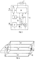
- FIG 1 shows the construction of the inventive active optical current measuring system 2, which consists of a sensor 4 and 6 sensor electronics.
- sensor 4 is A measuring resistor (shunt) is provided, which consists of two parts 8 and 10 exists. These parts 8 and 10 are end faces, respectively provided with a power rail 12 or 14. Moreover these shunt parts 8 and 10 are so designed that in assembled state of the shunt 4 a cavity 16 having. The sensor electronics 6 are in this cavity 16 arranged.
- the Shunt 4 practically forms the housing for the Sensor electronics 6, whose block diagram in Figure 2 in more detail is shown.
- the two parts 8 and 10 of the shunt 4 are made preferably made of manganine, whereas the power connection rails 12 and 14 are made of copper.
- the power connection rails 12 and 14 are with part 10 and 8, for example brazed. These power rails 12 and 14 serve on the one hand to connect the two shunt parts 8 and 10 and on the other hand for fastening in a busbar, for example a busbar of an intermediate circuit Large converter. To connect the two shunt parts 8 and 10, the power rails 12 and 14 with each other screwed or riveted together or welded together.
- the sensor 4 is also with two fiber optic connections provided that not in this representation are illustrated in more detail.
- the two optical fibers 18 and 20 are plugged in, the optical fiber 18 for transmission of the data stream or the mixed signal, consisting of a PWM signal and a data signal, and the optical waveguide 20 for the transmission of energy for the sensor electronics 6 responsible is.
- This structure of the active optical current measuring system ensures the mechanical protection of the sensor electronics 6 and prevents high-frequency interference on the Sensor electronics 6 can act because the shunt 4 as electromagnetic Shielding works.
- FIG. 2 shows the block diagram of the sensor electronics 6 shown in more detail.
- This sensor electronics 6 consists of a Energy converter 22, a measuring unit 24, processing electronics 26 and a digital mixing device 28.
- the measuring unit 24, which is used to regulate the supply voltage serves the processing electronics 26, has a reference value transmitter 30, a voltage divider 32, a comparator 34 and a PWM modulator 36.
- the Optical fiber 20 receives energy in the form of laser light to the energy converter 22, which in again this light converts electrical energy.
- the energy converter 22 built-up voltage is used directly, i.e. without additional Voltage regulation on site, to power the Processing electronics 26, the input side with the sensor 4 is linked. So that the supply voltage of the Processing electronics 26 can be kept constant this voltage is measured and with a reference voltage compared.
- the difference is pulse width modulated and with Using the mixing device 28, in particular a multiplexer, together with that of the processing electronics 26 data stream supplied to the evaluation electronics of the interface module transferred to earth potential. There will be actual measurement signal and the PWM signal separated again. While the measurement signal is being forwarded to a processor, the PWM signal is applied to a controller as an input signal, which changes the power of the transmitter so that the Voltage that the energy converter 22 builds up is kept constant becomes.
- the actual sensor signals are on the inside 38 of the shunt 4 tapped. Due to the mechanical structure the voltage drop across a shunt 4 is always only between two spatially relatively far apart points A and C tapped ( Figure 3).
- This line 40 is insulated closely on the inside 38 of shunt 4 misplaced.
- This line 40 is used to Point A applied to the shunt with low inductance to one Point B to be transferred.
- the measuring point B is spatially close to the measuring point C arranged. Between these two points B and C the actual sensor signal can be tapped and the Sensor electronics 6 are supplied.
- this interference compensation is linked to a condition because an interference field that the outer conductor loop penetrates and induces a current in it, penetrates also the measuring conductor loop and also induces one Circular current in this conductor loop.
- a full compensation the external interference field therefore only arises if the ratio of the partial resistances of the conductor loop and the measuring conductor loop are the same. In this case only are the voltage drops caused by the induced currents in the outer conductor loop (inside 38 of the Shunts) and the measuring loop and cancel each other out.
- the processing electronics 26 which consists of an input Amplifier circuit and an analog-digital converter on the output side exists, is designed so that an electronic Offset and gain adjustment is made possible.
- the shunt 4 can be manufactured first, the sensor electronics 6 used and the active optical current measuring system 2 can be adjusted without mechanical processing.
- the processing electronics 26 electronically controllable potentiometers.
- the respective The grinder position is saved at the end of the adjustment. When you switch on, the saved wiper position automatically read out again and the potentiometer adjusted.
- the transmission of the signals for adjusting the potentiometer can be both via a plug connection attached to the shunt take place as well in that the energy converter 22nd received light is modulated and the information in the Sensor electronics 6 is recovered. The comparison leaves perform themselves fully automatically.
Landscapes
- Physics & Mathematics (AREA)
- General Physics & Mathematics (AREA)
- Measuring Instrument Details And Bridges, And Automatic Balancing Devices (AREA)
Description
Die Erfindung bezieht sich auf ein aktives optisches Strommeßsystem.The invention relates to an active optical current measuring system.
Die Zwischenkreisspannungen in Großstromrichtern liegen heute bereits bei ca. 5 kV mit der Tendenz hin zu 10 kV und 20 kV. Derartig hohe Zwischenkreisspannungen stellen auch hohe Anforderungen an die Isolationsfestigkeit der verwendeten Strom- und Spannungswandler. Die Teilentladungsfestigkeit ist dabei die entscheidende Bemessungsgröße für die Isolationsfestigkeit. Bei 5 kV Zwischenkreisspannung muß eine Teilentladungsfestigkeit von 20 kV gefordert werden.The intermediate circuit voltages in large converters are today already at approx. 5 kV with a tendency towards 10 kV and 20 kV. Such high DC link voltages also make high demands the insulation strength of the used Current and voltage transformers. The partial discharge resistance is the decisive dimension for the insulation strength. At 5 kV intermediate circuit voltage, a partial discharge resistance is required of 20 kV are required.
Die heute verwendeten Wandlersysteme sind kompensierende Stromwandler. Zur Einhaltung der geforderten Teilentladungsfestigkeit müssen diese Wandler jedoch spezielle Herstellungsprozesse durchlaufen, die die Wandler sehr verteuern. Dazu kommt, daß diese Wandler einen großen Bauraum beanspruchen und die Leitungen zur Stromversorgung des Wandlers sowie zur Übertragung der Meßsignale unter Einhaltung der vorgeschriebenen Luft- und Kriechstrecken verlegt werden müssen, um eine sichere Trennung zu garantieren. Dadurch vergrößert sich der notwendige Bauraum weiter.The converter systems used today are compensatory Power converter. To maintain the required partial discharge resistance however, these converters have special manufacturing processes go through, which make the converters very expensive. In addition, these converters take up a large amount of space and the lines for powering the converter as well for the transmission of the measurement signals in compliance with the prescribed Clearances and creepage distances have to be laid, to guarantee a safe separation. This enlarges the necessary installation space.
Da die Wandler bereits eine Teilentladungsfestigkeit von 20 kV bei einer Zwischenkreisspannung von 5 kV kaum mehr garantieren können, scheint eine immer aufwendigere Isolation nicht der geeignete Weg zu sein, um die Wandlersysteme für noch höhere Zwischenkreisspannungen bei einem gleichzeitig niedrigen Preisniveau zu ertüchtigen. Since the converters already have a partial discharge resistance of 20 kV with an intermediate circuit voltage of 5 kV can hardly be guaranteed isolation seems increasingly complex not the appropriate way to convert the converter systems for even higher DC link voltages at the same time low price level.
Ein grundsätzlich anderer Ansatz zur Lösung dieses Problems ist, die sichere Trennung mittels Lichtleiter durchzuführen. Das bedeutet allerdings, daß sensorseitig eine Elektronik notwendig ist, die zumindest die vom Sensor gelieferten Meßsignale verstärkt und einen Lichtleitersender ansteuert. Die Energieversorgung dieser Elektronik muß dann aber ebenfalls über einen Lichtleiter erfolgen. Derartige Energieübertragungssysteme bestehen aus einem Laser, dem Lichtwellenleiter und einem Energiekonverter. Die übertragbare Leistung ist allerdings auf einige 100 mW beschränkt. Aus diesem Grunde kann in solchen lichtenergieversorgten Systemen kein kompensierender Stromwandler eingesetzt werden, da der Leistungsbedarf dieser Wandler aufgrund des Kompensationsstromes zu groß ist.A fundamentally different approach to solving this problem is to carry out the safe separation using a light guide. However, this means that electronics on the sensor side is necessary, at least the measurement signals supplied by the sensor amplified and controls an optical fiber transmitter. The Power supply for this electronics must then also be used via an optical fiber. Such energy transmission systems consist of a laser, the optical fiber and an energy converter. The transferable power is, however limited to a few 100 mW. Because of this, can in such systems supplied with light energy no compensation Current transformers are used because of the power requirement this converter is too large due to the compensation current.
Aus dem Aufsatz "Optische Stromwandler - erster Feldversuch
im 380-kV-Netz erfolgreich", abgedruckt in der DE-Zeitschrift
"ABB Technik", Band 3, 1994, Seiten 12 bis 18, ist ein aktives
optisches Strommeßsystem bekannt. Dieser Aufsatz stellt
verschiedene optische Stromwandler vor, die unter realen Bedingungen
in einem deutschen 380 kV-Netz getestet wurden. Der
aktive Stromwandler arbeitet im wesentlichen nach dem Prinzip
einer konventionellen Strommessung, ergänzt durch eine digitale
optische Übertragungsstrecke. Im einzelnen besteht das
System aus einer Luftkernspule einschließlich Bürde, einem
Analog-Digital-Wandler und einer Sendeeinheit mit lichtemittierender
Diode auf hohem Potential. Ein Lichtwellenleiter
stellt die Verbindung zum Schnittstellengerät auf Erdpotiental
her. Die Elektronik auf hohem Spannungspotential, als
Niederenergie CMOS-Schaltung aufgebaut, hat weniger als
150 µW Leistungsbedarf. Als Energieversorgung genügt eine Laserdiode,
die zwischen zwei Datentelegrammen über den gleichen
Lichtwellenleiter Energie sendet. Bei größeren Entfernungen
zwischen Sensor und Schnittstellengerät wird wegen der
höheren Sendeleistung ein paralleler Lichtwellenleiter zur
Energieversorgung benötigt. From the article "Optical current transformers - first field trial
successful in the 380 kV network ", printed in the DE magazine
"ABB Technik", volume 3, 1994,
Im Aufsatz "EHV Series Capacitor Banks. A New Approach To Platform To Ground Signalling, Relay Protection and Supervision", abgedruckt in der Zeitschrift IEEE Transactions on Power Delivery, Vol. 4, No. 2, April 1989, Seiten 1369 bis 1378, wird die Verwendung des vorgestellten aktiven Stromwandlers bei einem Serienkompensator beschrieben. Diesem Aufsatz ist neben dem Aufbau des aktiven Stromwandlers auch der Aufbau der Sensorelektronik und des Schnittstellengerätes auf Erdpotential zu entnehmen. Die Sensorelektronik besteht aus einem Filter, mehreren Spannungsteilern und einem Energiekonverter. Das Schnittstellengerät besteht aus einem Empfänger, einer Grenzwertschaltung, einem Detektor, einem Puffer und aus einem Pulsgenerator, einem Sender und einer Lichtweiche. Da der aktive Stromwandler zur Strommessung eine Luftkernspule mit Bürde verwendet, können mit diesem aktiven Stromwandler nur Wechselströme erfaßt werden.In the essay "EHV Series Capacitor Banks. A New Approach To Platform To Ground Signaling, Relay Protection and Supervision ", printed in the magazine IEEE Transactions on Power Delivery, Vol. 4, No. 2, April 1989, pages 1369 to 1378, the use of the active current transformer presented described in a series compensator. This essay is in addition to the construction of the active current transformer Structure of the sensor electronics and the interface device Take ground potential. The sensor electronics consists of a filter, several voltage dividers and an energy converter. The interface device consists of a receiver, a limit switch, a detector, a buffer and from a pulse generator, a transmitter and a light switch. Because the active current transformer for current measurement is an air core coil used with burden, can with this active current transformer only alternating currents are detected.
Ein Stromsensor, der auch Gleichströme erfassen kann und selbst keine Energieversorgung benötigt, ist ein Meßwiderstand oder Shunt.A current sensor that can also detect direct currents and A measuring resistor is itself not required for energy supply or shunt.
Aus der US-PS 4,070,572 ist ein Strommeßsystem bekannt, das einen Shunt, eine Sendeelektronik, eine Empfängerelektronik und eine Stromversorgungseinrichtung aufweist. Der Shunt ist in einer Hochspannungs-Wechselstromleitung angeordnet. Die Sendeelektronik ist eingangsseitig mit den Enden dieses Shunts verbunden und in unmittelbarer Nähe dieses Shunts angeordent. Die Stromversorgungseinrichtung koppelt aus der Hochspannungs-Wechselstromleitung Energie für die Sendeeinrichtung aus. Mittels eines Lichtwellenleiters gelangt das analoge Meßsignal zur Empfangseinrichtung auf Endpotential.A current measuring system is known from US Pat. No. 4,070,572 a shunt, transmitter electronics, receiver electronics and has a power supply device. The shunt is arranged in a high voltage AC line. The Transmitter electronics is on the input side with the ends of this Connected shunts and arranged in the immediate vicinity of this shunt. The power supply device couples out of the High voltage AC power line energy for the transmitter out. This is achieved using an optical fiber Analog measurement signal to the receiving device at end potential.
Da die Meßsignale des Shunts im Interesse einer niedrigen Verlustleistung klein gehalten werden müssen, sollte eine Sensorelektronik in unmittelbarer Umgebung des Shunts angeordnet werden, um Störungen weitgehend auszuschließen. Der Betrieb dieser Elektronik findet dann in elektromagnetisch rauher Umgebung statt, das heißt, sie wird von starken und unter Umständen schnell veränderlichen elektrischen und magnetischen Feldern beaufschlagt. Daneben ist die Elektronik in der Regel relativ hohen Temperaturen ausgesetzt. Ein Nachteil des Meßwiderstandes besteht darin, daß dieser für einen Abgleich mechanisch bearbeitet werden muß.Since the measurement signals of the shunt in the interest of a low Power dissipation should be kept low, one should Sensor electronics arranged in the immediate vicinity of the shunt in order to largely rule out interference. The Operation of this electronics then takes place in electromagnetic harsh environment instead, that is, it is characterized by strong and possibly rapidly changing electrical and magnetic Fields. In addition, the electronics are in usually exposed to relatively high temperatures. A disadvantage of the measuring resistor is that it is used for an adjustment must be machined.
Aus der WO 92/13277 ist ein Stromwandler zur Messung von Über- oder Kurzschlußströmen in einer gasisolierten, metallgekapselten Schaltanlage mit mindestens einem auf Hochspannungspotential befindlichen Leiter bekannt. Dieser Leiter wird mittels eines scheibenförmigen Stützisolators zwischen der Außenkapselung gehalten. der Leiter auf Hochspannungspotential ist rohrförmig ausgestaltet. Um diesen Leiter ist der Stromwandler herum angeordnet. Dazu weist der Leiter eine am Außenumfang umlaufende Vertiefung auf, die von dem Rohrstück des Stromwandlers, dessen Außendurchmesser dem Außendurchmesser des Innenleiters gleicht, abgedeckt wird. Die Länge dieses dünnwandigen Rohrstückes richtet sich nach der gewünschten Strommeßempfindlichkeit. Der Spannungsabfall über dem Rohrstück wird durch Leitungen der Anschlußleiter abgegriffen und einer im Inneren des Innenleiters befindlichen Wandlerschaltungsanordnung zugeführt. Der zwischen dem dünnwandigen Rohrstück und dem Boden der Vertiefung (Nut) befindliche Innenraum kann mit einem festen Isolierstoff ausgefüllt werden. Außerdem richtet sich die Tiefe dieser Vertiefung nach der Frequenz des zu messenden transienten Kurzschlußstromes. Je höher die Frequenz, desto kleiner die Tiefe dieser Vertiefung.WO 92/13277 describes a current transformer for measuring Overcurrent or short-circuit currents in a gas-insulated, metal-enclosed Switchgear with at least one on high voltage potential located leader known. That leader is between by means of a disc-shaped support insulator the outer encapsulation held. the conductor at high voltage potential is tubular. Around this leader is the Current transformers arranged around. To this end, the leader has an am Outer circumferential recess on that of the pipe section of the current transformer, the outside diameter of which is the outside diameter of the inner conductor is covered. The length this thin-walled piece of pipe depends on the desired Current measurement sensitivity. The voltage drop across the Pipe piece is tapped through lines of the connecting conductors and a converter circuit arrangement located inside the inner conductor fed. The one between the thin-walled Pipe piece and the bottom of the recess (groove) located interior can be filled with a solid insulating material. In addition, the depth of this depression depends on the Frequency of the transient short-circuit current to be measured. Each the higher the frequency, the smaller the depth of this depression.
Der Erfindung liegt nun die Aufgabe zugrunde, ein aktives optisches Strommeßsystem anzugeben, mit dem auch Gleichströme erfaßt werden können und dessen Sensorelektronik gegen Störungen geschützt ist.The invention is based on the object, an active specify optical current measuring system with which also direct currents can be detected and its sensor electronics against interference is protected.
Diese Aufgabe wird erfindungsgemäß gelöst mit den Merkmalen des Anspruchs 1.This object is achieved with the features of claim 1.
Dadurch, daß der Sensor aus zwei Teilen besteht, die im zusammengesetzten Zustand einen Hohlraum aufweisen, in dem die Sensorelektronik untergebracht ist, und als Sensor einen Meßwiderstand vorgesehen ist, bildet dieser Meßwiderstand (Shunt) das Gehäuse für die Sensorelektronik. Dieser Aufbau gewährleistet den mechanischen Schutz der Elektronik und verhindert, daß hochfrequente Störungen auf die Elektronik einwirken können, da der Shunt als elektromagnetische Abschirmung wirkt. Die eigentlichen Sensorsignale werden an der Innenseite des Shunts abgegriffen.Because the sensor consists of two parts, the assembled State have a cavity in which the Sensor electronics is housed, and as a sensor a measuring resistor is provided, this measuring resistor forms (Shunt) the housing for the sensor electronics. This structure ensures the mechanical protection of the electronics and prevents that high-frequency interference affect the electronics can, as the shunt acts as an electromagnetic shield works. The actual sensor signals are on the inside tapped from the shunt.
Bei einer vorteilhaften Ausführungsform des aktiven optischen Strommeßsystems ist die Sensorelektronik im Inneren des Shunts eingangsseitig mit zwei räumlich dicht beieinanderliegenden Meßpunkten verknüpft, wobei der erste Meßpunkt ein Punkt der Innenseite des Sensors ist und der zweite Meßpunkt mittels einer entlang der Innenseite des Sensors isoliert geführten Leitung mit einem weiteren Punkt der Innenseite des Sensors verbunden ist, wobei dieser weitere Punkt derart gewählt ist, daß der zweite Meßpunkt und dieser weitere Meßpunkt räumlich relativ weit auseinanderliegen. Mittels dieser isoliert geführten Leitung wird das am weiteren Punkt anliegende Potential am Shunt niederinduktiv an den zweiten Meßpunkt übertragen. Auf diese Art und Weise erhält man als Meßspannung immer genau die Spannung, die dem durch den Strom hervorgerufenen Spannungsabfall an der geschlossenen Leiterschleife entlang des Weges der Meßleitung entspricht. In an advantageous embodiment of the active optical Current measuring system is the sensor electronics inside the Shunts on the input side with two spatially close to each other Measurement points linked, the first measurement point being a Point is the inside of the sensor and the second measurement point by means of an insulated led along the inside of the sensor Line with another point on the inside of the Sensor is connected, with this further point selected in this way is that the second measuring point and this further measuring point spatially relatively far apart. By means of this The line that is routed in isolation becomes the one at the other point Low-inductance potential at the second measuring point transfer. In this way one obtains the measuring voltage always exactly the voltage caused by the current caused voltage drop at the closed conductor loop along the path of the measuring line.
Bei einer besonders vorteilhaften Ausführungsform ist der zweite Meßpunkt mittels mehrerer entlang der Innenseite des Sensors isoliert geführter Leitungen mit dem weiteren Punkt der Innenseite des Sensors verbunden, die einen Käfig bilden. Durch diese Ausgestaltung der mehreren Meßleitungen zu einem Käfig wird die Störsicherheit gegenüber äußeren Störfeldern wesentlich erhöht.In a particularly advantageous embodiment, the second measuring point by means of several along the inside of the Sensor insulated cables with the further point connected to the inside of the sensor, which form a cage. This configuration of the several measuring lines into one The cage becomes immunity to interference from external interference fields significantly increased.
Bei einer weiteren vorteilhaften Ausführungsform weist die Sensorelektronik elektronisch steuerbare Potentiometer auf. Dadurch wird ein elektronischer Offset- und Verstärkungsabgleich ermöglicht. Dadurch kann der Shunt zunächst gefertigt, die Elektronik eingesetzt und das Strommeßsystem ohne mechanische Bearbeitung abgeglichen werden. Die jeweiligen Schleifenpositionen der elektronisch steuerbaren Potentiometer werden abgespeichert. Beim Einschalten des aktiven optischen Strommeßsystems wird die gespeicherte Position automatisch wieder ausgelesen und die Potentiometer werden justiert.In a further advantageous embodiment, the Sensor electronics electronically controllable potentiometers. This makes an electronic offset and gain adjustment enables. This allows the shunt to be manufactured the electronics used and the current measuring system without mechanical Processing. The respective loop positions the electronically controllable potentiometer saved. When you turn on the active optical Current measurement system, the stored position is automatically read out again and the potentiometers are adjusted.
Der Abgleich dieses Strommeßsystems erfolgt hinsichtlich Nullpunkt und Verstärkung bzw. Übertragungsbeiwert. Die Übertragung der Signale zum Verstellen der elektronisch steuerbaren Potentiometer können sowohl über einem Shunt angebrachte Steckverbindung erfolgen als auch dadurch, daß das vom Sender der Auswerteelektronik auf Erdpotential gesendete Licht moduliert und die Information auf der Sensorelektronik zurückgewonnen wird. Der Abgleich läßt sich vollautomatisch durchführen.This current measuring system is compared in terms of Zero point and gain or transmission coefficient. The transfer of the signals for adjusting the electronically controllable Potentiometers can both be mounted over a shunt Plug connection take place as well in that the from Transmitter of the evaluation electronics sent to earth potential Light modulates and the information on the sensor electronics is recovered. The adjustment can be done fully automatically carry out.
Zur weiteren Erläuterung der Erfindung wird auf die Zeichnung Bezug genommen, in der ein Ausführungsbeispiel des aktiven optischen Strommeßsystems schematisch veranschaulicht ist.
- Figur 1
- zeigt den konstruktiven Aufbau des erfindungsgemäßen Strommeßsystems, die
Figur 2- zeigt das Blockschaltbild der Sensorelektronik des Strommeßsystems nach Figur 1, in
- Figur 3
- ist die Ermittlung des Sensorsignals dargestellt und die
Figur 4- veranschaulicht den vereinfachten Kompensationskäfig.
- Figure 1
- shows the construction of the current measuring system according to the invention, the
- Figure 2
- shows the block diagram of the sensor electronics of the current measuring system according to Figure 1, in
- Figure 3
- the determination of the sensor signal is shown and the
- Figure 4
- illustrates the simplified compensation cage.
Die Figur 1 zeigt den konstruktiven Aufbau des erfindungsgemaßen
aktiven optischen Strommeßsystems 2, der aus einem Sensor
4 und einer Sensorelektronik 6 besteht. Als Sensor 4 ist
ein Meßwiderstand (Shunt) vorgesehen, der aus zwei Teilen 8
und 10 besteht. Diese Teile 8 und 10 sind stirnseitig jeweils
mit einer Strom-Anschlußschiene 12 bzw. 14 versehen. Außerdem
sind diese Shuntteile 8 und 10 dermaßen ausgebildet, daß im
zusammengebauten Zustand der Shunt 4 einen Hohlraum 16
aufweist. In diesem Hohlraum 16 ist die Sensorelektronik 6
angeordnet. Der Shunt 4 bildet praktisch das Gehäuse für die
Sensorelektronik 6, deren Blockschaltbild in Figur 2 näher
dargestellt ist. Die beiden Teile 8 und 10 des Shunts 4 bestehen
vorzugsweise aus Manganin, wogegen die Strom-Anschlußschienen
12 und 14 aus Kupfer bestehen. Die Strom-Anschlußschienen
12 bzw. 14 sind mit dem Teil 10 bzw. 8 beispielsweise
hartverlötet. Diese Strom-Anschlußschienen 12 und 14
dienen einerseits zur Verbindung der beiden Shuntteile 8 und
10 und andererseits zur Befestigung in einer Stromschiene,
beispielsweise einer Stromschiene eines Zwischenkreises eines
Großstromrichters. Zur Verbindung der beiden Shuntteile 8 und
10 werden die Strom-Anschlußschienen 12 und 14 miteinander
verschraubt oder miteinander vernietet oder miteinander verschweißt.
Der Sensor 4 ist außerdem mit zwei Lichtwellenleiter-Anschlüssen
versehen, die bei dieser Darstellung nicht
näher veranschaulicht sind. In diese Lichtwellenleiter-Anschlüsse
werden die beiden Lichtwellenleiter 18 und 20 gesteckt,
wobei der Lichtwellenleiter 18 für die Übertragung
des Datenstromes bzw. des Mischsignals, bestehend aus einem
PWM-Signal und einem Datensignal, und der Lichtwellenieiter
20 für die Übertragung der Energie für die Sensorelektronik 6
zuständig ist. Dieser Aufbau des aktiven optischen Strommeßsystems
gewährleistet den mechanischen Schutz der Sensorelektronik
6 und verhindert, daß hochfrequente Störungen auf die
Sensorelektronik 6 einwirken können, da der Shunt 4 als elektromagnetische
Abschirmung wirkt.Figure 1 shows the construction of the inventive
active optical
In der Figur 2 ist das Blockschaltbild der Sensorelektronik 6
näher dargestellt. Diese Sensorelektronik 6 besteht aus einem
Energiekonverter 22, einer Meßeinheit 24, einer Verarbeitungselektronik
26 und einer digitalen Mischeinrichtung 28.
Die Meßeinheit 24, die zur Regelung der Versorgungsspannung
der Verarbeitungselektronik 26 dient, weist einen Referenzwertgeber
30, einen Spannungsteiler 32, einen Vergleicher 34
und einen PWM-Modulator 36 auf. Mittels des
Lichtwellenleiters 20 gelangt Energie in Form von Laserlicht
zum Energiekonverter 22, der dieses Licht wieder in
elektrische Energie umwandelt. Die vom Energiekonverter 22
aufgebaute Spannung dient direkt, also ohne zusätzliche
Spannungsregelung vor Ort, zur Stromversorgung der
Verarbeitungselektronik 26, die eingangsseitig mit dem Sensor
4 verknüpft ist. Damit dennoch die Versorgungs-spannung der
Verarbeitungselektronik 26 konstant gehalten werden kann,
wird diese Spannung gemessen und mit einer Referenzspannung
verglichen. Die Differenz wird pulsbreiten-moduliert und mit
Hilfe der Mischeinrichtung 28, insbesondere einem Multiplexer,
zusammen mit dem von der Verarbeitungselektronik 26
gelieferten Datenstrom an die Auswerteelektronik der Schnittstellenbaugruppe
auf Erdpotential übertragen. Dort werden das
eigentliche Meßsignal und das PWM-Signal wieder getrennt.
Während das Meßsignal an einen Prozessor weitergeleitet wird,
wird das PWM-Signal als Eingangssignal an einen Regler gelegt,
der die Leistung des Senders so verändert, daß die
Spannung, die der Energiekonverter 22 aufbaut, konstant gehalten
wird. FIG. 2 shows the block diagram of the
Eine genaue Beschreibung dieser Sensorelektronik 6 und deren
Funktionsweise ist einer parallel eingereichten deutschen
Patentanmeldung mit dem amtlichen Aktenzeichen 195 10 660.1
zu entnehmen.A detailed description of this
Die eigentlichen Sensorsignale werden an der Innenseite 38
des Shunts 4 abgegriffen. Aufgrund des mechanischen Aufbaus
ist der Spannungsabfall über einen Shunt 4 immer nur zwischen
zwei räumlich relativ weit auseinanderliegenden Punkten A und
C abgreifbar (Figur 3). Um die Meßspannung in einer Elektronik
6, in dieser Darstellung wegen der Übersichtlichkeit
nicht näher dargestellt, verarbeiten zu können, muß die Meßspannung
aber einem Verstärker zugeführt werden, dessen Anschlüsse
im allgemeinen räumlich dicht beieinander liegen.
Somit muß die Meßspannung über eine Leitung 40 geführt werden.
Diese Leitung 40 ist isoliert eng an der Innenseite 38
des Shunts 4 verlegt. Diese Leitung 40 dient dazu, das am
Punkt A anliegende Potential am Shunt niederinduktiv an einen
Punkt B zu übertragen. Der Meßpunkt B ist räumlich dicht bei
dem Meßpunkt C angeordnet. Zwischen diesen beiden Punkten B
und C kann das eigentliche Sensorsignal abgegriffen und der
Sensorelektronik 6 zugeführt werden.The actual sensor signals are on the inside 38
of the
Zur Vermeidung eines Störeinflusses muß sichergestellt werden,
daß zwischen der geschlossenen Leiterschleife (Innenseite
38 des Shunts 4) und der Meßleitung 40 keine offene Leiterschleife
existiert. Diese Bedingung läßt sich nur durch
eine geschlossene Meßleiterschleife erfüllen, die praktisch
deckungsgleich mit der ersten Leiterschleife ist, aber isoliert
von dieser. Lediglich am Punkt A sind beide Leiterschleifen
miteinander verbunden.To avoid interference, it must be ensured that
that between the closed conductor loop (inside
38 of the shunt 4) and the measuring
Allerdings ist diese Störkompensation an eine Bedingung geknüpft, denn ein Störfeld, das die äußere Leiterschleife durchsetzt und in dieser einen Strom induziert, durchdringt auch die Meßleiterschleife und induziert ebenfalls einen Kreisstrom in dieser Leiterschleife. Eine vollständige Kompensation des äußeren Störfeldes ergibt sich deshalb nur, wenn das Verhältnis der Teilwiderstände der Leiterschleife und der Meßleiterschleife gleich sind. Nur in diesem Fall sind die durch die induzierten Ströme hervorgerufenen Spannungsabfälle in der äußeren Leiterschleife (Innenseite 38 des Shunts) und der Meßleiterschleife gleich und heben sich auf.However, this interference compensation is linked to a condition because an interference field that the outer conductor loop penetrates and induces a current in it, penetrates also the measuring conductor loop and also induces one Circular current in this conductor loop. A full compensation the external interference field therefore only arises if the ratio of the partial resistances of the conductor loop and the measuring conductor loop are the same. In this case only are the voltage drops caused by the induced currents in the outer conductor loop (inside 38 of the Shunts) and the measuring loop and cancel each other out.
Damit man eine Meßleiterschleife erhält, muß eine weitere
Meßleitung 40 vorgesehen sein, die im Punkt A mit der ersten
Meßleitung 40 und mit dem Shunt 4 und mit der ersten Meßleitung
40 am Punkt B verbunden ist (Figur 4). Da der Shunt 4
dreidimensional ist, können die Störfelder in jeder Raumrichtung
auf den Shunt 4 einwirken und entsprechende Wirbelströme
induzieren. Die Meßleiterschleife muß deshalb ebenfalls dreidimensional
gestaltet sein. Diese nimmt nun die Form eines
Käfigs 42 an gemäß Figur 4, der sich an der Innenseite 38 des
Shunts anschmiegt, aber von diesem isoliert ist. Im Idealfall
bildet der Käfig 42 ein geschlossenes Gehäuse. Bereits mit
einem symmetrischen, aus nur sechs Einzelleitern 40 bestehenden
Käfig 42 wird eine Störkompensation von ca. 90% gegenüber
einer einzigen Leiterschleife erreicht. Wie in Figur 4 angedeutet
ist, verlaufen die einzelnen Leiter 40 des Käfigs 42
in Richtung des äußeren Stromflusses. Zwar können dadurch
keine Wirbelströme quer zur Stromflußrichtung kompensiert
werden, diese tragen aber in erster Näherung nicht zu einer
Verfälschung der Meßspannung des Shunts 4 bei.In order to get a measuring conductor loop, another one
Die Verarbeitungselektronik 26, die aus einer eingangsseitigen
Verstärkerschaltung und einem ausgangsseitigen Analog-Digital-Wandler
besteht, ist so gestaltet, daß ein elektronischer
Offset- und Verstärkungsabgleich ermöglicht wird. Dadurch
kann der Shunt 4 zunächst gefertigt werden, die Sensorelektronik
6 eingesetzt und das aktive optische Strommeßsystem
2 ohne mechanische Bearbeitung abgeglichen werden. Für
den elektronischen Abgleich des Strommeßsystems 2 befinden
sich in der Verstärkerschaltung der Verarbeitungselektronik
26 elektronisch steuerbare Potentiometer. Die jeweilige
Schleiferposition wird am Ende des Abgleichs abgespeichert.
Beim Einschalten wird die gespeicherte Schleiferposition
automatisch wieder ausgelesen und das Potentiometer justiert.
Die Übertragung der Signale zum Verstellen der Potentiometer
kann sowohl über eine am Shunt angebrachte Steckverbindung
erfolgen als auch dadurch, daß das vom Energiekonverter 22
empfangene Licht moduliert ist und die Information in der
Sensorelektronik 6 zurückgewonnen wird. Der Abgleich läßt
sich vollautomatisch durchführen.The
Claims (10)
- Active optical current measuring system (2) consisting of a sensor (4) provided with current terminal rails (12, 14) and an optical waveguide terminal, the said sensor consisting of two parts (8, 10) which when assembled form a cavity (16), and an electronic sensor circuit (6) fitted in this cavity (16) with its output end connected to the optical waveguide terminal, whereby the sensor (4) is a measuring resistor.
- Active optical current measuring system (2) in accordance with claim 1, whereby the input end of the electronic sensor circuit (6) fitted in the cavity (16) is connected to two measuring points (C, B) positioned spatially close together, at which a measuring voltage can be tapped off, whereby the first measuring point (C) is a point on the inside (38) of the sensor (4) and the second measuring point (B) is connected by a lead (40) passing, insulated, along the inside (38) of the sensor (4) to a further point (A) of the inside (38) of the sensor (4), whereby this further point (A) is chosen so that the second measuring point (B) and the further point (A) are spatially relatively far apart.
- Active optical current measuring system (2) in accordance with claim 2, whereby the second measuring point (B) is connected by means of several insulated leads (40) passing along the inside (38) of the sensor (4) to the further point (A) of the inside (38) of the sensor (4).
- Active optical current measuring system (2) in accordance with claim 3, whereby the several leads (40) run in the direction of the current to be measured flowing through the sensor (4) and form a cage (42).
- Active optical current measuring system (2) in accordance with claim 4, whereby the cage (42) form a closed housing.
- Active optical current measuring system (2) in accordance with claim 1, whereby the electronic sensor circuit (6) has electronically controlled potentiometers for its electronic calibration.
- Active optical current measuring system (2) in accordance with claim 1, whereby the parts (8, 10) of the sensor (4) are each provided with a current terminal rail (12, 14).
- Active optical current measuring system (2) in accordance with claim 1, whereby the sensor (4) is made of manganese.
- Active optical current measuring system (2) in accordance with claim 7, whereby the current terminal rails (12, 14) are made of copper.
- Active optical current measuring system (2) in accordance with claim 1, whereby the sensor (4) is provided with a further optical waveguide terminal.
Applications Claiming Priority (3)
| Application Number | Priority Date | Filing Date | Title |
|---|---|---|---|
| DE19510662A DE19510662C2 (en) | 1995-03-23 | 1995-03-23 | Active optical current measuring system |
| DE19510662 | 1995-03-23 | ||
| PCT/DE1996/000358 WO1996029608A1 (en) | 1995-03-23 | 1996-02-29 | Active optical current measuring system |
Publications (2)
| Publication Number | Publication Date |
|---|---|
| EP0815455A1 EP0815455A1 (en) | 1998-01-07 |
| EP0815455B1 true EP0815455B1 (en) | 2001-05-02 |
Family
ID=7757521
Family Applications (1)
| Application Number | Title | Priority Date | Filing Date |
|---|---|---|---|
| EP96905675A Expired - Lifetime EP0815455B1 (en) | 1995-03-23 | 1996-02-29 | Active optical current measuring system |
Country Status (4)
| Country | Link |
|---|---|
| US (1) | US6034521A (en) |
| EP (1) | EP0815455B1 (en) |
| DE (2) | DE19510662C2 (en) |
| WO (1) | WO1996029608A1 (en) |
Families Citing this family (27)
| Publication number | Priority date | Publication date | Assignee | Title |
|---|---|---|---|---|
| GB9813982D0 (en) * | 1998-06-30 | 1998-08-26 | Mem Limited | Residual current detection device |
| DE19854436A1 (en) * | 1998-11-25 | 2000-06-15 | Siemens Ag | Measurement arrangement for electric current in conductor |
| DE19906276A1 (en) * | 1999-02-15 | 2000-09-21 | Heusler Isabellenhuette | Method and current measuring module for current monitoring in a power supply system |
| US6826369B1 (en) * | 1999-04-23 | 2004-11-30 | System To Asic, Inc. | Intelligent sensor platform |
| GB0000067D0 (en) * | 2000-01-06 | 2000-02-23 | Delta Electrical Limited | Current detector and current measurement apparatus including such detector with temparature compensation |
| DE10047225C1 (en) * | 2000-09-23 | 2002-06-06 | Fraunhofer Ges Forschung | Electromagnetic field measuring device with transducer transmitting measured values to external evaluation device and conversion of received optical radiation into electrical operating energy |
| US20040036461A1 (en) * | 2002-08-22 | 2004-02-26 | Sutherland Peter Edward | Switchgear and relaying configuration |
| DE102004007851B4 (en) * | 2004-02-17 | 2006-03-16 | Kromberg & Schubert Gmbh & Co. Kg | Connection device for a battery |
| DE102004040575A1 (en) | 2004-08-21 | 2006-02-23 | Abb Patent Gmbh | Device for measuring electrical current, voltage and temperature on an electrical conductor made of rigid material |
| US7688022B2 (en) | 2006-02-17 | 2010-03-30 | Lear Corporation | Energy management system for a vehicle |
| US7598724B2 (en) * | 2007-01-19 | 2009-10-06 | Admmicro Properties, Llc | Flexible current transformer assembly |
| US8476864B2 (en) * | 2007-06-13 | 2013-07-02 | Lear Corporation | Battery monitoring system |
| DE102007036837A1 (en) * | 2007-08-02 | 2009-02-05 | Siemens Ag | Current measurement, at a low voltage switch, has a measurement resistance integrated into the current conductor with a measurement module on it |
| US8773255B2 (en) | 2007-09-24 | 2014-07-08 | Ppc Broadband, Inc. | Status sensing and reporting interface |
| US8570178B2 (en) * | 2007-09-24 | 2013-10-29 | Ppc Broadband, Inc. | Coaxial cable connector with internal floating ground circuitry and method of use thereof |
| US8305034B2 (en) * | 2008-07-23 | 2012-11-06 | Lear Corporation | Battery monitoring system |
| US8376774B2 (en) * | 2008-11-17 | 2013-02-19 | Rochester Institute Of Technology | Power extracting device and method of use thereof |
| US8419464B2 (en) * | 2008-11-17 | 2013-04-16 | Ppc Broadband, Inc. | Coaxial connector with integrated molded substrate and method of use thereof |
| US8414326B2 (en) * | 2008-11-17 | 2013-04-09 | Rochester Institute Of Technology | Internal coaxial cable connector integrated circuit and method of use thereof |
| US8618944B2 (en) * | 2009-12-03 | 2013-12-31 | Ppc Broadband, Inc. | Coaxial cable connector parameter monitoring system |
| US8604936B2 (en) | 2010-12-13 | 2013-12-10 | Ppc Broadband, Inc. | Coaxial cable connector, system and method of use thereof |
| DE102012213196A1 (en) | 2011-07-28 | 2013-01-31 | Continental Teves Ag & Co. Ohg | Circuit for conducting an electric current |
| EP2568296A1 (en) | 2011-09-12 | 2013-03-13 | Eaton Industries GmbH | Measuring resistance with short circuit protection |
| US9013189B2 (en) * | 2012-11-07 | 2015-04-21 | Eaton Corporation | Electrical joint monitoring device and electrical joint monitoring system employing the same |
| DE102016204949A1 (en) * | 2016-03-24 | 2017-09-28 | Continental Automotive Gmbh | battery sensor |
| EP3452838B1 (en) * | 2016-05-04 | 2023-02-22 | Safran Electrical & Power | Busbar current sensor assembly |
| EP3330720B1 (en) * | 2016-11-30 | 2019-06-26 | Yuyang DNU Co., Ltd | System for charge-discharge cycler |
Citations (1)
| Publication number | Priority date | Publication date | Assignee | Title |
|---|---|---|---|---|
| WO1992013277A1 (en) * | 1991-01-23 | 1992-08-06 | Abb Patent Gmbh | Current transformer |
Family Cites Families (4)
| Publication number | Priority date | Publication date | Assignee | Title |
|---|---|---|---|---|
| DE1939510C3 (en) * | 1969-07-31 | 1974-08-29 | Siemens Ag, 1000 Berlin Und 8000 Muenchen | Measuring device for currents in high voltage conductors |
| US4070572A (en) * | 1976-12-27 | 1978-01-24 | General Electric Company | Linear signal isolator and calibration circuit for electronic current transformer |
| CH630466A5 (en) * | 1978-08-31 | 1982-06-15 | Sprecher & Schuh Ag | Current measuring arrangement |
| US5461307A (en) * | 1994-03-03 | 1995-10-24 | General Electric Company | Electro-optical current sensing system and method for sensing and avoiding thermally induced measurement error therein |
-
1995
- 1995-03-23 DE DE19510662A patent/DE19510662C2/en not_active Expired - Fee Related
-
1996
- 1996-02-29 DE DE59606851T patent/DE59606851D1/en not_active Expired - Lifetime
- 1996-02-29 WO PCT/DE1996/000358 patent/WO1996029608A1/en active IP Right Grant
- 1996-02-29 EP EP96905675A patent/EP0815455B1/en not_active Expired - Lifetime
- 1996-02-29 US US08/913,738 patent/US6034521A/en not_active Expired - Fee Related
Patent Citations (1)
| Publication number | Priority date | Publication date | Assignee | Title |
|---|---|---|---|---|
| WO1992013277A1 (en) * | 1991-01-23 | 1992-08-06 | Abb Patent Gmbh | Current transformer |
Also Published As
| Publication number | Publication date |
|---|---|
| DE19510662A1 (en) | 1996-10-02 |
| US6034521A (en) | 2000-03-07 |
| DE59606851D1 (en) | 2001-06-07 |
| DE19510662C2 (en) | 1998-08-06 |
| EP0815455A1 (en) | 1998-01-07 |
| WO1996029608A1 (en) | 1996-09-26 |
Similar Documents
| Publication | Publication Date | Title |
|---|---|---|
| EP0815455B1 (en) | Active optical current measuring system | |
| DE69626431T2 (en) | Linear 2-way isolation circuit | |
| DE102006061923A1 (en) | Rogowski sensor and method for measuring a current | |
| DE19712900A1 (en) | Sensor system for measuring electric current and voltage esp. for medium voltage | |
| EP2555003B1 (en) | Current transducer and load separator with same | |
| EP0596566B1 (en) | High-voltage transformer | |
| EP0510427A2 (en) | Voltage transformer for a medium or high voltage installation | |
| DE4322944C2 (en) | Current transformer of an electrical switchgear filled with protective gas | |
| DE4133508C1 (en) | High voltage measurement transducer for gas insulated HV switchgear - has coil in recess of internal conductor having transmission circuit for conversion of digitised electrical signal to light signal | |
| DE4203725C2 (en) | Arrangement for electrically isolated capacitance measurement, especially for capacitive level measurement | |
| DE4101859C1 (en) | ||
| DE10258115B4 (en) | Broadband measuring module for current measurement at power electronics devices | |
| DE19854436A1 (en) | Measurement arrangement for electric current in conductor | |
| AT521644B1 (en) | Device for measuring current and voltage | |
| DE3708731C1 (en) | Electrical circuit arrangement for detecting noise pulses in high-voltage systems | |
| DE3912506A1 (en) | Partial discharge sensor for testing transformer or generator - has adaptor for each test object, complementary bipolar transistor input stage, and amplifies and stretches partial discharge signal | |
| DE19649304A1 (en) | Switching arrangement for isolated voltage and / or current measurement | |
| EP0723159A1 (en) | Current measuring device with measuring transducer | |
| AT399601B (en) | Current transformer for a high-voltage conductor | |
| DE641279C (en) | Arrangement for measuring earth resistance | |
| DE4406722C1 (en) | Line differential protection system with respective protection unit | |
| DE2151182C3 (en) | Device for measuring electrical current resistance | |
| EP0216037A1 (en) | Device for measuring the transient potential of the case of a metal encapsulated, gas-insulated high tension plant | |
| DE102022104394A1 (en) | Electrical protection device with measuring module | |
| DE19836082A1 (en) | Converter device for protective devices and circuit breaker devices |
Legal Events
| Date | Code | Title | Description |
|---|---|---|---|
| PUAI | Public reference made under article 153(3) epc to a published international application that has entered the european phase |
Free format text: ORIGINAL CODE: 0009012 |
|
| 17P | Request for examination filed |
Effective date: 19970918 |
|
| AK | Designated contracting states |
Kind code of ref document: A1 Designated state(s): DE FR GB IT |
|
| 17Q | First examination report despatched |
Effective date: 19981203 |
|
| GRAG | Despatch of communication of intention to grant |
Free format text: ORIGINAL CODE: EPIDOS AGRA |
|
| GRAG | Despatch of communication of intention to grant |
Free format text: ORIGINAL CODE: EPIDOS AGRA |
|
| GRAH | Despatch of communication of intention to grant a patent |
Free format text: ORIGINAL CODE: EPIDOS IGRA |
|
| GRAH | Despatch of communication of intention to grant a patent |
Free format text: ORIGINAL CODE: EPIDOS IGRA |
|
| GRAA | (expected) grant |
Free format text: ORIGINAL CODE: 0009210 |
|
| AK | Designated contracting states |
Kind code of ref document: B1 Designated state(s): DE FR GB IT |
|
| GBT | Gb: translation of ep patent filed (gb section 77(6)(a)/1977) |
Effective date: 20010502 |
|
| REF | Corresponds to: |
Ref document number: 59606851 Country of ref document: DE Date of ref document: 20010607 |
|
| ITF | It: translation for a ep patent filed |
Owner name: STUDIO JAUMANN P. & C. S.N.C. |
|
| ET | Fr: translation filed | ||
| REG | Reference to a national code |
Ref country code: GB Ref legal event code: IF02 |
|
| PLBE | No opposition filed within time limit |
Free format text: ORIGINAL CODE: 0009261 |
|
| STAA | Information on the status of an ep patent application or granted ep patent |
Free format text: STATUS: NO OPPOSITION FILED WITHIN TIME LIMIT |
|
| 26N | No opposition filed | ||
| PGFP | Annual fee paid to national office [announced via postgrant information from national office to epo] |
Ref country code: IT Payment date: 20090225 Year of fee payment: 14 |
|
| PGFP | Annual fee paid to national office [announced via postgrant information from national office to epo] |
Ref country code: GB Payment date: 20100212 Year of fee payment: 15 |
|
| PG25 | Lapsed in a contracting state [announced via postgrant information from national office to epo] |
Ref country code: IT Free format text: LAPSE BECAUSE OF NON-PAYMENT OF DUE FEES Effective date: 20100228 |
|
| GBPC | Gb: european patent ceased through non-payment of renewal fee |
Effective date: 20110228 |
|
| PG25 | Lapsed in a contracting state [announced via postgrant information from national office to epo] |
Ref country code: GB Free format text: LAPSE BECAUSE OF NON-PAYMENT OF DUE FEES Effective date: 20110228 |
|
| PGFP | Annual fee paid to national office [announced via postgrant information from national office to epo] |
Ref country code: FR Payment date: 20140212 Year of fee payment: 19 |
|
| PGFP | Annual fee paid to national office [announced via postgrant information from national office to epo] |
Ref country code: DE Payment date: 20140417 Year of fee payment: 19 |
|
| REG | Reference to a national code |
Ref country code: DE Ref legal event code: R119 Ref document number: 59606851 Country of ref document: DE |
|
| REG | Reference to a national code |
Ref country code: FR Ref legal event code: ST Effective date: 20151030 |
|
| PG25 | Lapsed in a contracting state [announced via postgrant information from national office to epo] |
Ref country code: DE Free format text: LAPSE BECAUSE OF NON-PAYMENT OF DUE FEES Effective date: 20150901 |
|
| PG25 | Lapsed in a contracting state [announced via postgrant information from national office to epo] |
Ref country code: FR Free format text: LAPSE BECAUSE OF NON-PAYMENT OF DUE FEES Effective date: 20150302 |