EP0735576A2 - Integrated circuit fabrication - Google Patents
Integrated circuit fabrication Download PDFInfo
- Publication number
- EP0735576A2 EP0735576A2 EP96302136A EP96302136A EP0735576A2 EP 0735576 A2 EP0735576 A2 EP 0735576A2 EP 96302136 A EP96302136 A EP 96302136A EP 96302136 A EP96302136 A EP 96302136A EP 0735576 A2 EP0735576 A2 EP 0735576A2
- Authority
- EP
- European Patent Office
- Prior art keywords
- layer
- bonding pads
- fuses
- silicon nitride
- pads
- Prior art date
- Legal status (The legal status is an assumption and is not a legal conclusion. Google has not performed a legal analysis and makes no representation as to the accuracy of the status listed.)
- Withdrawn
Links
Images


Classifications
-
- H—ELECTRICITY
- H01—ELECTRIC ELEMENTS
- H01L—SEMICONDUCTOR DEVICES NOT COVERED BY CLASS H10
- H01L21/00—Processes or apparatus adapted for the manufacture or treatment of semiconductor or solid state devices or of parts thereof
- H01L21/70—Manufacture or treatment of devices consisting of a plurality of solid state components formed in or on a common substrate or of parts thereof; Manufacture of integrated circuit devices or of parts thereof
- H01L21/71—Manufacture of specific parts of devices defined in group H01L21/70
- H01L21/768—Applying interconnections to be used for carrying current between separate components within a device comprising conductors and dielectrics
- H01L21/76838—Applying interconnections to be used for carrying current between separate components within a device comprising conductors and dielectrics characterised by the formation and the after-treatment of the conductors
- H01L21/76886—Modifying permanently or temporarily the pattern or the conductivity of conductive members, e.g. formation of alloys, reduction of contact resistances
-
- H—ELECTRICITY
- H01—ELECTRIC ELEMENTS
- H01L—SEMICONDUCTOR DEVICES NOT COVERED BY CLASS H10
- H01L2224/00—Indexing scheme for arrangements for connecting or disconnecting semiconductor or solid-state bodies and methods related thereto as covered by H01L24/00
- H01L2224/01—Means for bonding being attached to, or being formed on, the surface to be connected, e.g. chip-to-package, die-attach, "first-level" interconnects; Manufacturing methods related thereto
- H01L2224/42—Wire connectors; Manufacturing methods related thereto
- H01L2224/47—Structure, shape, material or disposition of the wire connectors after the connecting process
- H01L2224/48—Structure, shape, material or disposition of the wire connectors after the connecting process of an individual wire connector
- H01L2224/484—Connecting portions
- H01L2224/48463—Connecting portions the connecting portion on the bonding area of the semiconductor or solid-state body being a ball bond
Definitions
- This invention relates to a process for fabricating an integrated circuit device and more particularly to a method for making a laser repair in the device.
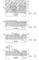
- FIG. 1(a) fuses 20 are fabricated in a polysilicon conductive layer that is surrounded by silicon dioxide 22. Bonding pads 24 are fabricated in a metal layer, which is covered by a layer of silicon dioxide 26 and a layer of silicon nitride 28, as in FIG. 1(b).
- a pix coating 30, e.g., a polymide resin, is laid over the silicon nitride patterned, and cured to provide access to the pads and fuses, as in FIGS. 1(c) and (d).
- the pix coating, the silicon nitride, and the silicon dioxide are etched away from the pads for direct access for electrical testing, as shown in FIG. 1(e) and 1(f).
- the pix coating, the silicon nitride, and a part of the silicon dioxide are etched away from above the fuses for laser trimming, as shown in FIG. 1(g).
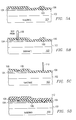
- test fuses 40 are fabricated in a polysilicon conductive layer surrounded by silicon dioxide 42 similar to the first method, as shown in FIG. 2(a). Thereafter a cap oxide 44, e.g., silicon dioxide, is deposited over the metallic layer 46 and silicon dioxide 42. The cap oxide is sintered and the surface of the device is patterned to nearly expose the fuses 40 of the device, as shown in FIG. 2(b). The cap oxide also is etched away from over the pads 46. The silicon dioxide is etched down nearly to the level of the fuses.
- electrical tests are performed through probes 48 contacting with the exposed pads, and a laser beam 50 is used for trimming fuses, as shown in FIG. 2(d).
- a silicon nitride layer 52 is deposited over the top of the device and into the fuse cavity, as shown in FIG. 2(e).
- a pix coating 54 is laid over the silicon nitride 52 and patterned to provide access to the pads, as shown in FIG 2(f).
- the pix material and the silicon nitride are etched to expose the pads for use in a system, as--shown in FIGS. 2(g) and 2(h).
- Bonding wires 56 are connected to the bonding pads 46, and a molding compound 58 is added to encapsulate the device.
- a disadvantage to this method is that a second costly masking sequence is added into the sequence of processing steps.
- An advantage in this process is that the silicon nitride protects the non-trimmed fuses from deleterious effects which can occur if those fuses are left unprotected from the ambient atmosphere.
- a method for fabricating a semiconductor device including the steps of: forming fuses in a first metallic layer; covering the first metallic layer with an insulator layer; forming conductive pads in a second metallic layer; depositing a layer of cap oxide over the pads and the insulator layer; etching back the layer of cap oxide until the top surfaces of the conductive pads and of the insulator layer over the fuses are exposed and sidewall oxides remain on the conducting pads; performing electrical tests; trimming at least a part of the fuses with a laser beam; depositing a silicon nitride layer; depositing a mask coating over the silicon nitride layer; patterning the mask coating for exposing the conductive pads; and etching the pix coating and the silicon nitride layer to expose the conductive pads.
- An advantage of this method is that it is relatively low cost because only one masking sequence is used in the sequence of steps. Risk of deleterious effects is low because the fuses are covered by the silicon nitride after the laser trimming operation.
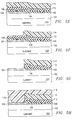
- FIGS. 3(a) through 3(i) there is shown a new sequence of steps in the process of fabricating an integrated circuit semiconductor device. This sequence of steps relates to the testing of circuits within the device, and to the switching good redundant circuits in replacement of defective regular circuits.
- FIG. 3(a) there is shown a fuse 60 fabricated in a metallic layer surrounded by a dielectric 62, such as silicon dioxide 62.
- the dielectric 62 is laid over a silicon substrate 63.
- a conductive metallic pad 64 formed for making interconnections between circuits built within the device (but not shown) and other external circuits.
- a layer of dielectric cap oxide 66 which may be silicon dioxide, is laid over the pad 64.
- a sinter operation is performed at this stage of device fabrication.
- the device is shown following an overall cap oxide etch back which removes the cap oxide 66 down to the top surface of the conductive pad 64 and to the top surface insulator 62.
- a sidewall insulator 67 is left on the conductive pad 64.
- the silicon dioxide cap oxide mixture of CHF 3 , CF 4 and Ar may be used in a ratio of approximately 20/20/1000.
- FIG. 3(c) shows an electrical probe from a testing apparatus making contact with the conductive pad 64 for making quality control tests. Some circuit defects may be uncovered as a result of the tests. Some of those defects can be removed from active operation of the device and can be replaced by other good redundant circuits by opening one or more fuses in the device.
- FIG. 3(d) shows a laser beam 70 which is used for blowing a fuse leaving a blow fuse cavity where the fuse 60 had been located. After all of the fuses are blown, as desired, an insulative layer 72, such as silicon nitride Si 3 N 4 is over the entire device and filling in the blown fuse cavities, as shown in FIG. 3(e).
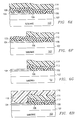
- an insulative layer 72 such as silicon nitride Si 3 N 4 is over the entire device and filling in the blown fuse cavities, as shown in FIG. 3(e).
- FIG. 3(f) there is shown a masking material 74 laid over the top of the device. This may be a photoresist that can be patterned and cured for exposing the conductive pads 64, as shown in FIG. 3(g).
- the patterned mask is used for etching back the insulative layer of silicon nitride to fully expose the conductive pads 64.
- a gas mixture of CF 4 , oxygen, and nitrogen in a ratio of 120/30/20 may be used for the etching of the silicon nitride.
- bonding wires such as the wire 76, are bonded to the conductive pad 64 for interconnecting with external circuits, which are not shown.
- a molding compound 78 is applied thereafter to protect the device from harmful effect of the atmosphere and other hazards.
- the etching is accomplished without the need for a mask.
- the etching is applied universally over the entire device. This saves an otherwise expense sequence of steps for forming and removing masking material.
- the bonding pads are exposed for testing while the top level of metallic wiring retains sidewall oxide to prevent electrical shorting and hillock growth.
- the silicon nitride film is applied to improve reliability by preventing deleterious effects caused by ambient atmospheric conditions. Additional area consuming moisture barrier structures are not used.
- a lower cost sequence of process steps are presented for making electrical tests, for trimming desired fuses, and for providing good hermetic sealing.
- FIGS. 4(a) through 4(h) there is presented another low cost sequence of steps for testing internal circuits of a semiconductor device and replacing defective ones of them with good redundant circuits.
- the device is shown including a fuse 80 surrounded by a dielectric 82 over a semiconductor substrate 83.
- a conductive pad 84 is laid on top of the dielectric 84.
- the fuse 80 and conductive pad 84 represent many of each.
- a test probe is connected to the conductive pad 84 for performing electrical tests, as shown in FIG. 4(b).
- defective circuits are replaced by good redundant circuits by laser beam 88 trimming of the fuses.
- a fuse cavity is opened where fuses are blown.
- a dielectric layer 90 of silicon nitride Si 3 N 4 is laid universally over the top of the device to cover the conductive pads 84 and to fill the fuse cavities.
- a masking material 92 such as a photoresist, is laid over the entire device, as shown in FIG. 4(e).
- the masking material 92 is patterned for exposing the conductive pad and is cured. Then the silicon nitride layer is etched back from the top of the conductive pads 84 to expose those pads.
- the previously mentioned mixture of CF 4 , oxygen, and nitrogen can be used as the etchant. Bonding wires, such as the wire 94, are connected to the conductive pads 84 and a molding compound 96 is applied.
- This sequence of processing steps has the further advantage of eliminating the steps of applying the cap oxide and etching back, as included in the sequence of FIG. 3.
- FIGS. 5(a) through 5(h) there is shown another variation of the new sequence of steps for testing for defective circuits and for replacing defective ones with good ones.
- the device is shown including a metallicfuse 100 fabricated in the same metal level as the conductive pad 104 on the top surface of an cap oxide insulator layer 102, which may be silicon dioxide. They are fabricated on top of a substrate 103. An insulative layer of silicon dioxide 106 covers the fuses 100, the conductive pads 104, and the silicon dioxide 102.
- a test probe 108 is mechanically pushed through the cap oxide 106 to contact the conductive pad 104 for testing internal circuits, not shown. Defective circuits are replaced by good redundant circuits by laser beam 110 trimming, as shown in FIG. 5(c). Cavities are left in the cap oxide 106 where the test probe was inserted and where any fuse was blown.
- a layer of silicon nitride 112 is laid over the entire device to cover the conductive pads 104 and the cap oxide 106 and to fill cavities in the cap oxide. Thereafter a masking material 114 is deposited overall, as shown in FIG. 5(e), is patterned, and is cured for exposing the conductive pads 104, as shown in FIG. 5(f).
- the silicon nitride layer 112 and the cap oxide are etched back to expose the surface of the conductive pads 104. Appropriate etchants are used. Finally bonding wires 116 are connected to the conductive pads 104 and a molding compound 118 is applied to protect the device.
- the cost of the testing and redundancy replacement steps is reduced because the conductive pads are exposed for testing without a sequence of masking steps, and additional moisture barrier structures are avoided.
- FIGS. 6(a) through 6(h) there is shown a further variation for testing and for replacing defective circuits.
- the sequence of steps is similar to the sequence of steps shown in FIGS. 5(a) through 5(h) so identical reference numerals are used to represent the same elements.
- the sequence of steps is identical except for the step shown in FIG. 6(b).
- a chemical etch is used to aid penetration through the cap oxide.
- the probe is first partially immersed in an etchant 120 and then is pressed through the cap oxide 106 to contact the conductive pad 104.
Abstract
Description
- This invention relates to a process for fabricating an integrated circuit device and more particularly to a method for making a laser repair in the device.
- During the process of fabricating integrated circuit devices, there are redundant circuits and other optional circuit arrangements which can be selected to assure desired operating functions. Such selections can be made by trimming certain fuses included in the device. Generally, a laser beam is used for trimming the fuses. An electrical test procedure is accomplished in conjunction with the laser trimming process.
- As shown in the sequence of FIGS. 1(a) through 1(h), there is shown a somewhat uneconomical prior art method for making laser repairs. In FIG. 1(a)
fuses 20 are fabricated in a polysilicon conductive layer that is surrounded bysilicon dioxide 22.Bonding pads 24 are fabricated in a metal layer, which is covered by a layer ofsilicon dioxide 26 and a layer ofsilicon nitride 28, as in FIG. 1(b). Apix coating 30, e.g., a polymide resin, is laid over the silicon nitride patterned, and cured to provide access to the pads and fuses, as in FIGS. 1(c) and (d). The pix coating, the silicon nitride, and the silicon dioxide are etched away from the pads for direct access for electrical testing, as shown in FIG. 1(e) and 1(f). The pix coating, the silicon nitride, and a part of the silicon dioxide are etched away from above the fuses for laser trimming, as shown in FIG. 1(g). An advantage of this process is that only a single photoresist mask step is used in the sequence of processing steps. Thereafter the electrical tests and the laser trimming are performed, but there aredevice moisture barriers 35 to prevent contamination caused by ambient atmospheric conditions. - These
moisture barriers 35 occupy a substantial area in addition to the circuit area and therefore raise the cost of making the device. The remaining partially exposed fuses may suffer corrosion or other deleterious effects from the exposure causing the device to subsequently malfunction. Moldingcompound 38 which is applied thereafter does not protect the device from harmful effects of the ambient atmosphere. - In another prior art method,
test fuses 40 are fabricated in a polysilicon conductive layer surrounded bysilicon dioxide 42 similar to the first method, as shown in FIG. 2(a). Thereafter acap oxide 44, e.g., silicon dioxide, is deposited over themetallic layer 46 andsilicon dioxide 42. The cap oxide is sintered and the surface of the device is patterned to nearly expose thefuses 40 of the device, as shown in FIG. 2(b). The cap oxide also is etched away from over thepads 46. The silicon dioxide is etched down nearly to the level of the fuses. In FIG. 2(c) electrical tests are performed throughprobes 48 contacting with the exposed pads, and alaser beam 50 is used for trimming fuses, as shown in FIG. 2(d). Once the testing and laser trimming are completed, asilicon nitride layer 52 is deposited over the top of the device and into the fuse cavity, as shown in FIG. 2(e). Apix coating 54 is laid over thesilicon nitride 52 and patterned to provide access to the pads, as shown in FIG 2(f). The pix material and the silicon nitride are etched to expose the pads for use in a system, as--shown in FIGS. 2(g) and 2(h).Bonding wires 56 are connected to thebonding pads 46, and amolding compound 58 is added to encapsulate the device. A disadvantage to this method is that a second costly masking sequence is added into the sequence of processing steps. An advantage in this process is that the silicon nitride protects the non-trimmed fuses from deleterious effects which can occur if those fuses are left unprotected from the ambient atmosphere. - These and other problems are solved by a method for fabricating a semiconductor device including the steps of: forming fuses in a first metallic layer; covering the first metallic layer with an insulator layer; forming conductive pads in a second metallic layer; depositing a layer of cap oxide over the pads and the insulator layer; etching back the layer of cap oxide until the top surfaces of the conductive pads and of the insulator layer over the fuses are exposed and sidewall oxides remain on the conducting pads; performing electrical tests; trimming at least a part of the fuses with a laser beam; depositing a silicon nitride layer; depositing a mask coating over the silicon nitride layer; patterning the mask coating for exposing the conductive pads; and etching the pix coating and the silicon nitride layer to expose the conductive pads.
- An advantage of this method is that it is relatively low cost because only one masking sequence is used in the sequence of steps. Risk of deleterious effects is low because the fuses are covered by the silicon nitride after the laser trimming operation.
- Several variations of the single masking sequence are disclosed.
- A better understanding of the invention may be derived by reference to the drawings which represent exemplary process sequences and wherein:
- FIGS. 1(a)-1(h) present a prior art laser repair process sequence;
- FIGS. 2(a)-2(i) present another prior art laser repair process sequence;
- FIGS. 3(a)-3(i) present an exemplary laser repair process sequence in accordance with the invention;
- FIGS. 4(a)-4(h) present another exemplary laser repair process sequence in accordance with the invention;
- FIGS. 5(a)-5(h) present a further exemplary laser repair process sequence in accordance with the invention;
- FIGS. 6(a)-6(h) present yet another exemplary laser repair process sequence in accordance with the invention; and FIG. 7 shows a cross section of an integrated circuit device with vias and contacts for making connection between conducting layers.
- Referring now to FIGS. 3(a) through 3(i), there is shown a new sequence of steps in the process of fabricating an integrated circuit semiconductor device. This sequence of steps relates to the testing of circuits within the device, and to the switching good redundant circuits in replacement of defective regular circuits.
- Referring now to FIG. 3(a), there is shown a
fuse 60 fabricated in a metallic layer surrounded by a dielectric 62, such assilicon dioxide 62. The dielectric 62 is laid over asilicon substrate 63. On the top surface of the dielectric 62, there is a conductivemetallic pad 64 formed for making interconnections between circuits built within the device (but not shown) and other external circuits. A layer ofdielectric cap oxide 66, which may be silicon dioxide, is laid over thepad 64. Although asingle fuse 60 and asingle pad 64 are shown, they are considered to be representative of a plurality of similar circuit elements which are not shown for purposes of clarifying the drawing. - A sinter operation is performed at this stage of device fabrication.
- In FIG. 3(b), the device is shown following an overall cap oxide etch back which removes the
cap oxide 66 down to the top surface of theconductive pad 64 and to thetop surface insulator 62. Asidewall insulator 67 is left on theconductive pad 64. For etching, the silicon dioxide cap oxide mixture of CHF3, CF4 and Ar may be used in a ratio of approximately 20/20/1000. - FIG. 3(c) shows an electrical probe from a testing apparatus making contact with the
conductive pad 64 for making quality control tests. Some circuit defects may be uncovered as a result of the tests. Some of those defects can be removed from active operation of the device and can be replaced by other good redundant circuits by opening one or more fuses in the device. - FIG. 3(d) shows a
laser beam 70 which is used for blowing a fuse leaving a blow fuse cavity where thefuse 60 had been located. After all of the fuses are blown, as desired, aninsulative layer 72, such as silicon nitride Si3N4 is over the entire device and filling in the blown fuse cavities, as shown in FIG. 3(e). - In FIG. 3(f), there is shown a
masking material 74 laid over the top of the device. This may be a photoresist that can be patterned and cured for exposing theconductive pads 64, as shown in FIG. 3(g). - Referring now to FIG. 3(h), the patterned mask is used for etching back the insulative layer of silicon nitride to fully expose the
conductive pads 64. A gas mixture of CF4, oxygen, and nitrogen in a ratio of 120/30/20 may be used for the etching of the silicon nitride. - Finally as shown in FIG. 3(i), bonding wires, such as the
wire 76, are bonded to theconductive pad 64 for interconnecting with external circuits, which are not shown. Amolding compound 78 is applied thereafter to protect the device from harmful effect of the atmosphere and other hazards. - Advantageously, after the sinter operation of the device in the form shown in FIG. 3(a), the etching is accomplished without the need for a mask. The etching is applied universally over the entire device. This saves an otherwise expense sequence of steps for forming and removing masking material. The bonding pads are exposed for testing while the top level of metallic wiring retains sidewall oxide to prevent electrical shorting and hillock growth. After the desired fused are trimmed, or blown, the silicon nitride film is applied to improve reliability by preventing deleterious effects caused by ambient atmospheric conditions. Additional area consuming moisture barrier structures are not used. Thus a lower cost sequence of process steps are presented for making electrical tests, for trimming desired fuses, and for providing good hermetic sealing.
- Referring now to FIGS. 4(a) through 4(h), there is presented another low cost sequence of steps for testing internal circuits of a semiconductor device and replacing defective ones of them with good redundant circuits.
- Referring now to FIG. 4(a), the device is shown including a
fuse 80 surrounded by a dielectric 82 over asemiconductor substrate 83. Aconductive pad 84 is laid on top of the dielectric 84. Thefuse 80 andconductive pad 84 represent many of each. At this stage of fabrication sintering is carried out. After the sintering operation, a test probe is connected to theconductive pad 84 for performing electrical tests, as shown in FIG. 4(b). - In FIG. 4(c), defective circuits (not shown) are replaced by good redundant circuits by
laser beam 88 trimming of the fuses. A fuse cavity is opened where fuses are blown. Adielectric layer 90 of silicon nitride Si3N4 is laid universally over the top of the device to cover theconductive pads 84 and to fill the fuse cavities. Then a maskingmaterial 92, such as a photoresist, is laid over the entire device, as shown in FIG. 4(e). - As shown in FIG 4(f), the masking
material 92 is patterned for exposing the conductive pad and is cured. Then the silicon nitride layer is etched back from the top of theconductive pads 84 to expose those pads. The previously mentioned mixture of CF4, oxygen, and nitrogen can be used as the etchant. Bonding wires, such as thewire 94, are connected to theconductive pads 84 and amolding compound 96 is applied. - This sequence of processing steps has the further advantage of eliminating the steps of applying the cap oxide and etching back, as included in the sequence of FIG. 3.
- Referring now to FIGS. 5(a) through 5(h), there is shown another variation of the new sequence of steps for testing for defective circuits and for replacing defective ones with good ones.
- In FIG. 5(a), the device is shown including a
metallicfuse 100 fabricated in the same metal level as theconductive pad 104 on the top surface of an capoxide insulator layer 102, which may be silicon dioxide. They are fabricated on top of asubstrate 103. An insulative layer ofsilicon dioxide 106 covers thefuses 100, theconductive pads 104, and thesilicon dioxide 102. - As shown in FIG. 5(b), a
test probe 108 is mechanically pushed through thecap oxide 106 to contact theconductive pad 104 for testing internal circuits, not shown. Defective circuits are replaced by good redundant circuits bylaser beam 110 trimming, as shown in FIG. 5(c). Cavities are left in thecap oxide 106 where the test probe was inserted and where any fuse was blown. - In FIG. 5(d), a layer of
silicon nitride 112 is laid over the entire device to cover theconductive pads 104 and thecap oxide 106 and to fill cavities in the cap oxide. Thereafter a maskingmaterial 114 is deposited overall, as shown in FIG. 5(e), is patterned, and is cured for exposing theconductive pads 104, as shown in FIG. 5(f). - In FIG. 5(g), the
silicon nitride layer 112 and the cap oxide are etched back to expose the surface of theconductive pads 104. Appropriate etchants are used. Finally bondingwires 116 are connected to theconductive pads 104 and amolding compound 118 is applied to protect the device. - Advantageously, the cost of the testing and redundancy replacement steps is reduced because the conductive pads are exposed for testing without a sequence of masking steps, and additional moisture barrier structures are avoided.
- Referring now to FIGS. 6(a) through 6(h), there is shown a further variation for testing and for replacing defective circuits. The sequence of steps is similar to the sequence of steps shown in FIGS. 5(a) through 5(h) so identical reference numerals are used to represent the same elements.
- The sequence of steps is identical except for the step shown in FIG. 6(b). Instead of mechanically breaking through the cap oxide with a
test probe 108, a chemical etch is used to aid penetration through the cap oxide. Thus the probe is first partially immersed in anetchant 120 and then is pressed through thecap oxide 106 to contact theconductive pad 104. - Thus a new less costly sequence of processing steps has been presented for electrically testing an integrated circuit device and for replacing defective circuits with good redundant circuits. Some variations of the sequence also have been presented. The disclosed processing sequences and others made obvious in view thereof are considered to be covered by the appended claims.
Claims (9)
- A method for fabricating a semiconductor device, the method including the steps of:forming fuses in a metallic layer, the fuses being surrounded by an insulator on a semiconductor substrate;forming bonding pads in a metallic layer formed on the insulator;sintering the device;performing an electrical test by way of the bonding pads;trimming at least a part of the fuses with a laser beam; anddepositing a layer of silicon nitride over the bonding pads and the insulator.
- The method for fabricating a semiconductor device, in accordance with claim 1 and including the further steps of:depositing a pix coating over the layer of silicon nitride;patterning the pix coating for exposing the pads;etching the pix coating and the layer of silicon nitride to expose the bonding pads; andattaching bonding wires to the exposed bonding pads.
- A method for fabricating a semiconductor device, as claimed in claim 1 or claim 2 the method including the step depositing a layer of cap oxide over the pads and the insulator.
- A method as claimed in claim 3 and including the step of etching back the entire layer of cap oxide except for sidewall oxides remaining on the bonding pads.
- A method as claimed in any preceding claim and wherein the fuses are formed in a first metallic layer and the bond pads are formed in a second metallic layer.
- A method for fabricating a semiconductor device as claimed in any preceding claim, the method including the steps of:forcing electrical probes through a cap oxide formed over the bonding pads to contact separate ones of said bonding pads; andperforming an electrical test by way of the bonding pads;
- A method for fabricating a semiconductor device, as claimed in claim 6 and wherein said forcing is etch assisted.
- The method for fabricating a semiconductor device, as claimed in any preceding claim and including the further steps of:depositing a pix coating over the layer of silicon nitride;patterning the pix coating for exposing the bonding pads;etching the pix coating and the layer of silicon nitride to expose the bonding pads; andattaching bonding wires to the exposed bonding pads.
- A semi-conductor device formed by the method of any preceding claim or having the structure of a device so formed.
Applications Claiming Priority (2)
| Application Number | Priority Date | Filing Date | Title |
|---|---|---|---|
| US08/413,291 US5641701A (en) | 1995-03-30 | 1995-03-30 | Method for fabricating a semiconductor device with laser programable fuses |
| US413291 | 1995-03-30 |
Publications (2)
| Publication Number | Publication Date |
|---|---|
| EP0735576A2 true EP0735576A2 (en) | 1996-10-02 |
| EP0735576A3 EP0735576A3 (en) | 1999-01-13 |
Family
ID=23636671
Family Applications (1)
| Application Number | Title | Priority Date | Filing Date |
|---|---|---|---|
| EP96302136A Withdrawn EP0735576A3 (en) | 1995-03-30 | 1996-03-27 | Integrated circuit fabrication |
Country Status (5)
| Country | Link |
|---|---|
| US (1) | US5641701A (en) |
| EP (1) | EP0735576A3 (en) |
| JP (1) | JPH08274180A (en) |
| KR (1) | KR100384964B1 (en) |
| TW (1) | TW319907B (en) |
Cited By (1)
| Publication number | Priority date | Publication date | Assignee | Title |
|---|---|---|---|---|
| DE10123686C1 (en) * | 2001-05-15 | 2003-03-20 | Infineon Technologies Ag | Method for producing an electronic component, in particular a memory chip, and electronic component produced thereby |
Families Citing this family (10)
| Publication number | Priority date | Publication date | Assignee | Title |
|---|---|---|---|---|
| JPH10163867A (en) * | 1996-11-29 | 1998-06-19 | Ricoh Co Ltd | Clock generator and its production |
| KR100241061B1 (en) * | 1997-07-26 | 2000-02-01 | 윤종용 | Semiconductor having fuse and method of manufacturing thereof |
| KR100502401B1 (en) * | 1997-09-03 | 2005-10-06 | 삼성전자주식회사 | Control tool for interferometer optic module |
| US6017824A (en) * | 1998-11-16 | 2000-01-25 | Taiwan Semiconductor Manufacturing Company | Passivation etching procedure, using a polysilicon stop layer, for repairing embedded DRAM cells |
| US6177297B1 (en) * | 1999-01-11 | 2001-01-23 | United Microelectronics Corp. | Method of forming metallic fuse demanding lower laser power for circuit repair |
| US6210995B1 (en) | 1999-09-09 | 2001-04-03 | International Business Machines Corporation | Method for manufacturing fusible links in a semiconductor device |
| US6667195B2 (en) * | 2001-08-06 | 2003-12-23 | United Microelectronics Corp. | Laser repair operation |
| KR100449029B1 (en) * | 2002-04-04 | 2004-09-16 | 삼성전자주식회사 | Semiconductor device with fuse box in pad region and method for fabricating the same |
| TWI243455B (en) | 2002-11-27 | 2005-11-11 | Siliconware Precision Industries Co Ltd | Ball grid array semiconductor package |
| CN113013090B (en) * | 2021-02-07 | 2022-06-24 | 长鑫存储技术有限公司 | Fusing filling method of semiconductor structure and semiconductor structure |
Citations (6)
| Publication number | Priority date | Publication date | Assignee | Title |
|---|---|---|---|---|
| EP0128675A1 (en) * | 1983-05-16 | 1984-12-19 | Fujitsu Limited | A method of fabricating an integrated circuit having multi-layer wiring with a fuse and a fuse opening |
| US4602420A (en) * | 1984-02-23 | 1986-07-29 | Kabushiki Kaisha Toshiba | Method of manufacturing a semiconductor device |
| US5025300A (en) * | 1989-06-30 | 1991-06-18 | At&T Bell Laboratories | Integrated circuits having improved fusible links |
| US5241212A (en) * | 1990-05-01 | 1993-08-31 | Mitsubishi Denki Kabushiki Kaisha | Semiconductor device having a redundant circuit portion and a manufacturing method of the same |
| US5252844A (en) * | 1988-11-17 | 1993-10-12 | Mitsubishi Denki Kabushiki Kaisha | Semiconductor device having a redundant circuit and method of manufacturing thereof |
| US5326709A (en) * | 1991-12-19 | 1994-07-05 | Samsung Electronics Co., Ltd. | Wafer testing process of a semiconductor device comprising a redundancy circuit |
Family Cites Families (1)
| Publication number | Priority date | Publication date | Assignee | Title |
|---|---|---|---|---|
| JPH0737988A (en) * | 1993-07-20 | 1995-02-07 | Hitachi Ltd | Manufacture of semiconductor integrated circuit device |
-
1995
- 1995-03-30 US US08/413,291 patent/US5641701A/en not_active Expired - Lifetime
-
1996
- 1996-03-27 EP EP96302136A patent/EP0735576A3/en not_active Withdrawn
- 1996-03-29 JP JP8077123A patent/JPH08274180A/en active Pending
- 1996-03-29 KR KR1019960009130A patent/KR100384964B1/en active IP Right Grant
- 1996-04-25 TW TW085104920A patent/TW319907B/zh not_active IP Right Cessation
Patent Citations (6)
| Publication number | Priority date | Publication date | Assignee | Title |
|---|---|---|---|---|
| EP0128675A1 (en) * | 1983-05-16 | 1984-12-19 | Fujitsu Limited | A method of fabricating an integrated circuit having multi-layer wiring with a fuse and a fuse opening |
| US4602420A (en) * | 1984-02-23 | 1986-07-29 | Kabushiki Kaisha Toshiba | Method of manufacturing a semiconductor device |
| US5252844A (en) * | 1988-11-17 | 1993-10-12 | Mitsubishi Denki Kabushiki Kaisha | Semiconductor device having a redundant circuit and method of manufacturing thereof |
| US5025300A (en) * | 1989-06-30 | 1991-06-18 | At&T Bell Laboratories | Integrated circuits having improved fusible links |
| US5241212A (en) * | 1990-05-01 | 1993-08-31 | Mitsubishi Denki Kabushiki Kaisha | Semiconductor device having a redundant circuit portion and a manufacturing method of the same |
| US5326709A (en) * | 1991-12-19 | 1994-07-05 | Samsung Electronics Co., Ltd. | Wafer testing process of a semiconductor device comprising a redundancy circuit |
Cited By (2)
| Publication number | Priority date | Publication date | Assignee | Title |
|---|---|---|---|---|
| DE10123686C1 (en) * | 2001-05-15 | 2003-03-20 | Infineon Technologies Ag | Method for producing an electronic component, in particular a memory chip, and electronic component produced thereby |
| US7338843B2 (en) | 2001-05-15 | 2008-03-04 | Infineon Technologies Ag | Method for producing an electronic component, especially a memory chip |
Also Published As
| Publication number | Publication date |
|---|---|
| US5641701A (en) | 1997-06-24 |
| JPH08274180A (en) | 1996-10-18 |
| EP0735576A3 (en) | 1999-01-13 |
| TW319907B (en) | 1997-11-11 |
| KR100384964B1 (en) | 2003-08-21 |
Similar Documents
| Publication | Publication Date | Title |
|---|---|---|
| US8901733B2 (en) | Reliable metal bumps on top of I/O pads after removal of test probe marks | |
| US4628590A (en) | Method of manufacture of a semiconductor device | |
| EP0128675B1 (en) | A method of fabricating an integrated circuit having multi-layer wiring with a fuse and a fuse opening | |
| US5023205A (en) | Method of fabricating hybrid circuit structures | |
| EP0523856A2 (en) | Method of via formation for multilevel interconnect integrated circuits | |
| JP3881393B2 (en) | Manufacturing method of semiconductor device | |
| KR100447968B1 (en) | method of fabricating wafer level package | |
| US5641701A (en) | Method for fabricating a semiconductor device with laser programable fuses | |
| JPH1084042A (en) | Semiconductor device and its manufacturing method as well as forming method of polysilicon fuse at the small pitch in semiconductor | |
| US5474651A (en) | Method for filling via holes in a semiconductor layer structure | |
| US20020182837A1 (en) | Antifuse for use with low kappa dielectric foam insulators | |
| US6022762A (en) | Process for forming a morphological edge structure to seal integrated electronic devices | |
| US4882293A (en) | Method of making an electrically programmable integrated circuit containing meltable contact bridges | |
| US5789796A (en) | Programmable anti-fuse device and method for manufacturing the same | |
| US6248657B1 (en) | Semiconductor device and method for manufacturing the same | |
| US7785935B2 (en) | Manufacturing method for forming an integrated circuit device and corresponding integrated circuit device | |
| EP0583119A1 (en) | Programmable contact structure and its forming method | |
| US5610100A (en) | Method for concurrently forming holes for interconnection between different conductive layers and a substrate element or circuit element close to the substrate surface | |
| KR940007290B1 (en) | Manufacturing method of wirebonding pad | |
| US7763951B2 (en) | Fuse structure for maintaining passivation integrity | |
| KR0177405B1 (en) | Semiconductor device and manufacture thereof | |
| KR20020001019A (en) | Method of fabricating semiconductor device with fuse | |
| KR0151224B1 (en) | Isolation method of a semiconductor device | |
| KR100216730B1 (en) | Semiconductor metal film etching step | |
| KR19990018323A (en) | Method of manufacturing multilayer antifuse of semiconductor device |
Legal Events
| Date | Code | Title | Description |
|---|---|---|---|
| PUAI | Public reference made under article 153(3) epc to a published international application that has entered the european phase |
Free format text: ORIGINAL CODE: 0009012 |
|
| AK | Designated contracting states |
Kind code of ref document: A2 Designated state(s): DE FR GB IT NL |
|
| PUAL | Search report despatched |
Free format text: ORIGINAL CODE: 0009013 |
|
| RHK1 | Main classification (correction) |
Ipc: H01L 21/268 |
|
| AK | Designated contracting states |
Kind code of ref document: A3 Designated state(s): DE FR GB IT NL |
|
| 17P | Request for examination filed |
Effective date: 19990709 |
|
| 17Q | First examination report despatched |
Effective date: 20040205 |
|
| STAA | Information on the status of an ep patent application or granted ep patent |
Free format text: STATUS: THE APPLICATION IS DEEMED TO BE WITHDRAWN |
|
| 18D | Application deemed to be withdrawn |
Effective date: 20040817 |