EP0686979B1 - Failure tolerant memory device, in particular of the flash EEPROM type - Google Patents
Failure tolerant memory device, in particular of the flash EEPROM type Download PDFInfo
- Publication number
- EP0686979B1 EP0686979B1 EP94830283A EP94830283A EP0686979B1 EP 0686979 B1 EP0686979 B1 EP 0686979B1 EP 94830283 A EP94830283 A EP 94830283A EP 94830283 A EP94830283 A EP 94830283A EP 0686979 B1 EP0686979 B1 EP 0686979B1
- Authority
- EP
- European Patent Office
- Prior art keywords
- cells
- cell
- deletion
- accordance
- gain
- Prior art date
- Legal status (The legal status is an assumption and is not a legal conclusion. Google has not performed a legal analysis and makes no representation as to the accuracy of the status listed.)
- Expired - Lifetime
Links
Images

Classifications
-
- G—PHYSICS
- G11—INFORMATION STORAGE
- G11C—STATIC STORES
- G11C29/00—Checking stores for correct operation ; Subsequent repair; Testing stores during standby or offline operation
- G11C29/70—Masking faults in memories by using spares or by reconfiguring
- G11C29/78—Masking faults in memories by using spares or by reconfiguring using programmable devices
- G11C29/80—Masking faults in memories by using spares or by reconfiguring using programmable devices with improved layout
- G11C29/816—Masking faults in memories by using spares or by reconfiguring using programmable devices with improved layout for an application-specific layout
- G11C29/82—Masking faults in memories by using spares or by reconfiguring using programmable devices with improved layout for an application-specific layout for EEPROMs
-
- G—PHYSICS
- G11—INFORMATION STORAGE
- G11C—STATIC STORES
- G11C16/00—Erasable programmable read-only memories
- G11C16/02—Erasable programmable read-only memories electrically programmable
- G11C16/06—Auxiliary circuits, e.g. for writing into memory
- G11C16/34—Determination of programming status, e.g. threshold voltage, overprogramming or underprogramming, retention
-
- G—PHYSICS
- G11—INFORMATION STORAGE
- G11C—STATIC STORES
- G11C29/00—Checking stores for correct operation ; Subsequent repair; Testing stores during standby or offline operation
- G11C29/04—Detection or location of defective memory elements, e.g. cell constructio details, timing of test signals
- G11C29/50—Marginal testing, e.g. race, voltage or current testing
-
- G—PHYSICS
- G06—COMPUTING; CALCULATING OR COUNTING
- G06F—ELECTRIC DIGITAL DATA PROCESSING
- G06F2201/00—Indexing scheme relating to error detection, to error correction, and to monitoring
- G06F2201/81—Threshold
-
- G—PHYSICS
- G11—INFORMATION STORAGE
- G11C—STATIC STORES
- G11C16/00—Erasable programmable read-only memories
- G11C16/02—Erasable programmable read-only memories electrically programmable
- G11C16/04—Erasable programmable read-only memories electrically programmable using variable threshold transistors, e.g. FAMOS
-
- G—PHYSICS
- G11—INFORMATION STORAGE
- G11C—STATIC STORES
- G11C29/00—Checking stores for correct operation ; Subsequent repair; Testing stores during standby or offline operation
- G11C29/04—Detection or location of defective memory elements, e.g. cell constructio details, timing of test signals
- G11C29/50—Marginal testing, e.g. race, voltage or current testing
- G11C2029/5006—Current
Description
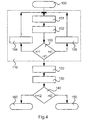
- 100
- method start
- 110
- cell conditioning - phase a. of the method
- 101
- apply V1
- 102
- detect I(V1)
- 103
- test on I(V1) in relation to I1
- 104
- deletion phase
- 105
- programming phase
- 120
- apply V2 - phase b. of the method
- 130
- detect I(V2) - phase c. of the method
- 140
- test on I(V2) in relation to I2 - phase d. of the method
- 150
- high-gain association - end of method phase e.
- 160
- low-gain association - end of method phase e.
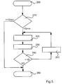
- 200
- method start
- 210
- gain test of cell G compared with Gmin
- 220
- apply V3
- 230
- detect I(V3)
- 240
- test on I(V3) compared with I3
- 250
- deletion phase
- 260
- method end
Claims (11)
- Method of discriminating -a memory cell of the single-transistor insulated gate memorisation type based on gain characterised in that it comprises the following phases:a) carry the insulated gate of the cell in a charge state such that by applying a first reading voltage (V1) to the gate terminal of the cell by means of successive programming and/or deletion and verification phases there is detected a first reading current (I(V1)) through the cell channel about equal to a first value (I1),b) apply a second reading voltage (V2) to the gate terminal of the cell, said second reading voltage (V2) differing from said first reading voltage (V1),c) detect a second current (I(V2)) through the cell channel corresponding to the second reading voltage (V2),d) compare the value of the second reading current (I(V2)) with a second value (I2), ande) associate the cell alternatively with a first or a second class of cells based on the outcome of said comparison.
- Method in accordance with claim 1 in which said second reading voltage (V2) is higher than said first reading voltage (V1) and in which said second value (I2) is higher than said first value (I1) and in which said cell is associated with a first class of high-gain cells if from said comparison it proves that said second reading current (I(V2)) is higher than said second value (I2) and otherwise is associated with a second class of low-gain cells.
- Method according to claim 1, further comprises at least one series of successive deletion and individual verification phases of the cell deletion state, said individual verification phases affecting only the high-gain cells.
- Method in accordance with claim 3 in which said discrimination phase takes place in accordance with the method set forth in claims 1 or 2 before said series of successive deletion and verification phases.
- Method in accordance with claim 3 or 4 in which the cells not high-gain are considered faulty.
- Method in accordance with claim 5 in which at least said faulty cells are replaced by redundant cells.
- Method in accordance with claim 6 in which said redundant cells experience on average the same life as the non-redundant cells before said replacement.
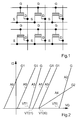
- Memory device of the type comprising:characterised in that said decoding means (RDEC,CDEC) comprise at least one non-volatile memory (NVM) for mapping said addresses and that said control logic (CL) comprises means (TST) designed to identify cell faults in said rows and/or columns by comparing the cells' gains and writing means (WM) designed to write on said non-volatile memory (NVM) addresses corresponding to said at least one redundant row and/or column (RID) to rectify said faults.a.) matrix (MAT) of memory cells having a plurality of rows and columns of which at least one row and/or column (RID) is redundant,b) decoding means (RDEC,CDEC) for row and/or column addresses,c.) control logic (CL) for writing, reading and deletion of the cells and control of the device components,d) means for applying a voltage to the gate terminal of cell, ande) means for detecting a current through the cell channel,
- Device in accordance with claim 8 in which said control logic (CL) comprises additionally discrimination means (TST) for said cells on the basis of gain and designed to pilot said writing means (WM).
- Device in accordance with claim 9 in which said control logic (CL) operates for deletion in accordance with the method set forth in one of the claims from 3 to 7.
- Integrated circuit comprising a memory device for storing data and/or programs characterised in that said memory device is the type set forth in claims 8 to 10.
Priority Applications (4)
| Application Number | Priority Date | Filing Date | Title |
|---|---|---|---|
| DE69426818T DE69426818T2 (en) | 1994-06-10 | 1994-06-10 | Fault-tolerant storage device, in particular of the "flash EEPROM" type |
| EP94830283A EP0686979B1 (en) | 1994-06-10 | 1994-06-10 | Failure tolerant memory device, in particular of the flash EEPROM type |
| US08/454,650 US5682349A (en) | 1994-06-10 | 1995-05-31 | Failure tolerant memory device, in particular of the flash EEPROM type |
| JP14503495A JP3725581B2 (en) | 1994-06-10 | 1995-06-12 | CELL DISCRIMINATION METHOD AND ERASE METHOD, MEMORY DEVICE USED FOR THEM, AND INTEGRATED CIRCUIT USING THE MEMORY DEVICE |
Applications Claiming Priority (1)
| Application Number | Priority Date | Filing Date | Title |
|---|---|---|---|
| EP94830283A EP0686979B1 (en) | 1994-06-10 | 1994-06-10 | Failure tolerant memory device, in particular of the flash EEPROM type |
Publications (2)
| Publication Number | Publication Date |
|---|---|
| EP0686979A1 EP0686979A1 (en) | 1995-12-13 |
| EP0686979B1 true EP0686979B1 (en) | 2001-03-07 |
Family
ID=8218466
Family Applications (1)
| Application Number | Title | Priority Date | Filing Date |
|---|---|---|---|
| EP94830283A Expired - Lifetime EP0686979B1 (en) | 1994-06-10 | 1994-06-10 | Failure tolerant memory device, in particular of the flash EEPROM type |
Country Status (4)
| Country | Link |
|---|---|
| US (1) | US5682349A (en) |
| EP (1) | EP0686979B1 (en) |
| JP (1) | JP3725581B2 (en) |
| DE (1) | DE69426818T2 (en) |
Families Citing this family (12)
| Publication number | Priority date | Publication date | Assignee | Title |
|---|---|---|---|---|
| GB9614551D0 (en) | 1996-07-11 | 1996-09-04 | Memory Corp Plc | Memory system |
| US6532556B1 (en) | 2000-01-27 | 2003-03-11 | Multi Level Memory Technology | Data management for multi-bit-per-cell memories |
| US6314023B1 (en) * | 2000-06-15 | 2001-11-06 | Motorola, Inc. | Non-volatile programming elements for redundancy and identification in an integrated circuit |
| US6466476B1 (en) | 2001-01-18 | 2002-10-15 | Multi Level Memory Technology | Data coding for multi-bit-per-cell memories having variable numbers of bits per memory cell |
| DE60212332T2 (en) * | 2002-04-26 | 2007-06-06 | Stmicroelectronics S.R.L., Agrate Brianza | Self-repair method for non-volatile memory with error-avoidance architecture and non-volatile memory |
| DE60230592D1 (en) | 2002-05-21 | 2009-02-12 | St Microelectronics Srl | Self-repair method for nonvolatile memory device with erase / program error detection, and nonvolatile memory device therefor |
| US6839275B2 (en) * | 2003-06-04 | 2005-01-04 | Hewlett-Packard Development Company, L.P. | Memory system having control circuit configured to receive data, provide encoded received data to match a fault pattern in the array of memory cells |
| US7046555B2 (en) | 2003-09-17 | 2006-05-16 | Sandisk Corporation | Methods for identifying non-volatile memory elements with poor subthreshold slope or weak transconductance |
| US7177189B2 (en) | 2004-03-01 | 2007-02-13 | Intel Corporation | Memory defect detection and self-repair technique |
| JP2006294144A (en) * | 2005-04-12 | 2006-10-26 | Toshiba Corp | Nonvolatile semiconductor memory device |
| EP1947539A4 (en) * | 2005-09-27 | 2011-05-18 | Advantest Corp | Control method, and control system |
| US7545679B1 (en) * | 2007-12-28 | 2009-06-09 | Freescale Semiconductor, Inc. | Electrical erasable programmable memory transconductance testing |
Family Cites Families (11)
| Publication number | Priority date | Publication date | Assignee | Title |
|---|---|---|---|---|
| EP0198935A1 (en) * | 1985-04-23 | 1986-10-29 | Deutsche ITT Industries GmbH | Electrically erasable programmable redundant semiconductor memory |
| JPS62114200A (en) * | 1985-11-13 | 1987-05-25 | Mitsubishi Electric Corp | Semiconductor memory device |
| DE69013237T2 (en) * | 1989-06-19 | 1995-02-23 | Texas Instruments Inc | Circuit and procedure for preparing deleted EEPROMS before programming. |
| US5233559A (en) * | 1991-02-11 | 1993-08-03 | Intel Corporation | Row redundancy for flash memories |
| KR960002006B1 (en) * | 1991-03-12 | 1996-02-09 | 가부시끼가이샤 도시바 | Eeprom with write/verify controller using two reference levels |
| JP3080743B2 (en) * | 1991-12-27 | 2000-08-28 | 日本電気株式会社 | Nonvolatile semiconductor memory device |
| KR960002777B1 (en) * | 1992-07-13 | 1996-02-26 | 삼성전자주식회사 | Row redundancy device for a semiconductor device |
| FR2694404B1 (en) * | 1992-07-31 | 1994-09-09 | Sgs Thomson Microelectronics | Method for measuring the threshold voltages of the cells of an integrated memory. |
| US5428621A (en) * | 1992-09-21 | 1995-06-27 | Sundisk Corporation | Latent defect handling in EEPROM devices |
| US5452251A (en) * | 1992-12-03 | 1995-09-19 | Fujitsu Limited | Semiconductor memory device for selecting and deselecting blocks of word lines |
| JP3212421B2 (en) * | 1993-09-20 | 2001-09-25 | 富士通株式会社 | Nonvolatile semiconductor memory device |
-
1994
- 1994-06-10 DE DE69426818T patent/DE69426818T2/en not_active Expired - Fee Related
- 1994-06-10 EP EP94830283A patent/EP0686979B1/en not_active Expired - Lifetime
-
1995
- 1995-05-31 US US08/454,650 patent/US5682349A/en not_active Expired - Lifetime
- 1995-06-12 JP JP14503495A patent/JP3725581B2/en not_active Expired - Lifetime
Also Published As
| Publication number | Publication date |
|---|---|
| EP0686979A1 (en) | 1995-12-13 |
| DE69426818D1 (en) | 2001-04-12 |
| JPH0883500A (en) | 1996-03-26 |
| DE69426818T2 (en) | 2001-10-18 |
| JP3725581B2 (en) | 2005-12-14 |
| US5682349A (en) | 1997-10-28 |
Similar Documents
| Publication | Publication Date | Title |
|---|---|---|
| US7437631B2 (en) | Soft errors handling in EEPROM devices | |
| US5532962A (en) | Soft errors handling in EEPROM devices | |
| EP0314180B1 (en) | Nonvolatile semiconductor memory having a stress test circuit | |
| US5659550A (en) | Latent defect handling in EEPROM devices | |
| US4733394A (en) | Electrically programmable semiconductor memory showing redundance | |
| US6646930B2 (en) | Non-volatile semiconductor memory | |
| KR0168896B1 (en) | Semiconductor memory of xn type having error correcting circuit by parity | |
| US5590075A (en) | Method for testing an electrically erasable and programmable memory device | |
| JP3450625B2 (en) | Nonvolatile semiconductor memory device and operation method thereof | |
| EP0686979B1 (en) | Failure tolerant memory device, in particular of the flash EEPROM type | |
| DE10026993B4 (en) | Flash memory device with a new redundancy drive circuit | |
| US20070047299A1 (en) | Method for accessing a multilevel nonvolatile memory device of the flash nand type | |
| JPH06267300A (en) | Nonvolatile semiconductor memory device, semiconductor device and testing method therefor | |
| US20070025167A1 (en) | Method for testing a memory device, test unit for testing a memory device and memory device | |
| DE102007016460A1 (en) | Non-volatile memory device, non-volatile memory system and reading method for a nonvolatile memory device | |
| KR900006160B1 (en) | Semicondcutor memory device | |
| JPH07296592A (en) | Nonvolatile semiconductor storage | |
| US6819589B1 (en) | Flash memory with pre-detection for data loss | |
| US20080285368A1 (en) | Method for nrom array word line retry erasing and threshold voltage recovering | |
| US6850437B2 (en) | Nonvolatile semiconductor memory device and method of retrieving faulty in the same | |
| JP2710237B2 (en) | Semiconductor memory device and method of replacing redundant memory cell portion thereof | |
| JP2001023397A (en) | Test method for semiconductor memory and semiconductor memory | |
| US5594693A (en) | Matrix device with redundancy fuses for integrated memory | |
| JP3384409B2 (en) | Rewritable nonvolatile semiconductor memory device and control method thereof | |
| US5561635A (en) | PROM IC enabling a stricter memory cell margin test |
Legal Events
| Date | Code | Title | Description |
|---|---|---|---|
| PUAI | Public reference made under article 153(3) epc to a published international application that has entered the european phase |
Free format text: ORIGINAL CODE: 0009012 |
|
| AK | Designated contracting states |
Kind code of ref document: A1 Designated state(s): DE FR GB IT |
|
| 17P | Request for examination filed |
Effective date: 19960601 |
|
| 17Q | First examination report despatched |
Effective date: 19980529 |
|
| RAP3 | Party data changed (applicant data changed or rights of an application transferred) |
Owner name: STMICROELECTRONICS S.R.L. |
|
| GRAG | Despatch of communication of intention to grant |
Free format text: ORIGINAL CODE: EPIDOS AGRA |
|
| GRAG | Despatch of communication of intention to grant |
Free format text: ORIGINAL CODE: EPIDOS AGRA |
|
| GRAH | Despatch of communication of intention to grant a patent |
Free format text: ORIGINAL CODE: EPIDOS IGRA |
|
| GRAH | Despatch of communication of intention to grant a patent |
Free format text: ORIGINAL CODE: EPIDOS IGRA |
|
| GRAA | (expected) grant |
Free format text: ORIGINAL CODE: 0009210 |
|
| STAA | Information on the status of an ep patent application or granted ep patent |
Free format text: STATUS: THE PATENT HAS BEEN GRANTED |
|
| AK | Designated contracting states |
Kind code of ref document: B1 Designated state(s): DE FR GB IT |
|
| REF | Corresponds to: |
Ref document number: 69426818 Country of ref document: DE Date of ref document: 20010412 |
|
| ET | Fr: translation filed | ||
| ITF | It: translation for a ep patent filed |
Owner name: BOTTI & FERRARI S.R.L. |
|
| REG | Reference to a national code |
Ref country code: GB Ref legal event code: IF02 |
|
| PLBE | No opposition filed within time limit |
Free format text: ORIGINAL CODE: 0009261 |
|
| 26N | No opposition filed | ||
| PGFP | Annual fee paid to national office [announced via postgrant information from national office to epo] |
Ref country code: DE Payment date: 20030610 Year of fee payment: 10 |
|
| PGFP | Annual fee paid to national office [announced via postgrant information from national office to epo] |
Ref country code: GB Payment date: 20040602 Year of fee payment: 11 |
|
| PGFP | Annual fee paid to national office [announced via postgrant information from national office to epo] |
Ref country code: FR Payment date: 20040628 Year of fee payment: 11 |
|
| PG25 | Lapsed in a contracting state [announced via postgrant information from national office to epo] |
Ref country code: DE Free format text: LAPSE BECAUSE OF NON-PAYMENT OF DUE FEES Effective date: 20050101 |
|
| PG25 | Lapsed in a contracting state [announced via postgrant information from national office to epo] |
Ref country code: IT Free format text: LAPSE BECAUSE OF NON-PAYMENT OF DUE FEES;WARNING: LAPSES OF ITALIAN PATENTS WITH EFFECTIVE DATE BEFORE 2007 MAY HAVE OCCURRED AT ANY TIME BEFORE 2007. THE CORRECT EFFECTIVE DATE MAY BE DIFFERENT FROM THE ONE RECORDED. Effective date: 20050610 Ref country code: GB Free format text: LAPSE BECAUSE OF NON-PAYMENT OF DUE FEES Effective date: 20050610 |
|
| PG25 | Lapsed in a contracting state [announced via postgrant information from national office to epo] |
Ref country code: FR Free format text: LAPSE BECAUSE OF NON-PAYMENT OF DUE FEES Effective date: 20060228 |
|
| GBPC | Gb: european patent ceased through non-payment of renewal fee |
Effective date: 20050610 |
|
| REG | Reference to a national code |
Ref country code: FR Ref legal event code: ST Effective date: 20060228 |