EP0686979A1 - Failure tolerant memory device, in particular of the flash EEPROM type - Google Patents
Failure tolerant memory device, in particular of the flash EEPROM type Download PDFInfo
- Publication number
- EP0686979A1 EP0686979A1 EP94830283A EP94830283A EP0686979A1 EP 0686979 A1 EP0686979 A1 EP 0686979A1 EP 94830283 A EP94830283 A EP 94830283A EP 94830283 A EP94830283 A EP 94830283A EP 0686979 A1 EP0686979 A1 EP 0686979A1
- Authority
- EP
- European Patent Office
- Prior art keywords
- cells
- cell
- gain
- accordance
- deletion
- Prior art date
- Legal status (The legal status is an assumption and is not a legal conclusion. Google has not performed a legal analysis and makes no representation as to the accuracy of the status listed.)
- Granted
Links
Images


Classifications
-
- G—PHYSICS
- G11—INFORMATION STORAGE
- G11C—STATIC STORES
- G11C29/00—Checking stores for correct operation ; Subsequent repair; Testing stores during standby or offline operation
- G11C29/70—Masking faults in memories by using spares or by reconfiguring
- G11C29/78—Masking faults in memories by using spares or by reconfiguring using programmable devices
- G11C29/80—Masking faults in memories by using spares or by reconfiguring using programmable devices with improved layout
- G11C29/816—Masking faults in memories by using spares or by reconfiguring using programmable devices with improved layout for an application-specific layout
- G11C29/82—Masking faults in memories by using spares or by reconfiguring using programmable devices with improved layout for an application-specific layout for EEPROMs
-
- G—PHYSICS
- G11—INFORMATION STORAGE
- G11C—STATIC STORES
- G11C16/00—Erasable programmable read-only memories
- G11C16/02—Erasable programmable read-only memories electrically programmable
- G11C16/06—Auxiliary circuits, e.g. for writing into memory
- G11C16/34—Determination of programming status, e.g. threshold voltage, overprogramming or underprogramming, retention
-
- G—PHYSICS
- G11—INFORMATION STORAGE
- G11C—STATIC STORES
- G11C29/00—Checking stores for correct operation ; Subsequent repair; Testing stores during standby or offline operation
- G11C29/04—Detection or location of defective memory elements, e.g. cell constructio details, timing of test signals
- G11C29/50—Marginal testing, e.g. race, voltage or current testing
-
- G—PHYSICS
- G06—COMPUTING; CALCULATING OR COUNTING
- G06F—ELECTRIC DIGITAL DATA PROCESSING
- G06F2201/00—Indexing scheme relating to error detection, to error correction, and to monitoring
- G06F2201/81—Threshold
-
- G—PHYSICS
- G11—INFORMATION STORAGE
- G11C—STATIC STORES
- G11C16/00—Erasable programmable read-only memories
- G11C16/02—Erasable programmable read-only memories electrically programmable
- G11C16/04—Erasable programmable read-only memories electrically programmable using variable threshold transistors, e.g. FAMOS
-
- G—PHYSICS
- G11—INFORMATION STORAGE
- G11C—STATIC STORES
- G11C29/00—Checking stores for correct operation ; Subsequent repair; Testing stores during standby or offline operation
- G11C29/04—Detection or location of defective memory elements, e.g. cell constructio details, timing of test signals
- G11C29/50—Marginal testing, e.g. race, voltage or current testing
- G11C2029/5006—Current
Landscapes
- For Increasing The Reliability Of Semiconductor Memories (AREA)
- Read Only Memory (AREA)
Abstract
Description
- The present invention relates to a memory device and in particular a flash EPROM in accordance with the preamble of claim 8 and a method for discriminating a gain-based insulated-gate single memorisation-transistor memory cell and to a method of deleting a memory cell of the same type. The memory device in accordance with the present invention can find advantageous application also in integrated circuits such as microprocessors and microcontrollers.
- In the area of non-volatile semiconductor memories, presently comprising the UV_EPROM, E_EPROM and flash EPROM, the memory device consists of a matrix of equal cells which comprise for the memorisation of the data a single MOS transistor having at least one insulated gate. The value 0 or 1 of the data memorised depends on the amount of charges present on the insulated gate which in turn determines the threshold voltage of the MOS transistor.
- As known, with the matrix must be connected row and/or column address decoding means and a control logic for reading, writing and deletion of the matrix cells.
- There are often provided in the matrix one or more redundant rows and/or one or more redundant columns. These are used during manufacturing testing to obviate manufacturing defects by replacing the rows or columns containing faults with redundant rows or columns.
- FIG. 1 shows a flash EPROM cell matrix with 2 rows and 3 columns.
- Various well known mechanisms are used for the programming and deletion operation which can take place either globally, i.e. they affect the entire matrix, or selectively. The reading operation consists of applying to the selected cell a polarization voltage (for writing) and detecting the corresponding current (for writing) and in comparing it with appropriate reference currents.
- In particular in flash EPROM memories, reading and programming are selective while deletion is done electrically and globally.
- Almost always, the programming and deletion operations take place by means of a series of identical successive phases. For programming, injection of 'hot electrons' and, for deletion, extraction of charges by the Fowler-Nordheim effect. After each individual programming or deletion phase there is a phase of verification of the charge present on the insulated gate of each cell. In this manner the charge status and consequently the threshold voltage of the individual cells can be controlled with great precision.
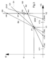
- FIG. 2 shows in a simplified manner the gate voltage versus channel current characteristics of cells having different charge status. In particular, A0 indicates the characteristic of a cell at instant t0 having a threshold voltage VT(t0) and gain G1 while A1 indicates the characteristic of the same cell at instant t1, following t0, after a deletion phase and thus having the same gain G1 but threshold voltage VT(t1) lower than VT(t0).
- The verification phase consists of a particular reading operation performed with particular reference currents more restrictive than those used for the normal reading operation.
- In flash EPROM devices it is extremely important that all the cells 'experience the same history', i.e. they must be programmed and deleted the same number of times. For this reason, before the actual deletion there is a programming operation of all the cells denominated 'preconditioning'.
- After the 'preconditioning' operation, all the cells have a threshold voltage higher than a pre-set value VT0. The characteristic indicated by A2 in FIG. 2 having a reference gain G represents the limit of the programming condition while after the subsequent deletion operation all the cells have a threshold voltage lower than a pre-set value VT1. The characteristic indicated by A3 in FIG. 2 having the same reference gain G represents the limit of the deletion condition. The values Vt0 and VT1 depend on the manufacturing process and design choices. A possible choice could be 5V for VT0 and 2V for VT1 respectively.
- Ideally all the memory cells are deleted with the same speed and hence, after the deletion operation the threshold voltage values of the various cells are found all in a small area slightly below the value VT1.
- During laboratory experiments and manufacturing tests some phenomena were found which degrade the performance and life of flash EPROM devices.
- There are cells which are deleted more rapidly than others. This phenomenon leads to the fact that when the deletion operation is completed their threshold voltage can be lowered much below VT1, as with the characteristic A5 and some times to a level, in general less than 0V as in the case of the characteristic A6, such as to become an irreversible lowering - 'emptied cell' or 'depleted bit'. This can generate errors during writing operations because said cells conduct current even when they are not selected.
- There are cells which are deleted more slowly than others because their transconductance, and hence their gain and reading current, is lower than average. The characteristic indicated by A4 in FIG. 2 belongs to a cell of this type having gain G2. This phenomenon is found in manufacturing testing and during the life of the device and leads to the fact that when the deletion operation is terminated the cells having normal transconductance, i.e. nearly all, have reached extremely low threshold voltages often less than 0V. This leads to the shortcomings mentioned above and can also lead to degradation of a large part of the cell matrix. In addition it is also possible that the deletion operation will not end in the maximum time limits provided.
- Heretofore it was sought to identify these situations and rectify them during manufacturing testing. The purpose of the present invention is to provide a method capable of identifying these situations during normal operation of the device and rectify them, in the light of the found and unexpected fact that they can arise even during the life of the device, and provide a memory device which would be tolerant of 'fault' situations like these and in particular gain lowering.
- This purpose is achieved by a method for discrimination of a memory cell having the characteristics set forth in claim 1, by the method for deleting memory cells having the characteristics set forth in
claim 3, and by a memory device having the characteristics set forth in claim 8. Additional advantageous aspects of the present invention are set forth in the dependent claims. In accordance with another aspect the present invention also concerns an integrated circuit having the characteristics set forth inclaim 11. - Since fault phenomena such as those discussed occur during normal operation the present invention proposes that in the memory device the decoding means comprise at least one non-volatile memory for address mapping and that the control logic comprise means for identifying cell faults in the rows and/or columns of the matrix and writing means designed for writing on said non-volatile memory during normal operation addresses corresponding to the redundant rows and/or columns to rectify said faults.
- In addition it is possible to not degrade the cell matrix even in the presence of lowered gain cells by foreseeing that these will be identified and that during the deletion operation the deletion status will occur only for the non-lowered gain cells.
- The present invention is clarified by the following description together with the annexed drawings wherein:
- FIG. 1 shows a memory cell matrix,
- FIG. 2 shows in a simplified manner in a Cartesian voltage-current diagram the characteristics of some memory cells having different threshold voltages,
- FIG. 3 shows in a simplified manner in a Cartesian voltage-current diagram the characteristics of some memory cells having different gains,
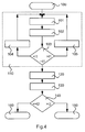
- FIG. 4 shows a flow chart of a discrimination method in accordance with the present invention,
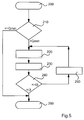
- FIG. 5 shows a flow diagram of a deletion method in accordance with the present invention, and
- FIG. 6 shows a block diagram of a memory device in accordance with the present invention.
- FIG. 3 shows a series of characteristics of cells all having different gains and a common point P1 identified by the co-ordinates V1,I1, i.e. by applying the reading voltage V1 to all these cells there is obtained therefrom the same reading current I1 and the characteristics are indicated in decreasing order of gain and threshold voltage by B0 (with gain G0 and threshold voltage VT(B0)), B1 (with gain G1 and threshold voltage VT(B1)), B2 (with gain G2 and threshold voltage VT(B2)) respectively. The voltages Vt0 and VT1 keep the same meaning explained above.
- The method in accordance with the present invention for discriminating on the basis of the gain a memory cell of the type with single insulated-gate memorisation transistor comprisEs the following phases:
- a. carry the insulated gate of the cell in a charge state such that by applying a first reading voltage V1 to the cell by means of successive programming and/or deletion and verification phases there is detected a first reading current about equal to a first value I1 (as shown in FIG. 3),
- b. apply a second reading voltage V2,
- c. detect a second reading current I(B) opposite the second reading voltage V2,
- d. compare the value of the second reading current I(B) with a second value I2 which together with the second reading voltage V2 identifies a point P2, and
- e. associate the cell alternatively with a first or a second class of cells based on the outcome of said comparison.
- Specifically for the purposes of the present invention it proved advantageous to have the second reading voltage V2, e.g. 6.25V, higher than the first reading voltage V1, e.g. 4.5V, the second value I2 higher than the first value I1, and the cell associated with a first class of high-gain cells if from said comparison it proved that said second reading current I(B) was higher than said second value I2 and otherwise with a second low-gain cell class.
- The discrimination method can be rapidly understood by considering the description made together with the flow chart shown in FIG. 4, having the following block-actions correspondence:
100 method start
110 cell conditioning - phase a. of the method
101 apply V1
102 detect I(V1)
103 test on I(V1) in relation to I1
104 deletion phase
105 programming phase
120 apply V2 - phase b. of the method
130 detect I(V2) - phase c. of the method
140 test on I(V2) in relation to I2 - phase d. of the method
150 high-gain association - end of method phase e.
160 low-gain association - end of method phase e. - The one shown in FIG. 3 could be the situation which appears in three cells of an EPROM flash memory device after phase a. of the method in accordance with the present invention. By applying to the three cells the second reading voltage V2 there will be detected the currents I(B0), I(B1), I(B2) respectively of which the first two are higher than the second value I2 while the last, i.e. I(B2), is not. For the purposes of the present method therefore the first three cells will be considered high-gain and the last low-gain. Graphically it can be seen that the characteristics slope reflects this situation.
- It is specified lastly that the real form of the cell characteristics is not the rectilinear type but their qualitative behaviour, for the purposes of the graph and method, is the same.
- It remains to be discussed how to perform practically in a physical memory device phase d. of the method, i.e. the current comparison. This can be done, e.g. by using a reference memory cell having the BRIF characteristic having a reference gain GRIF and brought to a threshold voltage VT(BRIF) such that by applying thereto the second reading voltage V2 the reading current I2 is detected, and sending to a sense amplifier the currents of the reference cell and of the cell to be discriminated. Current comparisons by means of sense amplifiers and reference cells are used normally in reading operations and in programming and deletion verification phases using appropriate reference cells. Thus to discriminate the cells on the basis of gain basically no further circuitry in the memory device is necessary.
- Since the low cell gain problem becomes, as explained above, particularly dangerous for the memory device when one prepares to delete it, the ideal moment for performance of a discrimination phase is concomitantly with the deletion operation.
- As explained above, a conventional deletion operation of the cells of a memory device of the insulated-gate single-transistor memorisation type, in particular the EPROM flash type, consists of at least one series of successive individual deletion and verification phases of the cell deletion status.
- The deletion method in accordance with the present invention comprises also at least one individual cell discrimination phase on the basis of the gain suitable for identifying the high-gain cells and provides that, after said discrimination phase, the individual verification phases affect only the high-gain cells.
- In this manner it is avoided that many cells be 'depleted'.
- The deletion method can be rapidly understood by considering the description given together with the flow chart shown in FIG. 5 and having the following block-actions correspondence and in which V3 and I3 indicate the voltage and current respectively on the basis of which the cell deletion condition is to be verified:
BlockAction
200 method start
210 gain test of cell G compared with Gmin
220 apply V3
230 detect I(V3)
240 test on I(V3) compared with I3
250 deletion phase
260 method end
In the example of FIG. 5 the discrimination phase - block 210 - precedes the actual cell deletion. - The discrimination phase can be provided by any method.
- It is particularly advantageous to use the discrimination method in accordance with the present invention immediately after the 'preconditioning' and before the actual deletion because in this case, if a value of V1 lower than the value of VT0 is chosen, the discrimination phase already carries a partial but not dangerous deletion of the cells which thus shortens the actual deletion. As a whole then the deletion performed with the method of the present invention is not basically longer than that of the known art but considerably safer.
- All these operations can affect the entire memory device or blocks thereof.
- The cells which are not high-gain are considered faulty and possibly signalled as such to the user of the device. In a very simple case the user will avoid using them.
- A more sophisticated version of the method provides that at least the faulty cells are replaced with redundant cells. More often it happens that the entire column or row to which they belong is replaced.
- In this last case, for reasons of uniformity of use of all the cells of the matrix, it is well that all the redundant cells experience on average the same life as the non-redundant cells before their replacement. To achieve this it is necessary that the preconditioning and subsequent deletion affect always also the redundant cells.
- It has been seen that various 'fault' phenomena affect the memory devices during their life and among these lowering of the cell gain.
- There is not explained with the aid of FIG. 6 the memory device in accordance with the present invention which is fault tolerant. It comprises:
- a.) matrix MAT of memory cells having a plurality of rows and columns of which at least one row and/or column RID is redundant,
- b.) decoding means RDEC,CDEC for row and/or column addresses, and
- c.) control logic CL for writing, reading and deletion of the cells and control of the device components.
- The decoding means RDEC, CDEC comprise at least one non-volatile memory NVM for address mapping and the control logic CL comprises means TST designed to identify cell faults in the rows and/or columns and writing means WM designed to write on the non-volatile memory NVM, during normal operation of the device, addresses corresponding to said at least one redundant row and/or column RID to rectify said faults.
- In the example of FIG. 6 there is a matrix MAT made up of 8 rows and 8 columns, only one redundant column RID, a 3-bit row decoder RDEC, a 3-bit column decoder CDEC, and a non-volatile memory NVM formed from 8 3-bit words, used only for mapping column addresses and included in the 3-bit column decoder CDEC.
- From the control logic CL comes out the column address to be sent to the 3-bit column decoder CDEC, the row address to be sent to the 3-bit row decoder RDEC, and at least one signal DEL for the deletion to be sent to the matrix MAT. Furthermore it is connected to the input of the 3-bit row decoder RDEC and the input of the 3-bit column decoder CDEC. The means TST pilot the writing means WM which are connected in writing to the non-volatile memory NVM.
- Initially the non-volatile memory NVM contains in order the following eight words: 000, 001, 010, 011, 100, 101, 110, 111.
- When the means TST identify a 'fault' among those foreseen in a particular cell, they send to the writing means WM the column address corresponding to said faulty cell, e.g. 011. The writing means WM use this address to address the non-volatile memory NVM and use as writing data the column address corresponding to the redundancy column, in the example 111, and perform a writing operation on the non-volatile memory NVM.
- At the end the non-volatile memory NVM contains in order the following eight words: 000, 001, 010, 111, 100, 101, 110, 111.
- In the example there is no possibility of rectifying additional 'faults'.
- The design and realization of such a control logic CL falls within the normal activities and abilities of those skilled in the art.
- It is clear that control of the entire device is entrusted to the control logic CL which can be the wired or programmed type. For deletion, this can be pre-set to operate in accordance with the method of the present invention.
- The means TST can be in particular individual discrimination means for the cells of the matrix MAT which can consist of logics of the wired or programmed type and operate, e.g. in accordance with the method of the present invention.
- A fault tolerant memory device in accordance with the present invention can find an advantageous application in any integrated circuit where it is necessary to store data and/or programs.
Claims (11)
- Method of discriminating a memory cell of the single-transistor insulated gate memorization type and in particular of the EPROM type based on gain and comprising the following phases:a) carry the insulated gate of the cell in a charge state such that by applying a first reading voltage (V1) to the cell by means of successive programming and/or deletion and verification phases there is detected a first reading current about equal to a first value (I1),b) apply a second reading voltage (V2),c) detect a second current (I(B)) opposite the second reading voltage (V2),d) compare the value of the second reading current (I(B)) with a second value (I2), ande) associate the cell alternatively with a first or a second class of cells based on the outcome of said comparison.
- Method in accordance with claim 1 in which said second reading voltage (V2) is higher than said first reading voltage (V1) and in which said second value (I2) is higher than said first value (I1) and in which said cell is associated with a first class of high-gain cells if from said comparison it proves that said second reading current (I(B)) is higher than said second value (I2) and otherwise is associated with a second class of low-gain cells.
- Method of deleting cells of a memory device of the single-transistor insulated gate memorisation type and in particular the EPROM flash type by means of at least one series of successive deletion and individual verification phases of the cell deletion state and characterised in that it comprises at least one individual discrimination phase of said cells on the basis of the gain designed to identify the high-gain cells and in that, after said discrimination phase, said individual verification phases affect only the high-gain cells.
- Method in accordance with claim 3 in which said discrimination phase takes place in accordance with the method set forth in claims 1 or 2 before said series of successive deletion and verification phases.
- Method in accordance with claim 3 or 4 in which the cells not high-gain are considered faulty.
- Method in accordance with claim 5 in which at least said faulty cells are replaced by redundant cells.
- Method in accordance with claim 6 in which said redundant cells experience on average the same life as the non-redundant cells before said replacement.
- Memory device, in particular flash EPROM, of the type comprising:a.) matrix (MAT) of memory cells having a plurality of rows and columns of which at least one row and/or column (RID) is redundant,b) decoding means RDEC,CDEC for row and/or column addresses, andc.) control logic (CL) for writing, reading and deletion of the cells and control of the device components,characterized in that said decoding means (RDEC,CDEC) comprise at least one non-volatile memory (NVM) for mapping said addresses and that said control logic (CL) comprises means (TST) designed to identify cell faults in said rows and/or columns and writing means (WM) designed to write on said non-volatile memory (NVM) during normal operation of said device addresses corresponding to said at least one redundant row and/or column (RID) to rectify said faults.
- Device in accordance with claim 8 in which said control logic (CL) comprises additionally discrimination means (TST) for said cells on the basis of gain and designed to pilot said writing means (WM),
- Device in accordance with claim 9 in which said control logic (CL) operates for deletion in accordance with the method set forth in one of the claims from 3 to 7.
- Integrated circuit comprising a memory device for storing data and/or programs characterised in that said memory device is the type set forth in claims 8 to 10.
Priority Applications (4)
| Application Number | Priority Date | Filing Date | Title |
|---|---|---|---|
| DE69426818T DE69426818T2 (en) | 1994-06-10 | 1994-06-10 | Fault-tolerant storage device, in particular of the "flash EEPROM" type |
| EP94830283A EP0686979B1 (en) | 1994-06-10 | 1994-06-10 | Failure tolerant memory device, in particular of the flash EEPROM type |
| US08/454,650 US5682349A (en) | 1994-06-10 | 1995-05-31 | Failure tolerant memory device, in particular of the flash EEPROM type |
| JP14503495A JP3725581B2 (en) | 1994-06-10 | 1995-06-12 | CELL DISCRIMINATION METHOD AND ERASE METHOD, MEMORY DEVICE USED FOR THEM, AND INTEGRATED CIRCUIT USING THE MEMORY DEVICE |
Applications Claiming Priority (1)
| Application Number | Priority Date | Filing Date | Title |
|---|---|---|---|
| EP94830283A EP0686979B1 (en) | 1994-06-10 | 1994-06-10 | Failure tolerant memory device, in particular of the flash EEPROM type |
Publications (2)
| Publication Number | Publication Date |
|---|---|
| EP0686979A1 true EP0686979A1 (en) | 1995-12-13 |
| EP0686979B1 EP0686979B1 (en) | 2001-03-07 |
Family
ID=8218466
Family Applications (1)
| Application Number | Title | Priority Date | Filing Date |
|---|---|---|---|
| EP94830283A Expired - Lifetime EP0686979B1 (en) | 1994-06-10 | 1994-06-10 | Failure tolerant memory device, in particular of the flash EEPROM type |
Country Status (4)
| Country | Link |
|---|---|
| US (1) | US5682349A (en) |
| EP (1) | EP0686979B1 (en) |
| JP (1) | JP3725581B2 (en) |
| DE (1) | DE69426818T2 (en) |
Cited By (3)
| Publication number | Priority date | Publication date | Assignee | Title |
|---|---|---|---|---|
| US6345367B1 (en) | 1996-07-11 | 2002-02-05 | Memory Corporation Plc | Defective memory block handling system by addressing a group of memory blocks for erasure and changing the content therewith |
| WO2005029504A2 (en) | 2003-09-17 | 2005-03-31 | Sandisk Corporation | Methods for identifying non-volatile memory elements with poor subthreshold slope or weak transconductance |
| WO2005093762A1 (en) * | 2004-03-01 | 2005-10-06 | Intel Corporation | Memory defect detection and self-repair technique |
Families Citing this family (9)
| Publication number | Priority date | Publication date | Assignee | Title |
|---|---|---|---|---|
| US6532556B1 (en) | 2000-01-27 | 2003-03-11 | Multi Level Memory Technology | Data management for multi-bit-per-cell memories |
| US6314023B1 (en) * | 2000-06-15 | 2001-11-06 | Motorola, Inc. | Non-volatile programming elements for redundancy and identification in an integrated circuit |
| US6466476B1 (en) | 2001-01-18 | 2002-10-15 | Multi Level Memory Technology | Data coding for multi-bit-per-cell memories having variable numbers of bits per memory cell |
| DE60212332T2 (en) * | 2002-04-26 | 2007-06-06 | Stmicroelectronics S.R.L., Agrate Brianza | Self-repair method for non-volatile memory with error-avoidance architecture and non-volatile memory |
| DE60230592D1 (en) | 2002-05-21 | 2009-02-12 | St Microelectronics Srl | Self-repair method for nonvolatile memory device with erase / program error detection, and nonvolatile memory device therefor |
| US6839275B2 (en) * | 2003-06-04 | 2005-01-04 | Hewlett-Packard Development Company, L.P. | Memory system having control circuit configured to receive data, provide encoded received data to match a fault pattern in the array of memory cells |
| JP2006294144A (en) * | 2005-04-12 | 2006-10-26 | Toshiba Corp | Nonvolatile semiconductor memory device |
| EP1947539A4 (en) * | 2005-09-27 | 2011-05-18 | Advantest Corp | Control method, and control system |
| US7545679B1 (en) * | 2007-12-28 | 2009-06-09 | Freescale Semiconductor, Inc. | Electrical erasable programmable memory transconductance testing |
Citations (9)
| Publication number | Priority date | Publication date | Assignee | Title |
|---|---|---|---|---|
| US4733394A (en) * | 1985-04-23 | 1988-03-22 | Deutsche Itt Industries Gmbh | Electrically programmable semiconductor memory showing redundance |
| US4779272A (en) * | 1985-11-13 | 1988-10-18 | Mitsubishi Denki Kabushiki Kaisha | Testable variable-threshold non-volatile semiconductor memory |
| EP0403822A1 (en) * | 1989-06-19 | 1990-12-27 | Texas Instruments Incorporated | Circuit and method for conditioning erased eeproms prior to programming |
| GB2254173A (en) * | 1991-02-11 | 1992-09-30 | Intel Corp | Row redundancy for flash memories |
| DE4207934A1 (en) * | 1991-03-12 | 1992-10-01 | Toshiba Kawasaki Kk | ELECTRICALLY LOAD AND PROGRAMMABLE NON-VOLATILE STORAGE SYSTEM WITH WRITE-PRUEF ADJUSTMENT USING TWO REFERENCE LEVELS |
| EP0548866A2 (en) * | 1991-12-27 | 1993-06-30 | Nec Corporation | Non-volatile semiconductor memory device |
| FR2694404A1 (en) * | 1992-07-31 | 1994-02-04 | Sgs Thomson Microelectronics | Integrated memory cell threshold voltage measurement method esp. for EPROM or FLASH EPROM - comparing current in transistor with two reference currents, using read amplifier |
| WO1994007211A2 (en) * | 1992-09-21 | 1994-03-31 | Sundisk Corporation | Latent defect handling in eeprom devices |
| EP0600151A2 (en) * | 1992-12-03 | 1994-06-08 | Fujitsu Limited | Nonvolatile semiconductor memory device having electrically and collectively erasable characteristics |
Family Cites Families (2)
| Publication number | Priority date | Publication date | Assignee | Title |
|---|---|---|---|---|
| KR960002777B1 (en) * | 1992-07-13 | 1996-02-26 | 삼성전자주식회사 | Row redundancy device for a semiconductor device |
| JP3212421B2 (en) * | 1993-09-20 | 2001-09-25 | 富士通株式会社 | Nonvolatile semiconductor memory device |
-
1994
- 1994-06-10 DE DE69426818T patent/DE69426818T2/en not_active Expired - Fee Related
- 1994-06-10 EP EP94830283A patent/EP0686979B1/en not_active Expired - Lifetime
-
1995
- 1995-05-31 US US08/454,650 patent/US5682349A/en not_active Expired - Lifetime
- 1995-06-12 JP JP14503495A patent/JP3725581B2/en not_active Expired - Lifetime
Patent Citations (9)
| Publication number | Priority date | Publication date | Assignee | Title |
|---|---|---|---|---|
| US4733394A (en) * | 1985-04-23 | 1988-03-22 | Deutsche Itt Industries Gmbh | Electrically programmable semiconductor memory showing redundance |
| US4779272A (en) * | 1985-11-13 | 1988-10-18 | Mitsubishi Denki Kabushiki Kaisha | Testable variable-threshold non-volatile semiconductor memory |
| EP0403822A1 (en) * | 1989-06-19 | 1990-12-27 | Texas Instruments Incorporated | Circuit and method for conditioning erased eeproms prior to programming |
| GB2254173A (en) * | 1991-02-11 | 1992-09-30 | Intel Corp | Row redundancy for flash memories |
| DE4207934A1 (en) * | 1991-03-12 | 1992-10-01 | Toshiba Kawasaki Kk | ELECTRICALLY LOAD AND PROGRAMMABLE NON-VOLATILE STORAGE SYSTEM WITH WRITE-PRUEF ADJUSTMENT USING TWO REFERENCE LEVELS |
| EP0548866A2 (en) * | 1991-12-27 | 1993-06-30 | Nec Corporation | Non-volatile semiconductor memory device |
| FR2694404A1 (en) * | 1992-07-31 | 1994-02-04 | Sgs Thomson Microelectronics | Integrated memory cell threshold voltage measurement method esp. for EPROM or FLASH EPROM - comparing current in transistor with two reference currents, using read amplifier |
| WO1994007211A2 (en) * | 1992-09-21 | 1994-03-31 | Sundisk Corporation | Latent defect handling in eeprom devices |
| EP0600151A2 (en) * | 1992-12-03 | 1994-06-08 | Fujitsu Limited | Nonvolatile semiconductor memory device having electrically and collectively erasable characteristics |
Cited By (10)
| Publication number | Priority date | Publication date | Assignee | Title |
|---|---|---|---|---|
| US6345367B1 (en) | 1996-07-11 | 2002-02-05 | Memory Corporation Plc | Defective memory block handling system by addressing a group of memory blocks for erasure and changing the content therewith |
| WO2005029504A2 (en) | 2003-09-17 | 2005-03-31 | Sandisk Corporation | Methods for identifying non-volatile memory elements with poor subthreshold slope or weak transconductance |
| WO2005029504A3 (en) * | 2003-09-17 | 2005-09-01 | Sandisk Corp | Methods for identifying non-volatile memory elements with poor subthreshold slope or weak transconductance |
| US7046555B2 (en) | 2003-09-17 | 2006-05-16 | Sandisk Corporation | Methods for identifying non-volatile memory elements with poor subthreshold slope or weak transconductance |
| US7414894B2 (en) | 2003-09-17 | 2008-08-19 | Sandisk Corporation | Methods for identifying non-volatile memory elements with poor subthreshold slope or weak transconductance |
| EP2015310A3 (en) * | 2003-09-17 | 2009-04-15 | SanDisk Corporation | Methods for identifying non-volatile memory elements with poor subthreshold slope or weak transconductance |
| CN1853241B (en) * | 2003-09-17 | 2011-10-12 | 桑迪士克股份有限公司 | Methods for identifying non-volatile memory elements with poor subthreshold slope or weak transconductance |
| KR101124175B1 (en) * | 2003-09-17 | 2012-03-27 | 가부시끼가이샤 도시바 | Methods for identifying non-volatile memory elements with poor subthreshold slope or weak transconductance |
| WO2005093762A1 (en) * | 2004-03-01 | 2005-10-06 | Intel Corporation | Memory defect detection and self-repair technique |
| US7177189B2 (en) | 2004-03-01 | 2007-02-13 | Intel Corporation | Memory defect detection and self-repair technique |
Also Published As
| Publication number | Publication date |
|---|---|
| DE69426818D1 (en) | 2001-04-12 |
| JPH0883500A (en) | 1996-03-26 |
| DE69426818T2 (en) | 2001-10-18 |
| JP3725581B2 (en) | 2005-12-14 |
| EP0686979B1 (en) | 2001-03-07 |
| US5682349A (en) | 1997-10-28 |
Similar Documents
| Publication | Publication Date | Title |
|---|---|---|
| EP0314180B1 (en) | Nonvolatile semiconductor memory having a stress test circuit | |
| US7437631B2 (en) | Soft errors handling in EEPROM devices | |
| US5532962A (en) | Soft errors handling in EEPROM devices | |
| JP2807203B2 (en) | Electrically programmable memory and method of writing data to memory | |
| US7457168B2 (en) | Non-volatile memory device and associated method of erasure | |
| KR0168896B1 (en) | Semiconductor memory of xn type having error correcting circuit by parity | |
| JP3450625B2 (en) | Nonvolatile semiconductor memory device and operation method thereof | |
| US5590075A (en) | Method for testing an electrically erasable and programmable memory device | |
| US6563752B2 (en) | Qualification test method and circuit for a non-volatile memory | |
| DE102007016460A1 (en) | Non-volatile memory device, non-volatile memory system and reading method for a nonvolatile memory device | |
| EP0686979B1 (en) | Failure tolerant memory device, in particular of the flash EEPROM type | |
| US20070025167A1 (en) | Method for testing a memory device, test unit for testing a memory device and memory device | |
| JPH06267300A (en) | Nonvolatile semiconductor memory device, semiconductor device and testing method therefor | |
| WO1981000154A1 (en) | Programmable read only memory integrated circuit with bitcheck and deprogramming modes and methods for programming and testing said circuit | |
| US6819589B1 (en) | Flash memory with pre-detection for data loss | |
| US20080285368A1 (en) | Method for nrom array word line retry erasing and threshold voltage recovering | |
| US6735733B2 (en) | Method for the correction of a bit in a string of bits | |
| JP4467371B2 (en) | Nonvolatile semiconductor memory device and method for setting replacement information of nonvolatile semiconductor memory device | |
| JP4251717B2 (en) | Nonvolatile semiconductor memory device | |
| KR970017698A (en) | Method of replacing semiconductor memory device and redundant memory cell unit | |
| US5594693A (en) | Matrix device with redundancy fuses for integrated memory | |
| US20040218421A1 (en) | Non-volatile memory having a bias on the source electrode for HCI programming | |
| US5715195A (en) | Programmable memory verify "0" and verify "1" circuit and method | |
| US20080002452A1 (en) | Method for setting a read voltage, and semiconductor circuit arrangement | |
| US5561635A (en) | PROM IC enabling a stricter memory cell margin test |
Legal Events
| Date | Code | Title | Description |
|---|---|---|---|
| PUAI | Public reference made under article 153(3) epc to a published international application that has entered the european phase |
Free format text: ORIGINAL CODE: 0009012 |
|
| AK | Designated contracting states |
Kind code of ref document: A1 Designated state(s): DE FR GB IT |
|
| 17P | Request for examination filed |
Effective date: 19960601 |
|
| 17Q | First examination report despatched |
Effective date: 19980529 |
|
| RAP3 | Party data changed (applicant data changed or rights of an application transferred) |
Owner name: STMICROELECTRONICS S.R.L. |
|
| GRAG | Despatch of communication of intention to grant |
Free format text: ORIGINAL CODE: EPIDOS AGRA |
|
| GRAG | Despatch of communication of intention to grant |
Free format text: ORIGINAL CODE: EPIDOS AGRA |
|
| GRAH | Despatch of communication of intention to grant a patent |
Free format text: ORIGINAL CODE: EPIDOS IGRA |
|
| GRAH | Despatch of communication of intention to grant a patent |
Free format text: ORIGINAL CODE: EPIDOS IGRA |
|
| GRAA | (expected) grant |
Free format text: ORIGINAL CODE: 0009210 |
|
| STAA | Information on the status of an ep patent application or granted ep patent |
Free format text: STATUS: THE PATENT HAS BEEN GRANTED |
|
| AK | Designated contracting states |
Kind code of ref document: B1 Designated state(s): DE FR GB IT |
|
| REF | Corresponds to: |
Ref document number: 69426818 Country of ref document: DE Date of ref document: 20010412 |
|
| ET | Fr: translation filed | ||
| ITF | It: translation for a ep patent filed |
Owner name: BOTTI & FERRARI S.R.L. |
|
| REG | Reference to a national code |
Ref country code: GB Ref legal event code: IF02 |
|
| PLBE | No opposition filed within time limit |
Free format text: ORIGINAL CODE: 0009261 |
|
| 26N | No opposition filed | ||
| PGFP | Annual fee paid to national office [announced via postgrant information from national office to epo] |
Ref country code: DE Payment date: 20030610 Year of fee payment: 10 |
|
| PGFP | Annual fee paid to national office [announced via postgrant information from national office to epo] |
Ref country code: GB Payment date: 20040602 Year of fee payment: 11 |
|
| PGFP | Annual fee paid to national office [announced via postgrant information from national office to epo] |
Ref country code: FR Payment date: 20040628 Year of fee payment: 11 |
|
| PG25 | Lapsed in a contracting state [announced via postgrant information from national office to epo] |
Ref country code: DE Free format text: LAPSE BECAUSE OF NON-PAYMENT OF DUE FEES Effective date: 20050101 |
|
| PG25 | Lapsed in a contracting state [announced via postgrant information from national office to epo] |
Ref country code: IT Free format text: LAPSE BECAUSE OF NON-PAYMENT OF DUE FEES;WARNING: LAPSES OF ITALIAN PATENTS WITH EFFECTIVE DATE BEFORE 2007 MAY HAVE OCCURRED AT ANY TIME BEFORE 2007. THE CORRECT EFFECTIVE DATE MAY BE DIFFERENT FROM THE ONE RECORDED. Effective date: 20050610 Ref country code: GB Free format text: LAPSE BECAUSE OF NON-PAYMENT OF DUE FEES Effective date: 20050610 |
|
| PG25 | Lapsed in a contracting state [announced via postgrant information from national office to epo] |
Ref country code: FR Free format text: LAPSE BECAUSE OF NON-PAYMENT OF DUE FEES Effective date: 20060228 |
|
| GBPC | Gb: european patent ceased through non-payment of renewal fee |
Effective date: 20050610 |
|
| REG | Reference to a national code |
Ref country code: FR Ref legal event code: ST Effective date: 20060228 |