EP0670549A2 - High availability data processing system and method using finite state machines - Google Patents
High availability data processing system and method using finite state machines Download PDFInfo
- Publication number
- EP0670549A2 EP0670549A2 EP94480148A EP94480148A EP0670549A2 EP 0670549 A2 EP0670549 A2 EP 0670549A2 EP 94480148 A EP94480148 A EP 94480148A EP 94480148 A EP94480148 A EP 94480148A EP 0670549 A2 EP0670549 A2 EP 0670549A2
- Authority
- EP
- European Patent Office
- Prior art keywords
- memory
- data storage
- data
- storage locations
- coupled
- Prior art date
- Legal status (The legal status is an assumption and is not a legal conclusion. Google has not performed a legal analysis and makes no representation as to the accuracy of the status listed.)
- Withdrawn
Links
Images
Classifications
-
- G—PHYSICS
- G06—COMPUTING; CALCULATING OR COUNTING
- G06F—ELECTRIC DIGITAL DATA PROCESSING
- G06F11/00—Error detection; Error correction; Monitoring
- G06F11/07—Responding to the occurrence of a fault, e.g. fault tolerance
- G06F11/16—Error detection or correction of the data by redundancy in hardware
- G06F11/20—Error detection or correction of the data by redundancy in hardware using active fault-masking, e.g. by switching out faulty elements or by switching in spare elements
- G06F11/202—Error detection or correction of the data by redundancy in hardware using active fault-masking, e.g. by switching out faulty elements or by switching in spare elements where processing functionality is redundant
- G06F11/2038—Error detection or correction of the data by redundancy in hardware using active fault-masking, e.g. by switching out faulty elements or by switching in spare elements where processing functionality is redundant with a single idle spare processing component
-
- G—PHYSICS
- G06—COMPUTING; CALCULATING OR COUNTING
- G06F—ELECTRIC DIGITAL DATA PROCESSING
- G06F11/00—Error detection; Error correction; Monitoring
- G06F11/07—Responding to the occurrence of a fault, e.g. fault tolerance
- G06F11/08—Error detection or correction by redundancy in data representation, e.g. by using checking codes
-
- G—PHYSICS
- G06—COMPUTING; CALCULATING OR COUNTING
- G06F—ELECTRIC DIGITAL DATA PROCESSING
- G06F11/00—Error detection; Error correction; Monitoring
- G06F11/07—Responding to the occurrence of a fault, e.g. fault tolerance
- G06F11/16—Error detection or correction of the data by redundancy in hardware
- G06F11/20—Error detection or correction of the data by redundancy in hardware using active fault-masking, e.g. by switching out faulty elements or by switching in spare elements
-
- G—PHYSICS
- G06—COMPUTING; CALCULATING OR COUNTING
- G06F—ELECTRIC DIGITAL DATA PROCESSING
- G06F11/00—Error detection; Error correction; Monitoring
- G06F11/07—Responding to the occurrence of a fault, e.g. fault tolerance
- G06F11/0703—Error or fault processing not based on redundancy, i.e. by taking additional measures to deal with the error or fault not making use of redundancy in operation, in hardware, or in data representation
- G06F11/0751—Error or fault detection not based on redundancy
- G06F11/0763—Error or fault detection not based on redundancy by bit configuration check, e.g. of formats or tags
-
- G—PHYSICS
- G06—COMPUTING; CALCULATING OR COUNTING
- G06F—ELECTRIC DIGITAL DATA PROCESSING
- G06F11/00—Error detection; Error correction; Monitoring
- G06F11/07—Responding to the occurrence of a fault, e.g. fault tolerance
- G06F11/16—Error detection or correction of the data by redundancy in hardware
- G06F11/20—Error detection or correction of the data by redundancy in hardware using active fault-masking, e.g. by switching out faulty elements or by switching in spare elements
- G06F11/202—Error detection or correction of the data by redundancy in hardware using active fault-masking, e.g. by switching out faulty elements or by switching in spare elements where processing functionality is redundant
- G06F11/2023—Failover techniques
- G06F11/2028—Failover techniques eliminating a faulty processor or activating a spare
-
- G—PHYSICS
- G06—COMPUTING; CALCULATING OR COUNTING
- G06F—ELECTRIC DIGITAL DATA PROCESSING
- G06F2201/00—Indexing scheme relating to error detection, to error correction, and to monitoring
- G06F2201/86—Event-based monitoring
Landscapes
- Engineering & Computer Science (AREA)
- Theoretical Computer Science (AREA)
- Quality & Reliability (AREA)
- Physics & Mathematics (AREA)
- General Engineering & Computer Science (AREA)
- General Physics & Mathematics (AREA)
- Maintenance And Management Of Digital Transmission (AREA)
- Error Detection And Correction (AREA)
- Detection And Prevention Of Errors In Transmission (AREA)
Abstract
The invention is a high availability data processing system. It includes a primary processor at a first node of a communications network with a serial data stream, having failure detection logic therein, for outputting an alarm signal to the network having a characteristic pattern indicating a failure in the primary processor. The invention further includes a first standby processor at a second node of the communications network, having a first event driven interface therein coupled to the network, for detecting the alarm signal. When the characteristic pattern is detected by the event driven interface, switch over logic in the first standby processor, invokes primary status in the first standby processor.
Description
- The invention relates to data processing systems and more particularly relates to a system and method for high availability data processing, using finite state machines.
- Finite state machines (FSM) are commonly used in the implementation of telecommunications protocols and of input/output processors, because finite state machines can define all possible conditions completely and unambiguously. However, a problem with finite state machines is defining the sequence of states and the accompanying actions to be accomplished with each state. Convention implementations of finite state machines result in program code sets which are extensive and complex. This problem has been solved by the "System and Method for Adaptive, Active Monitoring of a Serial Data Stream having a Characteristic Pattern," by Paul C. Hershey, et al., cited above. The adaptive, active monitor comprises finite state machines (FSM) which are constructed to detect the occurrence of a characteristic data pattern in a bit stream. If the FSM successfully detects the pattern, it then outputs a pattern alarm signal, indicating the successful detection of the characteristic data pattern.
- One feature of the adaptive, active monitor invention is the programmability of the finite state machines (FSMs) and the programmability of their interconnection. Each FSM consists of an address register and a memory. The address register has two portions, an n-X bit wide first portion and a X-bit wide second portion. X is one bit for binary data, X is a word of two bits for Manchester encoded data, or X is a word of five bits for FDDI encoded data. The X-bit wide portion is connected to the input data stream which contains the characteristic data pattern of interest. The n-X bit wide portion contains data which is output from the memory. The next address to be applied by the address register to the memory is made up of the n-X bit wide portion and the next arriving X-bit word from the input data stream.
- Each memory has a plurality of data storage locations, each having a first portion with n-X bits, to be output to the address register as part of the next address. Many of the memory locations have a second portion which stores a command to reset the address register if the FSM fails to detect its designated component bit pattern.
- A terminal location in the memory of an FSM will include a start signal value to signal another FSM to start analyzing the data stream. If the terminal location in a predecessor FSM memory is successful in matching the last bit of its designated component bit pattern, then it will output a starting signal to a succeeding FSM. The succeeding FSM will begin analyzing the data stream for the next component bit pattern of the characteristic data pattern. The memory of an FSM can be a writable RAM, enabling its reconfiguration to detect different component bit patterns.
- A long standing problem in data processing technology is the provision of highly reliable systems for continuous availability of the data processing resource. Redundant systems have been configured in the prior art, to provide a standby processor to take the place of a primary processor when the primary fails. Various techniques have been used to initiate the switchover of the standby processor. The standby may be running the same program as the primary, in synchronism with the primary, but the standby generates no outout. The standby monitors a heartbeat signal from the primary, to periodically check the health of the primary. If the standby senses that the primary is failing, the standby will switchover to perform the functions of the primary, generating the output that had been generated by the primary. The control of the swithover can be initiated by the standby signalling the primary to stop, while the standby takes over the primary's functions. This is known as a hot-standby configuration.
- The problem with this prior art approach to high availability, is that the control of the monitoring of the heartbeat and the switchover is done by a sequence of programmed instructions. The execution of the programmed instructions takes time, and therefore the swithover action must wait until the monitoring program completes its execution and issues the control signal to begin the switchover operation. The prior art hot-standby configurations are not sufficiently fast to permit high speed, high availability data processing in critical applications.
- It is therefore an object of the invention to increase the speed of detection of a characteristic failure data pattern from the primary processor, to obtain effective, realtime control for high speed, hot-standby data processing systems.
- It is another object of the invention to provide high speed, programmable finite state machines to detect characteristic failure data patterns from the primary processor.
- It is another object of the invention to detect characteristic failure data patterns in a high speed data processing system.
- The invention is a high availability data processing system. It includes a primary processor at a first node of a communications network with a serial data stream, having failure detection logic therein, for outputting an alarm signal to the network having a characteristic pattern indicating a failure in the primary processor.
- The invention further includes a first standby processor at a second node of the communications network, having a first event driven interface therein coupled to the network, for detecting the alarm signal.
- The invention further includes a first n-bit address register in the first event driven interface, having a first portion with n-x bits and a second portion with a plurality of x bits and an input of the second portion coupled to the serial stream, for receiving x-bit words from the serial data stream.
- The invention further includes first addressable memory having a plurality of data storage locations, each having a first portion with n-x bits, the first memory having an n-bit address input coupled an output of the first address register, the first memory configured with data stored in first and second ones of the data storage locations to represent a digital filter for the characteristic alarm pattern.
- The invention further includes a feedback path from an output of the first memory to an input of the first register, for transferring the data from the first one of the data storage locations in the first memory to the first portion of the first address register, for concatenation with the x-bit words from the serial data stream to form an address for the second one of the data storage locations of the first memory.
- The invention further includes the second one of the data storage locations of the first memory having a switch over signal value stored therein, which is output when the characteristic pattern is detected by the digital filter.
- The invention further includes switch over logic in the first standby processor, coupled to the second data storage location, for invoking primary status in the first standby processor.
- Further in accordance with the invention, it can include a second standby processor at a third node of the communications network, having a second event driven interface therein coupled to the network, for detecting the alarm signal.
- The invention further includes a second n-bit address register in the second event driven interface, having a first portion with n-x bits and a second portion with a plurality of x bits and an input of the second portion thereof coupled to the serial stream, for receiving x-bit words from the serial data stream.
- The invention further includes second addressable memory having a plurality of data storage locations, each having a first portion with n-x bits, the second memory having an n-bit address input coupled an output of the second address register, the second memory configured with data stored in first and second ones of the data storage locations therein to represent a digital filter for the characteristic alarm pattern.
- The invention further includes a feedback path from an output of the second memory to an input of the second register, for transferring the data from the first one of the data storage locations in the second memory to the first portion of the second address register, for concatenation with the x-bit words from the serial data stream to form an address for the second one of the data storage locations of the second memory.
- The invention further includes the second one of the data storage locations of the second memory having a standby activation signal value stored therein, which is output when the characteristic pattern is detected by the digital filter thereof.
- The invention further includes activation logic in the second standby processor, coupled to the second data storage location in the second memory, for invoking hot standby status in the second standby processor.
- Further in accordance with the invention, the primary processor includes a system bus coupled to a data processing element that outputs a failure signal to the system bus having a second characteristic pattern, indicating a failure in the data processing
The invention further includes the primary processor having a second event driven interface therein coupled to the system bus, for detecting the failure signal. - The invention further includes a second n-bit address register in the second event driven interface, having a first portion with n-x bits and a second portion with a plurality of x bits and an input of the second portion thereof coupled to the system bus, for receiving x-bit words from the system bus.
- The invention further includes second addressable memory having a plurality of data storage locations, each having a first portion with n-x bits, the second memory having an n-bit address input coupled an output of the second address register, the second memory configured with data stored in first and second ones of the data storage locations therein to represent a digital filter for the second characteristic failure pattern.
- The invention further includes a feedback path from an output of the second memory to an input of the second register, for transferring the data from the first one of the data storage locations in the second memory to the first portion of the second address register, for concatenation with the x-bit words from the serial data stream to form an address for the second one of the data storage locations of the second memory.
- The invention further includes the second one of the data storage locations of the second memory having a failure detection signal value stored therein, which is output when the second characteristic pattern is detected by the digital filter thereof.
- The invention further includes the failure detection logic in the primary processor, coupled to the second data storage location in the second memory, for transmitting the alarm signal to the network, in response to the failure detection signal value.
- The invention can further include failure correction logic in the primary processor, coupled to the second data storage location in the second memory, for generating correction signals in response to the failure detection signal value, for correcting the failure in the data processing element.
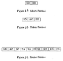
- Figs. 1A, 1B and 1C show three of the basic formats used in token rings; namely, abort, token, and frame.
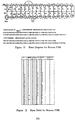
- Fig. 2 is the state diagram and regular expression that recognizes a Beacon MAC frame for the IEEE 802.5 token ring protocol.
- Fig. 3 shows the corresponding state table for a Beacon MAC frame.
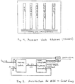
- Fig. 4 shows a configuration of adapters for an RS6000 computer that serves as the primary work station.
- Fig. 5 shows the architecture for using the event driven interface (ICA) to correct errors.
- The invention is a high availability data processing system. It includes a primary processor at a first node of a communications network with a serial data stream, having failure detection logic therein, for outputting an alarm signal to the network having a characteristic pattern indicating a failure in the primary processor. The invention further incudes a first standby processor at a second node of the communications network, having a first event driven interface therein coupled to the network, for detecting the alarm signal. When the characteristic pattern is detected by the event driven interface, switch over logic in the first standby processor, invokes primary status in the first standby processor.
- In this section we present an example of a failure detection capability for a characteristic pattern that indicates a failure on an IEEE 802.5 token ring network (1). For the IEEE 802.5 protocol, the data include LLC frame data and MAC frame data. LLC frame data include user data, source and destination addresses, and control field overhead. MAC frame data include data that control the operation of the token ring network and any ring station operations that affect the ring. Such data are required while the network is preparing to transmit data. Examples of MAC frames include nearest neighbor notification and beacons.
- The IEEE 802.5 token ring standard includes 4 channel symbols {J, K, 0, 1} (2). Unique strings of these symbols compose three of the basic formats used in token rings; namely, abort, token, and frame. We show these formats in Figs. 1A, 1B, and 1C. The following notation is used to delineate the fields within these formats: SD denotes the starting delimiter (comprising 1 octet), AC denotes the access control field (comprising 1 octet), FC denotes the frame control field (comprising 1 octet), DA denotes the destination address (comprising 2 or 6 octets), SA denotes the source address (comprising 2 or 6 octets), INFO denotes the information field (comprising between 0 and 17800 octets\cite{Tokarch '89}), FCS denotes the frame check sequence field (comprising 4 octets), ED denotes the ending delimiter (comprising 1 octet), and FS denotes the frame status field (comprising 1 octet).
- By detecting specific strings of channel symbols within these fields, one can identify characteristic patterns indicating a failure on the token ring network. For example, a hard fault is a permanent fault that causes the token ring to stop operating within the normal token ring protocol. Examples of hard faults include a broken cable or a jabbering station (2). A ring station downstream from the hard fault recognizes a hard error and transmits a Beacon MAC frame. A Beacon MAC frame identifies the beaconing ring station's nearest active upstream neighbor (NAUN) and the type of error detected.
- When the beaconing ring station's NAUN has copied eight Beacon MAC frames, the NAUN removes itself from the ring and tests itself and the ring (1). If the test is successful, the NAUN reattaches itself to the ring. If the test fails, the NAUN notifies the LAN manager. If the ring does not recover after a specified period of time, the beaconing station assumes that its NAUN has completed self-test, and the beaconing station removes itself from the ring for self-test. If the test is successful, the beaconing station notifies the LAN manager. If the ring still does not recover, the error cannot be corrected automatically, and manual intervention is required.
- The event driven interface (also referred to as the ICA) detects the characteristic pattern for a Beacon MAC frame. In Fig. 2 we present the state diagram and regular expression that recognizes a Beacon MAC frame for the IEEE 802.5 token ring protocol. The regular expression identifies the specific channel symbol sequences that compose a Beacon MAC frame. A sequence (X) followed by a * {e.g., (JKO)*} describes the set of possible symbol sequences that can be formed by concatenating a finite number of strings of symbols from (X) (3). In Fig. 3 we present the corresponding state table for a Beacon MAC frame.
- In this section we present an example of a failure detection capability for a characteristic pattern that indicates a failure on the system bus of an RS6000 computer (4). An RS6000 computer implements the Micro Channel Architecture. This architecture includes a system bus called the Micro Channel. The Micro Channel consists of a data bus, an address bus, an arbitration bus, a set of interrupts, and support signals. Micro Channel participants are either masters or slaves. A master drives the address bus and data transfer control signals that cause data transfer to or from a slave. A master can be a system master, bus master, or a DMA controller. A slave sends and receives data under the control of a master. A slave can be any adapter card.
- An exception condition is an event that disrupts the normal processing by a master. Exception conditions include: channel data and address parity exceptions, channel non-parity exceptions, master and slave dependent exceptions, catastrophic exceptions, and channel-timeout exceptions.
- A master reports exceptions with an interrupt and termination of bus ownership. A slave or channel monitor reports exceptions by activating a synchronous -CHCK signal. If - CHCK is activated, the system master or a bus master suspends processing and generates an interrupt. The interrupt invokes a utility program to handle the exception condition. In order to activate -CHCK, a slave sets
bit 7 of POS register 5 to a 0. This indicates the source of the exception in all cases except address parity errors. The ICA device can detectbit 7 of POS register 5 and issue an alarm instantaneously. This alarm can invoke the utility program to handle the exception condition. Therefore, the ICA can replace the exception handling function of the master with a real-time capability. A possible configuration of adapters for an RS6000 computer that server as the primary work station is shown in Fig. 4. - In Fig. 5 we present an architecture for using the ICA to correct errors. The Address Latches operates accepts the input data from the channel as well as the feedback address bits output for the RAM lookup table. The RAM lookup table includes the error detection finite state machine as well as the error correction finite state machine. Consider the example of a simple error-correcting code consider a code with 4 valid code words:
0000000000 0001111000 1110000111 1111111111.
This code can correct two errors. If a symbol sequence arrives with a value of 1100000011, the finite state machine implemented within the RAM detects an error an outputs an error alarm. The RAM finite state machine then implements a decoder that decodes this word to the closest valid code word, (e.g., 1110000111). The error alarm signal is sent to control logic multiplexer (mux). If there is an error alarm, then the code word from the RAM is passed through the mux. If there is no error, then the original code word is passed through the mux. -
- 1. IBM Corp., Token-Ring Network Architecture Reference, Research Triangle Park, NC, 1989.
- 2. IEEE, Inc., IEEE Standard 802.5, Token Ring Access Method, New York, NY, 1989.
- 3. Z. ∼Kohavi, Switching and Finite Automata Theory, McGraw-Hill, New York, NY, 1978.
- 4. IBM, RISC System/6000 Power Station and Power Server Hardware Technical Reference Micro Channel Architecture, Raleigh, NC, 1990.
Claims (5)
- A high availability data processing system, comprising:
a primary processor at a first node of a communications network with a serial data stream, having failure detection logic therein, for outputting an alarm signal to said network having a characteristic pattern indicating a failure in said primary processor;
a first standby processor at a second node of said communications network, having a first event driven interface therein coupled to said network, for detecting said alarm signal;
a first n-bit address register in said first event driven interface, having a first portion with n-x bits and a second portion with a plurality of x bits and an input of said second portion coupled to said serial stream, for receiving x-bit words from said serial data stream;
first addressable memory having a plurality of data storage locations, each having a first portion with n-x bits, said first memory having an n-bit address input coupled an output of said first address register, said first memory configured with data stored in first and second ones of said data storage locations to represent a digital filter for said characteristic alarm pattern;
a feedback path from an output of said first memory to an input of said first register, for transferring said data from said first one of said data storage locations in said first memory to said first portion of said first address register, for concatenation with said x-bit words from said serial data stream to form an address for said second one of said data storage locations of said first memory;
said second one of said data storage locations of said first memory having a switch over signal value stored therein, which is output when said characteristic pattern is detected by said digital filter;
switch over logic in said first standby processor, coupled to said second data storage location, for invoking primary status in said first standby processor. - The data processing system of claim 1, which further comprises:
a second standby processor at a third node of said communications network, having a second event driven interface therein coupled to said network, for detecting said alarm signal;
a second n-bit address register in said second event driven interface, having a first portion with n-x bits and a second portion with a plurality of x bits and an input of said second portion thereof coupled to said serial stream, for receiving x-bit words from said serial data stream;
second addressable memory having a plurality of data storage locations, each having a first portion with n-x bits, said second memory having an n-bit address input coupled an output of said second address register, said second memory configured with data stored in first and second ones of said data storage locations therein to represent a digital filter for said characteristic alarm pattern;
a feedback path from an output of said second memory to an input of said second register, for transferring said data from said first one of said data storage locations in said second memory to said first portion of said second address register, for concatenation with said x-bit words from said serial data stream to form an address for said second one of said data storage locations of said second memory;
said second one of said data storage locations of said second memory having a standby activation signal value stored therein, which is output when said characteristic pattern is detected by said digital filter thereof;
activation logic in said second standby processor, coupled to said second data storage location in said second memory, for invoking hot standby status in said second standby processor. - The data processing system of claim 1, wherein said primary processor includes a system bus coupled to a data processing element that outputs a failure signal to said system bus having a second characteristic pattern, indicating a failure in said data processing element, said primary processor further comprising:
said primary processor having a second event driven interface therein coupled to said system bus, for detecting said failure signal;
a second n-bit address register in said second event driven interface, having a first portion with n-x bits and a second portion with a plurality of x bits and an input of said second portion thereof coupled to said system bus, for receiving x-bit words from said system bus;
second addressable memory having a plurality of data storage locations, each having a first portion with n-x bits, said second memory having an n-bit address input coupled an output of said second address register, said second memory configured with data stored in first and second ones of said data storage locations therein to represent a digital filter for said second characteristic failure pattern;
a feedback path from an output of said second memory to an input of said second register, for transferring said data from said first one of said data storage locations in said second memory to said first portion of said second address register, for concatenation with said x-bit words from said serial data stream to form an address for said second one of said data storage locations of said second memory;
said second one of said data storage locations of said second memory having a failure detection signal value stored therein, which is output when said second characteristic pattern is detected by said digital filter thereof;
said failure detection logic in said primary processor, coupled to said second data storage location in said second memory, for transmitting said alarm signal to said network, in response to said failure detection signal value. - The data processing system of claim 3, which further comprises:
failure correction logic in said primary processor, coupled to said second data storage location in said second memory, for generating correction signals in response to said failure detection signal value, for correcting said failure in said data processing element. - A method for providing high availability in a data processing system, comprising:
outputting an alarm signal from a primary processor at a first node of a communications network with a serial data stream, said processor having failure detection logic therein, for said alarm signal sent to said network having a characteristic pattern indicating a failure in said primary processor;
detecting said alarm signal in a first standby processor at a second node of said communications network, having a first event driven interface therein coupled to said network, for detecting said alarm signal;
receiving a first n-bit address register in said first event driven interface, having a first portion with n-x bits and a second portion with a plurality of x bits and an input of said second portion coupled to said serial stream, said first register receiving x-bit words from said serial data stream;
storing in a first addressable memory having a plurality of data storage locations, each having a first portion with n-x bits, said first memory having an n-bit address input coupled an output of said first address register, said first memory configured with data stored in first and second ones of said data storage locations to represent a digital filter for said characteristic alarm pattern;
transferring in a feedback path from an output of said first memory to an input of said first register, for transferring said data from said first one of said data storage locations in said first memory to said first portion of said first address register, for concatenation with said x-bit words from said serial data stream to form an address for said second one of said data storage locations of said first memory;
outputting from said second one of said data storage locations of said first memory having a switch over signal value stored therein, which is output when said characteristic pattern is detected by said digital filter; and
invoking with switch over logic in said first standby processor, coupled to said second data storage location, for invoking primary status in said first standby processor.
Applications Claiming Priority (2)
| Application Number | Priority Date | Filing Date | Title |
|---|---|---|---|
| US184098 | 1994-01-19 | ||
| US08/184,098 US5544077A (en) | 1994-01-19 | 1994-01-19 | High availability data processing system and method using finite state machines |
Publications (1)
| Publication Number | Publication Date |
|---|---|
| EP0670549A2 true EP0670549A2 (en) | 1995-09-06 |
Family
ID=22675538
Family Applications (1)
| Application Number | Title | Priority Date | Filing Date |
|---|---|---|---|
| EP94480148A Withdrawn EP0670549A2 (en) | 1994-01-19 | 1994-11-24 | High availability data processing system and method using finite state machines |
Country Status (3)
| Country | Link |
|---|---|
| US (1) | US5544077A (en) |
| EP (1) | EP0670549A2 (en) |
| JP (1) | JP2728119B2 (en) |
Families Citing this family (43)
| Publication number | Priority date | Publication date | Assignee | Title |
|---|---|---|---|---|
| JPH1011369A (en) * | 1996-06-27 | 1998-01-16 | Hitachi Ltd | Communication system and information processor with hot standby switching function |
| US5883939A (en) * | 1996-08-29 | 1999-03-16 | Cornell Research Foundation, Inc. | Distributed architecture for an intelligent networking coprocessor |
| US6393581B1 (en) | 1996-08-29 | 2002-05-21 | Cornell Research Foundation, Inc. | Reliable time delay-constrained cluster computing |
| US5933474A (en) * | 1996-12-24 | 1999-08-03 | Lucent Technologies Inc. | Telecommunications call preservation in the presence of control failure and high processing load |
| US6128734A (en) * | 1997-01-17 | 2000-10-03 | Advanced Micro Devices, Inc. | Installing operating systems changes on a computer system |
| US5875290A (en) * | 1997-03-27 | 1999-02-23 | International Business Machines Corporation | Method and program product for synchronizing operator initiated commands with a failover process in a distributed processing system |
| US6012150A (en) * | 1997-03-27 | 2000-01-04 | International Business Machines Corporation | Apparatus for synchronizing operator initiated commands with a failover process in a distributed processing system |
| US6154754A (en) * | 1997-09-25 | 2000-11-28 | Siemens Corporate Research, Inc. | Automatic synthesis of semantic information from multimedia documents |
| IL124187A (en) * | 1998-04-23 | 2001-10-31 | Dspc Israel Ltd | π/4 QPSK MODULATOR |
| US6425092B1 (en) | 1998-06-17 | 2002-07-23 | International Business Machines Corporation | Method and apparatus for preventing thermal failure in a semiconductor device through redundancy |
| US6134690A (en) * | 1998-06-25 | 2000-10-17 | Cisco Technology, Inc. | Computerized automation system and method |
| JP2000035928A (en) * | 1998-07-16 | 2000-02-02 | Yazaki Corp | Network monitor system and method therefor |
| US6169726B1 (en) * | 1998-12-17 | 2001-01-02 | Lucent Technologies, Inc. | Method and apparatus for error free switching in a redundant duplex communication carrier system |
| US6553401B1 (en) | 1999-07-09 | 2003-04-22 | Ncr Corporation | System for implementing a high volume availability server cluster including both sharing volume of a mass storage on a local site and mirroring a shared volume on a remote site |
| KR100324275B1 (en) * | 1999-07-14 | 2002-02-25 | 서평원 | Dual State Control Method Of Duplicated Processors |
| US6526524B1 (en) * | 1999-09-29 | 2003-02-25 | International Business Machines Corporation | Web browser program feedback system |
| WO2001027717A2 (en) * | 1999-10-11 | 2001-04-19 | I2 Technologies, Inc. | Distributed session services |
| JP3651353B2 (en) * | 2000-04-04 | 2005-05-25 | 日本電気株式会社 | Digital content reproduction system and digital content distribution system |
| US7389332B1 (en) | 2001-09-07 | 2008-06-17 | Cisco Technology, Inc. | Method and apparatus for supporting communications between nodes operating in a master-slave configuration |
| US7260741B2 (en) * | 2001-09-18 | 2007-08-21 | Cedar Point Communications, Inc. | Method and system to detect software faults |
| US7421478B1 (en) | 2002-03-07 | 2008-09-02 | Cisco Technology, Inc. | Method and apparatus for exchanging heartbeat messages and configuration information between nodes operating in a master-slave configuration |
| US6948008B2 (en) * | 2002-03-12 | 2005-09-20 | Intel Corporation | System with redundant central management controllers |
| US7200610B1 (en) | 2002-04-22 | 2007-04-03 | Cisco Technology, Inc. | System and method for configuring fibre-channel devices |
| US7433952B1 (en) | 2002-04-22 | 2008-10-07 | Cisco Technology, Inc. | System and method for interconnecting a storage area network |
| US7165258B1 (en) * | 2002-04-22 | 2007-01-16 | Cisco Technology, Inc. | SCSI-based storage area network having a SCSI router that routes traffic between SCSI and IP networks |
| US7587465B1 (en) * | 2002-04-22 | 2009-09-08 | Cisco Technology, Inc. | Method and apparatus for configuring nodes as masters or slaves |
| US7415535B1 (en) | 2002-04-22 | 2008-08-19 | Cisco Technology, Inc. | Virtual MAC address system and method |
| US7188194B1 (en) | 2002-04-22 | 2007-03-06 | Cisco Technology, Inc. | Session-based target/LUN mapping for a storage area network and associated method |
| US7240098B1 (en) | 2002-05-09 | 2007-07-03 | Cisco Technology, Inc. | System, method, and software for a virtual host bus adapter in a storage-area network |
| US20040054943A1 (en) * | 2002-08-08 | 2004-03-18 | International Business Machines Corporation | Method and system for improving the availability of software processes utilizing configurable finite state tables |
| US7213724B1 (en) * | 2003-01-15 | 2007-05-08 | Langer David S | Table tennis ball delivery device |
| US7831736B1 (en) | 2003-02-27 | 2010-11-09 | Cisco Technology, Inc. | System and method for supporting VLANs in an iSCSI |
| US7295572B1 (en) | 2003-03-26 | 2007-11-13 | Cisco Technology, Inc. | Storage router and method for routing IP datagrams between data path processors using a fibre channel switch |
| JP4155399B2 (en) * | 2003-03-28 | 2008-09-24 | 株式会社日立製作所 | Computer processing method, its execution system, and its processing program |
| US7904599B1 (en) | 2003-03-28 | 2011-03-08 | Cisco Technology, Inc. | Synchronization and auditing of zone configuration data in storage-area networks |
| US7433300B1 (en) | 2003-03-28 | 2008-10-07 | Cisco Technology, Inc. | Synchronization of configuration data in storage-area networks |
| US7526527B1 (en) | 2003-03-31 | 2009-04-28 | Cisco Technology, Inc. | Storage area network interconnect server |
| US7451208B1 (en) | 2003-06-28 | 2008-11-11 | Cisco Technology, Inc. | Systems and methods for network address failover |
| KR20070083760A (en) * | 2004-10-25 | 2007-08-24 | 로베르트 보쉬 게엠베하 | Method and device for switching in a computer system having at least two execution units |
| US7281070B2 (en) * | 2005-01-28 | 2007-10-09 | International Business Machines Corporation | Multiple master inter integrated circuit bus system |
| US7583590B2 (en) * | 2005-07-15 | 2009-09-01 | Telefonaktiebolaget L M Ericsson (Publ) | Router and method for protocol process migration |
| CN101169623B (en) * | 2007-11-22 | 2010-07-07 | 东北大学 | Non-linear procedure fault identification method based on kernel principal component analysis contribution plot |
| CN105911977B (en) * | 2016-04-22 | 2018-10-26 | 浙江大学 | The method for diagnosing faults that nested iterations Fei Sheer discriminant analyses are combined with opposite variation |
Family Cites Families (45)
| Publication number | Priority date | Publication date | Assignee | Title |
|---|---|---|---|---|
| US3638193A (en) * | 1970-02-02 | 1972-01-25 | Bell Telephone Labor Inc | {62 -element switching network control |
| US4227245A (en) * | 1972-06-01 | 1980-10-07 | Westinghouse Electric Corp. | Digital computer monitored system or process which is configured with the aid of an improved automatic programming system |
| US3806647A (en) * | 1972-07-28 | 1974-04-23 | Communications Satellite Corp | Phase ambiguity resolution system using convolutional coding-threshold decoding |
| US4063038A (en) * | 1975-11-24 | 1977-12-13 | Digital Communications Corporation | Error coding communication terminal interface |
| US4162480A (en) * | 1977-01-28 | 1979-07-24 | Cyclotomics, Inc. | Galois field computer |
| JPS6043550B2 (en) * | 1980-10-28 | 1985-09-28 | 日本電気株式会社 | Communication line control device |
| US4445171A (en) * | 1981-04-01 | 1984-04-24 | Teradata Corporation | Data processing systems and methods |
| JPS5840924A (en) * | 1981-09-03 | 1983-03-10 | Nippon Telegr & Teleph Corp <Ntt> | Encoder |
| JPS5854755A (en) * | 1981-09-28 | 1983-03-31 | Nippon Telegr & Teleph Corp <Ntt> | Decoding device |
| US4521849A (en) * | 1981-10-01 | 1985-06-04 | Honeywell Information Systems Inc. | Programmable hit matrices used in a hardware monitoring interface unit |
| US4458309A (en) * | 1981-10-01 | 1984-07-03 | Honeywell Information Systems Inc. | Apparatus for loading programmable hit matrices used in a hardware monitoring interface unit |
| US4459656A (en) * | 1981-10-01 | 1984-07-10 | Honeywell Information Systems Inc. | Clocking system for a computer performance monitoring device |
| US4466098A (en) * | 1982-06-11 | 1984-08-14 | Siemens Corporation | Cross channel circuit for an electronic system having two or more redundant computers |
| JPS5981738A (en) * | 1982-11-01 | 1984-05-11 | Fujitsu Ltd | State control system |
| US4660196A (en) * | 1983-08-01 | 1987-04-21 | Scientific Atlanta, Inc. | Digital audio satellite transmission system |
| US4709365A (en) * | 1983-10-31 | 1987-11-24 | Beale International Technology Limited | Data transmission system and method |
| JPH0710069B2 (en) * | 1984-08-23 | 1995-02-01 | 日本電信電話株式会社 | Packet communication system |
| US4805089A (en) * | 1985-04-30 | 1989-02-14 | Prometrix Corporation | Process control interface system for managing measurement data |
| US4779194A (en) * | 1985-10-15 | 1988-10-18 | Unisys Corporation | Event allocation mechanism for a large data processing system |
| US5062055A (en) * | 1986-09-02 | 1991-10-29 | Digital Equipment Corporation | Data processor performance advisor |
| US4980824A (en) * | 1986-10-29 | 1990-12-25 | United Technologies Corporation | Event driven executive |
| CA1280217C (en) * | 1987-06-01 | 1991-02-12 | Stephen R.H. Hardy | Method and apparatus for utilization of dual latency stations for performance improvement of token ring networks |
| US4851998A (en) * | 1987-06-03 | 1989-07-25 | I/O Xel, Inc. | Method for analyzing performance of computer peripherals |
| JPS6427334A (en) * | 1987-07-22 | 1989-01-30 | Mitsubishi Electric Corp | Duplex switching system |
| US4958273A (en) * | 1987-08-26 | 1990-09-18 | International Business Machines Corporation | Multiprocessor system architecture with high availability |
| US4887076A (en) * | 1987-10-16 | 1989-12-12 | Digital Equipment Corporation | Computer interconnect coupler for clusters of data processing devices |
| US4905171A (en) * | 1987-11-09 | 1990-02-27 | International Business Machines Corporation | Workstation controller performance monitor |
| US5434998A (en) * | 1988-04-13 | 1995-07-18 | Yokogawa Electric Corporation | Dual computer system |
| US5072376A (en) * | 1988-06-10 | 1991-12-10 | Amdahl Corporation | Measuring utilization of processor shared by multiple system control programs |
| US5035302A (en) * | 1989-03-03 | 1991-07-30 | Otis Elevator Company | "Artificial Intelligence" based learning system predicting "Peak-Period" times for elevator dispatching |
| US5067107A (en) * | 1988-08-05 | 1991-11-19 | Hewlett-Packard Company | Continuous computer performance measurement tool that reduces operating system produced performance data for logging into global, process, and workload files |
| US4939724A (en) * | 1988-12-29 | 1990-07-03 | Intel Corporation | Cluster link interface for a local area network |
| JP2804125B2 (en) * | 1989-11-08 | 1998-09-24 | 株式会社日立製作所 | Fault monitoring device and control method for information processing system |
| EP0431232A1 (en) * | 1989-12-06 | 1991-06-12 | International Business Machines Corporation | Mechanism for measuring the service times of software and hardware components in complex systems |
| US5079760A (en) * | 1990-02-06 | 1992-01-07 | Paul Nemirovsky | Method for efficient distributed data communications network access network configuration |
| US5307481A (en) * | 1990-02-28 | 1994-04-26 | Hitachi, Ltd. | Highly reliable online system |
| JPH0413338A (en) * | 1990-05-01 | 1992-01-17 | Mitsubishi Electric Corp | Specific bit content detection circuit |
| US5220668A (en) * | 1990-09-21 | 1993-06-15 | Stratus Computer, Inc. | Digital data processor with maintenance and diagnostic system |
| US5132962A (en) * | 1990-12-20 | 1992-07-21 | International Business Machines Corporation | Fault isolation and bypass reconfiguration unit |
| JPH07507893A (en) * | 1992-06-12 | 1995-08-31 | ザ、ダウ、ケミカル、カンパニー | Security front-end communication system and method for process control computers |
| JPH0612288A (en) * | 1992-06-29 | 1994-01-21 | Hitachi Ltd | Information processing system and monitoring method therefor |
| US5365514A (en) * | 1993-03-01 | 1994-11-15 | International Business Machines Corporation | Event driven interface for a system for monitoring and controlling a data communications network |
| US5375070A (en) * | 1993-03-01 | 1994-12-20 | International Business Machines Corporation | Information collection architecture and method for a data communications network |
| US5390326A (en) * | 1993-04-30 | 1995-02-14 | The Foxboro Company | Local area network with fault detection and recovery |
| US5406504A (en) * | 1993-06-30 | 1995-04-11 | Digital Equipment | Multiprocessor cache examiner and coherency checker |
-
1994
- 1994-01-19 US US08/184,098 patent/US5544077A/en not_active Expired - Fee Related
- 1994-11-24 EP EP94480148A patent/EP0670549A2/en not_active Withdrawn
- 1994-12-27 JP JP6324185A patent/JP2728119B2/en not_active Expired - Lifetime
Also Published As
| Publication number | Publication date |
|---|---|
| US5544077A (en) | 1996-08-06 |
| JPH07221739A (en) | 1995-08-18 |
| JP2728119B2 (en) | 1998-03-18 |
Similar Documents
| Publication | Publication Date | Title |
|---|---|---|
| US5544077A (en) | High availability data processing system and method using finite state machines | |
| KR930007903B1 (en) | Digital equipment frame removal mechanism for token ring corporation networks | |
| US5041963A (en) | Local area network with an active star topology comprising ring controllers having ring monitor logic function | |
| EP0196911B1 (en) | Local area networks | |
| US9030943B2 (en) | Recovering from failures without impact on data traffic in a shared bus architecture | |
| US7010612B1 (en) | Universal serializer/deserializer | |
| JPH0624371B2 (en) | Communication control device | |
| JP2713226B2 (en) | Automatic IP address generation method in network | |
| EP0137438B1 (en) | Method for passing a token in a local-area network | |
| US20070242611A1 (en) | Computer Hardware Fault Diagnosis | |
| EP0471354A2 (en) | Intelligent network interface circuit | |
| JPS60148249A (en) | Message removing method | |
| JPH0339422B2 (en) | ||
| US5528594A (en) | Method and system for implementing sub-tokens on a token ring network | |
| KR100194366B1 (en) | Pattern injector | |
| US5363493A (en) | Token ring network test device using finite state machine | |
| JPH0691538B2 (en) | Packet end signal generator | |
| JPH0666806B2 (en) | Token ring transmission method | |
| US5191655A (en) | Interface arrangement for facilitating data communication between a computer and peripherals | |
| JPH03140038A (en) | Token ring net work recovery method and device therefor | |
| JPH03204258A (en) | Fault detection system, transmission line reconstitution system and communication system | |
| JP2502465B2 (en) | Master-adapter device | |
| EP0725514A1 (en) | Port address resolution device | |
| EP1476986B1 (en) | Information communication controller interface apparatus and method | |
| Ibbett et al. | Centrenet–A High Performance Local Area Network |
Legal Events
| Date | Code | Title | Description |
|---|---|---|---|
| PUAI | Public reference made under article 153(3) epc to a published international application that has entered the european phase |
Free format text: ORIGINAL CODE: 0009012 |
|
| AK | Designated contracting states |
Kind code of ref document: A2 Designated state(s): DE FR GB |
|
| 17P | Request for examination filed |
Effective date: 19951115 |
|
| STAA | Information on the status of an ep patent application or granted ep patent |
Free format text: STATUS: THE APPLICATION HAS BEEN WITHDRAWN |
|
| 18W | Application withdrawn |
Withdrawal date: 19961015 |