EP0614209A1 - A flat panel display - Google Patents
A flat panel display Download PDFInfo
- Publication number
- EP0614209A1 EP0614209A1 EP94301384A EP94301384A EP0614209A1 EP 0614209 A1 EP0614209 A1 EP 0614209A1 EP 94301384 A EP94301384 A EP 94301384A EP 94301384 A EP94301384 A EP 94301384A EP 0614209 A1 EP0614209 A1 EP 0614209A1
- Authority
- EP
- European Patent Office
- Prior art keywords
- screen
- sheet
- electron
- electrons
- flat panel
- Prior art date
- Legal status (The legal status is an assumption and is not a legal conclusion. Google has not performed a legal analysis and makes no representation as to the accuracy of the status listed.)
- Withdrawn
Links
Images


Classifications
-
- H—ELECTRICITY
- H01—ELECTRIC ELEMENTS
- H01J—ELECTRIC DISCHARGE TUBES OR DISCHARGE LAMPS
- H01J31/00—Cathode ray tubes; Electron beam tubes
- H01J31/08—Cathode ray tubes; Electron beam tubes having a screen on or from which an image or pattern is formed, picked up, converted, or stored
- H01J31/10—Image or pattern display tubes, i.e. having electrical input and optical output; Flying-spot tubes for scanning purposes
- H01J31/12—Image or pattern display tubes, i.e. having electrical input and optical output; Flying-spot tubes for scanning purposes with luminescent screen
- H01J31/123—Flat display tubes
- H01J31/125—Flat display tubes provided with control means permitting the electron beam to reach selected parts of the screen, e.g. digital selection
- H01J31/127—Flat display tubes provided with control means permitting the electron beam to reach selected parts of the screen, e.g. digital selection using large area or array sources, i.e. essentially a source for each pixel group
Definitions
- the present invention relates generally to a video display and more particularly to a flat panel display.
- One prior art approach for a flat panel display has a flat phosphor screen set at a high voltage and multiple layers of insulated metallic grids set at low voltages. Electrons emitted from sources are modulated by the low voltages on the metallic grids as they propagate through the grids, and are accelerated by the high voltage to form images on the screen.
- the intervening metallic grids serve as focusing structures. Unfortunately, it is expensive and difficult to reliably make and align multiple layers of insulated metallic grids with small enough apertures for high resolution images.
- Another prior art approach uses dynamically varying voltages applied onto phosphor stripes on a screen. This is known as the switched-anode technique.
- the sources commonly used for such an approach are field emission cathodes which are solid state electron-emitters controlled by gates.
- field emission cathodes which are solid state electron-emitters controlled by gates.
- a general discussion on field emission cathodes can be found in "Physical properties of thin-film field emission cathodes with molybdenum cones," written by C.A. Spindt et. al.
- the screen is located very close to the gates of the field emission cathodes without any intervening focusing grid structures. A number of positive voltages on the numerous phosphor stripes attract the electrons from the sources to form images on the screen.
- the potentials on the screen are comparable in magnitude to the potentials on the gates. This implies that the potential differences between the screen and the gates are low leading to electrons reaching the screen with low energy; this in turn reduces the electron-to-light conversion efficiency of the display.
- images usually vary dynamically. This requires a dynamically varying voltage for each stripe on the screen. Again, to prevent voltage breakdown, the electric fields between adjacent stripes cannot be too high. The fixed voltage difference between adjacent pixels limits the distance between stripes which in turn limits the resolution of the display.
- the present invention provides a low cost, high resolution flat panel display that is reliable, efficient and easy to manufacture. Its pixel resolution is high with excellent image contrast.
- the display has a high electron-to-light conversion efficiency and a high power efficiency.
- a preferred embodiment of the invented display generates an image on a screen by means of an electron source and an aperture in a sheet of material.
- the sheet is positioned between the electron source and the screen which emits visible light to form images when struck by electrons.
- the electrons pass through the aperture when they move from the electron source toward the screen.
- the screen and the sheet are at different potentials so that the aperture in the sheet functions as an electron-optical lens guiding a substantial amount of the electrons from the source to form the image on the screen of the flat panel display.
- Figure 1 shows a cross-sectional view of a preferred embodiment of the invention.
- Figures 2A-C shows equipotential surfaces established in the preferred embodiment.
- Figure 3 is a ray-tracing diagram illustrating the electron paths from an electron source in the preferred embodiment.
- Figures 4A-D depict different cross-sectional structures for the sheet of material in the preferred embodiment.
- Figure 5 shows a cross-sectional view of the preferred embodiment with two electron sources.
- Figure 6 illustrates a cross-sectional view of the preferred embodiment with three electron sources for a color display.
- Figures 7A-B show the top views of two different apertures, each with numerous electron sources in the preferred embodiment of the invention.
- Figures 8A-B illustrate cross-sectional views of two different types of electrodes to further guide the electrons in the preferred embodiment.
- Figure 9 shows another preferred embodiment of the invention with a curved screen.
- Figures 10A-B shows different views of a working embodiment of the invention.
- Figure 11 shows the top view of a part of the sheet of material with four apertures in the working embodiment.
- Figures 12A-B show different positions of a pair of focusing electrodes relative to an aperture in the working embodiment.
- FIG. 13 shows another working embodiment of the invention.
- Figures 14A-B depict two types of field emission cathodes for the working embodiments.
- the present invention provides a low cost, high resolution flat panel display that is reliable, efficient and easy to manufacture.
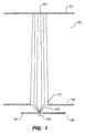
- Figure 1 shows a cross-sectional view of a preferred embodiment of the invented display 100.
- a screen 104 preferably a phosphor screen, is spaced apart from an electron source 106.
- a sheet of material 108 defines an aperture 112 through which a substantial amount of electrons 126 emitted by the electron source 106 travels to reach the screen 104.
- the electron source 106 preferably comprises a field emission cathode including an electron-emitter 109 and a gate 107 that modulates the number of electrons emitted by the emitter 109.
- a potential difference is established between the screen 104 and the sheet 108 so that the aperture 112 in the sheet 108 functions as an electron-optical lens.
- This lens guides the electrons 126 from the electron source 106 to strike the screen 104, causing the screen 104 to emit visible light in the form of an image 102.
- Figure 2A shows the aperture in the sheet functioning as an electron-optical lens 123 in the preferred embodiment of the invention.
- the voltage applied to the screen 104 is significantly more positive than the voltage applied to the sheet 108.
- the potential difference set up between the screen 104 and the sheet 108 establishes a plurality of equipotential surfaces 122.
- Figure 2B shows equipotential surfaces 151 in the vicinity of the aperture 112 of the electron-optical lens 123. Those surfaces 151 characterize the case in which the voltage level at the sheet 108 is between the voltage level at the screen 104 and the gate 107 of the electron source 106.
- Figure 2C shows equipotential surfaces 153 in the vicinity of the aperture 112 when the voltage level at the sheet 108 is lower than both the voltage level at the screen 104 and the gate 107.
- FIG. 3 is a ray-tracing diagram illustrating the electron paths from the electron source 106.
- the electron-optical lens 123 has a focal length f, 179, defining a focal point 175. This is the point where parallel rays converge.
- x (f/M)
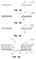
- Figures 4A-D depict different cross-sectional structures for the sheet of material in the preferred embodiment.
- Figure 4A shows the sheet 108A being a sheet of metal 200.
- Figure 4B illustrates the sheet 108B with a piece of metal 208 on both sides of a piece of insulator 206.
- Figure 4C shows the sheet 108C being a piece of metal 212 on one surface 214 of a piece of insulator 216.
- the sheet of material does not have to be thin relative to the distance 183 from the top surface of the sheet of material to the gate of the source.
- Figure 4D shows the preferred embodiment of the invention in which the sheet of material extends to the gate 107 of the source 106.
- the wall 203 of the sheet of material 108D does not have to be perpendicular to the plane of the sheet of material; the wall can define an oblique angle with respect to the plane.
- a piece of insulator is preferably formed at the surface of the sheet adjacent to the gate 107. This prevents the gate 107 from forming conductive paths with the sheet of material; for example, the surface 204 of the sheet 108D is insulated by a piece of insulator 201 from the gate 107.
- the aperture 112 in the sheet of material 108 is easy and inexpensive to make.
- the display For an average size display, such as 6'' by 8'', with VGA resolution (640 pixels by 480 pixels), the display has hundreds of thousands of pixels.
- VGA resolution 640 pixels by 480 pixels
- the simplicity in structure of the sheet of material in the present invention reduces the cost and the complexity while increases the reliability of making the display.
- the sheet 108 captures electrons travelling along undesirable directions from the electron source 106. An electron emitted at an angle that misses the aperture 112 is blocked by the sheet 108 so the sheet limits the divergence angle of the electrons emitted from the source 106.
- the sheet 108 may be used as the patterning mask for phosphor depositions in the same manner as conventional Cathode-Ray-Tubes. This helps to ensure color registration between the electron sources and the phosphor on the screen using matured technologies developed for CRTs.
- the display 100 has large number of pixels, sharp edge resolution, and excellent color saturation.
- the number of pixels on a display depends on the aperture size and the spacing between apertures. It is not difficult to make a 10'' * 10'' sheet of metal with a thickness of about 50 microns, and with apertures about 80 microns wide and about 300 microns apart to produce a display capable of VGA resolution.
- the sharp edge resolution of the image 102 is due to the sheet limiting the divergence angle of the electrons. Only electrons travelling along paths that are within the aperture reach the screen 104. With a substantially collimated electron beam 182, the boundary of the aperture 112 serves as a sharp demarcation for the image 102.
- the image 102 also has excellent color saturation because a significant amount of electrons are focused to each pixel without exciting adjacent pixels which usualiy are for different colors.
- the present invention has a high electron-to-light conversion efficiency and a high power efficiency. This is because the source 106 is close to the aperture 112, and the potential difference between the screen 104 and the sheet of material 108 is high relative to the potential difference between the sheet of material 108 and the gate 107. These characteristics lead to a significant amount of the emitted electrons reaching the aperture 112 to be accelerated to the screen 104. With a high potential difference between the screen and the sheet of material, the energy of the electrons is high when they reach the screen. This leads to a high electron-to-light conversion efficiency.
- the electrons that do not reach the screen are either captured by the sheet of material 108 or the gate 107.
- the voltages on the gate and the sheet are significantly lower than the voltage on the screen.
- power defined as voltage * current the electrons captured by the sheet and the gate lead to wasting very little power. So the display has a high power efficiency especially in comparison to the display using the switched-anode technique.
- Figure 5 shows a cross-sectional view of the preferred embodiment with two electron sources 250, 252 next to each other for one aperture 112.
- the sources are positioned so that a substantial amount of the electrons from the two sources are again guided by the electron-optical lens to form on the screen 104 two images 254, 256 which are substantially separate from each other.
- Figure 6 illustrates three electron sources 275, 277, 279 next to each other for a color display 287.
- the sources are positioned so that a substantial amount of the electrons from the sources are guided by the electron-optical lens to form on the screen three substantially separate images 281, 283, 285.
- the three collimated beams of electrons 291, 293, 295 strike onto three pixels on the screen 104.
- Each pixel has a different phosphor so that the three phosphors generate the three primary colors.
- modulating each of the sources one can generate all the colors from the three primary colors on the screen 104.
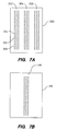
- Figure 7A shows the top view of an aperture 300 in a sheet of material with three groups of electron sources 302, 304, 306; for example, the group 302 has sources 308, 312 and 314. Each group enhances the image of and is adjacent to each source in Figure 6.
- Figure 7B shows the top view of an aperture 316 in a sheet of material with one group 318 of electron sources to enhance the image of and is adjacent to the source in Figure 1. At least 30% of the electrons emitted from each group of electron sources are guided by the electron-optical lens in their corresponding display to their screen.
- the numerous electron sources in each group provide an image with even intensity and reduce the noise level of the image through the averaging effect of the numerous electron sources.
- Figures 7A and 7B show rectangular apertures, this invention does not limit the apertures to be rectangular in shape.
- Figures 8A-B illustrate two different types of electrodes to further guide the electrons.
- Figure 8A shows a pair of focusing electrodes 325, 327 generally with a low voltage to focus the electrons towards their corresponding image.
- One preferred position of the electrodes is next to the electron source 329.
- Such electrodes are applied to both a single source and to a group of sources.
- Figure 8B shows a pair of steering electrodes 350, 352 to steer the collimated beam 354 from the pixel 356 to the pixel 358 on the screen 360.
- the invention reduces the number of electron sources with their electronic drivers by a factor of three for the display.
- the steering electrodes for all the apertures can be tied together under only one electronic controller. Although for each aperture, the beam is steered to the same color, whether different pixels on the screen show that color or not depends on whether the electron sources corresponding to those pixels are turned on. With the beams steered faster than 60 Hz, a viewer does not see any fluctuation in color. Such electrodes are applied to both a single source and to a group of sources.
- the focusing electrodes shown in Figure 8A is also capable of steering the beam
- the steering electrodes shown in Figure 8B is also capable of focusing the beam.
- FIG. 9 shows another preferred embodiment of the invention 362 with a curved screen 364.
- the image on the screen is relatively insensitive to the separation between the screen and the sheet. This is a desirable feature because the invention becomes applicable to a screen that is curved which is structurally stronger and can withstand higher pressure than a flat screen.
- Figures 10A-B show different views of a working embodiment 400 of the invention.
- Figure 10A shows the screen 401, the sheet of material 408 with numerous apertures and a substrate 410 with numerous field emission cathodes.
- FIG 10B shows a part of the cross-sectional view A-A of the display shown in Figure 10A.
- the screen 401 has numerous pixels, for example, 402, 404 and 405, which are about 100 microns apart and are formed as groups of three, a red pixel 402 next to a green pixel 404 which is next to a blue pixel 405.
- the distance 406 between the screen 401 and the sheet 408 is about 2 millimeters.
- the sheet 408 is a metal sheet with a thickness of about 50 microns.
- the distance 412 between the sheet 408 and the substrate 410 is about 100 microns.
- the substrate 410 has numerous field emission cathodes; for example, the cathode 440 with its electron-emitter 442 and its gate 409.
- the height of the electron-emitters is about 1 micron.
- On the substrate 410 there are also numerous focusing electrodes which are separated from the gates; for example, the focusing electrode 407, which is separated from the gate 409.
- the potential difference between the screen 401 and the sheet 408 is about 7000 volts
- between the sheet 408 and the gates 409 of field emission cathodes is about 100 volts
- between a gate and its focusing electrode is from 0 to ⁇ 100 volts
- between an electron-emitter and its gate is from 50 to 100 volts depending on the amount of electrons required to be emitted from the electron-emitter.
- Figure 11 shows the top view of a part of the sheet of material 408 with four apertures 425, 427, 429, 431 in the working embodiment 400.
- Each aperture is above three groups of field emission cathodes as in the aperture shown in Figure 7A; for example, the aperture 431 has the groups 441, 443, 445.
- the dimensions 435, 433 of each aperture are about 75 microns by 150 microns.
- the apertures are periodically spaced with periods of about 300 microns in both of its x, 437, and y, 439, directions.
- the focal length of the electron-optical lens is about 100 microns.
- the electron sources are positioned about 25 microns away from the focal point as described in equation 1.
- the expected resolution of the working embodiment is about 50 microns. With at least 60% of the electrons emitted by the sources expected to reach the screen, the display has an expected power efficiency of more than 99.5%. The minimum size of the display with VGA resolution is expected to be less than 5 inches.
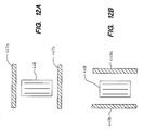
- Figures 12A-B show other preferred positions of a pair of focusing electrodes relative to an aperture.
- Figure 12A shows that the electrodes 447a and 447b are approximately perpendicular to the axis of the aperture 446
- Figure 12B shows that the electrodes 449a and 449b are approximately parallel to the axis of the aperture 448.
- the electrodes are preferably positioned on the substrate 410 or in between the substrate 410 and the sheet of material 408.
- Figure 13 shows another working embodiment 450 with the sheet of material 453 having apertures 457 extending across the whole sheet.
- the sheet of material with the long and narrow apertures can be formed by stretched-metal ribbons.
- Figures 14A-B show side views of two types of field emission cathodes.
- Figure 14A is a point source 475; it has a gate 477 and a cone 479 as the electron-emitter.
- Figure 14B is a field emission cathode 485 with a gate 487 and a line source 489 as the electron-emitter.
- the present invention provides a low cost, high resolution flat panel display that is reliable, efficient and easy to manufacture.
Landscapes
- Cathode-Ray Tubes And Fluorescent Screens For Display (AREA)
Abstract
A flat panel display (100, 362, 400, 450) with a screen (104), apertures (112) in a sheet of material (108) and electron sources (106). A potential difference is established between the screen (104) and the sheet (108). The electron sources (106) are positioned under the numerous apertures (112) which focus the electrons from the sources (106) to different positions on the screen (104). Additional electrodes (325, 350) are positioned in the display to further focus and steer the electrons toward the screen (104).
Description
- The present invention relates generally to a video display and more particularly to a flat panel display.
- One of the hurdles to reducing the cost, the size and the weight of a television or a computer is its display. Researchers have been trying for a long time to make a low cost and high resolution flat panel display that is reliable, efficient and easy to manufacture.
- One prior art approach for a flat panel display has a flat phosphor screen set at a high voltage and multiple layers of insulated metallic grids set at low voltages. Electrons emitted from sources are modulated by the low voltages on the metallic grids as they propagate through the grids, and are accelerated by the high voltage to form images on the screen. The intervening metallic grids serve as focusing structures. Unfortunately, it is expensive and difficult to reliably make and align multiple layers of insulated metallic grids with small enough apertures for high resolution images.
- Another prior art approach uses dynamically varying voltages applied onto phosphor stripes on a screen. This is known as the switched-anode technique. The sources commonly used for such an approach are field emission cathodes which are solid state electron-emitters controlled by gates. A general discussion on field emission cathodes can be found in "Physical properties of thin-film field emission cathodes with molybdenum cones," written by C.A. Spindt et. al. The screen is located very close to the gates of the field emission cathodes without any intervening focusing grid structures. A number of positive voltages on the numerous phosphor stripes attract the electrons from the sources to form images on the screen.
- With the screen very close to the gates, to prevent voltage breakdown, the potentials on the screen are comparable in magnitude to the potentials on the gates. This implies that the potential differences between the screen and the gates are low leading to electrons reaching the screen with low energy; this in turn reduces the electron-to-light conversion efficiency of the display.
- A significant number of the electrons do not reach the screen. They are collected by the gates. Since the potentials on the screen are comparable to the potentials on the gates, the fact that a significant number of electrons are collected by the gates implies wasting a significant percentage of the power. This leads to a low power efficiency display.
- Also, images usually vary dynamically. This requires a dynamically varying voltage for each stripe on the screen. Again, to prevent voltage breakdown, the electric fields between adjacent stripes cannot be too high. The fixed voltage difference between adjacent pixels limits the distance between stripes which in turn limits the resolution of the display.
- It will be apparent from the foregoing that there is still a need for a low cost and high resolution flat panel display that is reliable, efficient and easy to manufacture.
- The present invention provides a low cost, high resolution flat panel display that is reliable, efficient and easy to manufacture. Its pixel resolution is high with excellent image contrast. The display has a high electron-to-light conversion efficiency and a high power efficiency.
- A preferred embodiment of the invented display generates an image on a screen by means of an electron source and an aperture in a sheet of material. The sheet is positioned between the electron source and the screen which emits visible light to form images when struck by electrons. The electrons pass through the aperture when they move from the electron source toward the screen.
- The screen and the sheet are at different potentials so that the aperture in the sheet functions as an electron-optical lens guiding a substantial amount of the electrons from the source to form the image on the screen of the flat panel display.
- Other aspects and advantages of the present invention will become apparent from the following detailed description, taken in conjunction with the accompanying drawings, illustrating by way of example the principles of the invention.
- Figure 1 shows a cross-sectional view of a preferred embodiment of the invention.
- Figures 2A-C shows equipotential surfaces established in the preferred embodiment.
- Figure 3 is a ray-tracing diagram illustrating the electron paths from an electron source in the preferred embodiment.
- Figures 4A-D depict different cross-sectional structures for the sheet of material in the preferred embodiment.
- Figure 5 shows a cross-sectional view of the preferred embodiment with two electron sources.
- Figure 6 illustrates a cross-sectional view of the preferred embodiment with three electron sources for a color display.
- Figures 7A-B show the top views of two different apertures, each with numerous electron sources in the preferred embodiment of the invention.
- Figures 8A-B illustrate cross-sectional views of two different types of electrodes to further guide the electrons in the preferred embodiment.
- Figure 9 shows another preferred embodiment of the invention with a curved screen.
- Figures 10A-B shows different views of a working embodiment of the invention.
- Figure 11 shows the top view of a part of the sheet of material with four apertures in the working embodiment.
- Figures 12A-B show different positions of a pair of focusing electrodes relative to an aperture in the working embodiment.
- Figure 13 shows another working embodiment of the invention.
- Figures 14A-B depict two types of field emission cathodes for the working embodiments.
- The present invention provides a low cost, high resolution flat panel display that is reliable, efficient and easy to manufacture.
- Figure 1 shows a cross-sectional view of a preferred embodiment of the invented
display 100. Ascreen 104, preferably a phosphor screen, is spaced apart from anelectron source 106. A sheet ofmaterial 108 defines anaperture 112 through which a substantial amount ofelectrons 126 emitted by theelectron source 106 travels to reach thescreen 104. Theelectron source 106 preferably comprises a field emission cathode including an electron-emitter 109 and agate 107 that modulates the number of electrons emitted by theemitter 109. - A potential difference is established between the
screen 104 and thesheet 108 so that theaperture 112 in thesheet 108 functions as an electron-optical lens. This lens guides theelectrons 126 from theelectron source 106 to strike thescreen 104, causing thescreen 104 to emit visible light in the form of animage 102. - Figure 2A shows the aperture in the sheet functioning as an electron-
optical lens 123 in the preferred embodiment of the invention. The voltage applied to thescreen 104 is significantly more positive than the voltage applied to thesheet 108. The potential difference set up between thescreen 104 and thesheet 108 establishes a plurality ofequipotential surfaces 122. Figure 2B showsequipotential surfaces 151 in the vicinity of theaperture 112 of the electron-optical lens 123. Thosesurfaces 151 characterize the case in which the voltage level at thesheet 108 is between the voltage level at thescreen 104 and thegate 107 of theelectron source 106. Figure 2C showsequipotential surfaces 153 in the vicinity of theaperture 112 when the voltage level at thesheet 108 is lower than both the voltage level at thescreen 104 and thegate 107. - The
lens 123 guides theelectrons 126 through theaperture 112 to form theimage 102 on the screen. Figure 3 is a ray-tracing diagram illustrating the electron paths from theelectron source 106. The electron-optical lens 123 has a focal length f, 179, defining afocal point 175. This is the point where parallel rays converge. To generate an image with a desired magnification M, theelectron source 106 is preferably positioned from the focal point 175 a distance x, 177, which is approximately given as:
A general discussion on electron-optical lens can be found in "Electron Beams, Lenses and Optics," written by A.B. El-Kareh and J.C.J. El-Kareh. - Figures 4A-D depict different cross-sectional structures for the sheet of material in the preferred embodiment. Figure 4A shows the sheet 108A being a sheet of
metal 200. Figure 4B illustrates thesheet 108B with a piece ofmetal 208 on both sides of a piece ofinsulator 206. Figure 4C shows the sheet 108C being a piece ofmetal 212 on onesurface 214 of a piece ofinsulator 216. - The sheet of material does not have to be thin relative to the
distance 183 from the top surface of the sheet of material to the gate of the source. Figure 4D shows the preferred embodiment of the invention in which the sheet of material extends to thegate 107 of thesource 106. Thewall 203 of the sheet of material 108D does not have to be perpendicular to the plane of the sheet of material; the wall can define an oblique angle with respect to the plane. As an added precaution, if the sheet ofmaterial 108 is not "thin", a piece of insulator is preferably formed at the surface of the sheet adjacent to thegate 107. This prevents thegate 107 from forming conductive paths with the sheet of material; for example, thesurface 204 of the sheet 108D is insulated by a piece ofinsulator 201 from thegate 107. - The
aperture 112 in the sheet ofmaterial 108 is easy and inexpensive to make. For an average size display, such as 6'' by 8'', with VGA resolution (640 pixels by 480 pixels), the display has hundreds of thousands of pixels. In the display using intervening metallic grids, it is difficult and expensive to make multiple layers of insulated metallic grids with all their apertures aligned for the large number of pixels. The simplicity in structure of the sheet of material in the present invention reduces the cost and the complexity while increases the reliability of making the display. - In addition to the formation of the electron-
optical lens 123, thesheet 108 captures electrons travelling along undesirable directions from theelectron source 106. An electron emitted at an angle that misses theaperture 112 is blocked by thesheet 108 so the sheet limits the divergence angle of the electrons emitted from thesource 106. - Another benefit of the
sheet 108 is that in atypical phosphor screen 104, phosphor has to be deposited at each pixel. Thesheet 108 may be used as the patterning mask for phosphor depositions in the same manner as conventional Cathode-Ray-Tubes. This helps to ensure color registration between the electron sources and the phosphor on the screen using matured technologies developed for CRTs. - The
display 100 has large number of pixels, sharp edge resolution, and excellent color saturation. The number of pixels on a display depends on the aperture size and the spacing between apertures. It is not difficult to make a 10'' * 10'' sheet of metal with a thickness of about 50 microns, and with apertures about 80 microns wide and about 300 microns apart to produce a display capable of VGA resolution. - The sharp edge resolution of the
image 102 is due to the sheet limiting the divergence angle of the electrons. Only electrons travelling along paths that are within the aperture reach thescreen 104. With a substantially collimatedelectron beam 182, the boundary of theaperture 112 serves as a sharp demarcation for theimage 102. - The
image 102 also has excellent color saturation because a significant amount of electrons are focused to each pixel without exciting adjacent pixels which usualiy are for different colors. - Compared to the displays using multiple layers of insulated metallic grids or the switched-anode technique, the present invention has a high electron-to-light conversion efficiency and a high power efficiency. This is because the
source 106 is close to theaperture 112, and the potential difference between thescreen 104 and the sheet ofmaterial 108 is high relative to the potential difference between the sheet ofmaterial 108 and thegate 107. These characteristics lead to a significant amount of the emitted electrons reaching theaperture 112 to be accelerated to thescreen 104. With a high potential difference between the screen and the sheet of material, the energy of the electrons is high when they reach the screen. This leads to a high electron-to-light conversion efficiency. - The electrons that do not reach the screen are either captured by the sheet of
material 108 or thegate 107. The voltages on the gate and the sheet are significantly lower than the voltage on the screen. With power defined as voltage * current, the electrons captured by the sheet and the gate lead to wasting very little power. So the display has a high power efficiency especially in comparison to the display using the switched-anode technique. - Figure 5 shows a cross-sectional view of the preferred embodiment with two
electron sources aperture 112. The sources are positioned so that a substantial amount of the electrons from the two sources are again guided by the electron-optical lens to form on thescreen 104 twoimages - Figure 6 illustrates three
electron sources color display 287. The sources are positioned so that a substantial amount of the electrons from the sources are guided by the electron-optical lens to form on the screen three substantiallyseparate images electrons screen 104. Each pixel has a different phosphor so that the three phosphors generate the three primary colors. By modulating each of the sources, one can generate all the colors from the three primary colors on thescreen 104. - To enhance an image, a plurality of sources are formed adjacent to the source in Figure 1 or the sources in Figure 6. Figure 7A shows the top view of an
aperture 300 in a sheet of material with three groups ofelectron sources group 302 hassources aperture 316 in a sheet of material with onegroup 318 of electron sources to enhance the image of and is adjacent to the source in Figure 1. At least 30% of the electrons emitted from each group of electron sources are guided by the electron-optical lens in their corresponding display to their screen. The numerous electron sources in each group provide an image with even intensity and reduce the noise level of the image through the averaging effect of the numerous electron sources. Although Figures 7A and 7B show rectangular apertures, this invention does not limit the apertures to be rectangular in shape. - Figures 8A-B illustrate two different types of electrodes to further guide the electrons. Figure 8A shows a pair of focusing
electrodes electron source 329. Such electrodes are applied to both a single source and to a group of sources. - Figure 8B shows a pair of
steering electrodes beam 354 from thepixel 356 to thepixel 358 on thescreen 360. By steering thebeam 354 to three different pixels, with one pixel per color, the invention reduces the number of electron sources with their electronic drivers by a factor of three for the display. The steering electrodes for all the apertures can be tied together under only one electronic controller. Although for each aperture, the beam is steered to the same color, whether different pixels on the screen show that color or not depends on whether the electron sources corresponding to those pixels are turned on. With the beams steered faster than 60 Hz, a viewer does not see any fluctuation in color. Such electrodes are applied to both a single source and to a group of sources. The focusing electrodes shown in Figure 8A is also capable of steering the beam, and the steering electrodes shown in Figure 8B is also capable of focusing the beam. - The screen is not restricted to be flat. Figure 9 shows another preferred embodiment of the
invention 362 with acurved screen 364. With the beam being substantially collimated, the image on the screen is relatively insensitive to the separation between the screen and the sheet. This is a desirable feature because the invention becomes applicable to a screen that is curved which is structurally stronger and can withstand higher pressure than a flat screen. - The invention will be further clarified by a consideration of the following examples, which are intended to be purely exemplary of the use of the invention.
- Figures 10A-B show different views of a working
embodiment 400 of the invention. Figure 10A shows thescreen 401, the sheet ofmaterial 408 with numerous apertures and asubstrate 410 with numerous field emission cathodes. - Figure 10B shows a part of the cross-sectional view A-A of the display shown in Figure 10A. The
screen 401 has numerous pixels, for example, 402, 404 and 405, which are about 100 microns apart and are formed as groups of three, ared pixel 402 next to agreen pixel 404 which is next to ablue pixel 405. Thedistance 406 between thescreen 401 and thesheet 408 is about 2 millimeters. Thesheet 408 is a metal sheet with a thickness of about 50 microns. Thedistance 412 between thesheet 408 and thesubstrate 410 is about 100 microns. Thesubstrate 410 has numerous field emission cathodes; for example, thecathode 440 with its electron-emitter 442 and itsgate 409. The height of the electron-emitters is about 1 micron. On thesubstrate 410, there are also numerous focusing electrodes which are separated from the gates; for example, the focusingelectrode 407, which is separated from thegate 409. The potential difference between thescreen 401 and thesheet 408 is about 7000 volts, between thesheet 408 and thegates 409 of field emission cathodes is about 100 volts, between a gate and its focusing electrode is from 0 to ± 100 volts and between an electron-emitter and its gate is from 50 to 100 volts depending on the amount of electrons required to be emitted from the electron-emitter. - Figure 11 shows the top view of a part of the sheet of
material 408 with fourapertures embodiment 400. Each aperture is above three groups of field emission cathodes as in the aperture shown in Figure 7A; for example, theaperture 431 has thegroups dimensions - With such dimensions and voltages, the focal length of the electron-optical lens is about 100 microns. With a magnification of about 4, the electron sources are positioned about 25 microns away from the focal point as described in equation 1.
- The expected resolution of the working embodiment is about 50 microns. With at least 60% of the electrons emitted by the sources expected to reach the screen, the display has an expected power efficiency of more than 99.5%. The minimum size of the display with VGA resolution is expected to be less than 5 inches.
- Figures 12A-B show other preferred positions of a pair of focusing electrodes relative to an aperture. Figure 12A shows that the
electrodes aperture 446, and Figure 12B shows that theelectrodes aperture 448. The electrodes are preferably positioned on thesubstrate 410 or in between thesubstrate 410 and the sheet ofmaterial 408. - Figure 13 shows another working
embodiment 450 with the sheet ofmaterial 453 havingapertures 457 extending across the whole sheet. The sheet of material with the long and narrow apertures can be formed by stretched-metal ribbons. Under every aperture there are field emission cathodes; for example, theaperture 457 with the groups ofcathodes 461 preferably arranged as in the sources shown in Figure 7A. Different cathodes within the groups are electronically controlled to emit electrons for different pixels on the screen. - Figures 14A-B show side views of two types of field emission cathodes. Figure 14A is a
point source 475; it has agate 477 and acone 479 as the electron-emitter. Figure 14B is afield emission cathode 485 with agate 487 and aline source 489 as the electron-emitter. - From the foregoing it will be appreciated that the present invention provides a low cost, high resolution flat panel display that is reliable, efficient and easy to manufacture.
- Other embodiments of the invention will be apparent to the skilled in the art from a consideration of this specification or practice of the invention disclosed herein. It is intended that the specification and examples be considered as exemplary only, with the true scope and spirit of the invention being indicated by the following claims.
Claims (10)
- A flat panel display (100, 362, 400, 450) comprising:
a first electron source (106);
a screen (104) that emits visible light to form images when struck by electrons; and
a sheet of material (108) between the source (106) and the screen (104) and defining an aperture (112) through which electrons pass when moving from the source (106) toward the screen (104), the sheet (108) and the screen (104) being at different potentials so that the aperture (112) functions as an electron-optical lens (123) guiding a substantial amount of the electrons from the source (106) to form a first image (102) on the screen (104) of the flat panel display (100, 400, 450). - A flat panel display (362) as recited in claim 1 wherein the screen (364) is curved.
- A flat panel display (100, 362, 400, 450) as recited in claim 1 wherein the sheet of material (108) comprises a metal sheet (200).
- A flat panel (100, 362, 400, 450) display as recited in claim 1 wherein the sheet (108) comprises a piece of metal (208) on a piece of insulator (206).
- A flat panel display (400, 450) as recited in claim 1 further comprising a plurality of electron sources enhancing the image of and being adjacent to the first electron source, with the electron-optical lens guiding at least 30% of the electrons from all the electron sources to form a substantially collimated beam of electrons from the aperture to the screen (401, 451).
- A flat panel display (400, 450) as recited in claim 5 wherein the sheet of material (408, 453) further defines a plurality of apertures and the display further comprises groups of electron sources of the kind described in claim 5, each aperture with a group of sources.
- A flat panel display (400, 450) as recited in claim 5 further comprising:
two other groups of electron sources, each as the one recited in claim 8;
such that the electron-optical lens guides at least 30% of the electrons from the three groups of sources into three substantially collimated beams of electrons from the aperture to form three substantially separate images (402, 404, 405) on the screen (401) of the flat panel display. - A flat panel display (400, 450) as recited in claims 5 or 7 further comprising a steering electrode (350) to steer the collimated beam of electrons.
- A flat panel display (400, 450) as recited in claims 1 or 5 or 7 further comprising a focusing electrode (325) to focus the electrons towards their corresponding image.
- A flat panel display (400, 450) as recited in claim 7 wherein the sheet of material further defines a plurality of apertures and the display further comprises groups of electron sources of the kind described in claim 7, each aperture with three groups of sources.
Applications Claiming Priority (2)
| Application Number | Priority Date | Filing Date | Title |
|---|---|---|---|
| US2472693A | 1993-03-01 | 1993-03-01 | |
| US24726 | 1993-03-01 |
Publications (1)
| Publication Number | Publication Date |
|---|---|
| EP0614209A1 true EP0614209A1 (en) | 1994-09-07 |
Family
ID=21822091
Family Applications (1)
| Application Number | Title | Priority Date | Filing Date |
|---|---|---|---|
| EP94301384A Withdrawn EP0614209A1 (en) | 1993-03-01 | 1994-02-28 | A flat panel display |
Country Status (2)
| Country | Link |
|---|---|
| EP (1) | EP0614209A1 (en) |
| JP (1) | JPH076714A (en) |
Cited By (23)
| Publication number | Priority date | Publication date | Assignee | Title |
|---|---|---|---|---|
| DE19534228A1 (en) * | 1995-09-15 | 1997-03-20 | Licentia Gmbh | Cathode ray tube with field emission cathode |
| EP0645794B1 (en) * | 1993-09-20 | 1997-11-26 | Hewlett-Packard Company | Focusing and steering electrodes for electron sources |
| EP0844642A1 (en) * | 1996-11-22 | 1998-05-27 | Pixtech S.A. | Flat panel display with focusing gates |
| EP0899770A1 (en) * | 1997-08-28 | 1999-03-03 | Matsushita Electronics Corporation | Image display apparatus |
| FR2769751A1 (en) * | 1997-10-14 | 1999-04-16 | Commissariat Energie Atomique | Micropoint display screen structure |
| US5910703A (en) * | 1996-07-31 | 1999-06-08 | Hewlett-Packard Company | High voltage spacer for a flat panel display with specific cross section |
| EP0987732A2 (en) * | 1998-08-21 | 2000-03-22 | Pixtech, Inc. | Display device with improved grid structure |
| EP1057198A1 (en) * | 1998-01-30 | 2000-12-06 | SI Diamond Technology, Inc. | A fed crt having various control and focusing electrodes along with horizontal and vertical deflectors |
| US6236381B1 (en) | 1997-12-01 | 2001-05-22 | Matsushita Electronics Corporation | Image display apparatus |
| US6278235B1 (en) | 1997-12-22 | 2001-08-21 | Matsushita Electronics Corporation | Flat-type display apparatus with front case to which grid frame with extended electrodes fixed thereto is attached |
| US6320310B1 (en) | 1997-09-19 | 2001-11-20 | Matsushita Electronics Corporation | Image display apparatus |
| US6624589B2 (en) | 2000-05-30 | 2003-09-23 | Canon Kabushiki Kaisha | Electron emitting device, electron source, and image forming apparatus |
| US6630782B1 (en) | 1997-12-01 | 2003-10-07 | Matsushita Electric Industrial Co., Ltd. | Image display apparatus having electrodes comprised of a frame and wires |
| US6848962B2 (en) | 2000-09-01 | 2005-02-01 | Canon Kabushiki Kaisha | Electron-emitting device, electron source, image-forming apparatus, and method for producing electron-emitting device and electron-emitting apparatus |
| US6853126B2 (en) | 2000-09-22 | 2005-02-08 | Canon Kabushiki Kaisha | Electron-emitting device, electron source, image forming apparatus, and electron-emitting apparatus |
| US6858990B2 (en) | 2001-09-07 | 2005-02-22 | Canon Kabushiki Kaisha | Electron-emitting device, electron source, image forming apparatus, and method of manufacturing electron-emitting device and electron source |
| US6948995B2 (en) | 2001-09-10 | 2005-09-27 | Canon Kabushiki Kaisha | Manufacture method for electron-emitting device, electron source, light-emitting apparatus, and image forming apparatus |
| US7012362B2 (en) | 2000-09-01 | 2006-03-14 | Canon Kabushiki Kaisha | Electron-emitting devices, electron sources, and image-forming apparatus |
| US7034444B2 (en) | 2000-09-01 | 2006-04-25 | Canon Kabushiki Kaisha | Electron-emitting device, electron source and image-forming apparatus, and method for manufacturing electron emitting device |
| US7064479B2 (en) | 2002-04-11 | 2006-06-20 | Mitsubishi Denki Kabushiki Kaisha | Cold cathode display device and method of manufacturing cold cathode display device |
| US7074105B2 (en) | 2001-03-27 | 2006-07-11 | Canon Kabushiki Kaisha | Catalyst used to form carbon fiber, method of making the same and electron emitting device, electron source, image forming apparatus, secondary battery and body for storing hydrogen |
| US7186160B2 (en) | 2000-09-01 | 2007-03-06 | Canon Kabushiki Kaisha | Electron-emitting device, electron-emitting apparatus, image display apparatus, and light-emitting apparatus |
| US8294351B2 (en) | 2008-03-04 | 2012-10-23 | Panasonic Corporation | Matrix-type cold-cathode electron source device |
Families Citing this family (1)
| Publication number | Priority date | Publication date | Assignee | Title |
|---|---|---|---|---|
| JP2000311587A (en) | 1999-02-26 | 2000-11-07 | Canon Inc | Electron emitting device and image forming device |
Citations (4)
| Publication number | Priority date | Publication date | Assignee | Title |
|---|---|---|---|---|
| US3753022A (en) * | 1971-04-26 | 1973-08-14 | Us Army | Miniature, directed, electron-beam source |
| EP0404022A2 (en) * | 1989-06-19 | 1990-12-27 | Matsushita Electric Industrial Co., Ltd. | Flat configuration image display apparatus and manufacturing method thereof |
| EP0496450A1 (en) * | 1991-01-25 | 1992-07-29 | Koninklijke Philips Electronics N.V. | Display device |
| EP0520780A1 (en) * | 1991-06-27 | 1992-12-30 | Raytheon Company | Fabrication method for field emission arrays |
-
1994
- 1994-02-28 EP EP94301384A patent/EP0614209A1/en not_active Withdrawn
- 1994-03-01 JP JP3073894A patent/JPH076714A/en active Pending
Patent Citations (4)
| Publication number | Priority date | Publication date | Assignee | Title |
|---|---|---|---|---|
| US3753022A (en) * | 1971-04-26 | 1973-08-14 | Us Army | Miniature, directed, electron-beam source |
| EP0404022A2 (en) * | 1989-06-19 | 1990-12-27 | Matsushita Electric Industrial Co., Ltd. | Flat configuration image display apparatus and manufacturing method thereof |
| EP0496450A1 (en) * | 1991-01-25 | 1992-07-29 | Koninklijke Philips Electronics N.V. | Display device |
| EP0520780A1 (en) * | 1991-06-27 | 1992-12-30 | Raytheon Company | Fabrication method for field emission arrays |
Cited By (43)
| Publication number | Priority date | Publication date | Assignee | Title |
|---|---|---|---|---|
| EP0645794B1 (en) * | 1993-09-20 | 1997-11-26 | Hewlett-Packard Company | Focusing and steering electrodes for electron sources |
| DE19534228A1 (en) * | 1995-09-15 | 1997-03-20 | Licentia Gmbh | Cathode ray tube with field emission cathode |
| US5910703A (en) * | 1996-07-31 | 1999-06-08 | Hewlett-Packard Company | High voltage spacer for a flat panel display with specific cross section |
| EP0844642A1 (en) * | 1996-11-22 | 1998-05-27 | Pixtech S.A. | Flat panel display with focusing gates |
| FR2756417A1 (en) * | 1996-11-22 | 1998-05-29 | Pixtech Sa | FLAT VISUALIZATION SCREEN WITH FOCUSING GRIDS |
| EP0899770A1 (en) * | 1997-08-28 | 1999-03-03 | Matsushita Electronics Corporation | Image display apparatus |
| US6208072B1 (en) | 1997-08-28 | 2001-03-27 | Matsushita Electronics Corporation | Image display apparatus with focusing and deflecting electrodes |
| US6320310B1 (en) | 1997-09-19 | 2001-11-20 | Matsushita Electronics Corporation | Image display apparatus |
| FR2769751A1 (en) * | 1997-10-14 | 1999-04-16 | Commissariat Energie Atomique | Micropoint display screen structure |
| WO1999019896A1 (en) * | 1997-10-14 | 1999-04-22 | Commissariat A L'energie Atomique | Electron source with microtips, with focusing grid and high microtip density, and flat screen using same |
| US6534913B1 (en) | 1997-10-14 | 2003-03-18 | Commissariat A L'energie Atomique | Electron source with microtips, with focusing grid and high microtip density, and flat screen using same |
| US6630782B1 (en) | 1997-12-01 | 2003-10-07 | Matsushita Electric Industrial Co., Ltd. | Image display apparatus having electrodes comprised of a frame and wires |
| US6236381B1 (en) | 1997-12-01 | 2001-05-22 | Matsushita Electronics Corporation | Image display apparatus |
| US6278235B1 (en) | 1997-12-22 | 2001-08-21 | Matsushita Electronics Corporation | Flat-type display apparatus with front case to which grid frame with extended electrodes fixed thereto is attached |
| EP1057198A4 (en) * | 1998-01-30 | 2002-01-30 | Si Diamond Techn Inc | A fed crt having various control and focusing electrodes along with horizontal and vertical deflectors |
| US6411020B1 (en) | 1998-01-30 | 2002-06-25 | Si Diamond Technology, Inc. | Flat CRT display |
| US6441543B1 (en) | 1998-01-30 | 2002-08-27 | Si Diamond Technology, Inc. | Flat CRT display that includes a focus electrode as well as multiple anode and deflector electrodes |
| EP1057198A1 (en) * | 1998-01-30 | 2000-12-06 | SI Diamond Technology, Inc. | A fed crt having various control and focusing electrodes along with horizontal and vertical deflectors |
| US6635986B2 (en) | 1998-01-30 | 2003-10-21 | Si Diamond Technology, Inc. | Flat CRT display |
| US6958576B2 (en) | 1998-01-30 | 2005-10-25 | Si Diamond Technology, Inc. | Method of operating a flat CRT display |
| EP0987732A3 (en) * | 1998-08-21 | 2002-09-11 | Pixtech, Inc. | Display device with improved grid structure |
| EP0987732A2 (en) * | 1998-08-21 | 2000-03-22 | Pixtech, Inc. | Display device with improved grid structure |
| US6933664B2 (en) | 2000-05-30 | 2005-08-23 | Canon Kabushiki Kaisha | Electron emitting device, electron source, and image forming apparatus |
| US6624589B2 (en) | 2000-05-30 | 2003-09-23 | Canon Kabushiki Kaisha | Electron emitting device, electron source, and image forming apparatus |
| US7198966B2 (en) | 2000-09-01 | 2007-04-03 | Canon Kabushiki Kaisha | Electron-emitting device, electron source, image-forming apparatus, and method for producing electron-emitting device and electron-emitting apparatus |
| US6848962B2 (en) | 2000-09-01 | 2005-02-01 | Canon Kabushiki Kaisha | Electron-emitting device, electron source, image-forming apparatus, and method for producing electron-emitting device and electron-emitting apparatus |
| US7611394B2 (en) | 2000-09-01 | 2009-11-03 | Canon Kabushiki Kaisha | Method of manufacturing electron-emitting element using catalyst to grow carbon fibers between opposite electrodes |
| US7591701B2 (en) | 2000-09-01 | 2009-09-22 | Canon Kabushiki Kaisha | Electron-emitting device, electron source and image-forming apparatus, and method for manufacturing electron emitting device |
| US7012362B2 (en) | 2000-09-01 | 2006-03-14 | Canon Kabushiki Kaisha | Electron-emitting devices, electron sources, and image-forming apparatus |
| US7034444B2 (en) | 2000-09-01 | 2006-04-25 | Canon Kabushiki Kaisha | Electron-emitting device, electron source and image-forming apparatus, and method for manufacturing electron emitting device |
| US7582001B2 (en) | 2000-09-01 | 2009-09-01 | Canon Kabushiki Kaisha | Method for producing electron-emitting device and electron-emitting apparatus |
| US7459844B2 (en) | 2000-09-01 | 2008-12-02 | Canon Kabushiki Kaisha | Electron-emitting device, electron-emitting apparatus, image display apparatus, and light-emitting apparatus |
| US7186160B2 (en) | 2000-09-01 | 2007-03-06 | Canon Kabushiki Kaisha | Electron-emitting device, electron-emitting apparatus, image display apparatus, and light-emitting apparatus |
| US7276842B2 (en) | 2000-09-01 | 2007-10-02 | Canon Kabushiki Kaisha | Electron-emitting device, electron source and image-forming apparatus, and method for manufacturing electron emitting device |
| US7227311B2 (en) | 2000-09-01 | 2007-06-05 | Canon Kabushiki Kaisha | Electron-emitting device, electron-emitting apparatus, image display apparatus, and light-emitting apparatus |
| US6853126B2 (en) | 2000-09-22 | 2005-02-08 | Canon Kabushiki Kaisha | Electron-emitting device, electron source, image forming apparatus, and electron-emitting apparatus |
| US7074105B2 (en) | 2001-03-27 | 2006-07-11 | Canon Kabushiki Kaisha | Catalyst used to form carbon fiber, method of making the same and electron emitting device, electron source, image forming apparatus, secondary battery and body for storing hydrogen |
| US7819718B2 (en) | 2001-03-27 | 2010-10-26 | Canon Kabushiki Kaisha | Electronic device having catalyst used to form carbon fiber according to Raman spectrum characteristics |
| US6858990B2 (en) | 2001-09-07 | 2005-02-22 | Canon Kabushiki Kaisha | Electron-emitting device, electron source, image forming apparatus, and method of manufacturing electron-emitting device and electron source |
| US7399215B2 (en) | 2001-09-07 | 2008-07-15 | Canon Kabushiki Kaisha | Method of manufacturing electron-emitting device and electron source |
| US6948995B2 (en) | 2001-09-10 | 2005-09-27 | Canon Kabushiki Kaisha | Manufacture method for electron-emitting device, electron source, light-emitting apparatus, and image forming apparatus |
| US7064479B2 (en) | 2002-04-11 | 2006-06-20 | Mitsubishi Denki Kabushiki Kaisha | Cold cathode display device and method of manufacturing cold cathode display device |
| US8294351B2 (en) | 2008-03-04 | 2012-10-23 | Panasonic Corporation | Matrix-type cold-cathode electron source device |
Also Published As
| Publication number | Publication date |
|---|---|
| JPH076714A (en) | 1995-01-10 |
Similar Documents
| Publication | Publication Date | Title |
|---|---|---|
| EP0614209A1 (en) | A flat panel display | |
| US6437503B1 (en) | Electron emission device with picture element array | |
| US5534749A (en) | Field-emission display with black insulating layer between transparent electrode and conductive layer | |
| US5561345A (en) | Focusing and steering electrodes for electron sources | |
| US6153969A (en) | Bistable field emission display device using secondary emission | |
| JP4394632B2 (en) | Field emission cathode device and field emission display device | |
| US7274137B2 (en) | Electron emission device with emission controlling resistance layer | |
| EP1739712B1 (en) | Electron emission device | |
| EP0191596A2 (en) | Apparatus and method for scanning a flat screen cathode ray tube | |
| EP1793408A2 (en) | Electron emission display | |
| KR100453294B1 (en) | Vertical deflection electrode of Flat Type Display Device | |
| KR20070056680A (en) | Electron emission display device | |
| JP2007103366A (en) | Electron emission device and electron emission display using the same | |
| KR100545713B1 (en) | Flat CRT structure | |
| US20060267478A1 (en) | Field emission device (FED) | |
| JP2791953B2 (en) | Electron supply section of flat light emitting device | |
| US20070035232A1 (en) | Electron emission display device | |
| US20060267482A1 (en) | Field emission device | |
| KR20070083112A (en) | Electron emission device and electron emission display device using the same | |
| KR20070041125A (en) | Electron emission display device | |
| JPH0815059B2 (en) | Electrode structure | |
| US20070046174A1 (en) | Electron emission display | |
| KR20070111662A (en) | Electron emission device and electron emission display device using the same | |
| JPH0326496B2 (en) | ||
| JPH0528937A (en) | Flat display |
Legal Events
| Date | Code | Title | Description |
|---|---|---|---|
| PUAI | Public reference made under article 153(3) epc to a published international application that has entered the european phase |
Free format text: ORIGINAL CODE: 0009012 |
|
| AK | Designated contracting states |
Kind code of ref document: A1 Designated state(s): DE FR GB |
|
| 17P | Request for examination filed |
Effective date: 19950124 |
|
| 17Q | First examination report despatched |
Effective date: 19950825 |
|
| GRAG | Despatch of communication of intention to grant |
Free format text: ORIGINAL CODE: EPIDOS AGRA |
|
| STAA | Information on the status of an ep patent application or granted ep patent |
Free format text: STATUS: THE APPLICATION HAS BEEN WITHDRAWN |
|
| 18W | Application withdrawn |
Withdrawal date: 19971117 |