EP0587247A1 - Dielectric resonator antenna with wide bandwidth - Google Patents
Dielectric resonator antenna with wide bandwidth Download PDFInfo
- Publication number
- EP0587247A1 EP0587247A1 EP93202597A EP93202597A EP0587247A1 EP 0587247 A1 EP0587247 A1 EP 0587247A1 EP 93202597 A EP93202597 A EP 93202597A EP 93202597 A EP93202597 A EP 93202597A EP 0587247 A1 EP0587247 A1 EP 0587247A1
- Authority
- EP
- European Patent Office
- Prior art keywords
- dielectric
- patch
- dielectric resonator
- antenna system
- antenna
- Prior art date
- Legal status (The legal status is an assumption and is not a legal conclusion. Google has not performed a legal analysis and makes no representation as to the accuracy of the status listed.)
- Granted
Links
Images


Classifications
-
- H—ELECTRICITY
- H01—ELECTRIC ELEMENTS
- H01Q—ANTENNAS, i.e. RADIO AERIALS
- H01Q9/00—Electrically-short antennas having dimensions not more than twice the operating wavelength and consisting of conductive active radiating elements
- H01Q9/04—Resonant antennas
- H01Q9/0485—Dielectric resonator antennas
-
- H—ELECTRICITY
- H01—ELECTRIC ELEMENTS
- H01Q—ANTENNAS, i.e. RADIO AERIALS
- H01Q19/00—Combinations of primary active antenna elements and units with secondary devices, e.g. with quasi-optical devices, for giving the antenna a desired directional characteristic
- H01Q19/06—Combinations of primary active antenna elements and units with secondary devices, e.g. with quasi-optical devices, for giving the antenna a desired directional characteristic using refracting or diffracting devices, e.g. lens
- H01Q19/09—Combinations of primary active antenna elements and units with secondary devices, e.g. with quasi-optical devices, for giving the antenna a desired directional characteristic using refracting or diffracting devices, e.g. lens wherein the primary active element is coated with or embedded in a dielectric or magnetic material
Definitions
- This invention relates to a dielectric resonator antenna system with wide bandwidth and, in particular but not exclusively to, such a system for use as an element in a phased array.
- the dielectric resonator antenna is well known. It may be probe fed (eg S A Long, M W McAllistar and L C Shen; IEEE Transactions on Antennas and Propagation AP-31 , No 3, May 1983, pp406-412 and S A Long and M W McAllistar; International Journal of Infrared and Millimetre Waves, 7 , No4, 1986, pp550-570) where the probe has length approximately equal to one quarter of the operating wavelength, and is used to excite a fundamental mode in a coupling block which takes the form of a dielectric puck.
- the dimensions of the puck are such that it resonates at a specific frequency, this frequency being determined, to a large extent, by the overall volume of the puck.
- the coupling block may be excited using a patch antenna formed from microstrip, a form of waveguide comprising a copper strip separated from a groundplane by a dielectric substrate.
- the copper strip is etched to leave an antenna of the required shape and size, typically a square patch fed at the centre of one edge and with the length of each edge equal to half the operating wavelength.
- Such antennae have the advantage that they occupy little space and can be conveniently connected to form thin planar arrays.
- each element has its own input and output and by varying the phase of the signal at each element the array can be arranged to transmit or receive in a chosen direction. Moreover the chosen direction can be made time dependant so that a given field can be scanned.
- the thickness of the antireflection layer should approximate to a quarter wavelength of the signal being transmitted.
- H LI and C H CHEN describe a probe fed antenna with bandwidth of approximately 200 MHz at 20 dB in Electronics Letters vol. 26 No. 24 (22 November 1990) pp2015-2016.
- the object of this invention is to provide a dielectric resonator antenna with wide bandwidth.
- the bandwidth of a dielectric resonator antenna is greatly enhanced by an appropriate choice of shape for the exciting patch. Specifically it has been shown that if a patch is chosen whose length varies along its width, then a wide range of resonant frequencies can be stimulated therein. Furthermore it has been shown that by employing an antireflection block whose optimum frequency is close to, but slightly different from, the minimum frequency of the patch (typically 5% less), the bandwidth and transmission properties of the device are further improved.
- a dielectric resonating antenna system comprises
- the antenna takes the form of a square. corner-fed patch which is formed on microstrip using the same photo-etching techniques that are standard for making other microwave integrated circuits.
- An additional advantage of this configuration is that it readily lends itself to implementation of orthogonal planes of polarization by including a second means for feeding signals to and, or from the patch.
- Other shapes of patch antenna may also provide these properties of enhanced bandwidth and facilitation of orthogonal planes of polarization.
- the preferred means for feeding signals to and, or from the patch antenna is via a coaxial feed through the groundplane and dielectric substrate.
- An additional preferred embodiment includes a dielectric antireflection layer whose dimensions are chosen to provide quarter wavelength antireflection characteristics for an optimum wavelength which is slightly different from the maximum operating wavelength of the patch antenna.
- These components may be enclosed in an open-ended metal cavity which constrains the radiating field to that of an aperture rather than a volume.
- the dimensions of the cavity may be such that a space (air gap) remains between the coupling element and the cavity wall and/or between the dielectric substrate sheet and the cavity wall.
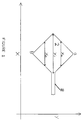
- Figure 1 shows a square, corner fed patch antenna 2, fed by a planar feed 8.
- the maximum value of the X' dimension of the patch is x1 between opposite corners of the antenna.
- the value of the X' dimension decreases through intermediate values x n to zero at the points a and b.
- the length of the patch in the X' direction
- the width in the Y' direction
- FIG. 2 shows an antenna system 1 of the invention.
- An antenna of microstrip construction takes the form of a square planar corner-fed patch 2 mounted on a dielectric layer 3.
- a ground plane 4 clads the underside of the dielectric layer 3.
- a coaxial radio frequency feedthrough 5 has an inner conductor 6 and an outer shield 7.
- the inner conductor 6 is insulated from the dielectric layer 3 and is connected to a planar feed 8 into the corner of the patch antenna 2.
- the outer shield 7 is connected to the ground plane 4.
- a dielectric coupling block 9 is located flush against the patch antenna 2 and the top side of the dielectric layer 3.
- This block 9 is present for radiation purposes and is of PT10, a proprietary material manufactured by Marconi Electronic Devices Ltd., a British company. It is composed of a mixture of alumina and titanium dioxide ceramic materials bound by polystyrene and has a dielectric constant of 10. The thickness of the coupling block approximates to one quarter of the centre frequency of the patch antenna and its overall dimensions are chosen to provide optimum resonance at that frequency.
- a second dielectric block 10 is located flush against the top side of the coupling block 9.
- This second block 10 is present for antireflection purposes and is of polymethylmethacrylate with a dielectric constant of 2.4. It has thickness approximately equal to, but different from, one quarter of the maximum wavelength of the patch antenna.
- the dielectric coupling block 9 is bonded to the dielectric layer 3 and the antireflection block 10 using common household glue.
- dielectric substrate 3 with ground plane 4 and patch antenna 2, dielectric coupling block 9 and dielectric antireflection block 10 are held within an open-ended metal cavity in the form of casing 11.
- the particular mode or modes of resonance set up in dielectric coupling block 9 depends on whether the block 9 is in contact with the metal cavity wall or, as shown here and in figure 3d, there is a gap between the two. It has been found that the best radiation patterns are obtained when a gap of at least 1.5mm is present all round the block 9. Moreover, if a similar gap (not shown) is present between the substrate 3 and the cavity wall then the interaction between the feed line 8 and the metal surround can be minimised.
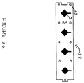
- Figure 3a shows a plan view of an array 12 of four square-planar corner-fed patch antennas 2 on a dielectric substrate 3.
- the underside of the substrate 3 is clad by a copper groundplane (not shown).
- Holes 13 accommodate retaining screws (not shown).
- Figure 3b shows a brass backplate 14 which is assembled flush against (and in electrical contact with) the groundplane of the dielectric substrate 3 shown in figure 3a.
- Holes 13 are tapped to accommodate retaining screws (not shown).
- Holes 15 each accommodate a coaxial feedthrough (not shown).
- the inner conductors of these feedthroughs are insulated from the brass backing plate 14, the dielectric substrate 3 and groundplane, and pass through these to connect with the planar feeds 8 shown in figure 3a.
- the outer shields of the coaxial feedthroughs are connected to the brass backing plate 14.
- Figure 3c shows an aluminium alloy block 11 which is mounted on top of the dielectric substrate shown in figure 2a.
- Four windows 10 are of transparent polymethylmethacrylate and are present for antireflection purposes.
- Sandwiched between each window 10 and the corresponding patch antenna 2 on the dielectric substrate 3 is a dielectric coupling block of PT10 material (not shown).
- the holes 13 accommodate retaining screws (not shown).
- Figure 3d shows a cross section of an assembly of the components of figures 3a, 3b and 3c. Dielectric coupling blocks 9 and their relationship with the other components are shown.
- the plane of the section passes through coaxial feedthroughs 5 with inner conductors 6 and outer shields 7.
- the inner conductors 6 are insulated from, and pass through, the brass backing plate 14 and dielectric substrate 3 and are connected to the planar feeds into the patch antennas (not shown).
- the outer shields 7 are connected to the brass backing plate 14 only.
- Figure 4 shows a dielectric substrate 3 with an array 12 of patch antennas similar to that shown in figure 2a but with the ability to implement orthogonal planes of polarisation. This is achieved by including a second planar feed 8a on each patch antenna. Planar feeds 8 and 8a feed adjacent corners of each patch.
- Figure 5 is a typical linear plot of the match which can be obtained from the type of antenna system described above.
- the vertical axis indicates power which is reflected back along the transmission line rather than being transmitted into free space.
- the diagram shows the variation of this power with signal frequency and a useful bandwidth of about 2 GHz at 20 dB.
- Figure 6 shows typical E-plane and H-plane radiation patterns obtained from this type of antenna system for a signal frequency of 9.6 GHz.
Abstract
Description
- This invention relates to a dielectric resonator antenna system with wide bandwidth and, in particular but not exclusively to, such a system for use as an element in a phased array.
- The dielectric resonator antenna is well known. It may be probe fed (eg S A Long, M W McAllistar and L C Shen; IEEE Transactions on Antennas and Propagation AP-31,
No 3, May 1983, pp406-412 and S A Long and M W McAllistar; International Journal of Infrared and Millimetre Waves, 7, No4, 1986, pp550-570) where the probe has length approximately equal to one quarter of the operating wavelength, and is used to excite a fundamental mode in a coupling block which takes the form of a dielectric puck. The dimensions of the puck are such that it resonates at a specific frequency, this frequency being determined, to a large extent, by the overall volume of the puck. - Alternatively the coupling block may be excited using a patch antenna formed from microstrip, a form of waveguide comprising a copper strip separated from a groundplane by a dielectric substrate. The copper strip is etched to leave an antenna of the required shape and size, typically a square patch fed at the centre of one edge and with the length of each edge equal to half the operating wavelength. Such antennae have the advantage that they occupy little space and can be conveniently connected to form thin planar arrays.
- In an array, each element has its own input and output and by varying the phase of the signal at each element the array can be arranged to transmit or receive in a chosen direction. Moreover the chosen direction can be made time dependant so that a given field can be scanned.
- At the interface between the coupling block and air, some of the signal is reflected rather than transmitted. This loss of power can be minimised by including an antireflection layer between the dielectric layer and the air (eg British Patent Publication no.
GB 2 248 522 A). In order to minimise reflection between two media, the thickness of the antireflection layer should approximate to a quarter wavelength of the signal being transmitted. In addition the material of the antireflection layer should (in theory) have a dielectric constant which approximates to the geometric mean of the dielectric constants of the media on either side. In practice, considerable departure from this ideal is acceptable: for example for matching between air (dielectric constant = 1) and a coupling block of material with dielectric constant = 10, the ideal matching material would have a dielectric constant of 3.16. In practice it is found that polymethylmethacrylate with a dielectric constant of 2.4 serves adequately as a matching material. - Although the foregoing configurations are relatively simple, their use is limited by the inherently narrow range of frequencies over which they can be operated (ie their inherently narrow bandwidth). For example, H LI and C H CHEN describe a probe fed antenna with bandwidth of approximately 200 MHz at 20 dB in Electronics Letters vol. 26 No. 24 (22 November 1990) pp2015-2016. The object of this invention is to provide a dielectric resonator antenna with wide bandwidth.
- According to this invention the bandwidth of a dielectric resonator antenna is greatly enhanced by an appropriate choice of shape for the exciting patch. Specifically it has been shown that if a patch is chosen whose length varies along its width, then a wide range of resonant frequencies can be stimulated therein. Furthermore it has been shown that by employing an antireflection block whose optimum frequency is close to, but slightly different from, the minimum frequency of the patch (typically 5% less), the bandwidth and transmission properties of the device are further improved.
- According to this invention, a dielectric resonating antenna system comprises
- a dielectric substrate sheet having opposing first and second surfaces;
- a patch antenna formed on the first surface, the patch antenna having a length that varies across the width of the patch such that a wide range of resonant frequencies can be stimulated therein;
- a ground plane formed on the second surface;
- means for feeding signals to and, or from the patch antenna and
- a dielectric coupling element adjacent to the first surface whose dielectric constant and dimensions are such that radiation coupling to and from the patch antenna is predominantly through itself.
- In a preferred embodiment, the antenna takes the form of a square. corner-fed patch which is formed on microstrip using the same photo-etching techniques that are standard for making other microwave integrated circuits. An additional advantage of this configuration is that it readily lends itself to implementation of orthogonal planes of polarization by including a second means for feeding signals to and, or from the patch. Other shapes of patch antenna may also provide these properties of enhanced bandwidth and facilitation of orthogonal planes of polarization.
- The preferred means for feeding signals to and, or from the patch antenna is via a coaxial feed through the groundplane and dielectric substrate.
- An additional preferred embodiment includes a dielectric antireflection layer whose dimensions are chosen to provide quarter wavelength antireflection characteristics for an optimum wavelength which is slightly different from the maximum operating wavelength of the patch antenna.
- These components may be enclosed in an open-ended metal cavity which constrains the radiating field to that of an aperture rather than a volume. The dimensions of the cavity may be such that a space (air gap) remains between the coupling element and the cavity wall and/or between the dielectric substrate sheet and the cavity wall.
- Embodiments of the device will now be described, by way of example only, with reference to the accompanying diagrams in which :-
- Figure 1 is an example of the shape of antenna which provides the wide bandwidth properties of the invention.
- Figure 2 is an exploded view of a typical antenna system of the invention in disassembled form.
- Figures 3a, 3b and 3c show the component parts making up a four element sub-array, where each element comprises an antenna system of the invention.
- Figure 3d shows a cross-section of the sub-array assembly. Larger arrays (typically around 2000 elements) are formed by combining a number of sub-arrays such as this.
- Figure 4 shows part of an array of patch antennas of the invention with the implementation of orthogonal planes of polarisation.
- Figure 5 shows the range of frequencies over which a typical antenna system of the invention was found to be useful.
- Figure 6 shows the E-plane and H-plane radiation patterns obtained from a typical antenna system of the invention.
- Figure 1 shows a square, corner fed
patch antenna 2, fed by aplanar feed 8. In this orientation, the maximum value of theX' dimension of the patch is x₁ between opposite corners of the antenna. As the line through which this dimension is taken moves in the Y' direction away from this starting point, the value of theX' dimension decreases through intermediate values xn to zero at the points a and b. Thus the length of the patch (in theX' direction) varies across its width (in theY' direction).
 - Figure 2 shows an antenna system 1 of the invention. An antenna of microstrip construction takes the form of a square planar corner-fed
patch 2 mounted on adielectric layer 3. Aground plane 4 clads the underside of thedielectric layer 3. A coaxialradio frequency feedthrough 5 has aninner conductor 6 and anouter shield 7. Theinner conductor 6 is insulated from thedielectric layer 3 and is connected to aplanar feed 8 into the corner of thepatch antenna 2. Theouter shield 7 is connected to theground plane 4. - A
dielectric coupling block 9 is located flush against thepatch antenna 2 and the top side of thedielectric layer 3. Thisblock 9 is present for radiation purposes and is of PT10, a proprietary material manufactured by Marconi Electronic Devices Ltd., a British company. It is composed of a mixture of alumina and titanium dioxide ceramic materials bound by polystyrene and has a dielectric constant of 10. The thickness of the coupling block approximates to one quarter of the centre frequency of the patch antenna and its overall dimensions are chosen to provide optimum resonance at that frequency. - A second
dielectric block 10 is located flush against the top side of thecoupling block 9. Thissecond block 10 is present for antireflection purposes and is of polymethylmethacrylate with a dielectric constant of 2.4. It has thickness approximately equal to, but different from, one quarter of the maximum wavelength of the patch antenna. - The
dielectric coupling block 9 is bonded to thedielectric layer 3 and theantireflection block 10 using common household glue. - The assembly of the
dielectric substrate 3 withground plane 4 andpatch antenna 2,dielectric coupling block 9 anddielectric antireflection block 10, are held within an open-ended metal cavity in the form ofcasing 11. The particular mode or modes of resonance set up indielectric coupling block 9 depends on whether theblock 9 is in contact with the metal cavity wall or, as shown here and in figure 3d, there is a gap between the two. It has been found that the best radiation patterns are obtained when a gap of at least 1.5mm is present all round theblock 9. Moreover, if a similar gap (not shown) is present between thesubstrate 3 and the cavity wall then the interaction between thefeed line 8 and the metal surround can be minimised. - Figure 3a shows a plan view of an
array 12 of four square-planar corner-fedpatch antennas 2 on adielectric substrate 3. The underside of thesubstrate 3 is clad by a copper groundplane (not shown).Holes 13 accommodate retaining screws (not shown). - Figure 3b shows a
brass backplate 14 which is assembled flush against (and in electrical contact with) the groundplane of thedielectric substrate 3 shown in figure 3a.Holes 13 are tapped to accommodate retaining screws (not shown).Holes 15 each accommodate a coaxial feedthrough (not shown). The inner conductors of these feedthroughs are insulated from thebrass backing plate 14, thedielectric substrate 3 and groundplane, and pass through these to connect with theplanar feeds 8 shown in figure 3a. The outer shields of the coaxial feedthroughs are connected to thebrass backing plate 14. - Figure 3c shows an
aluminium alloy block 11 which is mounted on top of the dielectric substrate shown in figure 2a. Fourwindows 10 are of transparent polymethylmethacrylate and are present for antireflection purposes. Sandwiched between eachwindow 10 and thecorresponding patch antenna 2 on thedielectric substrate 3 is a dielectric coupling block of PT10 material (not shown). Theholes 13 accommodate retaining screws (not shown). - Figure 3d shows a cross section of an assembly of the components of figures 3a, 3b and 3c. Dielectric coupling blocks 9 and their relationship with the other components are shown. The plane of the section passes through
coaxial feedthroughs 5 withinner conductors 6 andouter shields 7. Theinner conductors 6 are insulated from, and pass through, thebrass backing plate 14 anddielectric substrate 3 and are connected to the planar feeds into the patch antennas (not shown). Theouter shields 7 are connected to thebrass backing plate 14 only. - Figure 4 shows a
dielectric substrate 3 with anarray 12 of patch antennas similar to that shown in figure 2a but with the ability to implement orthogonal planes of polarisation. This is achieved by including a second planar feed 8a on each patch antenna. Planar feeds 8 and 8a feed adjacent corners of each patch. - Figure 5 is a typical linear plot of the match which can be obtained from the type of antenna system described above. The vertical axis indicates power which is reflected back along the transmission line rather than being transmitted into free space. The diagram shows the variation of this power with signal frequency and a useful bandwidth of about 2 GHz at 20 dB.
- Figure 6 shows typical E-plane and H-plane radiation patterns obtained from this type of antenna system for a signal frequency of 9.6 GHz.
Claims (9)
- A dielectric resonator antenna system comprising- a dielectric substrate sheet having opposing first and second surfaces;- a patch antenna formed on the first surface, the patch antenna having a length that varies across the width of the patch such that a wide range of resonant frequencies can be stimulated therein;- a ground plane formed on the second surface;- means for feeding signals to and, or from the patch antenna and- a dielectric coupling element adjacent to the first surface whose dielectric constant and dimensions are such that radiation coupling to and from the patch antenna is predominantly through itself.
- The dielectric resonator antenna system of claim 1 where the patch antenna is square and corner fed.
- The dielectric resonator antenna system of claim 1 or 2 with the addition of a second means for feeding signals to and, or from the patch.
- The dielectric resonator antenna system of claims 1, 2 or 3 where the means for feeding signals to and, or from the patch antenna comprises a coaxial cable.
- The dielectric resonator antenna system of any one of the preceding claims with the additional feature of a dielectric matching element whose antireflection characteristics are optimised at a wavelength which is slightly different from the maximum operating wavelength of the patch antenna.
- The dielectric resonator antenna system of any one of the preceding claims where the components are enclosed in an open-ended metal cavity.
- The dielectric resonator antenna system of claim 6 where an air gap is included between the dielectric coupling element and the cavity wall.
- The dielectric antenna system of claim 6 or 7 where an air gap is included between the dielectric substrate and the cavity wall.
- An array of patch antennae elements, each element comprising a dielectric resonator antenna system as claimed in any of the preceding claims.
Applications Claiming Priority (2)
| Application Number | Priority Date | Filing Date | Title |
|---|---|---|---|
| GB9219226 | 1992-09-11 | ||
| GB929219226A GB9219226D0 (en) | 1992-09-11 | 1992-09-11 | Dielectric resonator antenna with wide bandwidth |
Publications (2)
| Publication Number | Publication Date |
|---|---|
| EP0587247A1 true EP0587247A1 (en) | 1994-03-16 |
| EP0587247B1 EP0587247B1 (en) | 2000-01-19 |
Family
ID=10721745
Family Applications (1)
| Application Number | Title | Priority Date | Filing Date |
|---|---|---|---|
| EP19930202597 Expired - Lifetime EP0587247B1 (en) | 1992-09-11 | 1993-09-06 | Dielectric resonator antenna with wide bandwidth |
Country Status (4)
| Country | Link |
|---|---|
| EP (1) | EP0587247B1 (en) |
| DE (1) | DE69327622T2 (en) |
| ES (1) | ES2141126T3 (en) |
| GB (1) | GB9219226D0 (en) |
Cited By (24)
| Publication number | Priority date | Publication date | Assignee | Title |
|---|---|---|---|---|
| EP0755092A2 (en) * | 1995-07-17 | 1997-01-22 | Plessey Semiconductors Limited | Antenna arrangements |
| EP1184933A2 (en) * | 2000-08-10 | 2002-03-06 | Samsung Electronics Co., Ltd. | Resonator |
| EP1271691A2 (en) * | 2001-06-01 | 2003-01-02 | Filtronic LK Oy | Dielectric resonator antenna |
| WO2004109853A1 (en) * | 2003-06-04 | 2004-12-16 | Andrew Fox | Antenna system |
| EP3336575A1 (en) * | 2016-11-18 | 2018-06-20 | Valeo Schalter und Sensoren GmbH | Radar sensor for a motor vehicle with an antenna element embedded in a radome, driver assistance system and motor vehicle |
| WO2018204124A1 (en) * | 2017-05-02 | 2018-11-08 | Rogers Corporation | Electromagnetic reflector for use in a dielectric resonator antenna system |
| CN109616767A (en) * | 2018-11-28 | 2019-04-12 | 哈尔滨工业大学(威海) | A kind of corner-fed dual polarized microstrip patch antenna device of mixing |
| CN109687113A (en) * | 2019-01-22 | 2019-04-26 | 西安电子科技大学 | Filter, dielectric resonant aerial with biradial zero |
| US10355361B2 (en) | 2015-10-28 | 2019-07-16 | Rogers Corporation | Dielectric resonator antenna and method of making the same |
| US10374315B2 (en) | 2015-10-28 | 2019-08-06 | Rogers Corporation | Broadband multiple layer dielectric resonator antenna and method of making the same |
| US10476164B2 (en) | 2015-10-28 | 2019-11-12 | Rogers Corporation | Broadband multiple layer dielectric resonator antenna and method of making the same |
| WO2020055776A1 (en) * | 2018-09-10 | 2020-03-19 | Rogers Corporation | Antenna component with shielded feed |
| US10601137B2 (en) | 2015-10-28 | 2020-03-24 | Rogers Corporation | Broadband multiple layer dielectric resonator antenna and method of making the same |
| US10892544B2 (en) | 2018-01-15 | 2021-01-12 | Rogers Corporation | Dielectric resonator antenna having first and second dielectric portions |
| US10910722B2 (en) | 2018-01-15 | 2021-02-02 | Rogers Corporation | Dielectric resonator antenna having first and second dielectric portions |
| US11031697B2 (en) | 2018-11-29 | 2021-06-08 | Rogers Corporation | Electromagnetic device |
| US11108159B2 (en) | 2017-06-07 | 2021-08-31 | Rogers Corporation | Dielectric resonator antenna system |
| WO2022042817A1 (en) * | 2020-08-24 | 2022-03-03 | Huawei Technologies Co., Ltd. | Mimo antenna array decoupler |
| US11283189B2 (en) | 2017-05-02 | 2022-03-22 | Rogers Corporation | Connected dielectric resonator antenna array and method of making the same |
| US11367959B2 (en) | 2015-10-28 | 2022-06-21 | Rogers Corporation | Broadband multiple layer dielectric resonator antenna and method of making the same |
| US11482790B2 (en) | 2020-04-08 | 2022-10-25 | Rogers Corporation | Dielectric lens and electromagnetic device with same |
| US11552390B2 (en) | 2018-09-11 | 2023-01-10 | Rogers Corporation | Dielectric resonator antenna system |
| US11616302B2 (en) | 2018-01-15 | 2023-03-28 | Rogers Corporation | Dielectric resonator antenna having first and second dielectric portions |
| US11637377B2 (en) | 2018-12-04 | 2023-04-25 | Rogers Corporation | Dielectric electromagnetic structure and method of making the same |
Citations (2)
| Publication number | Priority date | Publication date | Assignee | Title |
|---|---|---|---|---|
| US4191959A (en) * | 1978-07-17 | 1980-03-04 | The United States Of America As Represented By The Secretary Of The Army | Microstrip antenna with circular polarization |
| GB2054275A (en) * | 1979-07-12 | 1981-02-11 | Emi Ltd | Antenna |
-
1992
- 1992-09-11 GB GB929219226A patent/GB9219226D0/en active Pending
-
1993
- 1993-09-06 DE DE1993627622 patent/DE69327622T2/en not_active Expired - Lifetime
- 1993-09-06 EP EP19930202597 patent/EP0587247B1/en not_active Expired - Lifetime
- 1993-09-06 ES ES93202597T patent/ES2141126T3/en not_active Expired - Lifetime
Patent Citations (2)
| Publication number | Priority date | Publication date | Assignee | Title |
|---|---|---|---|---|
| US4191959A (en) * | 1978-07-17 | 1980-03-04 | The United States Of America As Represented By The Secretary Of The Army | Microstrip antenna with circular polarization |
| GB2054275A (en) * | 1979-07-12 | 1981-02-11 | Emi Ltd | Antenna |
Non-Patent Citations (4)
| Title |
|---|
| HAKKAK ET AL.: "GAIN ENHANCEMENT OF DIELECTRIC RESONATOR LOADED WAVEGUIDE ANTENNAS WITH DIELECTRIC OVERLAYS", ELECTRONICS LETTERS., vol. 28, no. 6, 12 March 1992 (1992-03-12), STEVENAGE, GB, pages 541 - 542, XP000287231 * |
| HALL ET AL.: "MICROSTRIP PLANAR ARRAYS WITH DIELECTRIC SPHERE OVERLAYS", WESCON TECHNICAL PAPERS, vol. 28, October 1984 (1984-10-01), NORTH HOLLYWOOD US, pages 356 - 357 * |
| HALL ET JAMES: "Survey of design techniques for flat profile microwave antennas and arrays", RADIO AND ELECTRONIC ENGINEER, vol. 48, no. 11, November 1978 (1978-11-01), LONDON GB, pages 549 - 565 * |
| KRANENBURG ET AL.: "MICROSTRIP TRANSMISSION LINE EXCITATION OF DIELECTRIC RESONATOR ANTENNAS", ELECTRONICS LETTERS., vol. 24, no. 18, 1 September 1988 (1988-09-01), STEVENAGE,GB, pages 1156 - 1157, XP001387857 * |
Cited By (45)
| Publication number | Priority date | Publication date | Assignee | Title |
|---|---|---|---|---|
| EP0755092A3 (en) * | 1995-07-17 | 1999-04-14 | Mitel Semiconductor Limited | Antenna arrangements |
| EP0755092A2 (en) * | 1995-07-17 | 1997-01-22 | Plessey Semiconductors Limited | Antenna arrangements |
| EP1184933A2 (en) * | 2000-08-10 | 2002-03-06 | Samsung Electronics Co., Ltd. | Resonator |
| EP1184933A3 (en) * | 2000-08-10 | 2003-05-14 | Samsung Electronics Co., Ltd. | Resonator |
| US6903692B2 (en) | 2001-06-01 | 2005-06-07 | Filtronic Lk Oy | Dielectric antenna |
| EP1271691A2 (en) * | 2001-06-01 | 2003-01-02 | Filtronic LK Oy | Dielectric resonator antenna |
| EP1271691A3 (en) * | 2001-06-01 | 2003-11-05 | Filtronic LK Oy | Dielectric resonator antenna |
| US7423591B2 (en) | 2003-06-04 | 2008-09-09 | Andrew John Fox | Antenna system |
| WO2004109853A1 (en) * | 2003-06-04 | 2004-12-16 | Andrew Fox | Antenna system |
| GB2420450B (en) * | 2003-06-04 | 2007-12-27 | Andrew Fox | Antenna system |
| GB2420450A (en) * | 2003-06-04 | 2006-05-24 | Andrew Fox | Antenna system |
| US10892556B2 (en) | 2015-10-28 | 2021-01-12 | Rogers Corporation | Broadband multiple layer dielectric resonator antenna |
| US11367960B2 (en) | 2015-10-28 | 2022-06-21 | Rogers Corporation | Dielectric resonator antenna and method of making the same |
| US11367959B2 (en) | 2015-10-28 | 2022-06-21 | Rogers Corporation | Broadband multiple layer dielectric resonator antenna and method of making the same |
| US10601137B2 (en) | 2015-10-28 | 2020-03-24 | Rogers Corporation | Broadband multiple layer dielectric resonator antenna and method of making the same |
| US10355361B2 (en) | 2015-10-28 | 2019-07-16 | Rogers Corporation | Dielectric resonator antenna and method of making the same |
| US10374315B2 (en) | 2015-10-28 | 2019-08-06 | Rogers Corporation | Broadband multiple layer dielectric resonator antenna and method of making the same |
| US10476164B2 (en) | 2015-10-28 | 2019-11-12 | Rogers Corporation | Broadband multiple layer dielectric resonator antenna and method of making the same |
| US10854982B2 (en) | 2015-10-28 | 2020-12-01 | Rogers Corporation | Broadband multiple layer dielectric resonator antenna and method of making the same |
| US10811776B2 (en) | 2015-10-28 | 2020-10-20 | Rogers Corporation | Broadband multiple layer dielectric resonator antenna and method of making the same |
| US10804611B2 (en) | 2015-10-28 | 2020-10-13 | Rogers Corporation | Dielectric resonator antenna and method of making the same |
| US10522917B2 (en) | 2015-10-28 | 2019-12-31 | Rogers Corporation | Broadband multiple layer dielectric resonator antenna and method of making the same |
| US10587039B2 (en) | 2015-10-28 | 2020-03-10 | Rogers Corporation | Broadband multiple layer dielectric resonator antenna and method of making the same |
| EP3336575A1 (en) * | 2016-11-18 | 2018-06-20 | Valeo Schalter und Sensoren GmbH | Radar sensor for a motor vehicle with an antenna element embedded in a radome, driver assistance system and motor vehicle |
| KR20190142318A (en) * | 2017-05-02 | 2019-12-26 | 로저스코포레이션 | Electromagnetic Reflector for Use in Dielectric Resonator Antenna Systems |
| CN110603689A (en) * | 2017-05-02 | 2019-12-20 | 罗杰斯公司 | Electromagnetic reflector for dielectric resonator antenna system |
| GB2573950A (en) * | 2017-05-02 | 2019-11-20 | Rogers Corp | Electromagnetic reflector for use in a dielectric resonator antenna system |
| US11876295B2 (en) | 2017-05-02 | 2024-01-16 | Rogers Corporation | Electromagnetic reflector for use in a dielectric resonator antenna system |
| GB2573950B (en) * | 2017-05-02 | 2022-09-07 | Rogers Corp | Electromagnetic reflector for use in a dielectric resonator antenna system |
| TWI771411B (en) * | 2017-05-02 | 2022-07-21 | 美商羅傑斯公司 | Electromagnetic reflector for use in a dielectric resonator antenna system |
| WO2018204124A1 (en) * | 2017-05-02 | 2018-11-08 | Rogers Corporation | Electromagnetic reflector for use in a dielectric resonator antenna system |
| US11283189B2 (en) | 2017-05-02 | 2022-03-22 | Rogers Corporation | Connected dielectric resonator antenna array and method of making the same |
| US11108159B2 (en) | 2017-06-07 | 2021-08-31 | Rogers Corporation | Dielectric resonator antenna system |
| US10892544B2 (en) | 2018-01-15 | 2021-01-12 | Rogers Corporation | Dielectric resonator antenna having first and second dielectric portions |
| US10910722B2 (en) | 2018-01-15 | 2021-02-02 | Rogers Corporation | Dielectric resonator antenna having first and second dielectric portions |
| US11616302B2 (en) | 2018-01-15 | 2023-03-28 | Rogers Corporation | Dielectric resonator antenna having first and second dielectric portions |
| WO2020055776A1 (en) * | 2018-09-10 | 2020-03-19 | Rogers Corporation | Antenna component with shielded feed |
| US11552390B2 (en) | 2018-09-11 | 2023-01-10 | Rogers Corporation | Dielectric resonator antenna system |
| CN109616767A (en) * | 2018-11-28 | 2019-04-12 | 哈尔滨工业大学(威海) | A kind of corner-fed dual polarized microstrip patch antenna device of mixing |
| CN109616767B (en) * | 2018-11-28 | 2021-04-06 | 哈尔滨工业大学(威海) | Hybrid angle-fed dual-polarization microstrip patch antenna device |
| US11031697B2 (en) | 2018-11-29 | 2021-06-08 | Rogers Corporation | Electromagnetic device |
| US11637377B2 (en) | 2018-12-04 | 2023-04-25 | Rogers Corporation | Dielectric electromagnetic structure and method of making the same |
| CN109687113A (en) * | 2019-01-22 | 2019-04-26 | 西安电子科技大学 | Filter, dielectric resonant aerial with biradial zero |
| US11482790B2 (en) | 2020-04-08 | 2022-10-25 | Rogers Corporation | Dielectric lens and electromagnetic device with same |
| WO2022042817A1 (en) * | 2020-08-24 | 2022-03-03 | Huawei Technologies Co., Ltd. | Mimo antenna array decoupler |
Also Published As
| Publication number | Publication date |
|---|---|
| ES2141126T3 (en) | 2000-03-16 |
| EP0587247B1 (en) | 2000-01-19 |
| DE69327622T2 (en) | 2000-06-08 |
| GB9219226D0 (en) | 1992-10-28 |
| DE69327622D1 (en) | 2000-02-24 |
Similar Documents
| Publication | Publication Date | Title |
|---|---|---|
| US5453754A (en) | Dielectric resonator antenna with wide bandwidth | |
| EP0587247B1 (en) | Dielectric resonator antenna with wide bandwidth | |
| CA2176656C (en) | Broadband circularly polarized dielectric resonator antenna | |
| US5053786A (en) | Broadband directional antenna | |
| Howell | Microstrip antennas | |
| US6285325B1 (en) | Compact wideband microstrip antenna with leaky-wave excitation | |
| EP1082780B1 (en) | Antenna | |
| EP0279050B1 (en) | Three resonator parasitically coupled microstrip antenna array element | |
| US5748153A (en) | Flared conductor-backed coplanar waveguide traveling wave antenna | |
| AU2004302158B2 (en) | Wideband phased array radiator | |
| US5305001A (en) | Horn radiator assembly with stepped septum polarizer | |
| EP0217426A2 (en) | Microstrip antenna device | |
| EP0922312B1 (en) | Planar antenna radiating structure having quasi-scan, frequency-independent driving-point impedance | |
| EP2953207B1 (en) | Circularly-polarized patch antenna | |
| EP2077603A2 (en) | Dielectric leaky wave antenna | |
| GB2268626A (en) | Dielectric resonator antenna. | |
| US5392008A (en) | Orthomode transducer with side-port window | |
| EP0989628B1 (en) | Patch antenna having flexed ground plate | |
| Jagtap et al. | Gain and bandwidth enhancement of circularly polarized MSA using PRS and AMC layers | |
| US4130823A (en) | Miniature, flush mounted, microwave dual band cavity backed slot antenna | |
| Murshed et al. | Designing of a both-sided MIC starfish microstrip array antenna for K-band application | |
| JPH04286204A (en) | Microstrip antenna | |
| Wu et al. | A low-loss unidirectional dielectric radiator (UDR) for antenna and space power combining circuits | |
| US6952184B2 (en) | Circularly polarized antenna having improved axial ratio | |
| EP0598580A1 (en) | Cross-slot microwave antenna |
Legal Events
| Date | Code | Title | Description |
|---|---|---|---|
| PUAI | Public reference made under article 153(3) epc to a published international application that has entered the european phase |
Free format text: ORIGINAL CODE: 0009012 |
|
| AK | Designated contracting states |
Kind code of ref document: A1 Designated state(s): DE ES FR GB IT |
|
| 17P | Request for examination filed |
Effective date: 19941112 |
|
| 17Q | First examination report despatched |
Effective date: 19961220 |
|
| GRAG | Despatch of communication of intention to grant |
Free format text: ORIGINAL CODE: EPIDOS AGRA |
|
| GRAG | Despatch of communication of intention to grant |
Free format text: ORIGINAL CODE: EPIDOS AGRA |
|
| GRAH | Despatch of communication of intention to grant a patent |
Free format text: ORIGINAL CODE: EPIDOS IGRA |
|
| GRAH | Despatch of communication of intention to grant a patent |
Free format text: ORIGINAL CODE: EPIDOS IGRA |
|
| GRAA | (expected) grant |
Free format text: ORIGINAL CODE: 0009210 |
|
| AK | Designated contracting states |
Kind code of ref document: B1 Designated state(s): DE ES FR GB IT |
|
| ITF | It: translation for a ep patent filed |
Owner name: BARZANO' E ZANARDO ROMA S.P.A. |
|
| REF | Corresponds to: |
Ref document number: 69327622 Country of ref document: DE Date of ref document: 20000224 |
|
| ET | Fr: translation filed | ||
| REG | Reference to a national code |
Ref country code: ES Ref legal event code: FG2A Ref document number: 2141126 Country of ref document: ES Kind code of ref document: T3 |
|
| PLBE | No opposition filed within time limit |
Free format text: ORIGINAL CODE: 0009261 |
|
| STAA | Information on the status of an ep patent application or granted ep patent |
Free format text: STATUS: NO OPPOSITION FILED WITHIN TIME LIMIT |
|
| 26N | No opposition filed | ||
| REG | Reference to a national code |
Ref country code: GB Ref legal event code: 732E |
|
| REG | Reference to a national code |
Ref country code: GB Ref legal event code: IF02 |
|
| REG | Reference to a national code |
Ref country code: FR Ref legal event code: TP |
|
| PGFP | Annual fee paid to national office [announced via postgrant information from national office to epo] |
Ref country code: ES Payment date: 20090924 Year of fee payment: 17 |
|
| PGFP | Annual fee paid to national office [announced via postgrant information from national office to epo] |
Ref country code: GB Payment date: 20090922 Year of fee payment: 17 |
|
| PGFP | Annual fee paid to national office [announced via postgrant information from national office to epo] |
Ref country code: DE Payment date: 20090922 Year of fee payment: 17 |
|
| PGFP | Annual fee paid to national office [announced via postgrant information from national office to epo] |
Ref country code: IT Payment date: 20090923 Year of fee payment: 17 |
|
| GBPC | Gb: european patent ceased through non-payment of renewal fee |
Effective date: 20100906 |
|
| PG25 | Lapsed in a contracting state [announced via postgrant information from national office to epo] |
Ref country code: IT Free format text: LAPSE BECAUSE OF NON-PAYMENT OF DUE FEES Effective date: 20100906 |
|
| REG | Reference to a national code |
Ref country code: FR Ref legal event code: ST Effective date: 20110531 |
|
| REG | Reference to a national code |
Ref country code: DE Ref legal event code: R119 Ref document number: 69327622 Country of ref document: DE Effective date: 20110401 |
|
| PG25 | Lapsed in a contracting state [announced via postgrant information from national office to epo] |
Ref country code: DE Free format text: LAPSE BECAUSE OF NON-PAYMENT OF DUE FEES Effective date: 20110401 Ref country code: FR Free format text: LAPSE BECAUSE OF NON-PAYMENT OF DUE FEES Effective date: 20100930 |
|
| PG25 | Lapsed in a contracting state [announced via postgrant information from national office to epo] |
Ref country code: GB Free format text: LAPSE BECAUSE OF NON-PAYMENT OF DUE FEES Effective date: 20100906 |
|
| PGFP | Annual fee paid to national office [announced via postgrant information from national office to epo] |
Ref country code: FR Payment date: 20091001 Year of fee payment: 17 |
|
| REG | Reference to a national code |
Ref country code: ES Ref legal event code: FD2A Effective date: 20111118 |
|
| PG25 | Lapsed in a contracting state [announced via postgrant information from national office to epo] |
Ref country code: ES Free format text: LAPSE BECAUSE OF NON-PAYMENT OF DUE FEES Effective date: 20100907 |