EP0577402A2 - Synchronization signal detector, synchronization signal detecting method and demodulator - Google Patents
Synchronization signal detector, synchronization signal detecting method and demodulator Download PDFInfo
- Publication number
- EP0577402A2 EP0577402A2 EP93305100A EP93305100A EP0577402A2 EP 0577402 A2 EP0577402 A2 EP 0577402A2 EP 93305100 A EP93305100 A EP 93305100A EP 93305100 A EP93305100 A EP 93305100A EP 0577402 A2 EP0577402 A2 EP 0577402A2
- Authority
- EP
- European Patent Office
- Prior art keywords
- bits
- data
- synchronization signal
- signals
- synchronization
- Prior art date
- Legal status (The legal status is an assumption and is not a legal conclusion. Google has not performed a legal analysis and makes no representation as to the accuracy of the status listed.)
- Granted
Links
Images


Classifications
-
- H—ELECTRICITY
- H04—ELECTRIC COMMUNICATION TECHNIQUE
- H04L—TRANSMISSION OF DIGITAL INFORMATION, e.g. TELEGRAPHIC COMMUNICATION
- H04L7/00—Arrangements for synchronising receiver with transmitter
- H04L7/0079—Receiver details
- H04L7/0083—Receiver details taking measures against momentary loss of synchronisation, e.g. inhibiting the synchronisation, using idle words or using redundant clocks
-
- G—PHYSICS
- G11—INFORMATION STORAGE
- G11B—INFORMATION STORAGE BASED ON RELATIVE MOVEMENT BETWEEN RECORD CARRIER AND TRANSDUCER
- G11B20/00—Signal processing not specific to the method of recording or reproducing; Circuits therefor
- G11B20/10—Digital recording or reproducing
- G11B20/14—Digital recording or reproducing using self-clocking codes
- G11B20/1403—Digital recording or reproducing using self-clocking codes characterised by the use of two levels
- G11B20/1423—Code representation depending on subsequent bits, e.g. delay modulation, double density code, Miller code
- G11B20/1426—Code representation depending on subsequent bits, e.g. delay modulation, double density code, Miller code conversion to or from block codes or representations thereof
-
- G—PHYSICS
- G11—INFORMATION STORAGE
- G11B—INFORMATION STORAGE BASED ON RELATIVE MOVEMENT BETWEEN RECORD CARRIER AND TRANSDUCER
- G11B27/00—Editing; Indexing; Addressing; Timing or synchronising; Monitoring; Measuring tape travel
- G11B27/10—Indexing; Addressing; Timing or synchronising; Measuring tape travel
- G11B27/19—Indexing; Addressing; Timing or synchronising; Measuring tape travel by using information detectable on the record carrier
- G11B27/28—Indexing; Addressing; Timing or synchronising; Measuring tape travel by using information detectable on the record carrier by using information signals recorded by the same method as the main recording
- G11B27/30—Indexing; Addressing; Timing or synchronising; Measuring tape travel by using information detectable on the record carrier by using information signals recorded by the same method as the main recording on the same track as the main recording
- G11B27/3027—Indexing; Addressing; Timing or synchronising; Measuring tape travel by using information detectable on the record carrier by using information signals recorded by the same method as the main recording on the same track as the main recording used signal is digitally coded
-
- H—ELECTRICITY
- H04—ELECTRIC COMMUNICATION TECHNIQUE
- H04L—TRANSMISSION OF DIGITAL INFORMATION, e.g. TELEGRAPHIC COMMUNICATION
- H04L7/00—Arrangements for synchronising receiver with transmitter
- H04L7/02—Speed or phase control by the received code signals, the signals containing no special synchronisation information
- H04L7/027—Speed or phase control by the received code signals, the signals containing no special synchronisation information extracting the synchronising or clock signal from the received signal spectrum, e.g. by using a resonant or bandpass circuit
- H04L7/0278—Band edge detection
-
- G—PHYSICS
- G11—INFORMATION STORAGE
- G11B—INFORMATION STORAGE BASED ON RELATIVE MOVEMENT BETWEEN RECORD CARRIER AND TRANSDUCER
- G11B20/00—Signal processing not specific to the method of recording or reproducing; Circuits therefor
- G11B20/10—Digital recording or reproducing
- G11B20/12—Formatting, e.g. arrangement of data block or words on the record carriers
- G11B20/1217—Formatting, e.g. arrangement of data block or words on the record carriers on discs
-
- G—PHYSICS
- G11—INFORMATION STORAGE
- G11B—INFORMATION STORAGE BASED ON RELATIVE MOVEMENT BETWEEN RECORD CARRIER AND TRANSDUCER
- G11B2220/00—Record carriers by type
- G11B2220/20—Disc-shaped record carriers
- G11B2220/25—Disc-shaped record carriers characterised in that the disc is based on a specific recording technology
- G11B2220/2537—Optical discs
- G11B2220/2545—CDs
Definitions
- This invention relates to a synchronization signal detector for detecting synchronization signals (such as frame synchronization signals), a method for detecting the synchronization signals, and a demodulator for demodulating data.
- An eight-to-fourteen modulation (EFM) system is employed in a disc recording system for so-called compact discs (CD), or one of the other disc-shaped recording media, such as optical discs, magnetic discs or magneto-optical discs.
- EFM eight-to-fourteen modulation
- the recording format for a CD is shown in Fig. 12 and in Table 1, in which 24 channel bit synchronization signals (frame synchronization signals), 14 channel bit sub-coding data, 336 (24 x 14) channel bit data and 112 (8 x 14) channel bit parity data are furnished. In addition, 3 bits each are furnished as margin bits for connecting the pattern data, thus totalling 102 channel bits.
- the encoding efficiency and the redundancy of this recording format are 57.1% and 42.9%, respectively.
- the above-mentioned CD recording format is disadvantageous in that: there is only one synchronization signal; margin bits are required for connecting the synchronization signals; and an exceptional bit string is set aside for the synchronization signals.
- each frame of the CD recording format is composed of 588 channel bits, as shown above. If it is assumed that moving picture data is to be recorded on a CD-sized disc, and the recording format is pursuant to the CD recording format and has a frame length longer than that provided in the CD recording format, the distance between the synchronization signals in the frame structure is increased, so that, if the frame structure synchronization is not in order, data restoration tends to be delayed.
- a synchronization signal detector comprising means for extracting edges of RF signals detected as binary-valued signals, means for counting the number of channel clocks produced during a distance between adjacent transitions defined by extracted edges, means for holding the count of the channel clocks generated during a distance between the transitions directly preceding the distance between the transitions for which the number of pulses is currently counted, and means for detecting synchronization signals from outputs of the counting means and said holding means, using two patterns as synchronization signals, one of which is a frame synchronization signal and the other of which is a synchronization signal for at least error correction.
- a demodulating device for demodulating a variable length code comprising a synchronization signal detector section having means for extracting edges of RF signals detected as binary-valued signals, means for counting the number of channel clocks produced during a distance between adjacent transitions defined by extracted edges, means for holding the count of the channel clocks generated during a distance between the transitions directly preceding the distance between the transitions for which the number of pulses is currently counted, and means for detecting synchronization signals from outputs of the counting means and the holding means, using two patterns as synchronization signals, one of which is a frame synchronization signal and the other of which is a synchronization signal for at least error correction.
- the apparatus also comprises a timing controlling section for detecting the block boundary of said variable length code data based on detected synchronization signals, a data demodulating section for demodulating N-bit based variable length code data into M-bit based original data in accordance with a demodulation table performing an inverse conversion to the conversion prescribed by the modulation table used for encoding, based on the detected code length data and output data of the timing control section, and a matching section supplied with the demodulated original data and an output of the timing control section as inputs for matching the original data to an external circuit.
- the synchronization detector of the present embodiment includes a non-return-to-zero inverted (NRZI) circuit 2, as edge detection means, for extracting edges of detected binary-valued RF signals to generate a pulse train, a counter 6 for counting the number of channel clocks T of the distance between transitions which is the distance between the edges extracted from the NRZI circuit 2, that is the number of channel clocks T applied via terminal 4, a latch circuit 5 operated responsive to the pulses from the NRZI circuit 2 to hold the number of channel clocks corresponding to the distance between transitions directly preceding the distance between transitions being counted by counter 6, and AND gates 7 to 12 and an OR gate 13 for detecting synchronization signals from an output of the counter 6 and/or latch circuit 5 using two different patterns as synchronization signals for error correction, with one of the patterns being used as a frame synchronization signal and the other pattern as the synchronization signal for error correction.
- NRZI non-return-to-zero inverted
- the modulation coding employed in the present embodiment is a variable length coding (d, k; m, n; r) having different code word lengths depending on input data word lengths.
- variable length coding is expressed as (d, k; m, n; r) in which d, k means a constraint imposed on a train of the same symbol information, d means the minimum length of a symbol "0", k means the maximum length of the symbol "0", m means the basic data length, n means the basic code length, n/m means a conversion ratio and r means the basic data length of conversion (constraint length).
- 2-7RLL employed in a hard disc is expressed as (2, 7; 1, 2; 4) code.
- (4, 22; 2, 5; 5) code is employed as the (d, k; m, n; r) code.
- a recording format having a frame structure which becomes larger than the frame of the above-described EFM recording format for CD is taken as an example.
- the recording format of the present embodiment employs a block consisting of two frames as a unit for error correction codes, as shown in Fig. 2.
- Fig. 3 shows an overall format.
- the recording format of the present embodiment includes, in the first two frames, 100 channel bit synchronization signals, 640 channel bit sector mark addresses, 2560 channel bit data and 640 channel bit parity data. Also, there are furnished a sum total of 120 channel bits between the patterns as DC control data. Each sector includes 1300 channel bit synchronization signals, 640 channel bit sector mark sector addresses, 40960 channel bit data, 8320 channel bit parity data and 160 channel bit DC control data. The coding efficiency and redundancy of the present format are 7.6% and 22.4%, respectively.
- the synchronization signal (frame synchronization pattern) to use in the case of modulation by the above-mentioned (d, k; m, n; r) code
- the pattern should not appear in the modulated data and preferably the pattern has a minimum length.
- Fig. 4 and Fig. 5 of long bit continuation with the modulation by the (4, 22; 2, 5: 5) are the stream of channel bits of ... for the data strings of ... 0111", “11", “11”, “0111”, “11”, “11”, “0100”, “11", “11”, “0100”, ..., as shown in Fig. 4, and the channel bits of ... for the data strings of ... "0111”, “11”, “11”, “0111”, “11”, “11”, “11”, “0101”, “11”, “11”, “0100”, ..., as shown in Fig. 5.
- Concrete examples of these combinations include a first combination of 22T and 22T (22T - 22T), a second combination of 23T and 21T or 21T and 23T (23T - 21T or 21T - 23T), a third combination of 23T and 22T or 22T and 23T (23T - 22T or 22T - 23T) and a fourth combination of 23t and 23T (23T - 23T).
- pattern string combinations other than the first to fourth combinations may also be contemplated, such as 22T - 21T - 21T combination, However, this leads to increased redundancy. For this reason, the data string combinations with the least possible number of bits are employed in the present embodiment.
- the frame synchronization patterns employed in the present embodiment are characterized in that the patterns can be formed by a bit length ("0" continuation) which is less than the maximum distance between transitions of magnetization Tmax (first combination of 22T - 22T), in that they can be formed by a combination of different bit lengths inclusive of a bit length equal to the maximum distance between transitions of magnetization Tmax (the second combination of 23T and 21T or 21T and 23T or the third combination of 23T and 22T or 22T and 23T) and in that they can be formed by a combination of two contiguous maximum distances between transitions of magnetization Tmax (fourth combination of 23T and 23T).
- the combination of 23T, 21T and 6T is used as the synchronization signal A, while the combination of 21T, 23T and 6T is used as the synchronization signal B.
- the 6T of the synchronization signals A and B are the bits appended for tail adjustment for providing a bit length equal to multiples of 5.
- the frame length is longer than that with the above-mentioned CD recording format. For this reason, the parity data for error correction code is increased in volume and in need of 32 bytes in terms of data bits.
- a frame is desirably of a shorter length.
- the synchronization signals A and B are employed in the present embodiment in such a manner that the unit of parity appended for error correction coding (data and sector mark 16 x 10 bytes plus 32 parity bytes) may be in the form of 2 frames (with each frame being 16 x 5 bytes + 16 bytes). That is, the synchronization signal A is used for frame synchronization and synchronization of ECC parity data, while the synchronization signal B is used exclusively for frame synchronization.
- the frame synchronization signal may be set so as to be arbitrarily shorter than the length of a block to which error correction code data is appended, as a result of which the error correction code data construction may be increased in the number of the degrees of freedom without being limited by the frame length.
- the synchronization signal detector of the present embodiment is a synchronization signal detector capable of detecting the above-mentioned synchronization signals A and B.
- binary-valued signals which are RF signals, produced by an optical pickup or a magnetic head reading signal recording regions or pits recorded on a recording medium, such as an optical disc, magnetic disc or a magneto-optical disc, in accordance with the above-depicted recording format of the present embodiment, and clipped at a constant level as a threshold level, are transmitted to an input terminal 1.
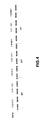
- binary-valued RF signals are supplied to the NRZI circuit 2 which is operated based on channel clocks from terminal 4 for producing a pulse train based on extracted edge portions of the binary-valued signals. If the binary-valued RF signals are taken as so-called non-return-to-zero (NRZ) signals, having their state inverted at the boundary of the bit information, a pulse train formed by extracted edge portions may be produced by the NRZI circuit 2 inverting the signal state only when the bit information has a value of "1", as shown in Fig. 6.
- NRZ non-return-to-zero
- the data supplied to the input terminal 1 is the NRZ data, where "1” and “0” stands for “H” and “L”, respectively the data is converted into NRZI data by the NRZI circuit 2, where "1” means inversion and "0” means non-inversion.
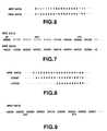
- the NRZ data is a data string consisting of 5T, 23T and 17T, as shown in Fig. 7, the NRZ data is converted into NRZI data in such a manner that data "1" is present at the point of transition from “0” to “1” or from “1” to “0".
- the pulse train from the NRZI circuit 2 is supplied to a clear terminal of the counter 6 and to a load terminal of a latch circuit 5.
- the channel clocks from terminal 4 are supplied to clock terminals of the counter 6 and the latch circuit 5.
- the counter 6 has a count capacity of counting the number of the longest channel clocks of the transition patterns of the synchronization signals to be detected, and counts the number of the channel clocks T between the edges, that is the number of channel clocks between the edges (transition distances) extracted by the NRZI circuit 2.
- the latch circuit 5 holds the count value of the counter 6 (number of channel clocks) and transmits the value of the channel clocks (count value) held thereby to the next stage each time transition of the binary-valued RF signals is incurred, that is each time an edge extracted by the NRZI circuit 2 is encountered.
- the latch circuit 5 holds the value of the number of channel clocks (count value) corresponding to the distance between transitions directly preceding the distance between transitions being counted by the counter 6 and transmits the thus held count value to the next stage.
- the counter 6 and the latch circuit 5 are arranged in a 5-bit output configuration. That is, the output terminals of the counter 6 and the latch circuit 5 are connected to respective input terminals of AND gates 7 to 10.
- the output terminals of the counter 6 associated with first, second and fourth of the 0th to fourth bits of the five-bit output of the counter 6 are connected to the three input terminals of the AND gate 10, while the output terminals of the counter associated with the second and fourth bits are connected to the two input terminals of the AND gate 9.
- the output terminals of the latch circuit 5 associated with first, second and fourth of the 0th to fourth bits of the five-bit output of the latch circuit 5 are connected to three input terminals of the AND gate 7, while the output terminals of the latch circuit 5 associated with the second and fourth bits are connected to the two input terminals of the AND gate 8.
- the outputs of the AND gates 8 and 10 are supplied to two input terminals of a three-input AND gate 11, while the outputs of the AND gates 7 and 9 are supplied to two input terminals of a three-input AND gate 12.
- Outputs of the NRZI circuit 2 are supplied to the remaining input terminals of the AND gates 11 and 12.
- the NRZI data from the NRZI circuit 2 are used as timing signals in the AND gates 11 and 12.
- the AND gates 7 to 10 detect 21T or 23T.
- the AND gates 11, 12 detect the synchronization signal when the combination of 21T and 23T or the combination of 23T and 21T is encountered and "1" is entered from NRZI circuit 2.
- Outputs of the AND gates 11, 12 are transmitted to associated input terminals of the two-input OR gate 13.
- An ORed output of the OR gate 13 is output at output terminal 14 as a synchronization signal detection output of the present detector.
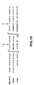
- the synchronization pattern consisting of the combination of 23T and 21T in the NRZI representation is detected as shown in Fig. 9.
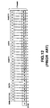
- the NRZI data becomes "1" at a timing ta so that counter 6 is cleared to "0".
- the latch circuit 5 holds the directly previous count value by fetching the previous count value "22".
- the synchronization signal is detected. That is, the count value becomes 20, while the latch circuit 5 holds the count value of "22" at a timing directly preceding timing tb .
- This count value thus held by latch circuit 5, becomes the synchronization signal. If "1" appears in data at the timing tb , the synchronization signal is detected by the AND gates 7 to 12 and the OR gate 13.
- a 1-clock synchronization signal detection output is issued when the above data corresponding to the synchronization signal is entered.
- the synchronization pattern is a 23T - 21T combination
- data is NRZI representation including 22 contiguous "0"s and 20 contiguous "0”s is detected.
- the synchronization pattern is a 21T - 23T combination
- data in NRZI representation including 20 contiguous "0"s and 22 contiguous "0”s is detected.
- the demodulating device is a decoding device for decoding the above-mentioned variable length coded data and includes, as shown in Fig. 11, a synchronization signal detection circuit 22, arranged as shown in Fig. 1, a timing supervising circuit 23 for detecting the boundary between the blocks of the variable length coded data, based on the synchronization signals detected by the synchronization signal detector 22, and a code length detection circuit 24 for detecting the code length of the variable length coded data.
- the demodulating device also includes a data demodulating circuit 25 for demodulating the N-bit based variable length coded data into M-bit based original data in accordance with a demodulating table as a counterpart of the modulating table employed for variable length encoding based on the code length data detected by the code length detection circuit 24 and output data of the timing supervising circuit 23.
- the demodulating device includes an external interface 26 to which the original data demodulated by the data demodulating circuit 25 and an output of the timing supervising circuit 23 are entered and which effectuates matching between the original data-and the downstream side circuit.
- synchronization signals are detected by the synchronization signal detector 22 from data supplied thereto.
- the timing control circuit 23 Based on the synchronization signals, detected by detector 22, the timing control circuit 23 generates timing signals employed for timing control during data demodulation.
- the code length is detected by the code length detection circuit 24.
- the data demodulating circuit 25 demodulates data supplied to input terminal 21.
- Demodulated data from data demodulating circuit 25 are transmitted to the external interface 26 which effectuates matching with the downstream side circuit based on the timing signals.
- the external circuit 26 translates the 10-bit data from the data demodulating circuit 25 into 8-bit data to output the resulting data.
- An output of the external interface 26 is output at output terminal 27 as demodulated data.
- variable length codes of the present embodiment are employed in a format employed for recording moving picture data on e.g. a compact disc (CD).
- CD compact disc
Landscapes
- Engineering & Computer Science (AREA)
- Signal Processing (AREA)
- Computer Networks & Wireless Communication (AREA)
- Signal Processing For Digital Recording And Reproducing (AREA)
- Compression, Expansion, Code Conversion, And Decoders (AREA)
- Synchronisation In Digital Transmission Systems (AREA)
Abstract
Description
- This invention relates to a synchronization signal detector for detecting synchronization signals (such as frame synchronization signals), a method for detecting the synchronization signals, and a demodulator for demodulating data.
- An eight-to-fourteen modulation (EFM) system is employed in a disc recording system for so-called compact discs (CD), or one of the other disc-shaped recording media, such as optical discs, magnetic discs or magneto-optical discs. With this modulation system, data are processed on the basis of units or strings of 8 bits, and each 8-bit bit string is translated into a string of 14-channel bits.
- The recording format for a CD is shown in Fig. 12 and in Table 1, in which 24 channel bit synchronization signals (frame synchronization signals), 14 channel bit sub-coding data, 336 (24 x 14) channel bit data and 112 (8 x 14) channel bit parity data are furnished. In addition, 3 bits each are furnished as margin bits for connecting the pattern data, thus totalling 102 channel bits. One of the roles of the margin bits is to adjust the maximum distance between transitions of magnetization Tmax = 11 T in order not to be repeated twice for the synchronization signals. The encoding efficiency and the redundancy of this recording format are 57.1% and 42.9%, respectively.
TABLE 1 data channel bit sync signals - 24 subcoding 8 14 data 192 336 parity 64 112 margin bits - 102 total 264 588 - The above-mentioned CD recording format is disadvantageous in that: there is only one synchronization signal; margin bits are required for connecting the synchronization signals; and an exceptional bit string is set aside for the synchronization signals.
- Meanwhile, each frame of the CD recording format is composed of 588 channel bits, as shown above. If it is assumed that moving picture data is to be recorded on a CD-sized disc, and the recording format is pursuant to the CD recording format and has a frame length longer than that provided in the CD recording format, the distance between the synchronization signals in the frame structure is increased, so that, if the frame structure synchronization is not in order, data restoration tends to be delayed.
- In accordance with the present invention, there is provided a synchronization signal detector comprising means for extracting edges of RF signals detected as binary-valued signals, means for counting the number of channel clocks produced during a distance between adjacent transitions defined by extracted edges, means for holding the count of the channel clocks generated during a distance between the transitions directly preceding the distance between the transitions for which the number of pulses is currently counted, and means for detecting synchronization signals from outputs of the counting means and said holding means, using two patterns as synchronization signals, one of which is a frame synchronization signal and the other of which is a synchronization signal for at least error correction.
- In accordance with the present invention, there is also provided a demodulating device for demodulating a variable length code comprising a synchronization signal detector section having means for extracting edges of RF signals detected as binary-valued signals, means for counting the number of channel clocks produced during a distance between adjacent transitions defined by extracted edges, means for holding the count of the channel clocks generated during a distance between the transitions directly preceding the distance between the transitions for which the number of pulses is currently counted, and means for detecting synchronization signals from outputs of the counting means and the holding means, using two patterns as synchronization signals, one of which is a frame synchronization signal and the other of which is a synchronization signal for at least error correction. The apparatus also comprises a timing controlling section for detecting the block boundary of said variable length code data based on detected synchronization signals, a data demodulating section for demodulating N-bit based variable length code data into M-bit based original data in accordance with a demodulation table performing an inverse conversion to the conversion prescribed by the modulation table used for encoding, based on the detected code length data and output data of the timing control section, and a matching section supplied with the demodulated original data and an output of the timing control section as inputs for matching the original data to an external circuit.
- Further respective aspects of the invention are set forth in the claims.
- The invention will now be described by way of example with reference to the accompanying drawings, throughout which like parts are referred to by like references, and in which:
- Fig. 1 is a schematic block circuit diagram showing a synchronization signal detector according to an embodiment of the present invention;
- Fig. 2 illustrates a frame structure and the unit of an error correction coding;
- Fig. 3 illustrates an entire recording format;
- Fig. 4 illustrates an example of synchronization signals;
- Fig. 5 illustrates another example of synchronization signals;
- Fig. 6 illustrates conversion of NRZ data into NRZI data;
- Fig. 7 illustrates conversion of the synchronization signals into NRZI data;
- Fig. 8 illustrates the operation of a counter and a latch circuit of the synchronization signal detector;
- Fig. 9 illustrates a synchronization pattern in NRZI representation;
- Fig. 10 illustrates the operation of the counter and the latch circuit at the time of detection of synchronization signals;
- Fig. 11 is a schematic block circuit diagram showing a decoder; and
- Fig. 12 illustrates a CD recording format.
- Referring to the drawings, preferred embodiments of the synchronization detector, method for detecting synchronization signals and the decoder relevant to the synchronization detector are explained in detail.
- Referring to Fig. 1, the synchronization detector of the present embodiment includes a non-return-to-zero inverted (NRZI)
circuit 2, as edge detection means, for extracting edges of detected binary-valued RF signals to generate a pulse train, acounter 6 for counting the number of channel clocks T of the distance between transitions which is the distance between the edges extracted from theNRZI circuit 2, that is the number of channel clocks T applied viaterminal 4, alatch circuit 5 operated responsive to the pulses from theNRZI circuit 2 to hold the number of channel clocks corresponding to the distance between transitions directly preceding the distance between transitions being counted bycounter 6, and ANDgates 7 to 12 and anOR gate 13 for detecting synchronization signals from an output of thecounter 6 and/orlatch circuit 5 using two different patterns as synchronization signals for error correction, with one of the patterns being used as a frame synchronization signal and the other pattern as the synchronization signal for error correction. - The modulation coding employed in the present embodiment is a variable length coding (d, k; m, n; r) having different code word lengths depending on input data word lengths. Before proceeding to the description of the arrangement shown in Fig. 1, the variable length coding is explained.
- The variable length coding is expressed as (d, k; m, n; r) in which d, k means a constraint imposed on a train of the same symbol information, d means the minimum length of a symbol "0", k means the maximum length of the symbol "0", m means the basic data length, n means the basic code length, n/m means a conversion ratio and r means the basic data length of conversion (constraint length). For example, the so-called 2-7RLL employed in a hard disc is expressed as (2, 7; 1, 2; 4) code.
- In the present embodiment, (4, 22; 2, 5; 5) code is employed as the (d, k; m, n; r) code.
- The data and the conversion table with the (4, 22; 2, 5; 5) code is shown in Table 2.


- In the present embodiment described herein, a recording format having a frame structure which becomes larger than the frame of the above-described EFM recording format for CD is taken as an example. The recording format of the present embodiment employs a block consisting of two frames as a unit for error correction codes, as shown in Fig. 2. Table 4 shows an arrangement of a sector (= 26 frames) and Fig. 3 shows an overall format.
TABLE 3 data channel bit sync signals - 100 sector mark/sector address 256 640 data 1024 2560 parity 256 640 DC control - 120 TABLE 4 data channel bit sync signals - 1300 sector mark/sector address 256 640 data 16384 40960 parity 3328 8320 DC control - 1560 total 19968 52780 - Referring to Table 3 and Fig. 2, the recording format of the present embodiment includes, in the first two frames, 100 channel bit synchronization signals, 640 channel bit sector mark addresses, 2560 channel bit data and 640 channel bit parity data. Also, there are furnished a sum total of 120 channel bits between the patterns as DC control data. Each sector includes 1300 channel bit synchronization signals, 640 channel bit sector mark sector addresses, 40960 channel bit data, 8320 channel bit parity data and 160 channel bit DC control data. The coding efficiency and redundancy of the present format are 7.6% and 22.4%, respectively.
- According to Table 2, it can be seen that consecutive data strings translate to channel bits. These channel bits, under this code, are sets of contiguous "0" channel bits separated by a single "1" channel bit, where each "1" channel bit represents a transition of magnetization. By placing various data strings together, it can be seen that there is a maximum distance between transitions of magnetization (Tmax) and a minimum distance between transitions of magnetization (Tmin). Under modulation by the above-mentioned (4, 22; 2, 5; 5) code, Tmax = 32 and Tmin = 5.
- For the synchronization signal (frame synchronization pattern) to use in the case of modulation by the above-mentioned (d, k; m, n; r) code, it is necessary to select a pattern in which the maximum distance between transitions of magnetization Tmax is not increased, and the minimum distance between transitions of magnetization Tmin is not excessively decreased. Also, the pattern should not appear in the modulated data and preferably the pattern has a minimum length.
- With the present embodiment, possible examples of long bit lengths (lengths of contiguous "0" bits) appearing in data, with the modulation by above-mentioned (d, k; m, n; r) code as the frame synchronization pattern, are those shown in Figs.4 and 5.
- The examples of Fig. 4 and Fig. 5 of long bit continuation with the modulation by the (4, 22; 2, 5: 5) are the stream of channel bits of ...

for the data strings of ... 0111", "11", "11", "0111", "11", "11", "0100", "11", "11", "0100", ..., as shown in Fig. 4, and the channel bits of ...
for the data strings of ... "0111", "11", "11", "0111", "11", "11", "0101", "11", "11", "0100", ..., as shown in Fig. 5. - It is seen from Fig. 4 that, should there appear 23 T, that is 22 contiguous "0" channel bits, the bit lengths before and after it are both 20T, which represents the maximum value, 19, of contiguous "0" channel bits that can appear before or after a 23T. It is also seen from Fig. 5 that, should there appear 22 T, that is 21 contiguous "0" channel bits, the bit lengths before and after it cannot exceed 21T, which represents up to a maximum value of 20 contiguous "0" channel bits.
- It is seen from this that, among contiguous pattern strings each having a bit length not exceeding 23 T, where T denotes the distance between bits (channel clocks), that is a bit length not exceeding the maximum distance between transitions of magnetization Tmax = 23T, there are certain combinations of contiguous pattern strings which do not appear in the modulation by the above-mentioned (4, 22; 2, 5; 5) code.
- Concrete examples of these combinations include a first combination of 22T and 22T (22T - 22T), a second combination of 23T and 21T or 21T and 23T (23T - 21T or 21T - 23T), a third combination of 23T and 22T or 22T and 23T (23T - 22T or 22T - 23T) and a fourth combination of 23t and 23T (23T - 23T).
- If the number of bits is increased, pattern string combinations other than the first to fourth combinations may also be contemplated, such as 22T - 21T - 21T combination, However, this leads to increased redundancy. For this reason, the data string combinations with the least possible number of bits are employed in the present embodiment.
- It is mandatory, in this embodiment, that patterns which never appear in data be used as the frame synchronization signals (synchronization signals). With the present embodiment, this is taken into account when selecting the patterns of the frame synchronization signals among the above-mentioned first combination through fourth combination.
- The frame synchronization patterns employed in the present embodiment are characterized in that the patterns can be formed by a bit length ("0" continuation) which is less than the maximum distance between transitions of magnetization Tmax (first combination of 22T - 22T), in that they can be formed by a combination of different bit lengths inclusive of a bit length equal to the maximum distance between transitions of magnetization Tmax (the second combination of 23T and 21T or 21T and 23T or the third combination of 23T and 22T or 22T and 23T) and in that they can be formed by a combination of two contiguous maximum distances between transitions of magnetization Tmax (fourth combination of 23T and 23T).
- Since the present embodiment has no margin bit, such as that provided in the aforementioned CD format, the maximum distance between transitions of magnetization Tmax = 23T and the minimum distance between transitions of magnetization Tmin = 5T need to be satisfied solely by synchronization signals. Also, since the (4, 22; 2, 5: 5) code is a variable length type recording code based on the 2/5 modulation, it is desirable from hardware configuration considerations that the bit length be equal to multiples of 5.
- From the foregoing consideration, the following two synchronization signals have been selected for the present embodiment.
- That is, the combination of 23T, 21T and 6T is used as the synchronization signal A, while the combination of 21T, 23T and 6T is used as the synchronization signal B. The 6T of the synchronization signals A and B are the bits appended for tail adjustment for providing a bit length equal to multiples of 5.
- As described above, with the recording format of the present embodiment, the frame length is longer than that with the above-mentioned CD recording format. For this reason, the parity data for error correction code is increased in volume and in need of 32 bytes in terms of data bits.
- Consequently, if, with the recording format of the present embodiment, failure in synchronization is incurred due to readout errors, data demodulation cannot be achieved until detection of the next synchronization signals. With a larger frame length, the volume of lost data is also increased. For this reason, a frame is desirably of a shorter length.
- In this consideration, the synchronization signals A and B are employed in the present embodiment in such a manner that the unit of parity appended for error correction coding (data and sector mark 16 x 10 bytes plus 32 parity bytes) may be in the form of 2 frames (with each frame being 16 x 5 bytes + 16 bytes). That is, the synchronization signal A is used for frame synchronization and synchronization of ECC parity data, while the synchronization signal B is used exclusively for frame synchronization.
- By using plural synchronization signals, it becomes possible for the respective synchronization signals to take charge of different functions. In this manner, the frame synchronization signal may be set so as to be arbitrarily shorter than the length of a block to which error correction code data is appended, as a result of which the error correction code data construction may be increased in the number of the degrees of freedom without being limited by the frame length.
- The synchronization signal detector of the present embodiment is a synchronization signal detector capable of detecting the above-mentioned synchronization signals A and B.
- Returning to Fig. 1, showing the synchronization signal detector of the present embodiment, binary-valued signals, which are RF signals, produced by an optical pickup or a magnetic head reading signal recording regions or pits recorded on a recording medium, such as an optical disc, magnetic disc or a magneto-optical disc, in accordance with the above-depicted recording format of the present embodiment, and clipped at a constant level as a threshold level, are transmitted to an
input terminal 1. - These binary-valued RF signals are supplied to the
NRZI circuit 2 which is operated based on channel clocks fromterminal 4 for producing a pulse train based on extracted edge portions of the binary-valued signals. If the binary-valued RF signals are taken as so-called non-return-to-zero (NRZ) signals, having their state inverted at the boundary of the bit information, a pulse train formed by extracted edge portions may be produced by theNRZI circuit 2 inverting the signal state only when the bit information has a value of "1", as shown in Fig. 6. - In other words, if the data supplied to the
input terminal 1 is the NRZ data, where "1" and "0" stands for "H" and "L", respectively the data is converted into NRZI data by theNRZI circuit 2, where "1" means inversion and "0" means non-inversion. For example, if the NRZ data is a data string consisting of 5T, 23T and 17T, as shown in Fig. 7, the NRZ data is converted into NRZI data in such a manner that data "1" is present at the point of transition from "0" to "1" or from "1" to "0". In the example of Fig. 7, by conversion of the NRZ data into NRZI data, four "0"s are arrayed during 5T, 22 "0"s are arrayed during 23T and 16 "0"s are arrayed during 17T. Consequently, the aforementioned synchronization signal pattern has 22 "0"s followed by one "1" followed in turn by 20 "0"s, as shown in Fig. 9, or alternatively, 20 "0"s followed by one "1" followed in turn by 22 "0"s. - The pulse train from the
NRZI circuit 2 is supplied to a clear terminal of thecounter 6 and to a load terminal of alatch circuit 5. The channel clocks fromterminal 4 are supplied to clock terminals of thecounter 6 and thelatch circuit 5. - The
counter 6 has a count capacity of counting the number of the longest channel clocks of the transition patterns of the synchronization signals to be detected, and counts the number of the channel clocks T between the edges, that is the number of channel clocks between the edges (transition distances) extracted by theNRZI circuit 2. - The
latch circuit 5 holds the count value of the counter 6 (number of channel clocks) and transmits the value of the channel clocks (count value) held thereby to the next stage each time transition of the binary-valued RF signals is incurred, that is each time an edge extracted by theNRZI circuit 2 is encountered. In other words, thelatch circuit 5 holds the value of the number of channel clocks (count value) corresponding to the distance between transitions directly preceding the distance between transitions being counted by thecounter 6 and transmits the thus held count value to the next stage. - That is, since "1" stands for a point of run interruption, counter 6 counts up by +1 each time "0" data is encountered, while
latch circuit 5 holds the count value from thecounter 6. Conversely, if the data is "1",counter 6 is cleared, while thelatch circuit 5 loads the count value fromcounter 5, that is the current count value. - The
counter 6 and thelatch circuit 5 are arranged in a 5-bit output configuration. That is, the output terminals of thecounter 6 and thelatch circuit 5 are connected to respective input terminals of ANDgates 7 to 10. - Specifically, the output terminals of the
counter 6 associated with first, second and fourth of the 0th to fourth bits of the five-bit output of thecounter 6 are connected to the three input terminals of the ANDgate 10, while the output terminals of the counter associated with the second and fourth bits are connected to the two input terminals of the ANDgate 9. Also, the output terminals of thelatch circuit 5 associated with first, second and fourth of the 0th to fourth bits of the five-bit output of thelatch circuit 5 are connected to three input terminals of the ANDgate 7, while the output terminals of thelatch circuit 5 associated with the second and fourth bits are connected to the two input terminals of the ANDgate 8. - The outputs of the AND
gates gate 11, while the outputs of the ANDgates gate 12. Outputs of theNRZI circuit 2 are supplied to the remaining input terminals of the ANDgates NRZI circuit 2 are used as timing signals in the ANDgates - With the present embodiment, the AND
gates 7 to 10 detect 21T or 23T. On the other hand, the ANDgates NRZI circuit 2. - Outputs of the AND
gates gate 13. An ORed output of theOR gate 13 is output atoutput terminal 14 as a synchronization signal detection output of the present detector. - Specifically, the synchronization pattern consisting of the combination of 23T and 21T in the NRZI representation is detected as shown in Fig. 9.
- Referring to Fig. 10, the NRZI data becomes "1" at a timing ta so that
counter 6 is cleared to "0". Thelatch circuit 5 holds the directly previous count value by fetching the previous count value "22". At a timing tb, the synchronization signal is detected. That is, the count value becomes 20, while thelatch circuit 5 holds the count value of "22" at a timing directly preceding timing tb. This count value, thus held bylatch circuit 5, becomes the synchronization signal. If "1" appears in data at the timing tb, the synchronization signal is detected by the ANDgates 7 to 12 and theOR gate 13. - It is seen from above that a 1-clock synchronization signal detection output is issued when the above data corresponding to the synchronization signal is entered. For example, when the synchronization pattern is a 23T - 21T combination, data is NRZI representation including 22 contiguous "0"s and 20 contiguous "0"s is detected. Similarly, when the synchronization pattern is a 21T - 23T combination, data in NRZI representation including 20 contiguous "0"s and 22 contiguous "0"s is detected.
- The demodulating device of the present embodiment is now explained.
- The demodulating device is a decoding device for decoding the above-mentioned variable length coded data and includes, as shown in Fig. 11, a synchronization
signal detection circuit 22, arranged as shown in Fig. 1, atiming supervising circuit 23 for detecting the boundary between the blocks of the variable length coded data, based on the synchronization signals detected by thesynchronization signal detector 22, and a codelength detection circuit 24 for detecting the code length of the variable length coded data. The demodulating device also includes adata demodulating circuit 25 for demodulating the N-bit based variable length coded data into M-bit based original data in accordance with a demodulating table as a counterpart of the modulating table employed for variable length encoding based on the code length data detected by the codelength detection circuit 24 and output data of thetiming supervising circuit 23. Finally, the demodulating device includes anexternal interface 26 to which the original data demodulated by thedata demodulating circuit 25 and an output of thetiming supervising circuit 23 are entered and which effectuates matching between the original data-and the downstream side circuit. - Referring to Fig. 11, data read out from a recording medium, such as an optical disc, are supplied to an
input terminal 21. The above-mentioned synchronization signals are detected by thesynchronization signal detector 22 from data supplied thereto. Based on the synchronization signals, detected bydetector 22, thetiming control circuit 23 generates timing signals employed for timing control during data demodulation. - Since it is necessary with the variable length coding to detect code length for data demodulation, the code length is detected by the code
length detection circuit 24. - Using the code length data from the code
length detection circuit 24 and the timing signals from thetiming control circuit 23, thedata demodulating circuit 25 demodulates data supplied to input terminal 21. Demodulated data fromdata demodulating circuit 25 are transmitted to theexternal interface 26 which effectuates matching with the downstream side circuit based on the timing signals. By way of an example, theexternal circuit 26 translates the 10-bit data from thedata demodulating circuit 25 into 8-bit data to output the resulting data. An output of theexternal interface 26 is output atoutput terminal 27 as demodulated data. - It is noted that the variable length codes of the present embodiment are employed in a format employed for recording moving picture data on e.g. a compact disc (CD).
- Although the present invention has been shown and described with respect to preferred embodiments, various changes and modifications which are obvious to a person skilled in the art to which the invention pertains are deemed to lie within the scope of the invention as claimed.
Claims (14)
- A synchronization signal detector for detecting synchronization signals embedded in radio frequency (RF) signals containing data encoded according to a modulation table, the synchronization signal detector comprising:
means (2) for extracting edges of the RF signals detected as binary-valued signals,
counting means (6) for counting a number of channel clocks generated by an external channel clock generator between adjacent extracted edges,
holding means (5) for holding a count of the channel clocks previously counted by the counting means while the counting means counts a current number of channel clocks generated between adjacent extracted edges, and
means (7,8,9,10,11,12,13) for receiving outputs of the counting means (6) and the holding means (5) and for detecting synchronization signals by comparing the outputs of the counting means (6) and the holding means (5) with synchronization signals comprising two patterns, one pattern representing a frame synchronization signal and the other pattern representing a synchronization signal for at least error correction. - A synchronization signal detector as claimed in claim 1, wherein each of the two patterns comprises a combination of bit counts not present in the encoded data, bit lengths representing clocks counted between extracted edges in the synchronization signals, each bit count being less than or equal to Tmax, which is the maximum number of clocks between extracted edges in the coded data, and greater than or equal to Tmin, which is the minimum number of clocks between extracted edges in the coded data, inclusive, the patterns also satisfying at least one of the following conditions (i) to (iii):(i) the patterns are each a combination of bit lengths smaller than a maximum number of bit counts between transitions of magnetization of the conversion code;(ii) the patterns are each a combination of different bit counts inclusive of Tmax; and(iii) the patterns are each a combination of Tmax and another Tmax contiguous thereto.
- A synchronization signal detector as claimed in claim 1, wherein a modulation code used for encoding the encoded data is a variable length code having different code word lengths depending on input data word lengths, the variable length code being in the format of (d, k; m, n; r), where d, k means a constraint imposed on a train of the same symbol information (d means a minimum length of a symbol "0", k means a maximum length of the symbol "0"), m means a basic data length, n means a basic code length, and r means a basic data length of conversion (constraint length), and d, k, m, n, r, Tmax and Tmin have the following values:
d = 4;
k = 22;
m = 2;
n = 5;
r = 5;
Tmax = 23T and
Tmin = 5T. - A synchronization signal detector as claimed in claim 3, wherein a spacing between transitions in each of the two patterns comprises one of the following: 22 bits followed by 22 bits, 23 bits followed by 21 bits, 21 bits followed by 23 bits, 23 bits followed by 22 bits, 22 bits followed by 23 bits, and 23 bits followed by 23 bits.
- A synchronization signal detector as claimed in claim 1, wherein a margin bit for tail adjustment is appended to each pattern.
- A synchronization signal detector as claimed in claim 5, wherein a total number of bits of the pattern of each of the synchronization signals, including the appended margin bit, is equal to a multiple of five.
- A demodulating device for demodulating variable length code data comprising:
a synchronization signal detector (22) comprising means (2) for extracting edges of radio frequency (RF) signals detected as binary-valued signals;
counting means (6) for counting a number of channel clocks generated by an external source between adjacent extracted edges;
holding means (5) for holding a count of the channel clocks previously counted by the counting means while the counting means counts a current number of channel clocks between adjacent extracted edges;
detecting means (7,8, 9, 10, 11, 12, 13) for receiving outputs of the counting means (6) and the holding means (5) and detecting synchronization signals by comparing the outputs of the counting means (6) and the holding means (5) with synchronization signals comprising two patterns, one pattern representing a frame synchronization signal and the other pattern representing a synchronization signal for at least error correction;
timing controlling means (23) for detecting a block boundary of variable length code data based on synchronization signals detected by the detecting means and for outputting timing control information;
code length detection means (24) for detecting a code length of the variable length data;
data demodulating means (25) supplied with the detected code length of the variable length data for demodulating the variable length code data into original data in accordance with a demodulation table used to decode the variable length encoded data, based on a detected code length data outputted by the code length detection means and timing control information output by the timing controlling means; and
matching means (26) for receiving as inputs demodulated original data output by the data demodulating means and the timing control information output by the timing controlling means and using the inputs for matching the original data to an external circuit. - A method for detecting synchronization signals embedded in radio frequency (RF) signals containing data encoded according to a modulation table, the synchronization signal detecting method comprising the steps of:
extracting (2) edges of the RF signals detected as binary-valued signals,
counting (6) a number of channel clocks generated by an external channel clock generator between adjacent extracted edges,
holding (5) a count of the channel clocks previously counted while counting a current number of channel clocks generated between adjacent extracted edges, and
receiving (7, 8, 9, 10, 11, 12, 13) current counts and held counts and detecting synchronization signals by comparing the current counts and the held counts with synchronization signals comprising two patterns, one pattern representing a frame synchronization signal and the other pattern representing a synchronization signal for at least error correction. - A synchronization signal detecting method as claimed in claim 8, wherein each of the two patterns comprises a combination of bit counts not present in the encoded data, bit lengths representing clocks counted between extracted edges in the synchronization signals, each bit count being less than or equal to Tmax, which is the maximum number of clocks between extracted edges in the coded data, and greater than or equal to Tmin, which is the minimum number of clocks between extracted edges in the coded data, inclusive, the patterns also satisfying at least one of the following conditions (i) to (iii):(i) the patterns are each a combination of bit lengths smaller than a maximum number of bit counts between transitions of magnetization of the conversion code;(ii) the patterns are each a combination of different bit counts inclusive of Tmax; and(iii) the patterns are each a combination of Tmax and another Tmax contiguous thereto.
- A synchronization signal detecting method as claimed in claim 8 wherein a modulation code used for encoding the encoded data is a variable length code having different code word lengths depending on input data word lengths, the variable length code being in the format of (d, k; m, n; r), where d, k means a constraint imposed on a train of the same symbol information (d means a minimum length of a symbol "0", k means a maximum length of the symbol "0"), m means a basic data length, n means a basic code length, and r means a basic data length of conversion (constraint length), and d, k, m, n, r, Tmax and Tmin have the following values:
d = 4;
k = 22;
m = 2;
n = 5;
r = 5;
Tmax = 23T and
Tmin = 5T. - A synchronization signal detecting method as claimed in claim 10 wherein a spacing between transitions in each of the two patterns comprises one of the following: 22 bits followed by 22 bits, 23 bits followed by 21 bits, 21 bits followed by 23 bits, 23 bits followed by 22 bits, 22 bits followed by 23 bits, and 23 bits followed by 23 bits.
- A synchronization signal detecting method as claimed in claim 8 wherein a margin bit for tail adjustment is appended to each pattern.
- A synchronization signal detecting method as claimed in claim 12 wherein a total number of bits of the pattern of each of the synchronization signals, including the appended margin bit, is equal to a multiple of five.
- A synchronization signal detector for detecting synchronization signals embedded in radio frequency (RF) signals containing data encoded according to a modulation table, the synchronization signal detector comprising:
means (2) for extracting edges of the RF signals detected as binary-valued signals,
counting means (6) for counting a number of channel clocks generated by an external channel clock generator between adjacent extracted edges,
holding means (5) for holding a count of the channel clocks previously counted by the counting means while the counting means counts a current number of channel clocks generated between adjacent extracted edges,
means (7, 8, 9, 10, 11, 12, 13) for receiving outputs of the counting means and the holding means and for detecting synchronization signals by comparing the outputs of the counting means and the holding means with synchronization signals comprising two patterns, one pattern representing a frame synchronization signal and the other pattern representing a synchronization signal for at least error correction,
wherein the spacing between transitions in each of the two patterns comprises one of the following: 22 bits followed by 22 bits, 23 bits followed by 21 bits, 21 bits followed by 23 bits, 23 bits followed by 22 bits, 22 bits followed by 23 bits, 23 bits followed by 23 bits, and
wherein a margin bit for tail adjustment is appended to each pattern.
Applications Claiming Priority (2)
| Application Number | Priority Date | Filing Date | Title |
|---|---|---|---|
| JP194577/92 | 1992-06-30 | ||
| JP19457792A JP3428039B2 (en) | 1992-06-30 | 1992-06-30 | Synchronous signal detector, synchronous signal detecting method and decoding device |
Publications (3)
| Publication Number | Publication Date |
|---|---|
| EP0577402A2 true EP0577402A2 (en) | 1994-01-05 |
| EP0577402A3 EP0577402A3 (en) | 1994-07-27 |
| EP0577402B1 EP0577402B1 (en) | 1998-09-02 |
Family
ID=16326857
Family Applications (1)
| Application Number | Title | Priority Date | Filing Date |
|---|---|---|---|
| EP93305100A Expired - Lifetime EP0577402B1 (en) | 1992-06-30 | 1993-06-29 | Synchronization signal detector, synchronization signal detecting method and demodulator |
Country Status (6)
| Country | Link |
|---|---|
| US (1) | US5537422A (en) |
| EP (1) | EP0577402B1 (en) |
| JP (1) | JP3428039B2 (en) |
| KR (1) | KR100291373B1 (en) |
| DE (1) | DE69320721T2 (en) |
| TW (1) | TW214007B (en) |
Cited By (9)
| Publication number | Priority date | Publication date | Assignee | Title |
|---|---|---|---|---|
| EP0617517A2 (en) * | 1993-03-22 | 1994-09-28 | Sony Corporation | Modulating method, demodulating method, modulating apparatus, and demodulating apparatus |
| EP0673027A2 (en) * | 1994-03-16 | 1995-09-20 | Kabushiki Kaisha Toshiba | Recording medium and method for recording a signal thereon |
| US5537422A (en) * | 1992-06-30 | 1996-07-16 | Sony Corporation | Synchronization signal detector, synchronization signal detecting method and demodulator |
| EP0727782A1 (en) * | 1995-02-15 | 1996-08-21 | Matsushita Electric Industrial Co., Ltd. | Optical disk reproducing apparatus |
| WO1996031881A1 (en) * | 1995-04-03 | 1996-10-10 | Matsushita Electric Industrial Co., Ltd. | Recording medium, data transmission method and apparatus, and data reproduction method and apparatus |
| US5774078A (en) * | 1995-04-14 | 1998-06-30 | Matsushita Electric Industrial Co., Ltd. | Single merging bit DC-suppressed run length limited coding |
| US5881037A (en) * | 1995-04-04 | 1999-03-09 | Kabushiki Kaisha Toshiba | Recording medium, recording method and apparatus, and reproduction method and apparatus |
| EP0903864A2 (en) * | 1997-09-19 | 1999-03-24 | Sony Corporation | Demodulating device, demodulating method and transmission medium |
| EP1083687A1 (en) * | 1998-08-24 | 2001-03-14 | Sony Corporation | Modulating device and method, demodulating device and method, and providing medium |
Families Citing this family (13)
| Publication number | Priority date | Publication date | Assignee | Title |
|---|---|---|---|---|
| JP3016337B2 (en) * | 1994-06-29 | 2000-03-06 | 三菱電機株式会社 | Audio transmission device and audio receiving device |
| JP3617074B2 (en) * | 1994-06-30 | 2005-02-02 | ソニー株式会社 | Data modulation device and data demodulation device |
| JP2882302B2 (en) * | 1995-02-24 | 1999-04-12 | 株式会社日立製作所 | Information recording method and reproduction method |
| US5999570A (en) * | 1995-11-21 | 1999-12-07 | Sony Corporation | Transmission apparatus, sending apparatus, and receiving apparatus, and transmission method |
| JP3962439B2 (en) * | 1996-06-21 | 2007-08-22 | パイオニア株式会社 | Information recording apparatus, information recording method, information reproducing apparatus, and information reproducing method |
| EP0827310A3 (en) * | 1996-08-30 | 2001-01-24 | Sony Corporation | Infra-red transmission of digital audio signals |
| JP3815826B2 (en) * | 1996-09-26 | 2006-08-30 | 富士通株式会社 | Digital signal processor |
| JP3539091B2 (en) * | 1996-10-11 | 2004-06-14 | ソニー株式会社 | Data decoding method and data decoding device |
| JP3717024B2 (en) * | 1997-12-12 | 2005-11-16 | ソニー株式会社 | Demodulator and method |
| US6188940B1 (en) | 1998-11-12 | 2001-02-13 | Ford Global Technologies, Inc. | Method and apparatus for determining time to fire an occupant restraint system using occupant sensor inputs |
| JP4348851B2 (en) * | 2000-09-21 | 2009-10-21 | ソニー株式会社 | Recording medium, disk recording apparatus and method, and disk reproducing apparatus and method |
| TWI258753B (en) * | 2004-04-30 | 2006-07-21 | Mediatek Inc | Optical recording apparatus and related method |
| JP4743219B2 (en) * | 2008-03-07 | 2011-08-10 | 株式会社日立製作所 | Image data recording method and optical disc reproducing method |
Citations (3)
| Publication number | Priority date | Publication date | Assignee | Title |
|---|---|---|---|---|
| JPS61225920A (en) * | 1985-03-30 | 1986-10-07 | Toshiba Corp | Synchronizing signal separation circuit |
| US5062011A (en) * | 1988-03-26 | 1991-10-29 | Hitachi, Ltd. | Address mark generating method and its circuit in a data memory |
| EP0455267A2 (en) * | 1986-01-31 | 1991-11-06 | Sharp Kabushiki Kaisha | Data demodulation system |
Family Cites Families (18)
| Publication number | Priority date | Publication date | Assignee | Title |
|---|---|---|---|---|
| US3689899A (en) * | 1971-06-07 | 1972-09-05 | Ibm | Run-length-limited variable-length coding with error propagation limitation |
| JPS5665313A (en) * | 1979-10-29 | 1981-06-03 | Sony Corp | Data converting circuit |
| DE3602808A1 (en) * | 1986-01-30 | 1987-08-06 | Siemens Ag | Code device for variable word length |
| DE3825960A1 (en) * | 1987-09-01 | 1989-03-16 | Hitachi Ltd | METHOD AND DEVICE FOR DIGITAL INFORMATION CODING |
| JPH01118274A (en) * | 1987-10-30 | 1989-05-10 | Canon Inc | Digital data recording system |
| FR2627337B1 (en) * | 1988-02-17 | 1990-06-08 | Thomson Csf | CODING METHOD AND VARIABLE LENGTH DECODING METHOD, CODING DEVICE AND DECODING DEVICE FOR CARRYING OUT SAID METHOD |
| US4985700A (en) * | 1988-03-01 | 1991-01-15 | Canon Kabushiki Kaisha | Variable-length coding/decoding device |
| JPH03145223A (en) * | 1989-10-30 | 1991-06-20 | Toshiba Corp | Variable length code demodulator |
| EP0442548B1 (en) * | 1990-01-30 | 1995-08-02 | Laboratoires D'electronique Philips S.A.S. | Variable length coding and decoding devices for digital data |
| US5034742A (en) * | 1990-06-19 | 1991-07-23 | The United States Of America As Represented By The Secretary Of The Navy | Message compression encoder and encoding method for a communication channel |
| JPH0479421A (en) * | 1990-07-18 | 1992-03-12 | Toshiba Corp | Variable length encoder and decoder |
| US5138314A (en) * | 1990-07-18 | 1992-08-11 | Sony Corporation | Method for converting and/or detecting data |
| US5173694A (en) * | 1990-10-29 | 1992-12-22 | International Business Machines Corporation | Binary data encoding and decoding using a rate 2/5 (2,18,2) code |
| DE69227795T2 (en) * | 1991-03-30 | 1999-05-27 | Toshiba Kawasaki Kk | Encoder for digital signals with improved channel block coding |
| GB2260458B (en) * | 1991-10-04 | 1995-03-22 | Sony Broadcast & Communication | Data decoder |
| TW219416B (en) * | 1992-03-10 | 1994-01-21 | Sony Co Ltd | |
| JP3428039B2 (en) * | 1992-06-30 | 2003-07-22 | ソニー株式会社 | Synchronous signal detector, synchronous signal detecting method and decoding device |
| US5388993A (en) * | 1992-07-15 | 1995-02-14 | International Business Machines Corporation | Method of and system for demonstrating a computer program |
-
1992
- 1992-06-30 JP JP19457792A patent/JP3428039B2/en not_active Expired - Fee Related
-
1993
- 1993-05-17 TW TW082103853A patent/TW214007B/en active
- 1993-06-16 KR KR1019930010960A patent/KR100291373B1/en not_active IP Right Cessation
- 1993-06-29 EP EP93305100A patent/EP0577402B1/en not_active Expired - Lifetime
- 1993-06-29 DE DE69320721T patent/DE69320721T2/en not_active Expired - Fee Related
-
1995
- 1995-11-22 US US08/565,620 patent/US5537422A/en not_active Expired - Fee Related
Patent Citations (3)
| Publication number | Priority date | Publication date | Assignee | Title |
|---|---|---|---|---|
| JPS61225920A (en) * | 1985-03-30 | 1986-10-07 | Toshiba Corp | Synchronizing signal separation circuit |
| EP0455267A2 (en) * | 1986-01-31 | 1991-11-06 | Sharp Kabushiki Kaisha | Data demodulation system |
| US5062011A (en) * | 1988-03-26 | 1991-10-29 | Hitachi, Ltd. | Address mark generating method and its circuit in a data memory |
Non-Patent Citations (1)
| Title |
|---|
| PATENT ABSTRACTS OF JAPAN vol. 11, no. 70 (E-485) (2517) 3 March 1987 & JP-A-61 225 920 (TOSHIBA) 7 October 1986 * |
Cited By (29)
| Publication number | Priority date | Publication date | Assignee | Title |
|---|---|---|---|---|
| US5537422A (en) * | 1992-06-30 | 1996-07-16 | Sony Corporation | Synchronization signal detector, synchronization signal detecting method and demodulator |
| EP0617517A3 (en) * | 1993-03-22 | 1995-07-19 | Sony Corp | Modulating method, demodulating method, modulating apparatus, and demodulating apparatus. |
| EP0617517A2 (en) * | 1993-03-22 | 1994-09-28 | Sony Corporation | Modulating method, demodulating method, modulating apparatus, and demodulating apparatus |
| US5528236A (en) * | 1993-03-22 | 1996-06-18 | Sony Corporation | Modulating method, demodulating method, modulating apparatus, and demodulating apparatus |
| EP0673027A3 (en) * | 1994-03-16 | 1999-01-27 | Kabushiki Kaisha Toshiba | Recording medium and method for recording a signal thereon |
| EP0673027A2 (en) * | 1994-03-16 | 1995-09-20 | Kabushiki Kaisha Toshiba | Recording medium and method for recording a signal thereon |
| EP0727782A1 (en) * | 1995-02-15 | 1996-08-21 | Matsushita Electric Industrial Co., Ltd. | Optical disk reproducing apparatus |
| US5598396A (en) * | 1995-02-15 | 1997-01-28 | Matsushita Electric Industrial Co., Ltd. | Optical disk reproducing apparatus |
| WO1996031881A1 (en) * | 1995-04-03 | 1996-10-10 | Matsushita Electric Industrial Co., Ltd. | Recording medium, data transmission method and apparatus, and data reproduction method and apparatus |
| AU708923B2 (en) * | 1995-04-03 | 1999-08-19 | Kabushiki Kaisha Toshiba | Recording medium, data transmission method and apparatus, and data reproduction method and apparatus |
| US5912869A (en) * | 1995-04-03 | 1999-06-15 | Matsushita Electric Industrial Co., Ltd. | Recording medium data transmission method and apparatus and data reproduction method and apparatus |
| US5881037A (en) * | 1995-04-04 | 1999-03-09 | Kabushiki Kaisha Toshiba | Recording medium, recording method and apparatus, and reproduction method and apparatus |
| US5774078A (en) * | 1995-04-14 | 1998-06-30 | Matsushita Electric Industrial Co., Ltd. | Single merging bit DC-suppressed run length limited coding |
| EP0903864A3 (en) * | 1997-09-19 | 1999-09-15 | Sony Corporation | Demodulating device, demodulating method and transmission medium |
| US6313764B1 (en) | 1997-09-19 | 2001-11-06 | Sony Corporation | Demodulating device, demodulating method and transmission medium |
| EP0903864A2 (en) * | 1997-09-19 | 1999-03-24 | Sony Corporation | Demodulating device, demodulating method and transmission medium |
| US7046735B2 (en) | 1998-08-24 | 2006-05-16 | Sony Corporation | Method and apparatus for modulating and demodulating data into a variable-length code and providing a sync signal to the train of codes |
| EP1083687A4 (en) * | 1998-08-24 | 2003-07-30 | Sony Corp | Modulating device and method, demodulating device and method, and providing medium |
| US6879637B1 (en) | 1998-08-24 | 2005-04-12 | Sony Corporation | Method and apparatus for modulating and demodulating data into a variable length code and a providing medium for implementing the method |
| US6983022B2 (en) | 1998-08-24 | 2006-01-03 | Sony Corporation | Method and apparatus for modulating and demodulating data into a variable-length code and providing a sync signal to the train of codes |
| EP1083687A1 (en) * | 1998-08-24 | 2001-03-14 | Sony Corporation | Modulating device and method, demodulating device and method, and providing medium |
| US7046736B2 (en) | 1998-08-24 | 2006-05-16 | Sony Corporation | Method and apparatus for modulating and demodulating data into a variable-length code and providing a sync signal to the train of codes |
| US7050506B2 (en) | 1998-08-24 | 2006-05-23 | Sony Corporation | Method and apparatus for modulating and demodulating data into a variable-length code and providing a sync signal to the train of codes |
| US7054373B2 (en) | 1998-08-24 | 2006-05-30 | Sony Corporation | Method and apparatus for modulating and demodulating data into a variable-length code and providing a sync signal to the train of codes |
| US7190726B2 (en) | 1998-08-24 | 2007-03-13 | Sony Corporation | Method and apparatus for modulating and demodulating data into a variable-length code and providing a sync signal to the train of codes |
| US7200175B2 (en) | 1998-08-24 | 2007-04-03 | Sony Corporation | Data-modulating apparatus, data-modulating method, data-demodulating apparatus, data-demodulating method, and data-providing medium |
| US7266153B2 (en) | 1998-08-24 | 2007-09-04 | Sony Corporation | Method and apparatus for modulating and demodulating data into a variable length code and a providing medium for implementing the method |
| US7283592B2 (en) | 1998-08-24 | 2007-10-16 | Sony Corporation | Method and apparatus for modulating and demodulating data into a variable length code and a providing medium for implementing the method |
| US7526032B2 (en) | 1998-08-24 | 2009-04-28 | Sony Corporation | Sync signal insertion that breaks a maximum bit-run and has a particular detection distance between two or more sync patterns |
Also Published As
| Publication number | Publication date |
|---|---|
| KR940001578A (en) | 1994-01-11 |
| KR100291373B1 (en) | 2001-06-01 |
| JPH0620400A (en) | 1994-01-28 |
| JP3428039B2 (en) | 2003-07-22 |
| DE69320721T2 (en) | 1999-03-11 |
| EP0577402A3 (en) | 1994-07-27 |
| US5537422A (en) | 1996-07-16 |
| TW214007B (en) | 1993-10-01 |
| EP0577402B1 (en) | 1998-09-02 |
| DE69320721D1 (en) | 1998-10-08 |
Similar Documents
| Publication | Publication Date | Title |
|---|---|---|
| EP0577402B1 (en) | Synchronization signal detector, synchronization signal detecting method and demodulator | |
| US5748119A (en) | Devices and methods for channel-encoding and channel-decoding of digital data | |
| JP3870573B2 (en) | Modulation apparatus and method, recording medium, and demodulation apparatus and method | |
| US5757294A (en) | Rate 24/25 modulation code for PRML recording channels | |
| EP0193153A2 (en) | Digital data recording and reproducing method | |
| EP0554638A2 (en) | Method and apparatus for implementing PRML codes with maximum ones | |
| EP1231715B1 (en) | Reproducing method, reproducing apparatus, and receiving apparatus | |
| US6646574B2 (en) | Method for recording information, method for reproducing information, and information recording apparatus | |
| EP0577401B1 (en) | Synchronization signal detection and data demodulation | |
| JP3722331B2 (en) | Modulation apparatus and method, and recording medium | |
| US5604497A (en) | Apparatus and method for increasing density of run length limited block codes without increasing error propagation | |
| JPH07118657B2 (en) | Binary data encoding and decoding system | |
| JP3717024B2 (en) | Demodulator and method | |
| KR100571743B1 (en) | A communication channel | |
| JP2003288760A (en) | Modulation method, modulator, recording medium, demodulation method, and demodulator | |
| EP0880234B1 (en) | Data modulation and transmission | |
| JP2001127640A (en) | Optical rotary recording medium, data recording method, recorder and reproducing device | |
| US20030123173A1 (en) | Method and apparatus for encoding data to guarantee isolated transitions in a magnetic recording system | |
| US7167524B2 (en) | Method of inserting sync data in modulated data and recording medium containing the sync data | |
| JP3337589B2 (en) | Binary data encoding / decoding method | |
| JP3668982B2 (en) | Data demodulator | |
| JPH0991885A (en) | Synchronous information adding method and synchronous information adding device, and synchronous information detecting method and synchronous information detecting device | |
| JP2000068847A (en) | Modulation device and method, demodulation device and method and providing medium | |
| JPH0519783B2 (en) | ||
| JP2002374496A (en) | Method and device for encoding and method and device for decoding |
Legal Events
| Date | Code | Title | Description |
|---|---|---|---|
| PUAI | Public reference made under article 153(3) epc to a published international application that has entered the european phase |
Free format text: ORIGINAL CODE: 0009012 |
|
| AK | Designated contracting states |
Kind code of ref document: A2 Designated state(s): DE FR GB NL |
|
| PUAL | Search report despatched |
Free format text: ORIGINAL CODE: 0009013 |
|
| AK | Designated contracting states |
Kind code of ref document: A3 Designated state(s): DE FR GB NL |
|
| 17P | Request for examination filed |
Effective date: 19941205 |
|
| 17Q | First examination report despatched |
Effective date: 19970321 |
|
| GRAG | Despatch of communication of intention to grant |
Free format text: ORIGINAL CODE: EPIDOS AGRA |
|
| GRAG | Despatch of communication of intention to grant |
Free format text: ORIGINAL CODE: EPIDOS AGRA |
|
| GRAH | Despatch of communication of intention to grant a patent |
Free format text: ORIGINAL CODE: EPIDOS IGRA |
|
| GRAH | Despatch of communication of intention to grant a patent |
Free format text: ORIGINAL CODE: EPIDOS IGRA |
|
| GRAA | (expected) grant |
Free format text: ORIGINAL CODE: 0009210 |
|
| AK | Designated contracting states |
Kind code of ref document: B1 Designated state(s): DE FR GB NL |
|
| REF | Corresponds to: |
Ref document number: 69320721 Country of ref document: DE Date of ref document: 19981008 |
|
| ET | Fr: translation filed | ||
| PLBE | No opposition filed within time limit |
Free format text: ORIGINAL CODE: 0009261 |
|
| STAA | Information on the status of an ep patent application or granted ep patent |
Free format text: STATUS: NO OPPOSITION FILED WITHIN TIME LIMIT |
|
| 26N | No opposition filed | ||
| PGFP | Annual fee paid to national office [announced via postgrant information from national office to epo] |
Ref country code: FR Payment date: 20010611 Year of fee payment: 9 |
|
| PGFP | Annual fee paid to national office [announced via postgrant information from national office to epo] |
Ref country code: DE Payment date: 20010625 Year of fee payment: 9 |
|
| PGFP | Annual fee paid to national office [announced via postgrant information from national office to epo] |
Ref country code: GB Payment date: 20010627 Year of fee payment: 9 |
|
| PGFP | Annual fee paid to national office [announced via postgrant information from national office to epo] |
Ref country code: NL Payment date: 20010628 Year of fee payment: 9 |
|
| REG | Reference to a national code |
Ref country code: GB Ref legal event code: IF02 |
|
| PG25 | Lapsed in a contracting state [announced via postgrant information from national office to epo] |
Ref country code: GB Free format text: LAPSE BECAUSE OF NON-PAYMENT OF DUE FEES Effective date: 20020629 |
|
| PG25 | Lapsed in a contracting state [announced via postgrant information from national office to epo] |
Ref country code: NL Free format text: LAPSE BECAUSE OF NON-PAYMENT OF DUE FEES Effective date: 20030101 Ref country code: DE Free format text: LAPSE BECAUSE OF NON-PAYMENT OF DUE FEES Effective date: 20030101 |
|
| GBPC | Gb: european patent ceased through non-payment of renewal fee |
Effective date: 20020629 |
|
| PG25 | Lapsed in a contracting state [announced via postgrant information from national office to epo] |
Ref country code: FR Free format text: LAPSE BECAUSE OF NON-PAYMENT OF DUE FEES Effective date: 20030228 |
|
| NLV4 | Nl: lapsed or anulled due to non-payment of the annual fee |
Effective date: 20030101 |
|
| REG | Reference to a national code |
Ref country code: FR Ref legal event code: ST |