EP0543762A1 - Dry developable photoresist compositions and method for use thereof - Google Patents
Dry developable photoresist compositions and method for use thereof Download PDFInfo
- Publication number
- EP0543762A1 EP0543762A1 EP92480163A EP92480163A EP0543762A1 EP 0543762 A1 EP0543762 A1 EP 0543762A1 EP 92480163 A EP92480163 A EP 92480163A EP 92480163 A EP92480163 A EP 92480163A EP 0543762 A1 EP0543762 A1 EP 0543762A1
- Authority
- EP
- European Patent Office
- Prior art keywords
- group
- film
- acid
- radiation
- resin
- Prior art date
- Legal status (The legal status is an assumption and is not a legal conclusion. Google has not performed a legal analysis and makes no representation as to the accuracy of the status listed.)
- Granted
Links
Images


Classifications
-
- G—PHYSICS
- G03—PHOTOGRAPHY; CINEMATOGRAPHY; ANALOGOUS TECHNIQUES USING WAVES OTHER THAN OPTICAL WAVES; ELECTROGRAPHY; HOLOGRAPHY
- G03F—PHOTOMECHANICAL PRODUCTION OF TEXTURED OR PATTERNED SURFACES, e.g. FOR PRINTING, FOR PROCESSING OF SEMICONDUCTOR DEVICES; MATERIALS THEREFOR; ORIGINALS THEREFOR; APPARATUS SPECIALLY ADAPTED THEREFOR
- G03F7/00—Photomechanical, e.g. photolithographic, production of textured or patterned surfaces, e.g. printing surfaces; Materials therefor, e.g. comprising photoresists; Apparatus specially adapted therefor
- G03F7/004—Photosensitive materials
- G03F7/038—Macromolecular compounds which are rendered insoluble or differentially wettable
-
- G—PHYSICS
- G03—PHOTOGRAPHY; CINEMATOGRAPHY; ANALOGOUS TECHNIQUES USING WAVES OTHER THAN OPTICAL WAVES; ELECTROGRAPHY; HOLOGRAPHY
- G03F—PHOTOMECHANICAL PRODUCTION OF TEXTURED OR PATTERNED SURFACES, e.g. FOR PRINTING, FOR PROCESSING OF SEMICONDUCTOR DEVICES; MATERIALS THEREFOR; ORIGINALS THEREFOR; APPARATUS SPECIALLY ADAPTED THEREFOR
- G03F7/00—Photomechanical, e.g. photolithographic, production of textured or patterned surfaces, e.g. printing surfaces; Materials therefor, e.g. comprising photoresists; Apparatus specially adapted therefor
- G03F7/004—Photosensitive materials
- G03F7/039—Macromolecular compounds which are photodegradable, e.g. positive electron resists
-
- G—PHYSICS
- G03—PHOTOGRAPHY; CINEMATOGRAPHY; ANALOGOUS TECHNIQUES USING WAVES OTHER THAN OPTICAL WAVES; ELECTROGRAPHY; HOLOGRAPHY
- G03F—PHOTOMECHANICAL PRODUCTION OF TEXTURED OR PATTERNED SURFACES, e.g. FOR PRINTING, FOR PROCESSING OF SEMICONDUCTOR DEVICES; MATERIALS THEREFOR; ORIGINALS THEREFOR; APPARATUS SPECIALLY ADAPTED THEREFOR
- G03F7/00—Photomechanical, e.g. photolithographic, production of textured or patterned surfaces, e.g. printing surfaces; Materials therefor, e.g. comprising photoresists; Apparatus specially adapted therefor
- G03F7/26—Processing photosensitive materials; Apparatus therefor
- G03F7/265—Selective reaction with inorganic or organometallic reagents after image-wise exposure, e.g. silylation
Definitions
- the present invention relates to processes for forming lithographic patterns with dry-developable, top surface imageable photoresist compositions.
- Aqueous base developable photoresist compositions which crosslink through electrophilic aromatic substitution have been disclosed in Reck et al., SPIE Regional Technical Conference on Photopolymers , Ellenville, NY, 63 (1988).
- Such formulations are characterized by having 3 structural components which include (a) an aromatic moiety, such as poly(4-hydroxystyrene) or novolak, which is susceptible to electrophilic aromatic substitution and allows for development under ionizing conditions, (b) a stable substance which is capable upon reaction with acid, of generating an electrophile, viz ., a carbocationic species whose precursor is the acetate of an aryl methylol, and (c) a photo-acid generator which is an onium salt such as triphenylsulfonium hexafluoroantimonate.
- latent images consisting of a strong acid dispersed in the exposed areas of the resist film.
- the acid cleaves the acetate group of the latent electrophile to produce a benzylic carbocationic species which reacts immediately with the surrounding phenolic resin to form new carbon-carbon bonds.
- Such formation of new carbon-carbon bonds results in an increase in molecular weight of the resin or its crosslinking, thereby drastically altering its solubility properties.
- Subsequent development in dilute base affords a negative-tone image of the mask. (Systems which included novolak resins were said to exhibit an unacceptable high optical density in deep UV).
- US-A- 4.613.398 to Chiong et al. is directed to methods for formation of etch resistant resists through the preferential permeation of organometallic materials into the differentially exposed polymeric resist materials.
- the differential permeation is achieved through the crosslinking of the polymer molecules to increase the molecular weight of the polymer and reduce its permeability.
- Typical of the photocrosslinkable polymers are those which contain functional groups such as hydroxy, carbonyl, phenol, amine and imide NH. These polymers include novolak resins, resoles, epoxides, and polymers containing azido groups and polyviynylphenol additionally crosslinking maybe through polyfunctional monomers and prepolymers containing double bonds and epoxy groups.
- US-A- 4.810.601 to Allen et al. is concerned with the formation of top surface images in resist films that transfers the image to only the top surface of the film so that the subsequent treatment with organometallic reagent occurs only in the top fraction of the film which is more permeable or more reactive to the organometallic reagent giving a structure which is equivalent to a bi or multilayer system. That disclosure is directed primarily to those materials which have recurrent acid labile pendent groups that when released from the polymer chain provide sights for reaction with the organomatallic material.
- the present invention relates to processes for generating positive tone resist images on a substrate comprising the steps of:
- the carbonium ion formed is a benzyl carbonium ion.
- an aromatic dye may be included in the composition.
- Fig. 1 is a photo micrograph showing images made by the process of the invention.
- Fig. 2 is a plot of sensitivity and constrast using the process of the invention.
- Fig. 3 is a plot showing percent silylation as a function of process terperature.
- Fig. 4 is a comparison of image degradation as a function of silylation terperature.
- Fig. 5 shows an image profile made using a dyed photoresist.
- Fig. 6 shows deep UV imaging of a photoresist using monomeric crosslinking agents.
- Fig. 7 shows i-line imagaing of a photoresist using monomeric crosslinking agents.
- the present invention relates to processes for generating positive tone resist images on a substrate comprising the steps of:
- a suitable substrate such as silicon, silicon oxide, silicon nitride or galium arsenide is coated with a film comprising the resist composition which is dissolved in a suitable organic solvent.
- the aromatic polymer resin has functional groups which are preferably phenolic hydroxy groups, which activate the aromatic ring to electrophilic aromatic substitution.
- aromatic polymer resins will be activated ring systems such a polyhydroxystyrene or novolak resins.
- These materials include copolymers thereof and should be considered to comprise poly(hydroxystyrene), poly(hydroxystyrene-co-t-butyloxycarbonyloxystyrene), poly(hydroxystyrene-co-hydroxymethylstyrene), poly(hydroxystyrene-co-acetoxymethylstyrene) alkyl substituted polyvinyl phenols and novolak resins such as cresol novolak, ethylphenol novolaks, xylenol novolaks, etc.
- the acid catalyzable crosslinking agent is carbonium ion precursor.
- the preferred carbonium ions are benzylic carbonium ions, that is, phenyl methyl in form, and more than one carbonium ion site may be present on the precursor.
- Typical functional groups which react with acid to form carbonium ions are acetate groups on benzyl acetate type structures.
- the aromatic ring may be part of a polymer chain an be monomeric and may contain substituents which promote the formation and stabilization of the carbonium ion. The substituents must however be compatible with the imaging and stability characteristics of the final resist formulation.
- Preferred substituents include hydroxy (-OH), lower alkyl (preferably -CH3), and substituted lower alkyl (preferably -CH2OAc, where OAc is acetate).
- the crosslinking agents include poly-functional aromatic polymers which react with acid to form benyzl carbonium ions.
- the polymers need not have functional precursor groups on each aromatic ring.
- the preferred polymer structures are poly acetoxymethylstyrene and copolymers thereof.
- the most preferred copolymers are poly(acetoxymethyl- styrene-co-hydroxystyrene) polymers. Para orientation is preferred and the ratio of hydroxystyrene to acetoxymethyl styrene is 4 to 1.
- the useful monomeric crosslinking agents are of the form of diacetoxymethyl phenolic monomers. It has been found that having the acetoxymethyl groups in the ortho position with respect to a phenolic hydroxy group promotes stabilized carbonium ions.
- the preferred monomeric carbonium ion precursors include 2,6-diacetoxymethyl-p-cresol, 2,6-diacetoxymethylphenol, 2,2',6,6'-tetracetoxy methyl-Bisphenol A and trisacetoxy mestylene.
- Suitable photoacid generators for use in the present invention include radiation degradable acid generators (sometimes known as photoacids). These photoacids include metallic and non-metallic onium salts and non-metallic sulfonic acid precursors which generate strong acids upon exposure to radiation. Typical of the onium salts are diaryliodonium and triarylsulfonium salts.
- photoacids may include diphenyliodonium hexafluoroarsenate, di(t-butyphenyl)iodonium hexafluoroarsenate, diphenyliodonium hexafluoroantimonate, di(t-butylphenyl)iodonium hexafluoroantimonate, diphenyliodonium triflate, di(t-butylphenyl)iodonium triflate, triphenylsulfonium hexafluoroantimonate, tri(t-butylphenyl)sulfonium hexafluoroantimonate, triphenylsulfonium hexafluoroarsinate, tri(t-butylphenyl)sulfoninium hexafluoroasenate, triphenylsulfonium hexafluorophosphate, tri(t-butyl-phenyl)sulfon
- the film may also comprise an aromatic dye which functions to absorb substantially all imaging mid and deep UV radiation incident on the film during the process before it reaches the substrate.
- the imaging mid and deep UV radiation used to process the present invention preferably has a wave length of from about 200 to about 370 nm.
- Suitable dyes include phenoxymethyl anthracene, anthracenemethanol, 9,10-diphenylanthracene, and phenanthracene and biphenyl derivatives.
- the film is imagewise exposed to mid or deep UV radiation to densify the aromatic polymer in the exposed region of the film.
- Suitable radiation sources include various arc lamps as mercury, deuterium or excimer laser source.
- the film is contacted with an organometallic agent in liquid or gas phase.
- organometallic agent comprise silicon, tin, gemanium and titanium.
- Preferred organometallic compounds are organosilicon and organostannyl compounds including, for example dimethylaminotrimethylsilane, hexamethyldisilazane, trimethylsilylchloride, trimethylstannylchloride and 1,1,3,3,5,5-hexamethylcyclotrisilazane.
- organometallic agents will be known to those skilled in the art.
- the un-crosslinked portions of the resists film absorb the organometallic compound to provide the film with resistance to O2 reactive ion etching.
- the final step of the process of the present invention involves reactive ion etching of the film to yield positive tone dry-developed images etching techniques and etching agents and equipment are well known in the art.
- the etching plasma be an O2 plasma.
- the coated wafers were exposed to 16 mJ/cm2 of deep UV radiation using a Perkin-Elmer Micraline 500 operating in the UV-2 mode.
- the exposed wafers were baked on a hotplate for 3 minutes at 120°C .
- the exposed wafers were then silylated for 5 minutes at 70°C using 27, 103Pa (200 Torr) of dimethylaminotrimethylsilane.
- the silylated wafers were transferred to a Plasma-Therm parallel plate reactive ion etch tool for O2 plasma development of the relief image.
- the etching conditions were as follows: 150 watts RF power, 40 SCCM O2, 2,7 Pa (20 mTorr) and etch time of 30 minutes.
- the relief image generated in this Example is shown in Fig. 1.
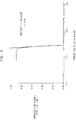
- the sensitivity and contrast of this formulation at 254 nm were determined to be approximately 3 mJ/cm2 and 9 respectively as are show in Fig. 2.
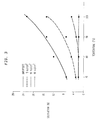
- the amount of silicon incorporated into a resist film is strongly influenced by the silylation temperature. This was studied by using IR spectroscopy to measure silicon uptake as a function of silylation temperature and exposure dose.
- the resist formulation of Example 1 was spin coated onto NaCl substrates and baked. The coated substrates were divided into four sets, the 1st set was exposed to 5 mJ/cm2, the 2nd set was exposed to 10 mJ/cm2, the 3rd set was exposed to 16 mJ/cm2, and the 4th set was unexposed. The wafers were baked at 120°C for 4 minutes and were silylated with dimethylaminotrimethylsilane for 5 minutes at 27, 103Pa (200 Torr) at various reaction temperatures.
- Fig. 3 provides plots showing that the percent silylation (as determined by IR spectroscopy) increases with temperature and decreases with UV exposure dose.
- Example shows the influences that silylation temperature has on the quality of the developed relief image.
- the formulation was coated onto 12 cm diameter silicon wafers and was processed as described above in Example(s) 1 and 2.
- the process conditions were held constant except for changes in the silylation temperature which was varied from 70 to 100°C.
- the higher the temperature during silylation the greater the degradation of the quality of the relief image.
- a top surface imageable resists was prepared by adding 9-phenoxymethylanthracene, an opaquing agent, to the resist composition of Example 1.
- the composition of the system was as follows: 17% (wt/wt) poly(p-hydroxystyrene-co-p-acetoxymethylstyrene), 0.9% (wt/wt) 9-phenoxymethylanthracene, 0.9% (wt/wt) triphenylsulfonium trifluoromethylsulfonate, and 81.2% (wt/wt) propylene glycol monomethyl ether acetate (PMA).
- This photoresist composition was spin coated at 3000 rpm onto silicon wafers to form a coating 0.8 ⁇ m thick coating.
- the coated wafers were baked at 90°C for 1 minute and were then exposed with 3.5 mJ/cm2 of deep UV light using a 1X Ultratech step-and-repeat tool (model X-248E) operating at 248 nm with a 7 nm wide band pass filter.
- the exposed wafers were then silylated for 2 minutes at 70°C using 27, 103Pa (200 Torr) of dimethylaminotrimethylsilane in a MONARCH single wafer silylation tool.
- the silylated wafers were transferred to a Materials Research Corporation magnetically enhanced plasma etch tool (model # MIE 710).
- etching conditions were as follows: 1kW RF power, 10 SCCM O2, 133.3 10 ⁇ 3Pa (1.0 mTorr), and an etch time of 1.2 minutes.
- the wafer was rinsed with 6:1 buffered HF, followed by water to remove a small amount of substrate residue.
- Fig. 5 shows the relief image generated in this process.
- This diacetate was compounded into a photoresist formulation such that there was 14.40% ( w / w ) poly(p-hydroxystyrene), 1.00% ( wt / wt ) 2,6-diacetoxymethyl- p-cresol, 1.15% ( w / w ) 9- anthracenemethanol, 81.99% ( w / w ) propylene glycol methyl ether acetate and 1.44% ( w / w ) MDT (trifluoromethylsulfonyloxy-bicyclo- [2.2.1]-hept-5-ene-2,3-dicarboximide), the non-metallic sulfonic acid precursor of EP Patent Application No.
- This photoresist formulation was spin coated onto silicon wafers to form a 1.1 ⁇ m thick coating.
- the coated wafers were baked at 90°C for 1 minute and were then exposed with 4.0 mJ/cm2 of 248nm light using a 0.37 NA CANON excimer step and repeat tool.
- the wafers were post-exposed baked on a 110°C hot-plate for 12 seconds.
- the wafers were then silylated for three minutes at 60°C using 13.3 10 ⁇ 3(100 Torr) dimethylaminotri- methylsilane in a MONARCH 150 single wafer silylation tool.
- the silylated wafers were etched in an Applied Materials AME5000 magnetically enhanced plasma etch tool. Etching conditions were as follows: 500 W RF power, 20 SCCM O2, 7 Pa (50 mTorr), 60 Gauss for 90 seconds. Etch residue was removed from the wafers with a 10 second immersion in 7:1 BHF followed by a water rinse (Fig. 6). Imaging at 365 ⁇ m was also accomplished with this resist system using GCA 0.45NA step and repeat tool. A dose of 20 mJ/cm2 was used for imaging (Fig. 7).
Landscapes
- Physics & Mathematics (AREA)
- General Physics & Mathematics (AREA)
- Spectroscopy & Molecular Physics (AREA)
- Chemical & Material Sciences (AREA)
- Chemical Kinetics & Catalysis (AREA)
- Inorganic Chemistry (AREA)
- Organic Chemistry (AREA)
- Materials For Photolithography (AREA)
- Photosensitive Polymer And Photoresist Processing (AREA)
- Exposure And Positioning Against Photoresist Photosensitive Materials (AREA)
Abstract
Description
- The present invention relates to processes for forming lithographic patterns with dry-developable, top surface imageable photoresist compositions.
- There has been a continuing desire in the electronics industry to obtain higher circuit density in microelectronic devices. To achieve the higher degree of integration necessary to meet the ground rules for such devices, lithographic techniques have been subjected to improvements which enhance the resolution of lithographic patterns in photoresist films.
- Aqueous base developable photoresist compositions which crosslink through electrophilic aromatic substitution have been disclosed in Reck et al., SPIE Regional Technical Conference on Photopolymers, Ellenville, NY, 63 (1988). Such formulations are characterized by having 3 structural components which include (a) an aromatic moiety, such as poly(4-hydroxystyrene) or novolak, which is susceptible to electrophilic aromatic substitution and allows for development under ionizing conditions, (b) a stable substance which is capable upon reaction with acid, of generating an electrophile, viz., a carbocationic species whose precursor is the acetate of an aryl methylol, and (c) a photo-acid generator which is an onium salt such as triphenylsulfonium hexafluoroantimonate. Upon exposure latent images are formed consisting of a strong acid dispersed in the exposed areas of the resist film. When the film is baked briefly after exposure, the acid cleaves the acetate group of the latent electrophile to produce a benzylic carbocationic species which reacts immediately with the surrounding phenolic resin to form new carbon-carbon bonds. Such formation of new carbon-carbon bonds results in an increase in molecular weight of the resin or its crosslinking, thereby drastically altering its solubility properties. Subsequent development in dilute base affords a negative-tone image of the mask. (Systems which included novolak resins were said to exhibit an unacceptable high optical density in deep UV).
- In Schellekens et al., Proc. SPIE 1086, 220 (1989), single layer resist systems are provided that involve the gas phase silylation and dry development of diazoquinone novolak resists and poly(vinylphenol) resists in the novolak case a novolak identified as AZ-Protective Coating was used and 2,6-bis(hydroxymethyl)-4-t-butyl-1-hydroxybenzene was used as a crosslinking agent and diphenyliodonium hexafluorophosphate was used as the deep UV sensitizer. In the case of the poly(vinylphenols), hexamethoxymethylmelamine was used as the crosslinker and 2(4-phenyl-phenyl)-4,6-bis(trichlorolmethyl)-s-triazine was used as the sensitizer. The authors of this paper took the position that the crosslinking both in the case of the novolak species and in the case of the poly(vinylphenols) occurs due to an esterification mechanism. The crosslinking sites are the hydroxy groups on the polymer chain. This paper further discloses the silylation of the resists using both hexamethyl disilazane and trimethylsilyldimethylamine as silylating agents.
- US-A- 4.613.398 to Chiong et al. is directed to methods for formation of etch resistant resists through the preferential permeation of organometallic materials into the differentially exposed polymeric resist materials. In certain embodiments, the differential permeation is achieved through the crosslinking of the polymer molecules to increase the molecular weight of the polymer and reduce its permeability. Typical of the photocrosslinkable polymers are those which contain functional groups such as hydroxy, carbonyl, phenol, amine and imide NH. These polymers include novolak resins, resoles, epoxides, and polymers containing azido groups and polyviynylphenol additionally crosslinking maybe through polyfunctional monomers and prepolymers containing double bonds and epoxy groups.
- US-A- 4.810.601 to Allen et al. is concerned with the formation of top surface images in resist films that transfers the image to only the top surface of the film so that the subsequent treatment with organometallic reagent occurs only in the top fraction of the film which is more permeable or more reactive to the organometallic reagent giving a structure which is equivalent to a bi or multilayer system. That disclosure is directed primarily to those materials which have recurrent acid labile pendent groups that when released from the polymer chain provide sights for reaction with the organomatallic material.
- The present invention relates to processes for generating positive tone resist images on a substrate comprising the steps of:
- (a) coating the substrate with a film comprising (i) a film-forming aromatic polymer resin having functional groups which activate said resin to stabilize said resin to electrophilic aromatic substitution, (ii) an acid catalyzable crosslinking agent which forms a carbonium ion upon reaction with acid, and (iii) a radiation degradable acid generator which is adapted to absorb imaging radiation, such that, upon crosslinking, said composition is more highly densified and us less permeable to the absorption of an organometallic reagent in the crosslinked regions than it is in the non-crosslinked regions;
- (b) imagewise exposing of the film to mid or deep UV radiation to cause densification of the resin in the exposed portion of the film;
- (c) contacting said film with an organometallic reagent to absorb the organometallic agent in such more permeable unexposed areas; and,
- (d) etching the film with reactive ions to yield a positive resist pattern.
- In the preferred embodiment of the invention the carbonium ion formed is a benzyl carbonium ion.
- In an alternative embodiment of the present invention, an aromatic dye may be included in the composition.
- A more thorough disclosure of the present invention is presented in the detailed description which follows and in the accompanying drawings.
- Fig. 1 is a photo micrograph showing images made by the process of the invention.
- Fig. 2 is a plot of sensitivity and constrast using the process of the invention.
- Fig. 3 is a plot showing percent silylation as a function of process terperature.
- Fig. 4 is a comparison of image degradation as a function of silylation terperature.
- Fig. 5 shows an image profile made using a dyed photoresist.
- Fig. 6 shows deep UV imaging of a photoresist using monomeric crosslinking agents.
- Fig. 7 shows i-line imagaing of a photoresist using monomeric crosslinking agents.
- The present invention relates to processes for generating positive tone resist images on a substrate comprising the steps of:
- (a) coating the substrate with a film comprising (i) a film-forming aromatic polymer resin having functional groups which activate said resin to electrophilic aromatic substitution, (ii) an acid catalyzable crosslinking agent which forms a carbonium ion upon reaction with acid, and (iii) a radiation degradable acid generator which is adapted to absorb imaging radiation, such that, upon crosslinking, said composition is more highly densified and us less permeable to the absorption of an organometallic reagent in the crosslinked regions than it is in the non-crosslinked regions;
- (b) imagewise exposing of the film to mid or deep UV radiation to cause crosslinking of the resin in the exposed portion of the film;
- (c) contacting said film with an organometallic reagent to absorb the organometallic agent in such more permeable unexposed areas; and,
- (d) etching the film with reactive ions to yield a positive resist pattern.
- In the first step of the process of the present invention, a suitable substrate such as silicon, silicon oxide, silicon nitride or galium arsenide is coated with a film comprising the resist composition which is dissolved in a suitable organic solvent.
- The aromatic polymer resin has functional groups which are preferably phenolic hydroxy groups, which activate the aromatic ring to electrophilic aromatic substitution. Typically such aromatic polymer resins will be activated ring systems such a polyhydroxystyrene or novolak resins. These materials include copolymers thereof and should be considered to comprise poly(hydroxystyrene), poly(hydroxystyrene-co-t-butyloxycarbonyloxystyrene), poly(hydroxystyrene-co-hydroxymethylstyrene), poly(hydroxystyrene-co-acetoxymethylstyrene) alkyl substituted polyvinyl phenols and novolak resins such as cresol novolak, ethylphenol novolaks, xylenol novolaks, etc.
- The acid catalyzable crosslinking agent is carbonium ion precursor. The preferred carbonium ions are benzylic carbonium ions, that is, phenyl methyl in form, and more than one carbonium ion site may be present on the precursor. Typical functional groups which react with acid to form carbonium ions are acetate groups on benzyl acetate type structures. The aromatic ring may be part of a polymer chain an be monomeric and may contain substituents which promote the formation and stabilization of the carbonium ion. The substituents must however be compatible with the imaging and stability characteristics of the final resist formulation. Preferred substituents include hydroxy (-OH), lower alkyl (preferably -CH₃), and substituted lower alkyl (preferably -CH₂OAc, where OAc is acetate).
- The crosslinking agents include poly-functional aromatic polymers which react with acid to form benyzl carbonium ions. The polymers need not have functional precursor groups on each aromatic ring. The preferred polymer structures are poly acetoxymethylstyrene and copolymers thereof. The most preferred copolymers are poly(acetoxymethyl- styrene-co-hydroxystyrene) polymers. Para orientation is preferred and the ratio of hydroxystyrene to acetoxymethyl styrene is 4 to 1.
- The useful monomeric crosslinking agents are of the form of diacetoxymethyl phenolic monomers. It has been found that having the acetoxymethyl groups in the ortho position with respect to a phenolic hydroxy group promotes stabilized carbonium ions. The preferred monomeric carbonium ion precursors include 2,6-diacetoxymethyl-p-cresol, 2,6-diacetoxymethylphenol, 2,2',6,6'-tetracetoxy methyl-Bisphenol A and trisacetoxy mestylene.
- Suitable photoacid generators for use in the present invention include radiation degradable acid generators (sometimes known as photoacids). These photoacids include metallic and non-metallic onium salts and non-metallic sulfonic acid precursors which generate strong acids upon exposure to radiation. Typical of the onium salts are diaryliodonium and triarylsulfonium salts. These photoacids may include diphenyliodonium hexafluoroarsenate, di(t-butyphenyl)iodonium hexafluoroarsenate, diphenyliodonium hexafluoroantimonate, di(t-butylphenyl)iodonium hexafluoroantimonate, diphenyliodonium triflate, di(t-butylphenyl)iodonium triflate, triphenylsulfonium hexafluoroantimonate, tri(t-butylphenyl)sulfonium hexafluoroantimonate, triphenylsulfonium hexafluoroarsinate, tri(t-butylphenyl)sulfoninium hexafluoroasenate, triphenylsulfonium hexafluorophosphate, tri(t-butyl-phenyl)sulfonium hexafluorophosphate, triphenylsulfonium triflate and tri(t-butylphenyl) sulfonium triflate.
- Among the non-metallic sulfonic acid precursors which generate strong acids upon exposure to radiation are N-sulfonyloxyimides of the form

where R is selected from the group consisting of -CF₃, - CF₂CF₃, -CF₂CF₂H, -(CF₂)n-Z where n = 1 to 4, where Z is H, alkyl, aryl,

where m = 1 to 5, where X any Y either (1) form a cyclic or polycyclic ring which may contain one or more hetero atoms, (2) form a fused aromatic ring, (3) may be independently H, alkyl or aryl, (4) may be attached to another sulfonyloxyimide-containing residue, or (5) may be attached to a polymeric chain or backbone. - The film may also comprise an aromatic dye which functions to absorb substantially all imaging mid and deep UV radiation incident on the film during the process before it reaches the substrate. The imaging mid and deep UV radiation used to process the present invention preferably has a wave length of from about 200 to about 370 nm. Suitable dyes include phenoxymethyl anthracene, anthracenemethanol, 9,10-diphenylanthracene, and phenanthracene and biphenyl derivatives.
- In the second step of the process of the present invention, the film is imagewise exposed to mid or deep UV radiation to densify the aromatic polymer in the exposed region of the film. Suitable radiation sources include various arc lamps as mercury, deuterium or excimer laser source.
- In the third step of the process of the present invention, the film is contacted with an organometallic agent in liquid or gas phase. The preferred metallic portions of the organometallic agent comprise silicon, tin, gemanium and titanium. Preferred organometallic compounds are organosilicon and organostannyl compounds including, for example dimethylaminotrimethylsilane, hexamethyldisilazane, trimethylsilylchloride, trimethylstannylchloride and 1,1,3,3,5,5-hexamethylcyclotrisilazane. Other organometallic agents will be known to those skilled in the art.
- The un-crosslinked portions of the resists film absorb the organometallic compound to provide the film with resistance to O₂ reactive ion etching.
- The final step of the process of the present invention involves reactive ion etching of the film to yield positive tone dry-developed images etching techniques and etching agents and equipment are well known in the art. In the present invention it is preferred that the etching plasma be an O₂ plasma.
- The following examples are detailed descriptions of methods of preparation and use of the process of the present invention. The detailed preparations fall within the scope of, and serve to exemplify, the more generally described methods set forth above. The examples are presented for illustrative purposes only, and are not intended to restrict or limit the scope of the invention.
- 2.0g of poly (p-hydroxystrene-co-p-acetoxymethylstyrene) having approximately 8 p-hydroxy- styrene groups to 2 p-acetoxymethylstyrene groups and 0.10g of triphenylsulfonium hexfluoroarsenate were formulated as a photoresist having 18 weight % of solids in propylene glycol monomethyl ether acetate (PMA). This photoresist mixture was spin coated at 4.000 rpm onto silicon wafers to form a coating 1.0 µm thick and the coated wafers were baked at 90°C for four minutes on a hot plate. The coated wafers were exposed to 16 mJ/cm² of deep UV radiation using a Perkin-Elmer Micraline 500 operating in the UV-2 mode. The exposed wafers were baked on a hotplate for 3 minutes at 120°C . The exposed wafers were then silylated for 5 minutes at 70°C using 27, 10³Pa (200 Torr) of dimethylaminotrimethylsilane. The silylated wafers were transferred to a Plasma-Therm parallel plate reactive ion etch tool for O₂ plasma development of the relief image. The etching conditions were as follows: 150 watts RF power, 40 SCCM O₂, 2,7 Pa (20 mTorr) and etch time of 30 minutes. The relief image generated in this Example is shown in Fig. 1.
- The sensitivity and contrast of this formulation at 254 nm were determined to be approximately 3 mJ/cm² and 9 respectively as are show in Fig. 2.
- The amount of silicon incorporated into a resist film is strongly influenced by the silylation temperature. This was studied by using IR spectroscopy to measure silicon uptake as a function of silylation temperature and exposure dose. In this Example the resist formulation of Example 1 was spin coated onto NaCl substrates and baked. The coated substrates were divided into four sets, the 1st set was exposed to 5 mJ/cm², the 2nd set was exposed to 10 mJ/cm², the 3rd set was exposed to 16 mJ/cm², and the 4th set was unexposed. The wafers were baked at 120°C for 4 minutes and were silylated with dimethylaminotrimethylsilane for 5 minutes at 27, 10³Pa (200 Torr) at various reaction temperatures. Fig. 3 provides plots showing that the percent silylation (as determined by IR spectroscopy) increases with temperature and decreases with UV exposure dose.
- This Example shows the influences that silylation temperature has on the quality of the developed relief image. In this study the formulation was coated onto 12 cm diameter silicon wafers and was processed as described above in Example(s) 1 and 2. The process conditions were held constant except for changes in the silylation temperature which was varied from 70 to 100°C. As may be seen from Fig. 4, the higher the temperature during silylation, the greater the degradation of the quality of the relief image.
- A top surface imageable resists was prepared by adding 9-phenoxymethylanthracene, an opaquing agent, to the resist composition of Example 1. The composition of the system was as follows: 17% (wt/wt) poly(p-hydroxystyrene-co-p-acetoxymethylstyrene), 0.9% (wt/wt) 9-phenoxymethylanthracene, 0.9% (wt/wt) triphenylsulfonium trifluoromethylsulfonate, and 81.2% (wt/wt) propylene glycol monomethyl ether acetate (PMA). This photoresist composition was spin coated at 3000 rpm onto silicon wafers to form a coating 0.8 µm thick coating. The coated wafers were baked at 90°C for 1 minute and were then exposed with 3.5 mJ/cm² of deep UV light using a 1X Ultratech step-and-repeat tool (model X-248E) operating at 248 nm with a 7 nm wide band pass filter. The exposed wafers were then silylated for 2 minutes at 70°C using 27, 10³Pa (200 Torr) of dimethylaminotrimethylsilane in a MONARCH single wafer silylation tool. The silylated wafers were transferred to a Materials Research Corporation magnetically enhanced plasma etch tool (model # MIE 710). The etching conditions were as follows: 1kW RF power, 10 SCCM O₂, 133.3 10⁻³Pa (1.0 mTorr), and an etch time of 1.2 minutes. The wafer was rinsed with 6:1 buffered HF, followed by water to remove a small amount of substrate residue. Fig. 5 shows the relief image generated in this process.
- Preparation of 2,6-diacetoxymethyl-p-cresol was accomplished in a quantitative manner by reaction of p-cresol with 2 equivalents of formaldehyde to form di-2,6-hydroxymethyl p-cresol which was further treated with acetic anhydride and sulfuric acid in acetic acid to form the diacetate(diester).
- This diacetate was compounded into a photoresist formulation such that there was 14.40% (w/w) poly(p-hydroxystyrene), 1.00% (wt/wt) 2,6-diacetoxymethyl- p-cresol, 1.15% (w/w) 9- anthracenemethanol, 81.99% (w/w) propylene glycol methyl ether acetate and 1.44% (w/w) MDT (trifluoromethylsulfonyloxy-bicyclo- [2.2.1]-hept-5-ene-2,3-dicarboximide), the non-metallic sulfonic acid precursor of EP Patent Application No. 9048016.6 filed 02 Feb, 1990, the disclosure of which is incorporated by reference into the present application. This photoresist formulation was spin coated onto silicon wafers to form a 1.1 µm thick coating. The coated wafers were baked at 90°C for 1 minute and were then exposed with 4.0 mJ/cm² of 248nm light using a 0.37 NA CANON excimer step and repeat tool. The wafers were post-exposed baked on a 110°C hot-plate for 12 seconds. The wafers were then silylated for three minutes at 60°C using 13.3 10⁻³(100 Torr) dimethylaminotri- methylsilane in a MONARCH 150 single wafer silylation tool. The silylated wafers were etched in an Applied Materials AME5000 magnetically enhanced plasma etch tool. Etching conditions were as follows: 500 W RF power, 20 SCCM O₂, 7 Pa (50 mTorr), 60 Gauss for 90 seconds. Etch residue was removed from the wafers with a 10 second immersion in 7:1 BHF followed by a water rinse (Fig. 6). Imaging at 365 µm was also accomplished with this resist system using GCA 0.45NA step and repeat tool. A dose of 20 mJ/cm² was used for imaging (Fig. 7).
- Although this invention has been described with respect to specific embodiments, the details thereof are not to be construed as limitations, for it will be apparent that various embodiments, changes and modifications may be resorted to without departing from the spirit and scope thereof, and it is understood that such equivalent embodiments are intended to be included within the scope of this invention.
Claims (24)
- A process for generating a positive tone resist image on a substrate comprising the steps of:(a) coating the substrate with a film comprising (i) a film-forming aromatic polymer resin having functional groups which activate said resin to stabilize said resin to electrophilic aromatic substitution, (ii) an acid catalyzable crosslinking agent which forms a carbonium ion upon reaction with acid, and (iii) a radiation degradable acid generator which is adapted to absorb imaging radiation, such that, upon crosslinking, said composition is more highly densified and is less permeable to the absorption of an organometallic reagent in the crosslinked regions than it is in the non-crosslinked regions;(b) imagewise exposing of the film to mid or deep UV radiation to cause densification of the resin in the exposed portion of the film;(c) contacting said film with an organometallic reagent to absorb the organometallic agent in such more permeable unexposed areas; and,(d) etching the film with reactive ions to yield a positive resist pattern.
- The process of Claim 1 wherein the carbonium ion formed is a benzyl carbonium ion.
- The process of Claim 1 wherein the organometallic reagent is in liquid or gaseous form.
- The process of Claim 3 wherein the organometallic reagent is selected from the group consisting of organosilicon, organotin, organogermanium and organotitanium compounds
- The process of Claim 4 wherein the organometallic reagent is dimethylaminotri- methylsilane, hexamethyldisilazane, trimethyl- silylchloride, trimethylstannychloride and 1,1,3,3,5,5-hexamethylcyclotrisilazane.
- The process of Claim 1 wherein the functional groups of said aromatic polymer resin are phenolic hydroxy groups.
- The process of Claim 1 wherein the aromatic polymer resin is selected from the group consisting of poly(hydroxystyrene), poly(hydroxystyrene-co-t-butyloxycarbonyl- oxystyrene), poly(hydroxy-styrene-co-hydroxy- methylstyrene), poly(hydroxystyrene-co-acetoxy- methylstyrene), and novolak resin.
- The process of Claim 7 wherein the novolak resin is an alkylphenolformaldehyde condensation product.
- The process of Claim 8 wherein the alkylphenol- formaldehyde condensation product is selected from the group consisting of cresol novolaks, ethylphenol novolaks, and xylenol novolaks.
- The process of Claim 1 wherein said acid catalyzable crosslinking agent which forms a benzyl carbonium ion upon reaction with acid is a polyfunctional monomer.
- The process of Claim 10 wherein said polyfunctional monomer is selected from the group consisting 2,6-diacetoxymethy-p- cresol, 2,6-diacetoxy phenol 2,2',6,6'tetra- acetoxymethyl-Bisphenol A, and trisacetoxy- mesitylene
- The process of Claim 1 wherein said acid catalyzable crosslinking agent which forms a benzyl carbonium ion upon reaction with acid is a polyfunctional polymer.
- The process of Claim 12 wherein said polyfunctional polymer is selected from the group consisting acetoxymethylstyrene and copolymers thereof.
- The process of Claim 13 wherein said polyfunctional polymer is a copolymer of p-hydroxystyrene and p-acetoxymethyl styrene where the molecular ratio of p-hydroxystyrene to p-acetoxymethyl styrene is about 4 to 1.
- The process of Claim 1 wherein the radiation degradable acid generator which is adapted to absorb imaging radiation is selected from the group consisting of metallic and nonmetallic onium salts and non-metallic sulfonic acid precursors which generate strong acids upon exposure to radiation.
- The process of Claim 15 wherein the onium salts are selected from the group consisting of diaryliodonium salts and triarylsulfonium salts.
- The process of Claim 16 wherein the diaryiodionium salts are selected from the group consisting of diaryliodonium hexafluoroarsenates, hexafluoroantimonates, and triflates.
- The process of Claim 17 wherein the diaryl- iodonium hexafluoroarsenates, hexafluoroan- timonates, and triflates are selected from the group consisting of diphenyliodonium hexafluoro- arsenate, di(t-butylphenyl)iodonium hexafluoroa- rsenate, diphenyliodonium hexafluoroantimonate, di(t-butyl-phenyl)iodonium hexafluoroan- timonate, diphenyliodonium triflate, and di(t-butylphenyl)iodonium triflate.
- The process of Claim 16 wherein the triarylsulfonium salts are selected from the group consisting of trialkylsulfonium hexaafluoroantimonates, hexafluoroarsenates, hexafluorophosphates, and triflates.
- The process of Claim 19 wherein the trialkylsulfonium hexafluoroantimonates, hexafluoroarsenates, hexafluorophosphates, and triflates are selected from the group consisting of triphenylsulfonium hexafluoroantimonate, tri(t-butylphenyl) sulfonium hexafluoroantimonate, triphenylsulfonium hexafluoroarsenate, tri(t-butylphenyl)sulfonium hexafluoroarsenate, triphenylsulfonium hexafluorophosphate, tri(t-butylphenyl)sulfonium hexafluorophosphate, triphenylsulfonium triflate, and tri(t-butyl-phenyl)sulfonium triflate.
- The process of Claim 15 wherein the non-metallic sulfonic acid precursors are N-sulfonyloxyimides of the form


- The process of Claim 1 which further includes an effective amount of an aromatic dye to absorb substantially all imaging electromagnetic radiation incident on said film during imaging.
- The process of Claim 22 wherein said aromatic dye is selected from the group consisting of nitrostilbene, and anthracene or a biphenyl.
- The process of Claim 23 wherein said anthracene is selected from the group consisting of phenoxymethyl anthracene, anthracene methanol, 9,10-diphenylanthracene, and phenanthracene.
Applications Claiming Priority (2)
| Application Number | Priority Date | Filing Date | Title |
|---|---|---|---|
| US07/796,527 US5322765A (en) | 1991-11-22 | 1991-11-22 | Dry developable photoresist compositions and method for use thereof |
| US796527 | 1991-11-22 |
Publications (2)
| Publication Number | Publication Date |
|---|---|
| EP0543762A1 true EP0543762A1 (en) | 1993-05-26 |
| EP0543762B1 EP0543762B1 (en) | 2000-02-16 |
Family
ID=25168399
Family Applications (1)
| Application Number | Title | Priority Date | Filing Date |
|---|---|---|---|
| EP92480163A Expired - Lifetime EP0543762B1 (en) | 1991-11-22 | 1992-10-23 | Dry developable photoresist compositions and method for use thereof |
Country Status (4)
| Country | Link |
|---|---|
| US (1) | US5322765A (en) |
| EP (1) | EP0543762B1 (en) |
| JP (1) | JP2669581B2 (en) |
| DE (1) | DE69230684T2 (en) |
Cited By (3)
| Publication number | Priority date | Publication date | Assignee | Title |
|---|---|---|---|---|
| EP0675410A1 (en) * | 1994-03-28 | 1995-10-04 | Wako Pure Chemical Industries Ltd | Resist composition for deep ultraviolet light |
| EP0834770A2 (en) * | 1996-10-07 | 1998-04-08 | Shipley Company LLC | Dyed photoresists and methods and articles of manufacture comprising same |
| WO2004001797A2 (en) * | 2002-05-23 | 2003-12-31 | Applied Materials, Inc. | Sensitized chemically amplified photoresist for use in photomask fabrication and semiconductor processing |
Families Citing this family (23)
| Publication number | Priority date | Publication date | Assignee | Title |
|---|---|---|---|---|
| KR960012630B1 (en) * | 1993-08-23 | 1996-09-23 | 현대전자산업 주식회사 | Fine pattern forming method of semiconductor device |
| US5705116A (en) * | 1994-06-27 | 1998-01-06 | Sitzmann; Eugene Valentine | Increasing the useful range of cationic photoinitiators in stereolithography |
| JPH09230606A (en) * | 1994-07-05 | 1997-09-05 | Matsushita Electric Ind Co Ltd | Fine pattern forming method |
| KR0174316B1 (en) * | 1994-07-05 | 1999-04-01 | 모리시다 요이치 | Method of forming micropatterns |
| JPH08146599A (en) * | 1994-11-24 | 1996-06-07 | Nec Corp | Photosensitive composition and fine pattern forming method using the composition |
| JP3579946B2 (en) * | 1995-02-13 | 2004-10-20 | Jsr株式会社 | Chemically amplified radiation-sensitive resin composition |
| US5648196A (en) * | 1995-07-14 | 1997-07-15 | Cornell Research Foundation, Inc. | Water-soluble photoinitiators |
| US5707783A (en) * | 1995-12-04 | 1998-01-13 | Complex Fluid Systems, Inc. | Mixtures of mono- and DI- or polyfunctional silanes as silylating agents for top surface imaging |
| US6136498A (en) * | 1996-06-28 | 2000-10-24 | International Business Machines Corporation | Polymer-bound sensitizer |
| US6200726B1 (en) | 1996-09-16 | 2001-03-13 | International Business Machines Corporation | Optimization of space width for hybrid photoresist |
| US5976770A (en) * | 1998-01-15 | 1999-11-02 | Shipley Company, L.L.C. | Dyed photoresists and methods and articles of manufacture comprising same |
| US6383712B1 (en) | 1998-06-05 | 2002-05-07 | International Business Machines Corporation | Polymer-bound sensitizer |
| US7704668B1 (en) * | 1998-08-04 | 2010-04-27 | Rohm And Haas Electronic Materials Llc | Photoresist compositions and methods and articles of manufacture comprising same |
| US6280911B1 (en) | 1998-09-10 | 2001-08-28 | Shipley Company, L.L.C. | Photoresist compositions comprising blends of ionic and non-ionic photoacid generators |
| US6200728B1 (en) | 1999-02-20 | 2001-03-13 | Shipley Company, L.L.C. | Photoresist compositions comprising blends of photoacid generators |
| US7255970B2 (en) * | 2005-07-12 | 2007-08-14 | Az Electronic Materials Usa Corp. | Photoresist composition for imaging thick films |
| JP6495025B2 (en) | 2014-01-31 | 2019-04-03 | ラム リサーチ コーポレーションLam Research Corporation | Vacuum integrated hard mask processing and equipment |
| JP6286227B2 (en) * | 2014-02-21 | 2018-02-28 | 富士フイルム株式会社 | Actinic ray-sensitive or radiation-sensitive resin composition, actinic ray-sensitive or radiation-sensitive film, mask blank provided with actinic ray-sensitive or radiation-sensitive film, pattern formation method, and electronic device manufacturing method |
| TWI753105B (en) * | 2017-02-22 | 2022-01-21 | 日商信越化學工業股份有限公司 | Pattern formation method |
| WO2020102085A1 (en) | 2018-11-14 | 2020-05-22 | Lam Research Corporation | Methods for making hard masks useful in next-generation lithography |
| KR20210095218A (en) * | 2018-12-20 | 2021-07-30 | 램 리써치 코포레이션 | dry development of resists |
| US20210011383A1 (en) * | 2019-07-12 | 2021-01-14 | Inpria Corporation | Stabilized interfaces of inorganic radiation patterning compositions on substrates |
| KR102431292B1 (en) | 2020-01-15 | 2022-08-09 | 램 리써치 코포레이션 | Bottom layer for photoresist adhesion and dose reduction |
Citations (5)
| Publication number | Priority date | Publication date | Assignee | Title |
|---|---|---|---|---|
| EP0204253A2 (en) * | 1985-06-06 | 1986-12-10 | International Business Machines Corporation | Formation of etch-resistant resists through preferential permeation |
| EP0248779A1 (en) * | 1986-05-08 | 1987-12-09 | U C B, S.A. | Process for producing positive patterns in a photoresist layer |
| EP0281182A1 (en) * | 1987-02-20 | 1988-09-07 | Koninklijke Philips Electronics N.V. | Method of manufacturing a semiconductor arrangement |
| EP0388343A2 (en) * | 1989-03-14 | 1990-09-19 | International Business Machines Corporation | Chemically amplified photoresist |
| EP0282724B1 (en) * | 1987-03-16 | 1990-12-12 | International Business Machines Corporation | Negative resist compositions |
Family Cites Families (15)
| Publication number | Priority date | Publication date | Assignee | Title |
|---|---|---|---|---|
| US4371605A (en) * | 1980-12-09 | 1983-02-01 | E. I. Du Pont De Nemours And Company | Photopolymerizable compositions containing N-hydroxyamide and N-hydroxyimide sulfonates |
| DE3107109A1 (en) * | 1981-02-26 | 1982-09-09 | Hoechst Ag, 6000 Frankfurt | LIGHT SENSITIVE MIXTURE AND COPY MATERIAL MADE THEREOF |
| US4810601A (en) * | 1984-12-07 | 1989-03-07 | International Business Machines Corporation | Top imaged resists |
| US4939070A (en) * | 1986-07-28 | 1990-07-03 | Brunsvold William R | Thermally stable photoresists with high sensitivity |
| US4863827A (en) * | 1986-10-20 | 1989-09-05 | American Hoechst Corporation | Postive working multi-level photoresist |
| JPH026566A (en) * | 1988-06-24 | 1990-01-10 | Mitsubishi Pencil Co Ltd | Pigment ink |
| US5079131A (en) * | 1988-08-29 | 1992-01-07 | Shipley Company Inc. | Method of forming positive images through organometallic treatment of negative acid hardening cross-linked photoresist formulations |
| KR900005226A (en) * | 1988-09-29 | 1990-04-13 | 윌리엄 비이 해리스 | Photosensitive composition and method of producing positive and negative phases |
| EP0361906A3 (en) * | 1988-09-29 | 1991-05-02 | Hoechst Celanese Corporation | Method of producing an image reversal negative photoresist having a photo-labile blocked imide |
| JPH02127645A (en) * | 1988-11-08 | 1990-05-16 | Fujitsu Ltd | Formation of positive type pattern |
| JPH036566A (en) * | 1989-06-02 | 1991-01-14 | Mitsubishi Electric Corp | Pattern forming method by excimer laser |
| JPH0383063A (en) * | 1989-08-28 | 1991-04-09 | Kanto Chem Co Inc | Pattern forming method |
| JPH03152543A (en) * | 1989-10-23 | 1991-06-28 | Internatl Business Mach Corp <Ibm> | Negative contrast photoresist developable by base |
| JPH03154058A (en) * | 1989-11-13 | 1991-07-02 | Fujitsu Ltd | Resin composition for silylation and formation of resist pattern by using the same |
| DE3943413A1 (en) * | 1989-12-30 | 1991-07-04 | Basf Ag | RADIATION-SENSITIVE MIXTURE AND METHOD FOR PRODUCING RELIEF STRUCTURES |
-
1991
- 1991-11-22 US US07/796,527 patent/US5322765A/en not_active Expired - Lifetime
-
1992
- 1992-10-21 JP JP4305898A patent/JP2669581B2/en not_active Expired - Fee Related
- 1992-10-23 EP EP92480163A patent/EP0543762B1/en not_active Expired - Lifetime
- 1992-10-23 DE DE69230684T patent/DE69230684T2/en not_active Expired - Lifetime
Patent Citations (5)
| Publication number | Priority date | Publication date | Assignee | Title |
|---|---|---|---|---|
| EP0204253A2 (en) * | 1985-06-06 | 1986-12-10 | International Business Machines Corporation | Formation of etch-resistant resists through preferential permeation |
| EP0248779A1 (en) * | 1986-05-08 | 1987-12-09 | U C B, S.A. | Process for producing positive patterns in a photoresist layer |
| EP0281182A1 (en) * | 1987-02-20 | 1988-09-07 | Koninklijke Philips Electronics N.V. | Method of manufacturing a semiconductor arrangement |
| EP0282724B1 (en) * | 1987-03-16 | 1990-12-12 | International Business Machines Corporation | Negative resist compositions |
| EP0388343A2 (en) * | 1989-03-14 | 1990-09-19 | International Business Machines Corporation | Chemically amplified photoresist |
Cited By (9)
| Publication number | Priority date | Publication date | Assignee | Title |
|---|---|---|---|---|
| EP0675410A1 (en) * | 1994-03-28 | 1995-10-04 | Wako Pure Chemical Industries Ltd | Resist composition for deep ultraviolet light |
| US5695910A (en) * | 1994-03-28 | 1997-12-09 | Wako Pure Chemical Industries, Ltd. | Resist composition for deep ultraviolet light |
| US5780206A (en) * | 1994-03-28 | 1998-07-14 | Wako Pure Chemical Industries, Ltd. | Fine pattern forming process using a resist composition sensitive to deep ultraviolet light |
| EP0834770A2 (en) * | 1996-10-07 | 1998-04-08 | Shipley Company LLC | Dyed photoresists and methods and articles of manufacture comprising same |
| EP0834770A3 (en) * | 1996-10-07 | 1999-07-21 | Shipley Company LLC | Dyed photoresists and methods and articles of manufacture comprising same |
| US7147983B1 (en) | 1996-10-07 | 2006-12-12 | Shipley Company, L.L.C. | Dyed photoresists and methods and articles of manufacture comprising same |
| WO2004001797A2 (en) * | 2002-05-23 | 2003-12-31 | Applied Materials, Inc. | Sensitized chemically amplified photoresist for use in photomask fabrication and semiconductor processing |
| WO2004001797A3 (en) * | 2002-05-23 | 2004-07-01 | Applied Materials Inc | Sensitized chemically amplified photoresist for use in photomask fabrication and semiconductor processing |
| US7067227B2 (en) | 2002-05-23 | 2006-06-27 | Applied Materials, Inc. | Sensitized chemically amplified photoresist for use in photomask fabrication and semiconductor processing |
Also Published As
| Publication number | Publication date |
|---|---|
| JP2669581B2 (en) | 1997-10-29 |
| US5322765A (en) | 1994-06-21 |
| JPH05232707A (en) | 1993-09-10 |
| DE69230684D1 (en) | 2000-03-23 |
| EP0543762B1 (en) | 2000-02-16 |
| DE69230684T2 (en) | 2000-08-17 |
Similar Documents
| Publication | Publication Date | Title |
|---|---|---|
| EP0543762B1 (en) | Dry developable photoresist compositions and method for use thereof | |
| JP4467857B2 (en) | Modification of 193nm photosensitive photoresist material by electron beam exposure | |
| US5296332A (en) | Crosslinkable aqueous developable photoresist compositions and method for use thereof | |
| USRE35821E (en) | Pattern forming method including the formation of an acidic coating layer on the radiation-sensitive layer | |
| EP0232972B1 (en) | Negative photoresist compositions and processes for preparing thermally stable, negative images using them | |
| US5017461A (en) | Formation of a negative resist pattern utilize water-soluble polymeric material and photoacid generator | |
| US6365322B1 (en) | Photoresist composition for deep UV radiation | |
| JP4799800B2 (en) | Chemically amplified negative photoresist composition | |
| JPS61144639A (en) | Radiation sensitive composition and pattern forming method using its composition | |
| WO2002006901A2 (en) | Photoresist composition for deep uv and process thereof | |
| EP1815296A1 (en) | A composition for coating over a phtoresist pattern | |
| US5384220A (en) | Production of photolithographic structures | |
| JP3441167B2 (en) | Photosensitive composition and pattern forming method using the same | |
| JPH02120366A (en) | Radiation-sensitive composition and formation of pattern by using same | |
| JP2607870B2 (en) | Image forming method | |
| JP3392728B2 (en) | Pattern formation method | |
| US7670749B2 (en) | Resist material and method for forming a patterned resist layer on a substrate | |
| JPH0547098B2 (en) | ||
| JPH01154047A (en) | Photosensitive composition | |
| JP2001249456A (en) | Negative type resist composition and resist pattern forming method | |
| JPH0980753A (en) | Photosensitive composition | |
| CN115873167A (en) | Resin and 193nm dry-process photoresist containing same | |
| JPH05281730A (en) | Resist composition | |
| JPH07191465A (en) | Positive resist composition for dry development | |
| JPH05267150A (en) | Formation of resist pattern |
Legal Events
| Date | Code | Title | Description |
|---|---|---|---|
| PUAI | Public reference made under article 153(3) epc to a published international application that has entered the european phase |
Free format text: ORIGINAL CODE: 0009012 |
|
| AK | Designated contracting states |
Kind code of ref document: A1 Designated state(s): DE FR GB |
|
| 17P | Request for examination filed |
Effective date: 19930918 |
|
| 17Q | First examination report despatched |
Effective date: 19970520 |
|
| GRAG | Despatch of communication of intention to grant |
Free format text: ORIGINAL CODE: EPIDOS AGRA |
|
| GRAG | Despatch of communication of intention to grant |
Free format text: ORIGINAL CODE: EPIDOS AGRA |
|
| GRAH | Despatch of communication of intention to grant a patent |
Free format text: ORIGINAL CODE: EPIDOS IGRA |
|
| GRAH | Despatch of communication of intention to grant a patent |
Free format text: ORIGINAL CODE: EPIDOS IGRA |
|
| GRAA | (expected) grant |
Free format text: ORIGINAL CODE: 0009210 |
|
| AK | Designated contracting states |
Kind code of ref document: B1 Designated state(s): DE FR GB |
|
| REF | Corresponds to: |
Ref document number: 69230684 Country of ref document: DE Date of ref document: 20000323 |
|
| ET | Fr: translation filed | ||
| PLBE | No opposition filed within time limit |
Free format text: ORIGINAL CODE: 0009261 |
|
| STAA | Information on the status of an ep patent application or granted ep patent |
Free format text: STATUS: NO OPPOSITION FILED WITHIN TIME LIMIT |
|
| 26N | No opposition filed | ||
| REG | Reference to a national code |
Ref country code: GB Ref legal event code: IF02 |
|
| PGFP | Annual fee paid to national office [announced via postgrant information from national office to epo] |
Ref country code: GB Payment date: 20031001 Year of fee payment: 12 |
|
| PG25 | Lapsed in a contracting state [announced via postgrant information from national office to epo] |
Ref country code: GB Free format text: LAPSE BECAUSE OF NON-PAYMENT OF DUE FEES Effective date: 20041023 |
|
| GBPC | Gb: european patent ceased through non-payment of renewal fee |
Effective date: 20041023 |
|
| PGFP | Annual fee paid to national office [announced via postgrant information from national office to epo] |
Ref country code: FR Payment date: 20101018 Year of fee payment: 19 |
|
| PGFP | Annual fee paid to national office [announced via postgrant information from national office to epo] |
Ref country code: DE Payment date: 20101028 Year of fee payment: 19 |
|
| REG | Reference to a national code |
Ref country code: FR Ref legal event code: ST Effective date: 20120629 |
|
| PG25 | Lapsed in a contracting state [announced via postgrant information from national office to epo] |
Ref country code: FR Free format text: LAPSE BECAUSE OF NON-PAYMENT OF DUE FEES Effective date: 20111102 |
|
| REG | Reference to a national code |
Ref country code: DE Ref legal event code: R071 Ref document number: 69230684 Country of ref document: DE |
|
| REG | Reference to a national code |
Ref country code: DE Ref legal event code: R071 Ref document number: 69230684 Country of ref document: DE |
|
| REG | Reference to a national code |
Ref country code: DE Ref legal event code: R081 Ref document number: 69230684 Country of ref document: DE Owner name: GLOBALFOUNDRIES INC., KY Free format text: FORMER OWNER: INTERNATIONAL BUSINESS MACHINES CORPORATION, ARMONK, NY, US Ref country code: DE Ref legal event code: R082 Ref document number: 69230684 Country of ref document: DE Representative=s name: RICHARDT PATENTANWAELTE PARTG MBB, DE Ref country code: DE Ref legal event code: R081 Ref document number: 69230684 Country of ref document: DE Owner name: GLOBALFOUNDRIES INC., KY Free format text: FORMER OWNER: INTERNATIONAL BUSINESS MACHINES CORPORATION, ARMONK, N.Y., US |
|
| REG | Reference to a national code |
Ref country code: DE Ref legal event code: R082 Ref document number: 69230684 Country of ref document: DE Representative=s name: RICHARDT PATENTANWAELTE PARTG MBB, DE Ref country code: DE Ref legal event code: R081 Ref document number: 69230684 Country of ref document: DE Owner name: GLOBALFOUNDRIES INC., KY Free format text: FORMER OWNER: GLOBALFOUNDRIES US 2 LLC (N.D.GES.DES STAATES DELAWARE), HOPEWELL JUNCTION, N.Y., US |
|
| REG | Reference to a national code |
Ref country code: FR Ref legal event code: TP Owner name: GLOBALFOUNDRIES INC., GB Effective date: 20160829 |