EP0489944A1 - Master-slave data communication method with flexible one-wire bus - Google Patents
Master-slave data communication method with flexible one-wire bus Download PDFInfo
- Publication number
- EP0489944A1 EP0489944A1 EP90123647A EP90123647A EP0489944A1 EP 0489944 A1 EP0489944 A1 EP 0489944A1 EP 90123647 A EP90123647 A EP 90123647A EP 90123647 A EP90123647 A EP 90123647A EP 0489944 A1 EP0489944 A1 EP 0489944A1
- Authority
- EP
- European Patent Office
- Prior art keywords
- address
- data
- slave
- telegram
- wire bus
- Prior art date
- Legal status (The legal status is an assumption and is not a legal conclusion. Google has not performed a legal analysis and makes no representation as to the accuracy of the status listed.)
- Granted
Links
- 238000000034 method Methods 0.000 title description 3
- 230000005540 biological transmission Effects 0.000 claims abstract description 32
- 230000015654 memory Effects 0.000 claims description 36
- 238000012360 testing method Methods 0.000 claims description 14
- 230000000903 blocking effect Effects 0.000 claims description 11
- 238000012545 processing Methods 0.000 claims description 8
- 230000001360 synchronised effect Effects 0.000 claims description 3
- 230000007704 transition Effects 0.000 claims description 3
- 238000011156 evaluation Methods 0.000 claims 1
- 230000002123 temporal effect Effects 0.000 claims 1
- 238000012546 transfer Methods 0.000 abstract description 4
- 230000006870 function Effects 0.000 description 9
- 230000008901 benefit Effects 0.000 description 7
- 238000010586 diagram Methods 0.000 description 7
- 238000005259 measurement Methods 0.000 description 5
- 238000005516 engineering process Methods 0.000 description 4
- 230000001419 dependent effect Effects 0.000 description 2
- 238000013461 design Methods 0.000 description 2
- 125000000524 functional group Chemical group 0.000 description 2
- 230000008569 process Effects 0.000 description 2
- 230000004913 activation Effects 0.000 description 1
- 230000008859 change Effects 0.000 description 1
- 230000008878 coupling Effects 0.000 description 1
- 238000010168 coupling process Methods 0.000 description 1
- 238000005859 coupling reaction Methods 0.000 description 1
- 238000001514 detection method Methods 0.000 description 1
- 230000010354 integration Effects 0.000 description 1
- 238000009420 retrofitting Methods 0.000 description 1
Images

Classifications
-
- H—ELECTRICITY
- H04—ELECTRIC COMMUNICATION TECHNIQUE
- H04L—TRANSMISSION OF DIGITAL INFORMATION, e.g. TELEGRAPHIC COMMUNICATION
- H04L12/00—Data switching networks
-
- H—ELECTRICITY
- H04—ELECTRIC COMMUNICATION TECHNIQUE
- H04L—TRANSMISSION OF DIGITAL INFORMATION, e.g. TELEGRAPHIC COMMUNICATION
- H04L12/00—Data switching networks
- H04L12/28—Data switching networks characterised by path configuration, e.g. LAN [Local Area Networks] or WAN [Wide Area Networks]
- H04L12/40—Bus networks
- H04L12/403—Bus networks with centralised control, e.g. polling
-
- H—ELECTRICITY
- H04—ELECTRIC COMMUNICATION TECHNIQUE
- H04L—TRANSMISSION OF DIGITAL INFORMATION, e.g. TELEGRAPHIC COMMUNICATION
- H04L12/00—Data switching networks
- H04L12/28—Data switching networks characterised by path configuration, e.g. LAN [Local Area Networks] or WAN [Wide Area Networks]
- H04L12/40—Bus networks
- H04L12/407—Bus networks with decentralised control
- H04L12/413—Bus networks with decentralised control with random access, e.g. carrier-sense multiple-access with collision detection (CSMA-CD)
- H04L12/4135—Bus networks with decentralised control with random access, e.g. carrier-sense multiple-access with collision detection (CSMA-CD) using bit-wise arbitration
Landscapes
- Engineering & Computer Science (AREA)
- Computer Networks & Wireless Communication (AREA)
- Signal Processing (AREA)
- Small-Scale Networks (AREA)
- Information Transfer Systems (AREA)
Abstract
Description
1. Die Erfindung betrifft ein Master-Slave-Datenübertragungssystem mit einem Master, der an einen Slave Daten sendet oder von dort abruft, wobei der Datentransfer über einen Eindraht-Bus mittels eines Telegramms erfolgt, das folgende Teilabschnitte enthält: einen Adreßteil, der die Datensenke oder die Datenquelle im Slave definiert, einen Datenteil, der entweder die gesendeten oder die abgerufenen Daten enthält und schließlich eine Start- und eine Endinformation, vgl. den Oberbegriff des Anspruchs 1.1. The invention relates to a master-slave data transmission system with a master that sends data to or retrieves data from a slave, the data being transferred via a single-wire bus by means of a telegram that contains the following subsections: an address part that stores the data sink or defines the data source in the slave, a data part that contains either the sent or the retrieved data and finally start and end information, cf. the preamble of
Ein derartiges Master-Slave-Datenübertragungssystem mit einem Eindraht-Bus ist an und für sich bekannt, beispielsweise auf dem Gebiet der Fernwirktechnik mit einem einzigen Datenübertragungskanal. Die konfliktfreie Steuerung des Eindraht-Busses erfordert im Falle von mehreren Mastern und/oder mehreren Slaves eine aufwendige Steuerschaltung, die man nur dann in Kauf nimmt, wenn zusätzliche Bus- und Steuerleitungen wegen der Entfernung unbedingt zu vermeiden sind. Der Fortschritt in der Integrationstechnik, insbesondere bei der monolithisch integrierten Schaltungstechnik, erlaubt es jedoch, bisher eher als passiv anzusehende Bauelemente mit "elektronischer Intelligenz" auszurüsten. Dies kann auch bei Datenübertragungssystemen, bei denen der Entfernungsgesichtspunkt weniger entscheidend ist, wie noch gezeigt werden wird, zu großen Vorteilen führen.Such a master-slave data transmission system with a single-wire bus is known per se, for example in the field of telecontrol technology with a single data transmission channel. In the case of multiple masters and / or multiple slaves, the conflict-free control of the single-wire bus requires an elaborate control circuit, which can only be accepted if additional bus and control lines must be avoided due to the distance. However, the progress in integration technology, especially in monolithically integrated circuit technology, has made it possible to equip components that were previously regarded as passive with "electronic intelligence". This can also lead to great advantages in data transmission systems where the distance point of view is less critical, as will be shown.
Es ist daher Aufgabe der in den Ansprüchen gekennzeichneten Erfindung, für ein Master-Slave-Datenübertragungssystem ein flexibles Eindraht-Bus-System anzugeben, das einen mehrfachen Master- und einen mehrfachen Slave Betrieb ermöglicht und dessen Datenformat an die jeweilige Übertragungs- und Betriebsanforderung optimal angepaßt werden kann.It is therefore an object of the invention characterized in the claims to provide a flexible single-wire bus system for a master-slave data transmission system, which has a multiple master and a multiple slave operation enables and whose data format can be optimally adapted to the respective transmission and operating requirements.
Die Lösung dieser Aufgabe erfolgt nach den im Kennzeichen des Anspruchs 1 angegebenen Merkmalen. Weitere, besonders vorteilhafte Ausführungen sind in abhängigen und unabhängigen Ansprüchen unter Schutz gestellt. Einige der Vorteile, die sich durch die Erfindung ergeben, sind im folgenden aufgeführt:This object is achieved according to the features specified in the characterizing part of
Die Flexibilität des Master-Slave-Datenübertragungssystems mit dem Eindraht-Bus ergibt sich im wesentlichen daraus, daß die einzelnen Elemente des Datenformats von Telegramm zu Telegramm sowohl in ihrer Anzahl als auch in sich variieren können.The flexibility of the master-slave data transmission system with the single-wire bus essentially results from the fact that the individual elements of the data format can vary from telegram to telegram, both in number and in themselves.
Ein Vorteil ergibt sich aus der frei wählbaren Adreßlänge, wodurch der rasche Zugriff auf wichtige Daten über eine Kurzadresse ermöglicht wird.One advantage results from the freely selectable address length, which enables quick access to important data via a short address.
Ein weiterer Vorteil ergibt sich bei Datenübertragungssystemen, die derartige Master und Slaves als austauschbare Bauelemente enthalten. Eine Anwendung findet sich beispielsweise im Kraftfahrzeugbereich, wenn ein oder mehrere als Master dienende Prozessoren aus räumlich auseinanderliegenden Sensoren, die als Slaves dienen, Daten abrufen müssen.A further advantage results in data transmission systems which contain such masters and slaves as interchangeable components. An application is found, for example, in the motor vehicle sector when one or more processors serving as masters have to call up data from spatially separated sensors that serve as slaves.
Neben der Einsparung von Datenleitungen - es genügt ein einziger Eindraht-Bus, an den alle Elemente angeschlossen sind - ist auch die Anzahl der Kontaktanschlüsse der jeweiligen Bauelemente ein wichtiger Gesichtspunkt. Je weniger Anschlußbeine und Verbindungsleitungen vorhanden sind, desto weniger besteht die Gefahr der Vertauschung oder des Ausfalls durch Leitungsunterbrechungen oder Kontaktprobleme.In addition to saving data lines - a single single-wire bus to which all elements are connected is sufficient - the number of contact connections of the respective components is also an important consideration. The fewer connecting legs and connecting lines there are, the less risk of confusion or failure due to line breaks or contact problems.
Die frei wählbare Adresslänge erleichtert auch den Austausch oder die Nachrüstung. Denn neue, zusätzliche Funktionen, die über längere Adressen als sogenannte Optionen abzurufen sind, kommen mit bisherigen Funktionen nicht in Konflikt, weil diese nach wie vor über die bisherigen, kürzeren Adressen abzurufen sind.The freely selectable address length also makes replacement or retrofitting easier. This is because new, additional functions that can be called up via longer addresses as so-called options do not conflict with previous functions because they can still be called up via the previous, shorter addresses.
Ein weiterer Vorteil ergibt sich aus der Einsparung von Anschlußbeinen bei selbständigen Bauelementen, die in einem derartigen System zusammengekoppelt sind. Im Extremfall läßt sich die Anzahl der Anschlußbeine von "intelligenten" Sensoren, Speichern, Gebern usw. bis auf drei reduzieren.Another advantage results from the saving of connecting legs in the case of independent components which are coupled together in such a system. In an extreme case, the number of connection legs of "intelligent" sensors, memories, transmitters etc. can be reduced to three.
Die Erfindung und ihre Vorteile werden nun anhand der Figuren der Zeichnung näher erläutert:
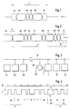
- Fig. 1 zeigt schematisch ein einfaches Format des Telegramms auf dem Eindraht-Bus,
- Fig. 2 zeigt schematisch ein erweitertes Format,
- Fig. 3 zeigt schematisch als Blockschaltbild drei Master und vier Slaves, die über einen Eindraht-Bus miteinander gekoppelt sind,
- Fig. 4 zeigt schematisch einen Telegrammausschnitt,
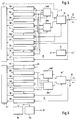
- Fig. 5 zeigt schematisch als Blockschaltbild die einzelnen Funktionsgruppen eines Masters in einer aufwendigen Ausführung,
- Fig. 6 zeigt als Blockschaltbild die einzelnen Funktionsgruppen eines Slaves in einer aufwendigen Ausführung,
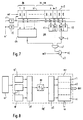
- Fig. 7 zeigt als Blockschaltbild schematisch eine Adreßlängen-Überprüfungseinrichtung,
- Fig. 8 zeigt als Blockschaltbild schematisch eine Mehrfachdatenquelle in einem Slave, die Teil eines Sensorbauelementes ist,
- Fig. 9 zeigt schematisch ein dreibeiniges Sensorbauelement,
- Fig. 10 zeigt schematisch als Blockschaltbild ein erstes Speicherbauelement und
- Fig. 11 zeigt schematisch ein dreibeiniges Speicherbauelement.
- 1 schematically shows a simple format of the telegram on the single-wire bus,
- 2 schematically shows an expanded format,
- 3 schematically shows a block diagram of three masters and four slaves, which are coupled to one another via a single-wire bus,
- 4 schematically shows a telegram section,
- 5 shows schematically as a block diagram the individual function groups of a master in a complex embodiment,
- Fig. 6 shows the individual as a block diagram Functional groups of a slave in a complex design,
- 7 schematically shows an address length checking device as a block diagram,
- 8 schematically shows a block diagram of a multiple data source in a slave, which is part of a sensor component,
- 9 schematically shows a three-legged sensor component,
- 10 schematically shows a first memory component and
- 11 schematically shows a three-legged memory component.
In Fig. 1 beginnt das Telegramm T mit einer Startinformation si. An dieses schließt sich ein in der Länge variable Adreßteil ad, eine erste Marke m1, ein Synchronisierbit sb, ein in der Länge variablen Teil dt und schließlich eine Endinformation oi an. Vor und nach dem Telegramm nimmt der Eindraht-Bus B (vgl. Fig. 3) einen Ruhe- oder Wartezustand ein. Im Ruhezustand wird der Eindraht-Bus entweder hochohmig geschaltet oder auf ein oberes oder unteres Schaltpotential gelegt, vgl. auch Fig. 4. Außerhalb des Telegramms T kann auf dem Eindraht-Bus ein Bittakt bt als Wartesignal übertragen werden. In diesem Fall kann die Übertragung spezieller Bits für die Start- und Endinformation si, oi entfallen. In bezug auf den Wartezustand mit gesendetem Bittakt ist die Startinformation si durch die letzte Bittaktperiode und die Endinformation oi durch zwei unmittelbar aufeinanderfolgende Bittaktperioden definiert. Zweckmäßigerweise ist die erste Marke ml und das Synchronisierbit sb jeweils ebenfalls nur eine Bittaktperiode lang. Fig. 4 zeigt, wie über unterschiedliche Tastverhältnisse die einzelnen Signale unterscheidbar sind.In Fig. 1, the telegram T begins with start information si. This is followed by an address part ad variable in length, a first label m1, a synchronization bit sb, a part dt variable in length and finally an end information item oi. Before and after the telegram, the single-wire bus B (cf. FIG. 3) assumes an idle or waiting state. In the idle state, the single-wire bus is either switched to high impedance or set to an upper or lower switching potential, cf. also Fig. 4. Outside the telegram T, a bit clock bt can be transmitted as a waiting signal on the single-wire bus. In this case, the transmission of special bits for the start and end information si, oi can be omitted. With regard to the wait state with the transmitted bit clock, the start information si is defined by the last bit clock period and the end information oi by two immediately consecutive bit clock periods. The first mark is expediently ml and that Synchronizing bit sb also only lasts for one bit clock period. FIG. 4 shows how the individual signals can be distinguished using different duty cycles.
In Fig. 2 ist schematisch ein aufwendigeres Telegramm T dargestellt, das jedoch sämtliche aus Fig. 1 bekannten Elemente enthält. Im Ruhe- oder Wartezustand außerhalb des Telegramms T wird vom Master ständig der Bittakt bt über den Eindraht-Bus gesendet. Das Ende des Bittaktes bt und der Beginn der Daten des Adreßteils ad bilden die Startinformation si. An den Adreßteil ad schließen sich wie in Fig. 1 die erste Marke m1, das Synchronisierbit sb und der in der Länge variable Datenteil dt an. Anders als in Fig. 1, in der nun die Endinformation oi folgt, zeigt eine zweite Marke m2 an, daß das Telegramm T noch nicht zu Ende ist. Es folgt ein ebenfalls in der Länge variabler Testteil tx, eine dritte Marke m3, ein Blockierbit bb und schließlich die Endinformation oi. Der Testteil tx dient der Überprüfung des Adreßteils ad und/oder Datenteils dt. Bei der Feststellung eines Fehlers wird der logische Zustand des Blockierbits bb geändert, wodurch die Ungültigkeit des gesamten übermittelten Telegramms T ausgelöst wird.FIG. 2 schematically shows a more complex telegram T, which however contains all the elements known from FIG. 1. In the idle or waiting state outside the telegram T, the master constantly sends the bit clock bt via the single-wire bus. The end of the bit clock bt and the start of the data of the address part ad form the start information si. As in FIG. 1, the address part ad is followed by the first mark m1, the synchronization bit sb and the data part dt, which is variable in length. Unlike in FIG. 1, in which the end information oi now follows, a second mark m2 indicates that the telegram T has not yet ended. This is followed by a test part tx, also variable in length, a third mark m3, a blocking bit bb and finally the final information oi. The test part tx is used to check the address part ad and / or data part dt. When an error is detected, the logical state of the blocking bit bb is changed, which triggers the invalidity of the entire transmitted telegram T.
Der Adreßteil ad - auch im Format von Fig. 1 - kann in eine Device-Adresse da, eine interne Adresse ia und in eine Operations-Adresse aufgespalten sein. Mittels der Device-Adresse da werden unterschiedliche Slaves angesprochen. Mittels der internen Adresse ia kann man innerhalb eines Slaves auf unterschiedliche Datenquellen oder Datensenken zugreifen. Die Operations-Adresse oa bestimmt, welche Operation im einzelnen der Slave ausführen soll. Ist der Slave beispielsweise ein Schreib-Lesespeicher, dann kann dieser Speicher mittels der speziellen Operations-Adresse oa für den Schreib- oder Lesebetrieb vorbereitet werden.The address part ad - also in the format of FIG. 1 - can be split into a device address, an internal address in general and an operation address. Different slaves are addressed using the device address. The internal address ia allows access to different data sources or data sinks within a slave. The operation address or the like determines which operation the slave should perform in detail. If the slave is a read-write memory, for example, then this memory can be prepared for the write or read operation by means of the special operation address or the like.
Das Synchronisierbit sb in Fig. 1 und Fig. 2 dient dazu, dem Master anzuzueigen, daß der Slave zur Übernahme des angefangenen Telegramms T momentan nicht bereit ist. Der Master gibt daraufhin den Eindraht-Bus durch Senden der Endinformation oi wieder frei und sendet das Telegramm T nach einer Wartezeit gegebenenfalls noch einmal.The synchronization bit sb in FIGS. 1 and 2 serves to indicate to the master that the slave is currently not ready to accept the telegram T that has started. The master then releases the single-wire bus by sending the end information oi and, if necessary, sends the telegram T again after a waiting time.
Wenn mehrere Master an den Eindraht-Bus angeschlossen sind, dann wird durch das Erkennen der Startinformation si die Aussendung eigener Telegramme T solange unterdrückt, bis die Endinformation oi auf dem Eindraht-Bus erscheint. Beginnen zufälligerweise gleichzeitig mehrere Master mit dem Senden von Telegrammen T, dann "verabschieden" sich nacheinander diejenigen Master, die mittels eines Ausgangsfehlerdetektors af (vgl. Fig. 5) einen Unterschied zwischen dem jeweils gesendeten und empfangenen Bit feststellen. Dies ist dadurch möglich, daß der Eindraht-Bus als "verdrahtete-ODER"-Verknüpfung ausgebildet ist. Hierbei ist einer der beiden Schaltzustände, in der Regel der L-Schaltzustand, bereits durch einen einzigen Master oder einen einzigen Slave zu erzwingen. Auf gleiche Weise wird der logische Zustand des Synchronisierbits sb und des Blockkierbits bb innerhalb der jeweiligen Bitperiode verändert. Die Prioritätssteuerung des Eindraht-Busses erfolgt somit auf einfache Weise durch den Ausgangsfehlerdetektor af.If several masters are connected to the single-wire bus, the recognition of the start information si suppresses the transmission of own telegrams T until the end information oi appears on the single-wire bus. If several masters coincidentally begin to send telegrams T, then those masters which "determine" a difference between the bit sent and received in each case by means of an output error detector af (cf. FIG. 5) "say goodbye". This is possible because the single-wire bus is designed as a "wired-OR" link. One of the two switching states, usually the L switching state, must already be enforced by a single master or a single slave. In the same way, the logical state of the synchronization bit sb and the block kier bit bb is changed within the respective bit period. The priority control of the single-wire bus is thus carried out in a simple manner by the output error detector af.
Die "verdrahdete-ODER"-Verknüpfung und der hochohmige Zustand (= Tristate-Zustand) können auch miteinander kombiniert werden. Dann befinden sich alle Master und Slaves bis auf die jeweils aktiven im hochohmigen Tristate-Zustand.The "wired-OR" link and the high-resistance state (= tristate state) can also be combined with one another. Then all masters and slaves except the active ones are in the high-resistance tristate state.
Wenn der aktive Master nach der Aussendung seines Telegramms im Wartezustand seinen Bittakt bt aussendet, dann prägt er allen anderen Mastern und Slaves seinen Bittakt so lange auf, bis sich ein neuer Master durch eine Startinformation si zu erkennen gibt und fortan die Taktführung übernimmt. In welchem Tastverhältnis der Bittakt bt während des Wartezustandes gesendet wird ist davon abhängig, wie die Erkennung des ersten Adreßbits erfolgt. Eventuell muß vor dem ersten Adreßbit eine logische "0", "1" oder eine Marke als Startinformation si eingeschoben werden.If the active master sends its bit clock bt in the waiting state after sending its telegram, it shapes all other masters and slaves Bit clock until a new master can be identified by start information si and henceforth takes over the clock management. The duty cycle in which the bit clock bt is sent during the wait state depends on how the first address bit is recognized. A logical "0", "1" or a label may have to be inserted as start information si before the first address bit.
Fig. 3 zeigt drei Master M, M1, M2 und vier Slaves S, S1, S2, S3, die über einen Eindraht-Bus B zusammengeschaltet sind. Dabei kann jeweils ein Master an einen Slave seriell über den Eindraht-Bus B Daten senden oder von dort abrufen. Die einzelnen Slaves sind dabei durch unterschiedliche Device-Adressen da unterscheidbar. Falls Daten auch zwischen den Mastern austauschbar sein sollen, müssen die ansprechbaren Master wie ein Slave adressier- und ansprechbar sein. Ein Slave S3 ist als Dreibeinelement dargestellt, wobei zwei Anschlüsse für die Versorgungsspannungen vorgesehen sind und der dritte Anschluß mit dem Eindraht-Bus B verbunden ist. Ein derartiges Bauelement ist beispielsweise ein elektronischer Temperaturfühler, dessen digitalisierter Temperaturwert über den Eindraht-Bus abgerufen wird.3 shows three masters M, M1, M2 and four slaves S, S1, S2, S3, which are interconnected via a single-wire bus B. A master can send data to a slave via the single-wire bus B or retrieve data from there. The individual slaves can be distinguished by different device addresses. If data should also be exchangeable between the masters, the addressable masters must be addressable and addressable like a slave. A slave S3 is shown as a tripod element, two connections being provided for the supply voltages and the third connection being connected to the single-wire bus B. Such a component is, for example, an electronic temperature sensor, the digitized temperature value of which is called up via the single-wire bus.
In Fig. 4 ist schematisch als Ausschnitt der Zeitverlauf eines Telegramms T mit zugehörigem Bittakt bt dargestellt. Vom Bittakt bt sind dabei lediglich die Taktperioden markiert, weil der eigentliche Signalverlauf, also das Tastverhältnis, an sich beliebig ist.4 schematically shows a section of the time profile of a telegram T with the associated bit clock bt. Only the clock periods are marked by the bit clock bt because the actual signal curve, that is to say the pulse duty factor, is in itself arbitrary.
Unter dem Bittakt bt ist der Signalverlauf einiger Bittaktperioden des Telegramms T dargestellt. Zu Beginn jeder Bittaktperiode findet ein Übergang vom L- in den H-Schaltzustand statt. Die negative Schaltflanke erfolgt zu bestimmten Zeiten während der Bittaktperiode und definiert innerhalb des Bittaktes unterschiedlich lange H- und L-Schaltzustände. Ein erstes bzw. zweites H/L-Tastverhältnis, das kleiner bzw. größer als 1 ist, definiert eine logische "0" bzw. "1". Ein drittes H/L-Tastverhältnis definiert die Marke mi und eventuell auch den Bittakt bt während des Wartezustandes.The signal curve of some bit clock periods of the telegram T is shown under the bit clock bt. At the beginning of each bit clock period there is a transition from the L to the H switching state. The negative switching edge occurs and is defined at certain times during the bit clock period H and L switching states of different lengths within the bit clock. A first or second H / L duty cycle, which is smaller or larger than 1, defines a logical "0" or "1". A third H / L duty cycle defines the mark mi and possibly also the bit clock bt during the waiting state.
Der Übergang vom Bittakt bt oder von den Marken mi auf ein Datenbit "0" oder "1" kennzeichnet die Startinformation si. Die Endinformation oi wird erkannt, wenn hintereinander mindestens zwei Marken mi gesendet werden. Das Synchronisierbit sb und das Blockierbit bb zeichnen sich dadurch aus, daß vom Master ein erster logischer Zustand, z.B. eine "1", gesendet wird. Wenn der Slave zur weiteren Abwicklung des Telegramms T bereit ist, dann behält er den logischen Zustand des Synchronisierbits sb bzw. des Blockierbits bb bei.The transition from the bit clock bt or from the marks mi to a data bit "0" or "1" characterizes the start information si. The end information oi is recognized if at least two marks mi are sent in succession. The synchronization bit sb and the blocking bit bb are characterized by the fact that a first logic state, e.g. a "1" is sent. If the slave is ready for further processing of the telegram T, it maintains the logical state of the synchronization bit sb or the blocking bit bb.
Wenn der Slave zur weiteren Abwicklung des Telegramms T indessen nicht bereit ist, dann löst er durch Umcodierung des Synchronisierbits in einen zweiten logischen Zustand, z.B. eine "0", im Master M ein Nichtbereitschaftssignal aus. Auf ähnliche Weise löst bei einem erkannten Fehler der Slave durch Umcodierung des Blockierbits bb in den zweiten logischen Zustand, z.B. "0", im Master M ein Ungültigkeitssignal aus. In beiden Fällen ist das gesendete Telegramm unwirksam, so daß es später wiederholt werden muß. Diese Zuweisung gilt für die "verdrahtete-ODER"-Verknüpfung, bei der sich eine "0" vor der "1" durchsetzt.If, however, the slave is not ready for further processing of the telegram T, it triggers by transcoding the synchronization bit into a second logic state, e.g. a "0", in the master M a non-ready signal. Similarly, if a fault is detected, the slave triggers by recoding the blocking bit bb into the second logic state, e.g. "0", in the master M an invalid signal. In both cases, the telegram sent is ineffective, so that it must be repeated later. This assignment applies to the "wired-OR" link, in which a "0" prevails over the "1".
Die erforderlichen Tastverhältnisse lassen sich am einfachsten von einem internen Systemtakt cl oder Hilfstakt ht (vgl. Fig. 5 und Fig. 6) ableiten, dessen Frequenz mindestens das Doppelte des Bittaktes bt beträgt. Die positiven Flanken des Telegramms T liefern den genauen Bittakt bt, an den sich in den Slaves und gegebenenfalls in den anderen Mastern alle Hilfstakt- und Taktgeneratoren phasengenau mit Hilfe von Phasenregelschleifen ankoppeln.The required duty cycle is easiest to derive from an internal system clock cl or auxiliary clock ht (see FIGS. 5 and 6), the frequency of which is at least twice the bit clock bt. The positive edges of the telegram T supply the exact bit clock bt that is in the slaves and possibly in Connect all auxiliary clock and clock generators to the other masters with phase accuracy using phase locked loops.
In Fig. 5 sind schematisch die einzelnen Funktionsgruppen eines Masters M dargestellt. Da die Funktionsgruppen für den Fachmann geläufige Schaltungen darstellen, erübrigt sich der besseren Übersichtlichkeit wegen eine ausführlichere Darstellung und Beschreibung. Den Zeitablauf und die Steuerung der einzelnen Funktionsgruppen übernimmt eine Master-Steuereinrichtung st, die aus den einzelnen Funktionsgruppen Steuersignale empfängt oder zu deren Aktivierung Steuersignale sendet.5 shows the individual functional groups of a master M schematically. Since the function groups represent circuits familiar to the person skilled in the art, a more detailed illustration and description is unnecessary for better clarity. The timing and the control of the individual function groups is undertaken by a master control device st, which receives control signals from the individual function groups or sends control signals for their activation.
Eine Ein-Ausgabestufe io ist mit ihrer Ausgangsklemme k mit dem Eindraht-Bus B verbunden und erzeugt die einzelnen H- und L-Schaltsignale im Sendebetrieb. Im Empfangsbetrieb werden die Schaltzustände des Eindraht-Busses B abgefühlt und einen Decodierer dec zugeführt. Eine eventuell vorgesehene Umsteuerung der Ein-Ausgabestufe io in einen hochohmigen Tristate-Zustand erfolgt durch ein Signal auf der gestrichelt dargestellten Steuerleitung f. Dem Decodierer dec für die empfangenen Signale entspricht der Codierer cod für die zu sendenden Signale - er steuert das Tastverhältnis der gesendeten Bits. Der Decodierer dec decodiert die empfangenen Signale bezüglich ihres Tastverhältnisses. Die entsprechenden Fenster werden durch eine Tastverhältnissteuerung tr, die mit den Steuereingängen des Codierers und Decodierers verbunden ist, gebildet.An input-output stage io is connected with its output terminal k to the single-wire bus B and generates the individual H and L switching signals in transmit mode. In the receive mode, the switching states of the single-wire bus B are sensed and a decoder dec is fed. Any changeover of the input / output stage io to a high-resistance tristate state is provided by a signal on the control line f shown in dashed lines. The decoder dec for the received signals corresponds to the encoder cod for the signals to be transmitted - it controls the pulse duty factor of the transmitted bits. The decoder dec decodes the received signals with respect to their duty cycle. The corresponding windows are formed by a duty cycle control tr, which is connected to the control inputs of the encoder and decoder.
Die Tastverhältnissteuerung tr steuert ferner einen Markengenerator mg, der über die Ein-Ausgabestufe io direkt die Marke mi für den Eindraht-Bus B bildet. Die seriellen Eingangsdaten für den Codierer cod stammen entweder aus einem Adressengenerator ag, einer Datenquelle dq oder einem Testdatengenerator tg. Die seriellen Ausgangsdaten des Decodierers dec werden entweder einer Datensenke ds, dem Testdatengenerator tg oder einem Stoppsignaldetektor sd zugeführt, dessen Vergleichseingang vom Markengenerator mg gespeist ist.The duty cycle control tr also controls a mark generator mg, which forms the mark mi for the single-wire bus B directly via the input-output stage io. The serial input data for the encoder cod come either from an address generator ag, a data source dq or a test data generator tg. The serial output data of the Decoders dec are either fed to a data sink ds, the test data generator tg or a stop signal detector sd, the comparison input of which is fed by the mark generator mg.
Stellt der Stoppsignaldetektor sd einen wesentlichen Unterschied im Tastverhältnis zwischen den beiden zugeführten Signalen fest, dann signalisiert er der Master-Steuereinrichtung st das Erkennen des Nichtbereitschafts- oder des Ungültigkeitssignals. Ähnlich arbeitet ein Fehlerdetektor fg, der an einem Eingang mit den Ausgangsdaten des Testdatengenerators tg und am anderen Eingang mit den Ausgangsdaten des Decodierers dec gespeist ist. Die Testdaten sind dabei aus den Adreßdaten und/oder den gesendeten oder empfangenen Daten gebildet, die dem Testdatengenerator zur Verrechnung zugeführt sind. Findet im Slave S eine gleiche Verrechnung der Daten zu Testdaten statt, dann wird über einen Vergleich der eigenen mit den empfangenen Testdaten mittels des Fehlerdetektors fd eine fehlerhafte Übertragung erkannt.If the stop signal detector sd detects a significant difference in the pulse duty factor between the two supplied signals, then it signals the master control device st to recognize the readiness signal or the invalid signal. An error detector fg works in a similar manner, which is fed at one input with the output data of the test data generator tg and at the other input with the output data of the decoder dec. The test data are formed from the address data and / or the sent or received data, which are fed to the test data generator for billing. If the same calculation of the data as test data takes place in slave S, then a faulty transmission is recognized by comparing the test data with the test data received by means of the error detector fd.
Eine andere Erkennung der Nichtbereitschafts- und Ungültigkeitssignale ermöglicht ein Ausgangsfehlerdetektor af, dessen erster Dateneingang an den Ausgang des Codierers cod und dessen zweiter Dateneingang an die Ausgangsklemme k der Ein-Ausgabestufe io angeschlossen ist. Sowie das Tastverhältnis an den beiden Abgriffen der Ein-Ausgabestufe io einen Unterschied zeigt, wird erkannt, daß ein Slave S das Synchronisier- oder Blockierbit sb, bb umcodiert hat.Another detection of the readiness and invalid signals is made possible by an output error detector af, the first data input of which is connected to the output of the encoder cod and the second data input of which is connected to the output terminal k of the input-output stage io. As soon as the pulse duty factor shows a difference at the two taps of the input / output stage, it is recognized that a slave S has recoded the synchronization or blocking bit sb, bb.
Als separater Block ist in Fig. 5 ein Taktgenerator tc dargestellt, der einen internen Systemtakt c1 erzeugt und dessen nicht dargestellte interne Phasenregelschleife an den Eindraht-Bus B angekoppelt oder von einem externen Systemtakt cl' gespeist ist. Die Versorgung des Eindraht-Busses B während des Wartezustandes mit dem Bittakt bt erfolgt durch den Markengenerator mg.5, a clock generator tc is shown as a separate block, which generates an internal system clock c1 and whose internal phase-locked loop (not shown) is coupled to the single-wire bus B or is fed by an external system clock cl '. The supply of the single-wire bus B during the waiting state with the bit clock bt is done by the mark generator mg.
Das Vorhandensein sämtlicher Funktionsgruppen im Master M ist für reduzierte Betriebsaufgaben nicht erforderlich. Sind beispielsweise nur Daten abzurufen, dann entfällt die Datenquelle dq. Der aufwendige Testdatengenerator tg, der auch im Slave erforderlich ist, entfällt, wenn die erforderliche Datenübertragungssicherheit gering oder auf andere Weise erreichbar ist, beispielsweise durch Wiederholung. Die Abwicklung des Datenformats nach Fig. 1 erfordert selbstverständlich ebenfalls keinen Testdatengenerator.The presence of all function groups in the Master M is not necessary for reduced operating tasks. If, for example, only data is to be called up, then the data source dq is omitted. The complex test data generator tg, which is also required in the slave, is omitted if the required data transmission security is low or can be achieved in some other way, for example by repetition. The processing of the data format according to FIG. 1 naturally also does not require a test data generator.
In Fig. 6 ist ein Slave S mit seinen einzelnen Funktionsblöcken schematisch dargestellt. Die funktionale Ähnlichkeit zum Master M kommt dabei auch in der zeichnischen Darstellung zum Ausdruck. Eine Ein-Ausgabestufe io' ist mit ihrer Ausgangsklemme k' an den Eindraht-Bus B angeschlossen. Der interne Datenausgang dieser Ein-Ausgabestufe ist an einen Decodierer dec' und der interne Dateneingang an den Ausgang eines Codierers cod' angeschlossen, der von einer Datenquelle dq' gespeist ist. Der Ausgang des Decodierers dec' ist auf eine Datensenke ds', einen Adressenkomparator al mit einer Adreßlängen-Überprüfungseinrichtung ue und einen Markendetektor md geführt.A slave S with its individual function blocks is shown schematically in FIG. 6. The functional similarity to Master M is also expressed in the drawing. An input-output stage io 'is connected to the single-wire bus B with its output terminal k'. The internal data output of this input-output stage is connected to a decoder dec 'and the internal data input is connected to the output of an encoder cod', which is fed by a data source dq '. The output of the decoder dec 'is routed to a data sink ds', an address comparator al with an address length checking device ue and a mark detector md.
Die Fenster für die verschiedenen Tastverhältnisse im Codierer cod' und Decodierer dec' sind von einer Tastverhältnissteuerung tr' gesteuert. Diese steuert auch das Tastverhältnis für das Nichtbereitschafts- und Ungültigkeitssignal, die in einem Stoppsignalgeber sg gebildet werden und direkt der Ein-Ausgabestufe io' zugeführt sind. Dort wird der zweite logische Zustand, also "0", dem jeweiligen Synchronisierbit sb oder Blockierbit bb zwangsweise aufgeprägt.The windows for the different duty cycles in the encoder cod 'and decoder dec' are controlled by a duty cycle controller tr '. This also controls the duty cycle for the non-readiness and invalid signal, which are formed in a stop signal generator sg and are fed directly to the input-output stage io '. There is the second logical state, so "0", the respective synchronization bit sb or blocking bit bb forced.
Das Vorhandensein eines Bittaktes bt auf dem Eindraht-Bus B während des Wartezustandes wird durch einen Bittaktdetektor bd erkannt, der bei Nichtvorhandensein des Bittaktes über einen Betriebsartumschalter bu, der auf die Slave-Steuereinrichtung st' einwirkt, einen stromsparenden Zustand auslöst. Ferner ist an dem Bittaktdetektor bd ein Hilfstaktgenerator hg angekoppelt, dessen Ausgangssignal ein Hilfstakt ht mit einem einfachen ganzzahligen Frequenzverhältnis zum Bittakt bt ist.The presence of a bit clock bt on the single-wire bus B during the waiting state is recognized by a bit clock detector bd which, in the absence of the bit clock, triggers a current-saving state via an operating mode switch bu which acts on the slave control device st '. Furthermore, an auxiliary clock generator hg is coupled to the bit clock detector bd, the output signal of which is an auxiliary clock ht with a simple integer frequency ratio to the bit clock bt.
Wenn der Slave S in CMOS-Technik ausgeführt ist, dann muß lediglich der interne Takt abgeschalten werden, um die Schaltung in einen stromlosen Zustand zu bringen.If the slave S is implemented in CMOS technology, then only the internal clock must be switched off in order to bring the circuit into a currentless state.
Im Adressenkomparator al, dem Adressen beliebiger Länge zugeführt werden können, befindet sich die Adreßlängen-Überprüfungseinrichtung ue. Bei Nichtübereinstimmung des Adreßteils ad (oder der Device-Adresse da) und der Adreßlänge unterbleibt die Aussendung eines Übernahmesignals aj (vgl. Fig. 7) an die Slave-Steuereinrichtung st'. Somit kann eine zufällige Adressenübereinstimmung in unterschiedlich langen Adressen nicht zur Übernahme führen.The address length checking device ue is located in the address comparator a1, to which addresses of any length can be supplied. If the address part ad (or the device address da) and the address length do not match, the transmission of a takeover signal aj (see FIG. 7) does not occur the slave control device st '. Thus, a random address match in addresses of different lengths cannot lead to the transfer.
Fig. 7 zeigt schematisch als Blockschaltbild ein Ausführungsbeispiel einer Adreßlängen-Überprüfungseinrichtung ue. Sie erfordert nur sehr wenig zusätzliche Bauelemente und besteht im wesentlichen aus dem sowieso vorhandenen Schieberegister sr, in dem die seriell zugeführten Daten des Adreßteils ad gespeichert sind.7 shows a block diagram of an exemplary embodiment of an address length checking device ue.It requires very little additional components and essentially consists of the shift register sr, which is present anyway and in which the serially supplied data of the address part ad are stored.
Das Schieberegister sr enthält zur Adreßlängenüberprüfung mindestens n+1 Schieberegisterstufen, wobei n die Stellenanzahl der zu erkennenden Adresse ist. Mittels eines Startsignals si', das aus der Startinformation si abgeleitet ist, werden spätestens zu Beginn des Einschreibvorgangs alle Schieberegisterstufen bis auf die erste auf "0" gesetzt; die erste Schieberegisterstufe wird auf "1" gesetzt. Das Setzen der einzelnen Schieberegisterstufen erfolgt über ihre Setz- und Rücksetzeingänge oder über ihre Dateneingänge, denen von einem ersten oder zweiten Speicher h1, h2 jeweils entweder eine "1" oder eine "0" zugeführt wird.The shift register contains sr for checking the address length at least n + 1 shift register levels, where n is the number of digits of the address to be recognized. By means of a start signal si ', which is derived from the start information si, all shift register stages except for the first are set to "0" at the latest at the start of the writing process; the first shift register level is set to "1". The individual shift register stages are set via their set and reset inputs or via their data inputs, to which either a "1" or a "0" is supplied from a first or second memory h1, h2.
Mit dem Beginn des Adreßteils ad beginnt das serielle Einlesen der Adressen in die einzelnen Schieberegisterstufen, das so lange andauert, bis die erste Marke m1 den Schiebevorgang beendet. Bei Übereinstimmung der Adressenlänge muß die gesetzte "1" der ersten Schieberegisterstufe in der Zwischenzeit bis in die (n+1)-te Schieberegisterstufe weitergeschoben worden sein. Als Kriterium für die richtigen Adreßenlänge dient die Überprüfung, daß eine erste "1" in der (n+1)-ten Schieberegisterstufe angekommen ist, und daß diese erste "1" auch dort noch vorhanden ist.With the beginning of the address part ad, the serial reading of the addresses into the individual shift register stages begins, which continues until the first mark m1 ends the shifting process. If the address length matches, the set "1" of the first shift register stage must in the meantime have been shifted into the (n + 1) th shift register stage. The criterion for the correct address length is the check that a first "1" has arrived in the (n + 1) th shift register stage and that this first "1" is still present there.
In dem dargestellten Ausführungsbeispiel nach Fig. 7 umfaßt die Schaltung für diese Überprüfung ein erstes und zweites RS-Flipflop f1, f2, zwei weitere Schieberegisterstufen n+1 und n+2, ein Inverter i und schließlich ein erstes und zweites UND-Gatter u1, u2. Mit dem Startsignal si' werden zu Beginn des Adreßlängen-Meßintervalls die Rücksetzeingänge R der beiden RS-Flipflops f1, f2 aktiviert. Der Setzeingang Set des ersten bzw. zweiten RS-Flipflops f1, f2 ist mit dem Ausgang der (n+1)-ten bzw. (n+2)-ten Schieberegisterstufe verbunden. Der Q-Ausgang des ersten bzw. zweiten RS-Flipflops f1, f2 ist mit einem Eingang des ersten UND-Gatters u1 direkt bzw. mit einem zweiten Eingang über den Inverter i verbunden. Ein weiterer Eingang des ersten UND-Gatters ist mit dem Ausgang eines Device-Adressenkomparators dk verbunden, dessen Paralleleingang von denjenigen Schieberegisterstufen gespeist ist, die die Device-Adresse da enthalten. Der Device-Adressenkomparator enthält die zu erkennende Device-Adresse als Hardware- oder Software-Information.7, the circuit for this check comprises a first and second RS flip-flop f1, f2, two further shift register stages n + 1 and n + 2, an inverter i and finally a first and second AND gate u1, u2. With the start signal si ', the reset inputs R of the two RS flip-flops f1, f2 are activated at the beginning of the address length measuring interval. The set input Set of the first and second RS flip-flops f1, f2 is connected to the output of the (n + 1) th and (n + 2) th shift register stage. The Q output of the first and second RS flip-flops f1, f2 is direct with an input of the first AND gate u1 or with one second input connected via the inverter i. Another input of the first AND gate is connected to the output of a device address comparator dk, the parallel input of which is fed by those shift register stages which contain the device address da. The device address comparator contains the device address to be recognized as hardware or software information.
Das Erkennen der richtigen Adressenlänge ergibt sich aus der Gültigkeitsüberprüfung folgender Schaltzustände:
- 1. Der Q-Ausgang des ersten RS-Flipflops f1 muß eine "1" aufweisen, das heißt, daß im Meßintervall mindestens einmal eine "1" in der (n+1)-ten Schieberegisterstufe war.
- 2. Der Q-Ausgang des zweiten RS-Flipflops f2 muß eine "0" aufweisen, das heißt, daß im Meßintervall bisher keine "1" in der (n+2)-ten Schieberegisterstufe war. Andernfalls wäre das zweite RS-Flipflop f2 in den anderen Zustand gekippt worden - dies wäre durch eine "1" am Q-Ausgang erkennbar.
- 3. Schließlich muß der Ausgang des Device-Adressenkomparators dk anzeigen, daß eine Übereinstimmung aller Stellen im Bereich der Device-Adresse da vorhanden ist.
- 4. Da die vorausgehenden Prüfungen 1 bis 3 erst dann das Übernahmesignal aj auslösen sollen, wenn die erste Marke m1 das Ende des Adreßteils ad signalisiert hat, wird die Wirksamkeit dieser Überprüfung von der ersten Marke m1 abhängig gemacht, indem ein von ihr abgeleitetes Signal m1' und das Ausgangssignal des ersten UND-Gatters u1 jeweils auf einen Eingang des zweiten UND-Gatters u2 geschaltet werden. Der Ausgang dieses UND-Gatters liefert das gewünschte Übernahmesignal aj.
- 1. The Q output of the first RS flip-flop f1 must have a "1", that is to say that there was at least one "1" in the (n + 1) th shift register stage in the measurement interval.
- 2. The Q output of the second RS flip-flop f2 must have a "0", which means that up to now there was no "1" in the (n + 2) th shift register stage in the measuring interval. Otherwise the second RS flip-flop f2 would have been flipped to the other state - this would be recognizable by a "1" at the Q output.
- 3. Finally, the output of the device address comparator dk must indicate that there is a match of all places in the area of the device address.
- 4. Since the preceding
tests 1 to 3 should only trigger the takeover signal aj when the first mark m1 has signaled the end of the address part ad, the effectiveness of this check is made dependent on the first mark m1 by a signal m1 derived from it 'and the output signal of the first AND gate u1 are each switched to an input of the second AND gate u2. The output of this AND gate supplies the desired takeover signal aj.
Die Überprüfung des Schaltzustandes der (n+1)-ten Schieberegisterstufe kann natürlich auch auf andere Weise erfolgen. Beispielsweise kann überprüft werden, ob das erste RS-Flipflop f1 erstmalig mit dem letzten Bittakt gekippt ist oder schon früher.The switching state of the (n + 1) th shift register stage can of course also be checked in another way. For example, it can be checked whether the first RS flip-flop f1 toggled for the first time with the last bit clock or earlier.
In Fig. 8 ist schematisch als Blockschaltbild eine Mehrfachdatenquelle dargestellt, die als Datenquelle dq' in einem Slave dient. Die eigentliche Datenquelle besteht dabei aus mehreren Analogsignalquellen q1, q2, qi, die von einem ersten Multiplexer p1 nacheinander abgetastet und einem Analog-Digitalumsetzer ac zugeführt werden. Dessen Ausgang speist den Eingang eines zweiten Multiplexers p2, der die Daten in die Speicherzellen r1, r2, ri einer Speichereinrichtung mr einschreibt. Das Auslesen der Daten dat der einzelnen Speicherzellen erfolgt durch Ansteuerung der jeweiligen Speicherzelle mittels der internen Adresse ia. Wenn in der Datenquelle dq' nur eine einzige Analogsignalquelle q1 vorhanden ist, dann entfällt natürlich der erste und zweite Multiplexer p1, p2 und die Speichereinrichtung mr benötigt nur eine einzige Speicherzelle r1, wobei die oben beschriebene Adressierung über die interne Adresse ia ebenfalls entfällt.FIG. 8 schematically shows a multiple data source as a block diagram, which serves as data source dq 'in a slave. The actual data source consists of several analog signal sources q1, q2, qi, which are sampled one after the other by a first multiplexer p1 and fed to an analog-digital converter ac. Its output feeds the input of a second multiplexer p2, which writes the data into the memory cells r1, r2, ri of a memory device mr. The data dat of the individual memory cells is read out by controlling the respective memory cell using the internal address ia. If only a single analog signal source q1 is present in the data source dq ', then of course the first and second multiplexers p1, p2 are omitted and the memory device mr only requires a single memory cell r1, the addressing described above via the internal address ia likewise generally being omitted.
Eine besonders vorteilhafte Anwendung von derartigen Master-Slave-Datenübertragungssystemen, in denen die Slaves als Datenquellen dq' eine einfache oder eine mehrfache Analogsignalquelle enthalten, findet sich in allen Arten von Sensorbauelementen für die unterschiedlichsten Meßaufgaben. Ihr Anschluß über den Eindraht-Bus B ermöglicht, daß eine Vielzahl von gleichen oder unterschiedlichen Sensorbauelementen über eine einzige Eindraht-Verbindung abgefragt werden können. Zusätzlich läßt sich die erforderliche Anzahl der Anschlußbeine der Sensorbauelemente im Extremfall bis auf drei Anschlüsse verringern, vgl. Fig. 3 und Fig. 9. Der erste Anschluß a1 dient der Verbindung mit dem Eindraht-Bus B. Der zweite und der dritte Anschluß a2, a3, dienen der Verbindung mit der positiven und negativen Versorgungsspannung.A particularly advantageous application of such master-slave data transmission systems, in which the slaves contain a single or a multiple analog signal source as data sources dq ', can be found in all types of sensor components for a wide variety of measurement tasks. Their connection via the single-wire bus B enables a large number of identical or different sensor components to be queried via a single single-wire connection. In addition, the required number of connection legs of the sensor components can be reduced to three connections in extreme cases, cf. Fig. 3 and Fig. 9. The first terminal a1 is used to connect to single-wire bus B. The second and third connections a2, a3 are used to connect to the positive and negative supply voltages.
Fig. 9 zeigt schematisch ein dreibeiniges Sensorbauelement S3, das beispielsweise an einen ohmschen Positions- oder Drehwinkelgeber Rx angeschlossen ist. Dessen unbekannter Widerstand kann dadurch bestimmt werden, daß über den Eindraht-Bus B als Daten die Spannung U zwischen dem zweiten und dritten Anschlußbein a2, a3 und der Querstrom I abgerufen werden. Aus den übermittelten Werten U, I und der bekannten Versorgungsspannung Ub läßt sich im Master M mit Hilfe eines an die Datensenke ds im Master M angeschlossenen Rechenwerkes der unbekannte Widerstandswert Rx bestimmen.9 schematically shows a three-legged sensor component S3, which is connected, for example, to an ohmic position or angle encoder Rx. Its unknown resistance can be determined in that the voltage U between the second and third connection legs a2, a3 and the cross current I are called up as data via the single-wire bus B. The unknown resistance value Rx can be determined in the master M from the transmitted values U, I and the known supply voltage Ub with the aid of an arithmetic unit connected to the data sink ds in the master M.
Bei unbekannter Versorgungsspannung Ub muß durch interne Maßnahmen im Sensor S3 der unbekannte Widerstandswert des Positionsgebers Rx aus zwei unterschiedlichen Meßungen bestimmt werden, wobei entweder die Spannung U oder der Querstrom I durch interne Maßnahmen im Sensor S3 umgeschaltet werden muß.If the supply voltage Ub is unknown, internal measures in sensor S3 must be used to determine the unknown resistance value of the position transmitter Rx from two different measurements, either the voltage U or the cross current I having to be switched over by internal measures in sensor S3.
Wenn es auf den absoluten Widerstandswert des Positionsgebers Rx nicht ankommt und eine Relativmessung ausreichend ist, dann genügt es, wenn im Sensor S3 ein zugeschalteter Strom I1 in festen, aber vorgegebenen Stufen veränderbar ist oder einfach verdoppelt wird. Aus den gemessenen Spannungswerten U läßt sich dann die relative Widerstandsänderung des Positionsgebers Rx ermitteln, ohne den eigentlichen Wert des Querstromes I zu kennen. Dies reicht meistens aus, um eine bestimmte Position oder einen vorgegebenen Drehwinkel usw. wieder einzustellen.If the absolute resistance value of the position transmitter Rx is not important and a relative measurement is sufficient, then it is sufficient if a connected current I1 can be changed in fixed but predetermined steps in sensor S3 or is simply doubled. The relative change in resistance of the position transmitter Rx can then be determined from the measured voltage values U without knowing the actual value of the cross current I. This is usually sufficient to reset a certain position or a given angle of rotation, etc.
Im einzelnen enthält die schematische Darstellung nach Fig. 9 zusätzlich zu den bereits näher beschriebenen Funktionsgruppen sj des Slaves eine Stromquellen-Umschalteinrichtung xq und/oder eine Spannungsquellen-Umschalteinrichtung xu. Als Analogsignalquelle dient eine Einrichtung zur Spannungsmessung zwischen dem zweiten und dritten Anschlußbein a2, a3, die in Fig. 9 jedoch nicht dargestellt ist.The schematic representation according to FIG. 9 contains in addition to those already described in more detail Function groups sj of the slave, a current source switchover device xq and / or a voltage source switchover device xu. A device for voltage measurement between the second and third connection legs a2, a3 serves as the analog signal source, but is not shown in FIG. 9.
In Fig. 10 ist eine andere vorteilhafte Anwendung für ein derartiges Master-Slave-Datenübertragungssystem mit einem Eindraht-Bus B dargestellt, nämlich ein Speicherbauelement S4 mit "eingebauter Intelligenz". Die Speichereinrichtung mr enthält dabei in einem geschützten Speicherbereich mp ein Adressenrechenprogramm, das über ein Master-Slave-Datenübertragungssystem mj nach der Erfindung in diesen Speicherbereich eingelesen wird. Die Ausgangsklemme k' des Slaves ist dabei das erste Anschlußbein a1 des Speicherbauelements, das an den Eindraht-Bus B angeschlossen ist. Von dort empfängt das Speicherbauelement S4 in einer Programmierungsphase die Telegramme T, die die einzelnen Schritte des Adressenrechenprogramms enthalten. In der Regel handelt es sich dabei um einfache, sich zyklisch wiederholende Rechenprogramme, wobei die einzelnen Adressen in einer Adressen-Recheneinrichtung ap ermittelt werden. Der frei zugängliche Bereich mf der Speichereinrichtung mr ist mit einer Daten-Ausgangsstufe vo und einer Daten-Eingangsstufe vi verbunden. Für die Ausgangs- bzw. Eingangsdaten od, id stehen dabei jeweils mindestens ein Satz Anschlußbeine zur Verfügung, über die eine parallele Abwicklung des Datentransfers ermöglicht wird.FIG. 10 shows another advantageous application for such a master-slave data transmission system with a single-wire bus B, namely a memory component S4 with "built-in intelligence". In a protected memory area mp, the memory device mr contains an address calculation program which is read into this memory area via a master-slave data transmission system mj according to the invention. The output terminal k 'of the slave is the first connection leg a1 of the memory component, which is connected to the single-wire bus B. From there, the memory component S4 receives the telegrams T which contain the individual steps of the address computing program in a programming phase. As a rule, these are simple, cyclically repeating computing programs, the individual addresses being determined in an address computing device ap. The freely accessible area mf of the memory device mr is connected to a data output stage vo and a data input stage vi. At least one set of connecting legs is available for the output or input data od, id, via which a parallel processing of the data transfer is made possible.
Die interne Synchronisierung erfolgt mittels eines Hilfstaktes ht, der durch einen Hilfstaktgenerator hg gebildet wird, der entweder auf den Bittakt bt eingerastet ist oder auf ein Abrufsignal sa. Mit dem externen Abrufsignal sa wird auch der Datenzyklus synchronisiert, dessen Periode ein einfaches ganzzahliges Vielfaches des Hilfstaktes ht oder des Bittaktes bt ist. Der Synchronismus zwischen den verschiedenen Takten wird auf übliche Weise mittels einer Phasenregelschleife im Hilfstaktgenerator hg erreicht.The internal synchronization takes place by means of an auxiliary clock ht, which is formed by an auxiliary clock generator hg, which is either latched to the bit clock bt or to a call signal sa. The data cycle is also synchronized with the external call signal sa whose period is a simple integer multiple of the auxiliary clock ht or the bit clock bt. The synchronism between the different clocks is achieved in the usual way by means of a phase locked loop in the auxiliary clock generator hg.
Ein derartiges Speicherbauelement S4 mit eingebauter Adressenberechnung ist besonders dort von Vorteil, wo die Lese- und Schreibrate und die erforderliche Anzahl von Anschlußbeinen sehr hoch ist. Ein derartiger Speicher wird beispielsweise bei der Vollbildspeicherung von Farbfernsehsignalen zur Bildsignalverarbeitung benötigt.Such a memory component S4 with built-in address calculation is particularly advantageous where the read and write rate and the required number of connecting legs are very high. Such a memory is required, for example, for the frame storage of color television signals for image signal processing.
Der Gehäuseaufwand für vielbeinige Speicherbauelemente ist sehr hoch. Mit der Anzahl der Anschlußbeine nimmt in der Regel ihre Länge zu. Dies hat eine stärkere Verkopplung der Signale untereinander zur Folge, wodurch die Datenrate beschränkt wird. Die Erfindung schafft hier ganz wesentliche Abhilfe, weil derartige schnelle Bauelemente jetzt völlig ohne Adressenbeine auskommen.The housing expenditure for multi-legged memory components is very high. As a rule, the length increases with the number of connecting legs. This results in a stronger coupling of the signals to one another, which limits the data rate. The invention provides a very substantial remedy here because such fast components now do completely without address legs.
Eine andere vorteilhafte Art von Speicherbauelementen S5 ist in Fig. 11 dargestellt. Es handelt sich hierbei um eine reine Dreibeinanordnung, deren erster Anschluß a1 mit dem Eindraht-Bus B verbunden ist, während das erste und dritte Anschlußbein mit der positiven bzw. negativen Versorgungsspannung verbunden sind. Derartige dreibeinige Speicherbauelemente S5 sind dort einsetzbar, wo eine geringe Datenübertragungsrate ausreicht. Die serielle Abwicklung des gesamten Datenübertragungsvorgangs kann dann ohne weiteres über den Eindraht-Bus B erfolgen. Über den internen Adreßteil ia im Telegramm T kann die jeweilige interne Adresse im Speicherbauelelement S5 angesteuert werden, die beispielsweise Abgleich- oder Einstelldaten für eine Bildröhre enthält. Werden die gespeicherten Daten im Betrieb nicht verändert, dann vereinfacht sich die Speichereinrichtung zu einem Nur-Lese-Speicher. Von Vorteil erweist sich bei diesen dreibeinigen Bauelementen, daß kostengünstige dreibeinige Transistorgehäuse verwendet werden können. Die langsame Abwicklung des Telegramms T auf dem Eindraht-Bus B erfordert zudem keinen eigentlichen Master M als Bauelement, sondern kann durch ein funktionsgleiches Abwicklungsprogramm, das als Software in einen handelsüblichen Mikroprozessor geladen wird, ersetzt werden.Another advantageous type of memory component S5 is shown in FIG. 11. This is a pure tripod arrangement, the first connection a1 of which is connected to the single-wire bus B, while the first and third connection legs are connected to the positive and negative supply voltages. Such three-legged memory components S5 can be used where a low data transfer rate is sufficient. The serial processing of the entire data transmission process can then easily take place via the single-wire bus B. The respective internal address in the memory component S5, which contains, for example, adjustment or setting data for a picture tube, can be controlled via the internal address part ia in the telegram T. If the stored data is not changed during operation, this is simplified Storage device for a read-only memory. An advantage of these three-legged components is that inexpensive three-legged transistor housings can be used. The slow processing of the telegram T on the single-wire bus B also does not require an actual master M as a component, but can be replaced by a functionally identical processing program that is loaded as software into a commercially available microprocessor.
Claims (21)
Priority Applications (6)
| Application Number | Priority Date | Filing Date | Title |
|---|---|---|---|
| EP90123647A EP0489944B1 (en) | 1990-12-08 | 1990-12-08 | Master-slave data communication method with flexible one-wire bus |
| DE59009700T DE59009700D1 (en) | 1990-12-08 | 1990-12-08 | Master-slave data transmission method with flexible single-wire bus. |
| US07/796,728 US5237322A (en) | 1990-12-08 | 1991-11-22 | Master-slave data transmission system employing a flexible single-wire bus |
| KR1019910022457A KR0161668B1 (en) | 1990-12-08 | 1991-12-07 | Master-slave data transmission system with flexible single-wire bus |
| JP3324612A JP2954410B2 (en) | 1990-12-08 | 1991-12-09 | Master-slave data transmission system with flexible single-wire bus |
| US08/060,666 US5495240A (en) | 1990-12-08 | 1993-05-13 | Master-slave data transmission system employing a flexible single-wire bus |
Applications Claiming Priority (1)
| Application Number | Priority Date | Filing Date | Title |
|---|---|---|---|
| EP90123647A EP0489944B1 (en) | 1990-12-08 | 1990-12-08 | Master-slave data communication method with flexible one-wire bus |
Publications (2)
| Publication Number | Publication Date |
|---|---|
| EP0489944A1 true EP0489944A1 (en) | 1992-06-17 |
| EP0489944B1 EP0489944B1 (en) | 1995-09-20 |
Family
ID=8204816
Family Applications (1)
| Application Number | Title | Priority Date | Filing Date |
|---|---|---|---|
| EP90123647A Expired - Lifetime EP0489944B1 (en) | 1990-12-08 | 1990-12-08 | Master-slave data communication method with flexible one-wire bus |
Country Status (5)
| Country | Link |
|---|---|
| US (2) | US5237322A (en) |
| EP (1) | EP0489944B1 (en) |
| JP (1) | JP2954410B2 (en) |
| KR (1) | KR0161668B1 (en) |
| DE (1) | DE59009700D1 (en) |
Cited By (4)
| Publication number | Priority date | Publication date | Assignee | Title |
|---|---|---|---|---|
| EP1426841A1 (en) * | 2002-12-02 | 2004-06-09 | Infineon Technologies AG | Assembly consisting of a programmable unit and a power block connected thereto |
| US7093058B2 (en) | 2003-03-28 | 2006-08-15 | International Business Machines Corporation | Single request data transfer regardless of size and alignment |
| DE102007026512A1 (en) * | 2007-06-08 | 2008-12-11 | Ifm Electronic Gmbh | Electrical or electronic switching device e.g. inductive switching device, has control device providing control signal such that switch output outputs signal level sequences characterizing different switching conditions in transfer mode |
| WO2010000805A1 (en) * | 2008-07-04 | 2010-01-07 | Sennheiser Electronic Gmbh & Co. Kg | Method and system for the serial transmission of data |
Families Citing this family (115)
| Publication number | Priority date | Publication date | Assignee | Title |
|---|---|---|---|---|
| US5517015A (en) * | 1990-11-19 | 1996-05-14 | Dallas Semiconductor Corporation | Communication module |
| EP0489944B1 (en) * | 1990-12-08 | 1995-09-20 | Deutsche ITT Industries GmbH | Master-slave data communication method with flexible one-wire bus |
| DE4230913C2 (en) * | 1992-09-16 | 1994-09-15 | Itt Ind Gmbh Deutsche | Method and circuit arrangement for a serial bus system with a single-wire connection |
| JPH06188850A (en) * | 1992-10-23 | 1994-07-08 | Fujitsu Ltd | System and equipment for data transfer |
| US5457688A (en) * | 1993-05-07 | 1995-10-10 | The United States Of America As Represented By The Secretary Of The Navy | Signal processor having multiple paralleled data acquisition channels and an arbitration unit for extracting formatted data therefrom for transmission |
| US5758098A (en) * | 1994-05-12 | 1998-05-26 | Apple Computer, Inc. | Method and apparatus for providing a high throughput two-conductor serial interface with support for slave device detection |
| JP3681186B2 (en) * | 1994-06-22 | 2005-08-10 | パイオニア株式会社 | Remote control system |
| US5577043A (en) * | 1994-09-21 | 1996-11-19 | Motorola, Inc. | Method and apparatus for controlling information transmission on a multipoint link |
| US8661477B2 (en) | 1994-10-12 | 2014-02-25 | Touchtunes Music Corporation | System for distributing and selecting audio and video information and method implemented by said system |
| WO1996012255A1 (en) | 1994-10-12 | 1996-04-25 | Technical Maintenance Corporation | Intelligent digital audiovisual playback system |
| US7424731B1 (en) | 1994-10-12 | 2008-09-09 | Touchtunes Music Corporation | Home digital audiovisual information recording and playback system |
| US7188352B2 (en) * | 1995-07-11 | 2007-03-06 | Touchtunes Music Corporation | Intelligent digital audiovisual playback system |
| US7349976B1 (en) | 1994-11-30 | 2008-03-25 | Realnetworks, Inc. | Audio-on-demand communication system |
| US5793980A (en) | 1994-11-30 | 1998-08-11 | Realnetworks, Inc. | Audio-on-demand communication system |
| US5600310A (en) * | 1994-12-02 | 1997-02-04 | General Electric Company | Serial bus control for appliances |
| US5729547A (en) * | 1996-02-07 | 1998-03-17 | Dutec, Inc. | Automatic driver/receiver control for half-duplex serial networks |
| US5862354A (en) * | 1996-03-05 | 1999-01-19 | Dallas Semiconductor Corporation | Universal asynchronous receiver/transmitter (UART) slave device containing an identifier for communication on a one-wire bus |
| FR2753868A1 (en) | 1996-09-25 | 1998-03-27 | Technical Maintenance Corp | METHOD FOR SELECTING A RECORDING ON AN AUDIOVISUAL DIGITAL REPRODUCTION SYSTEM AND SYSTEM FOR IMPLEMENTING THE METHOD |
| KR100214624B1 (en) * | 1996-12-03 | 1999-08-02 | 구자홍 | Displaying device in ref. |
| DE19651308C2 (en) * | 1996-12-10 | 1998-10-22 | Becker Gmbh | Audio sound system for a motor vehicle |
| WO1998045787A1 (en) * | 1997-04-10 | 1998-10-15 | Advanced Micro Devices, Inc. | Pin count reduction through serialization techniques |
| US6605679B1 (en) * | 1997-07-23 | 2003-08-12 | E. I. Du Pont De Nemours And Company | Polymerization of olefins |
| US7574727B2 (en) | 1997-07-23 | 2009-08-11 | Touchtunes Music Corporation | Intelligent digital audiovisual playback system |
| US6122278A (en) * | 1997-08-07 | 2000-09-19 | Advanced Micro Devices, Inc. | Circuit and method for protocol header decoding and packet routing |
| FR2769165B1 (en) | 1997-09-26 | 2002-11-29 | Technical Maintenance Corp | WIRELESS SYSTEM WITH DIGITAL TRANSMISSION FOR SPEAKERS |
| US6418352B1 (en) * | 1997-12-12 | 2002-07-09 | Brooks Automation Gmbh | Integrated material management module |
| US6157818A (en) * | 1998-04-03 | 2000-12-05 | Trimble Navigation Limited | Communication system having automatic addressing |
| FR2781582B1 (en) | 1998-07-21 | 2001-01-12 | Technical Maintenance Corp | SYSTEM FOR DOWNLOADING OBJECTS OR FILES FOR SOFTWARE UPDATE |
| FR2781593B1 (en) | 1998-07-22 | 2001-01-12 | Technical Maintenance Corp | REMOTE CONTROL FOR INTELLIGENT DIGITAL AUDIOVISUAL REPRODUCTION SYSTEM |
| US8028318B2 (en) | 1999-07-21 | 2011-09-27 | Touchtunes Music Corporation | Remote control unit for activating and deactivating means for payment and for displaying payment status |
| FR2781591B1 (en) * | 1998-07-22 | 2000-09-22 | Technical Maintenance Corp | AUDIOVISUAL REPRODUCTION SYSTEM |
| FR2781580B1 (en) | 1998-07-22 | 2000-09-22 | Technical Maintenance Corp | SOUND CONTROL CIRCUIT FOR INTELLIGENT DIGITAL AUDIOVISUAL REPRODUCTION SYSTEM |
| US6493342B1 (en) * | 1998-09-11 | 2002-12-10 | Teledesic Llc | Method of data transmission in a data communication network |
| DE19904092B4 (en) * | 1999-02-02 | 2012-01-05 | Robert Bosch Gmbh | Method for transmitting data |
| US8726330B2 (en) | 1999-02-22 | 2014-05-13 | Touchtunes Music Corporation | Intelligent digital audiovisual playback system |
| FR2796482B1 (en) | 1999-07-16 | 2002-09-06 | Touchtunes Music Corp | REMOTE MANAGEMENT SYSTEM FOR AT LEAST ONE AUDIOVISUAL INFORMATION REPRODUCING DEVICE |
| US6670882B1 (en) | 1999-07-28 | 2003-12-30 | Cisco Technology, Inc. | Multi drop stack bus detector method and apparatus |
| FR2805377B1 (en) * | 2000-02-23 | 2003-09-12 | Touchtunes Music Corp | EARLY ORDERING PROCESS FOR A SELECTION, DIGITAL SYSTEM AND JUKE-BOX FOR IMPLEMENTING THE METHOD |
| FR2805072B1 (en) * | 2000-02-16 | 2002-04-05 | Touchtunes Music Corp | METHOD FOR ADJUSTING THE SOUND VOLUME OF A DIGITAL SOUND RECORDING |
| FR2805060B1 (en) | 2000-02-16 | 2005-04-08 | Touchtunes Music Corp | METHOD FOR RECEIVING FILES DURING DOWNLOAD |
| FR2808906B1 (en) | 2000-05-10 | 2005-02-11 | Touchtunes Music Corp | DEVICE AND METHOD FOR REMOTELY MANAGING A NETWORK OF AUDIOVISUAL INFORMATION REPRODUCTION SYSTEMS |
| FR2811175B1 (en) * | 2000-06-29 | 2002-12-27 | Touchtunes Music Corp | AUDIOVISUAL INFORMATION DISTRIBUTION METHOD AND AUDIOVISUAL INFORMATION DISTRIBUTION SYSTEM |
| FR2811114B1 (en) | 2000-06-29 | 2002-12-27 | Touchtunes Music Corp | DEVICE AND METHOD FOR COMMUNICATION BETWEEN A SYSTEM FOR REPRODUCING AUDIOVISUAL INFORMATION AND AN ELECTRONIC ENTERTAINMENT MACHINE |
| US6498937B1 (en) | 2000-07-14 | 2002-12-24 | Trw Inc. | Asymmetric bandwidth wireless communication techniques |
| FR2814085B1 (en) | 2000-09-15 | 2005-02-11 | Touchtunes Music Corp | ENTERTAINMENT METHOD BASED ON MULTIPLE CHOICE COMPETITION GAMES |
| JP2002351825A (en) * | 2001-05-29 | 2002-12-06 | Rohm Co Ltd | Communication system |
| CA2357944A1 (en) * | 2001-09-27 | 2003-03-27 | Alcatel Canada Inc. | Multi-subshelf control system and method for a network element |
| CA2357939A1 (en) * | 2001-09-27 | 2003-03-27 | Alcatel Canada Inc. | Master-slave communications system and method for a network element |
| AU2003225172A1 (en) * | 2002-05-08 | 2003-11-11 | Semtech Corporation | Single-wire communication bus for miniature low-power systems |
| US8103589B2 (en) | 2002-09-16 | 2012-01-24 | Touchtunes Music Corporation | Digital downloading jukebox system with central and local music servers |
| US8332895B2 (en) | 2002-09-16 | 2012-12-11 | Touchtunes Music Corporation | Digital downloading jukebox system with user-tailored music management, communications, and other tools |
| US11029823B2 (en) | 2002-09-16 | 2021-06-08 | Touchtunes Music Corporation | Jukebox with customizable avatar |
| US10373420B2 (en) | 2002-09-16 | 2019-08-06 | Touchtunes Music Corporation | Digital downloading jukebox with enhanced communication features |
| US8584175B2 (en) | 2002-09-16 | 2013-11-12 | Touchtunes Music Corporation | Digital downloading jukebox system with user-tailored music management, communications, and other tools |
| US7822687B2 (en) * | 2002-09-16 | 2010-10-26 | Francois Brillon | Jukebox with customizable avatar |
| US9646339B2 (en) | 2002-09-16 | 2017-05-09 | Touchtunes Music Corporation | Digital downloading jukebox system with central and local music servers |
| US8151304B2 (en) | 2002-09-16 | 2012-04-03 | Touchtunes Music Corporation | Digital downloading jukebox system with user-tailored music management, communications, and other tools |
| US7079147B2 (en) | 2003-05-14 | 2006-07-18 | Lsi Logic Corporation | System and method for cooperative operation of a processor and coprocessor |
| US7406100B2 (en) * | 2003-05-21 | 2008-07-29 | Atmel Corporation | Bi-directional single wire interface |
| US7051146B2 (en) * | 2003-06-25 | 2006-05-23 | Lsi Logic Corporation | Data processing systems including high performance buses and interfaces, and associated communication methods |
| US7181557B1 (en) * | 2003-09-15 | 2007-02-20 | National Semiconductor Corporation | Single wire bus for connecting devices and methods of operating the same |
| US7606955B1 (en) * | 2003-09-15 | 2009-10-20 | National Semiconductor Corporation | Single wire bus for connecting devices and methods of operating the same |
| US7315585B2 (en) * | 2004-02-11 | 2008-01-01 | Micrel, Inc. | Clock-less serial data interface using a single pin |
| US20050259609A1 (en) * | 2004-05-20 | 2005-11-24 | Hansquine David W | Single wire bus interface |
| US20060031618A1 (en) * | 2004-05-20 | 2006-02-09 | Hansquine David W | Single wire and three wire bus interoperability |
| US7765420B2 (en) * | 2005-08-23 | 2010-07-27 | Linear Technology Corporation | Single-wire sequencing technique |
| US7487331B2 (en) * | 2005-09-15 | 2009-02-03 | Microchip Technology Incorprated | Programming a digital processor with a single connection |
| AT503207B1 (en) | 2006-01-25 | 2009-04-15 | Sigmatek Gmbh & Co Kg | METHOD AND SYSTEM FOR TRANSFERRING DATA |
| US7395362B2 (en) * | 2006-02-03 | 2008-07-01 | Standard Microsystems Corporation | Method for a slave device to convey an interrupt and interrupt source information to a master device |
| US8185680B2 (en) * | 2006-02-06 | 2012-05-22 | Standard Microsystems Corporation | Method for changing ownership of a bus between master/slave devices |
| US9171419B2 (en) | 2007-01-17 | 2015-10-27 | Touchtunes Music Corporation | Coin operated entertainment system |
| US9330529B2 (en) | 2007-01-17 | 2016-05-03 | Touchtunes Music Corporation | Game terminal configured for interaction with jukebox device systems including same, and/or associated methods |
| US7826525B2 (en) * | 2007-02-16 | 2010-11-02 | Illinois Tool Works, Inc. | Pulse-based communication for devices connected to a bus |
| US9953481B2 (en) | 2007-03-26 | 2018-04-24 | Touchtunes Music Corporation | Jukebox with associated video server |
| US8332887B2 (en) | 2008-01-10 | 2012-12-11 | Touchtunes Music Corporation | System and/or methods for distributing advertisements from a central advertisement network to a peripheral device via a local advertisement server |
| US10290006B2 (en) | 2008-08-15 | 2019-05-14 | Touchtunes Music Corporation | Digital signage and gaming services to comply with federal and state alcohol and beverage laws and regulations |
| US7966438B2 (en) * | 2007-09-27 | 2011-06-21 | Honeywell International Inc. | Two-wire communications bus system |
| DE102007053667B4 (en) * | 2007-11-08 | 2010-01-14 | Behr-Hella Thermocontrol Gmbh | Method for data exchange in a bus system |
| US8332572B2 (en) | 2008-02-05 | 2012-12-11 | Spansion Llc | Wear leveling mechanism using a DRAM buffer |
| JP2009272964A (en) * | 2008-05-08 | 2009-11-19 | Seiko Epson Corp | Communication system, host, client, phone body of cellular phone, battery and communication method |
| WO2010005569A1 (en) | 2008-07-09 | 2010-01-14 | Touchtunes Music Corporation | Digital downloading jukebox with revenue-enhancing features |
| US8291143B1 (en) * | 2009-02-11 | 2012-10-16 | Brocade Communication Systems, Inc. | Single line communication |
| US9292166B2 (en) | 2009-03-18 | 2016-03-22 | Touchtunes Music Corporation | Digital jukebox device with improved karaoke-related user interfaces, and associated methods |
| CN106056367A (en) | 2009-03-18 | 2016-10-26 | 踏途音乐公司 | Entertainment system and related social networking system |
| US10564804B2 (en) | 2009-03-18 | 2020-02-18 | Touchtunes Music Corporation | Digital jukebox device with improved user interfaces, and associated methods |
| US10719149B2 (en) | 2009-03-18 | 2020-07-21 | Touchtunes Music Corporation | Digital jukebox device with improved user interfaces, and associated methods |
| FR2948474A1 (en) * | 2009-07-22 | 2011-01-28 | Proton World Int Nv | COMMUNICATION PROTOCOL ON A UNIFIL BUS |
| US8327052B2 (en) | 2009-12-23 | 2012-12-04 | Spansion Llc | Variable read latency on a serial memory bus |
| CN105374380A (en) | 2010-01-26 | 2016-03-02 | 踏途音乐公司 | Digital jukebox device with improved user interfaces, and associated methods |
| US8719613B2 (en) * | 2010-01-28 | 2014-05-06 | Futurewei Technologies, Inc. | Single-wire serial interface with delay module for full clock rate data communication between master and slave devices |
| US8775707B2 (en) * | 2010-12-02 | 2014-07-08 | Blackberry Limited | Single wire bus system |
| US20130019039A1 (en) * | 2011-06-10 | 2013-01-17 | Intersil Americas LLC | System and method for operating a one-wire protocol slave in a two-wire protocol bus environment |
| JP5806557B2 (en) * | 2011-08-31 | 2015-11-10 | オリンパス株式会社 | Capsule endoscope |
| CA2971002A1 (en) | 2011-09-18 | 2013-03-21 | Touchtunes Music Corporation | Digital jukebox device with karaoke and/or photo booth features, and associated methods |
| US11151224B2 (en) | 2012-01-09 | 2021-10-19 | Touchtunes Music Corporation | Systems and/or methods for monitoring audio inputs to jukebox devices |
| US9409482B2 (en) | 2012-04-17 | 2016-08-09 | General Electric Company | Power converter control system and method |
| US10205404B2 (en) | 2012-04-17 | 2019-02-12 | General Electric Company | Power converter control system and method |
| KR101733273B1 (en) | 2012-06-01 | 2017-05-24 | 블랙베리 리미티드 | Universal synchronization engine based on probabilistic methods for guarantee of lock in multiformat audio systems |
| US9479275B2 (en) | 2012-06-01 | 2016-10-25 | Blackberry Limited | Multiformat digital audio interface |
| WO2013185111A2 (en) | 2012-06-07 | 2013-12-12 | Apple Inc. | Methods and apparatus for synchronization among integrated circuits within a wireless network |
| US10498382B2 (en) * | 2012-10-30 | 2019-12-03 | Maja Systems | Millimeter-wave mixed-signal automatic gain control |
| US9461812B2 (en) | 2013-03-04 | 2016-10-04 | Blackberry Limited | Increased bandwidth encoding scheme |
| CN105027104B (en) * | 2013-03-15 | 2018-11-13 | 苹果公司 | Method and apparatus for multiple-limb number bus |
| WO2015070070A1 (en) | 2013-11-07 | 2015-05-14 | Touchtunes Music Corporation | Techniques for generating electronic menu graphical user interface layouts for use in connection with electronic devices |
| KR102533342B1 (en) | 2014-03-25 | 2023-05-17 | 터치튠즈 뮤직 컴퍼니, 엘엘씨 | Digital jukebox device with improved user interfaces, and associated methods |
| US9473876B2 (en) | 2014-03-31 | 2016-10-18 | Blackberry Limited | Method and system for tunneling messages between two or more devices using different communication protocols |
| US10085224B2 (en) | 2014-11-19 | 2018-09-25 | Apple Inc. | Methods and apparatus for synchronization of media playback within a wireless network |
| US9946677B2 (en) | 2015-02-12 | 2018-04-17 | Atmel Corporation | Managing single-wire communications |
| US10353845B2 (en) | 2015-02-12 | 2019-07-16 | Atmel Corporation | Adaptive speed single-wire communications |
| US10079650B2 (en) | 2015-12-04 | 2018-09-18 | Infineon Technologies Ag | Robust high speed sensor interface for remote sensors |
| CN108605055A (en) * | 2016-02-01 | 2018-09-28 | 高通股份有限公司 | Programmable distributed data processing in serial link |
| US10159053B2 (en) | 2016-02-02 | 2018-12-18 | Qualcomm Incorporated | Low-latency low-uncertainty timer synchronization mechanism across multiple devices |
| JP6962229B2 (en) * | 2018-02-15 | 2021-11-05 | オムロン株式会社 | Central controller, control method and program |
| GB2575441B (en) * | 2018-07-05 | 2023-03-22 | Siemens Ind Software Inc | Addressing mechanism |
| SG11202113028RA (en) * | 2019-07-11 | 2021-12-30 | Inventio Ag | Method and data network for communicating data content, in particular in an elevator system |
Citations (4)
| Publication number | Priority date | Publication date | Assignee | Title |
|---|---|---|---|---|
| EP0069509A1 (en) * | 1981-06-25 | 1983-01-12 | Fujitsu Limited | A circuit for reading out address data applied to a memory in a one-chip microcomputer |
| US4438491A (en) * | 1980-10-14 | 1984-03-20 | Constant James N | Computer having plural IC chips with each chip including a transceiver |
| EP0217571A2 (en) * | 1985-09-23 | 1987-04-08 | Ford Motor Company Limited | Data transfer communication system |
| EP0315158A2 (en) * | 1987-11-02 | 1989-05-10 | Matsushita Electric Industrial Co., Ltd. | Method and apparatus for controlling terminals on communication network |
Family Cites Families (12)
| Publication number | Priority date | Publication date | Assignee | Title |
|---|---|---|---|---|
| US3735355A (en) * | 1971-05-12 | 1973-05-22 | Burroughs Corp | Digital processor having variable length addressing |
| US4050062A (en) * | 1975-08-14 | 1977-09-20 | The United States Of America As Represented Bythe Secretary Of The Air Force | System for digitizing and interfacing analog data for a digital computer |
| JPS5925536A (en) * | 1982-07-30 | 1984-02-09 | シャープ株式会社 | Power line data transmission system |
| JPS6135642A (en) * | 1984-07-27 | 1986-02-20 | Nissan Motor Co Ltd | Network system |
| US4675864A (en) * | 1985-06-04 | 1987-06-23 | Hewlett-Packard Company | Serial bus system |
| US4707829A (en) * | 1986-09-25 | 1987-11-17 | Racal Data Communications Inc. | CSMA-CD with channel capture |
| US5165023A (en) * | 1986-12-17 | 1992-11-17 | Massachusetts Institute Of Technology | Parallel processing system with processor array and network communications system for transmitting messages of variable length |
| GB8722194D0 (en) * | 1987-09-21 | 1987-10-28 | Salplex Ltd | Information handling & control systems |
| FR2631183B1 (en) * | 1988-05-06 | 1991-02-22 | Compex | METHOD AND DEVICE FOR ASYNCHRONOUS PACKET DATA TRANSMISSION |
| US4956852A (en) * | 1988-08-30 | 1990-09-11 | Universal Data Systems, Inc. | Method for remote configuration of a modem |
| US5095480A (en) * | 1989-06-16 | 1992-03-10 | Fenner Peter R | Message routing system for shared communication media networks |
| EP0489944B1 (en) * | 1990-12-08 | 1995-09-20 | Deutsche ITT Industries GmbH | Master-slave data communication method with flexible one-wire bus |
-
1990
- 1990-12-08 EP EP90123647A patent/EP0489944B1/en not_active Expired - Lifetime
- 1990-12-08 DE DE59009700T patent/DE59009700D1/en not_active Expired - Lifetime
-
1991
- 1991-11-22 US US07/796,728 patent/US5237322A/en not_active Expired - Lifetime
- 1991-12-07 KR KR1019910022457A patent/KR0161668B1/en not_active IP Right Cessation
- 1991-12-09 JP JP3324612A patent/JP2954410B2/en not_active Expired - Fee Related
-
1993
- 1993-05-13 US US08/060,666 patent/US5495240A/en not_active Expired - Lifetime
Patent Citations (4)
| Publication number | Priority date | Publication date | Assignee | Title |
|---|---|---|---|---|
| US4438491A (en) * | 1980-10-14 | 1984-03-20 | Constant James N | Computer having plural IC chips with each chip including a transceiver |
| EP0069509A1 (en) * | 1981-06-25 | 1983-01-12 | Fujitsu Limited | A circuit for reading out address data applied to a memory in a one-chip microcomputer |
| EP0217571A2 (en) * | 1985-09-23 | 1987-04-08 | Ford Motor Company Limited | Data transfer communication system |
| EP0315158A2 (en) * | 1987-11-02 | 1989-05-10 | Matsushita Electric Industrial Co., Ltd. | Method and apparatus for controlling terminals on communication network |
Non-Patent Citations (2)
| Title |
|---|
| IEEE TRANSACTIONS ON CONSUMER ELECTRONICS, Band CE-29, Nr. 3, August 1983, Seiten 297-304; F.W. GUTZWILLER et al.: "Homenet: a control network for consumer applications" * |
| NEW ELECTRONICS, Band 17, Nr. 8, April 1984, Seiten 27-28,31,33; T. DANBURY: "D2B - A digital data bus for small area networks" * |
Cited By (8)
| Publication number | Priority date | Publication date | Assignee | Title |
|---|---|---|---|---|
| EP1426841A1 (en) * | 2002-12-02 | 2004-06-09 | Infineon Technologies AG | Assembly consisting of a programmable unit and a power block connected thereto |
| US7337343B2 (en) | 2002-12-02 | 2008-02-26 | Infineon Technologies Ag | Arrangement consisting of a program-controlled unit and a power chip connected to it |
| EP2202596A3 (en) * | 2002-12-02 | 2010-07-28 | Infineon Technologies AG | Assembly consisting of a programmable unit and a power block connected thereto |
| US7093058B2 (en) | 2003-03-28 | 2006-08-15 | International Business Machines Corporation | Single request data transfer regardless of size and alignment |
| DE102007026512A1 (en) * | 2007-06-08 | 2008-12-11 | Ifm Electronic Gmbh | Electrical or electronic switching device e.g. inductive switching device, has control device providing control signal such that switch output outputs signal level sequences characterizing different switching conditions in transfer mode |
| DE102007026512B4 (en) * | 2007-06-08 | 2015-08-13 | Ifm Electronic Gmbh | Non-contact switching device and method for operating the same |
| WO2010000805A1 (en) * | 2008-07-04 | 2010-01-07 | Sennheiser Electronic Gmbh & Co. Kg | Method and system for the serial transmission of data |
| US8594166B2 (en) | 2008-07-04 | 2013-11-26 | Sennheiser Electronic Gmbh & Co., Kg | Method and system for the serial transmission of data |
Also Published As
| Publication number | Publication date |
|---|---|
| JPH04274637A (en) | 1992-09-30 |
| EP0489944B1 (en) | 1995-09-20 |
| KR0161668B1 (en) | 1998-12-01 |
| KR920013994A (en) | 1992-07-30 |
| US5237322A (en) | 1993-08-17 |
| DE59009700D1 (en) | 1995-10-26 |
| US5495240A (en) | 1996-02-27 |
| JP2954410B2 (en) | 1999-09-27 |
Similar Documents
| Publication | Publication Date | Title |
|---|---|---|
| EP0489944B1 (en) | Master-slave data communication method with flexible one-wire bus | |
| DE60002567T2 (en) | DYNAMIC PIPELINE INTERFACE ARRANGEMENT AND METHOD THEREFOR | |
| DE102008031498B4 (en) | Clock determination of a sensor | |
| DE102010005104B3 (en) | Electronic device and method for a larger address range on an IIC or an IIC compatible bus | |
| DE10131651A1 (en) | Delay locked loop for use in a semiconductor memory device | |
| EP3886372B1 (en) | Method and device for controlling electric and / or electronic components of a motor vehicle module | |
| DE60032966T2 (en) | Control circuit with a clock control unit | |
| DE102005019568B4 (en) | Memory device, use of same and method for synchronization of a data word | |
| EP1638243A2 (en) | Processing device with clock recovery from different sources | |
| DE10344818B4 (en) | Device for calibrating the relative phase of two received signals of a memory module | |
| WO2004025493A1 (en) | Integrated circuit comprising multiplexers for switching between normal mode and test mode | |
| DE3018509C2 (en) | Shift register | |
| DE102007036648B4 (en) | Method and device for checking the position of a receiving window | |
| EP1635466B1 (en) | Digital interface between a baseband processor and a high-frequency integrated circuit | |
| DE102004014201A1 (en) | Programmable clock synchronizer for computer system, configures synchronization controllers operating in different clock domain responsive to sync pulse that is sampled in clock domains | |
| DE19818430B4 (en) | Bidirectional data input / output circuit of a synchronizing memory element and method for controlling the same | |
| DE19830571A1 (en) | Integrated circuit | |
| DE19722114A1 (en) | Clock signal providing device and method | |
| DE60316182T2 (en) | Signaling in current mode in an electronic data processing circuit | |
| EP1721407A1 (en) | Interface device and method for synchronizing data | |
| EP1098174B1 (en) | Programmable sensor | |
| DE102004032402B4 (en) | Memory controller with several parallel transfer blocks | |
| DE3103574A1 (en) | Circuit arrangement for establishing phase synchronism between clock pulses and sync bits of data envelopes | |
| DE19513587A1 (en) | Synchronous dynamic random-access memory appts. | |
| DE102005040074B4 (en) | Circuit and method for block communication |
Legal Events
| Date | Code | Title | Description |
|---|---|---|---|
| PUAI | Public reference made under article 153(3) epc to a published international application that has entered the european phase |
Free format text: ORIGINAL CODE: 0009012 |
|
| AK | Designated contracting states |
Kind code of ref document: A1 Designated state(s): AT BE CH DE DK ES FR GB GR IT LI LU NL SE |
|
| RBV | Designated contracting states (corrected) |
Designated state(s): DE FR GB IT NL |
|
| 17P | Request for examination filed |
Effective date: 19921204 |
|
| 17Q | First examination report despatched |
Effective date: 19940530 |
|
| GRAA | (expected) grant |
Free format text: ORIGINAL CODE: 0009210 |
|
| AK | Designated contracting states |
Kind code of ref document: B1 Designated state(s): DE FR GB IT NL |
|
| REF | Corresponds to: |
Ref document number: 59009700 Country of ref document: DE Date of ref document: 19951026 |
|
| ET | Fr: translation filed | ||
| GBT | Gb: translation of ep patent filed (gb section 77(6)(a)/1977) |
Effective date: 19951024 |
|
| ITF | It: translation for a ep patent filed |
Owner name: BUGNION S.P.A. |
|
| PLBE | No opposition filed within time limit |
Free format text: ORIGINAL CODE: 0009261 |
|
| STAA | Information on the status of an ep patent application or granted ep patent |
Free format text: STATUS: NO OPPOSITION FILED WITHIN TIME LIMIT |
|
| 26N | No opposition filed | ||
| REG | Reference to a national code |
Ref country code: GB Ref legal event code: IF02 |
|
| PGFP | Annual fee paid to national office [announced via postgrant information from national office to epo] |
Ref country code: FR Payment date: 20021119 Year of fee payment: 13 |
|
| PGFP | Annual fee paid to national office [announced via postgrant information from national office to epo] |
Ref country code: GB Payment date: 20021204 Year of fee payment: 13 |
|
| PG25 | Lapsed in a contracting state [announced via postgrant information from national office to epo] |
Ref country code: GB Free format text: LAPSE BECAUSE OF NON-PAYMENT OF DUE FEES Effective date: 20031208 |
|
| GBPC | Gb: european patent ceased through non-payment of renewal fee |
Effective date: 20031208 |
|
| PG25 | Lapsed in a contracting state [announced via postgrant information from national office to epo] |
Ref country code: FR Free format text: LAPSE BECAUSE OF NON-PAYMENT OF DUE FEES Effective date: 20040831 |
|
| REG | Reference to a national code |
Ref country code: FR Ref legal event code: ST |
|
| PG25 | Lapsed in a contracting state [announced via postgrant information from national office to epo] |
Ref country code: IT Free format text: LAPSE BECAUSE OF NON-PAYMENT OF DUE FEES Effective date: 20051208 |
|
| PGFP | Annual fee paid to national office [announced via postgrant information from national office to epo] |
Ref country code: NL Payment date: 20061221 Year of fee payment: 17 |
|
| NLV4 | Nl: lapsed or anulled due to non-payment of the annual fee |
Effective date: 20080701 |
|
| PG25 | Lapsed in a contracting state [announced via postgrant information from national office to epo] |
Ref country code: NL Free format text: LAPSE BECAUSE OF NON-PAYMENT OF DUE FEES Effective date: 20080701 |
|
| PGFP | Annual fee paid to national office [announced via postgrant information from national office to epo] |
Ref country code: DE Payment date: 20091222 Year of fee payment: 20 |
|
| PG25 | Lapsed in a contracting state [announced via postgrant information from national office to epo] |
Ref country code: DE Free format text: LAPSE BECAUSE OF EXPIRATION OF PROTECTION Effective date: 20101208 |