EP0482737A2 - Active matrix display device - Google Patents
Active matrix display device Download PDFInfo
- Publication number
- EP0482737A2 EP0482737A2 EP91305203A EP91305203A EP0482737A2 EP 0482737 A2 EP0482737 A2 EP 0482737A2 EP 91305203 A EP91305203 A EP 91305203A EP 91305203 A EP91305203 A EP 91305203A EP 0482737 A2 EP0482737 A2 EP 0482737A2
- Authority
- EP
- European Patent Office
- Prior art keywords
- bus
- pixel electrode
- gate bus
- source
- projection
- Prior art date
- Legal status (The legal status is an assumption and is not a legal conclusion. Google has not performed a legal analysis and makes no representation as to the accuracy of the status listed.)
- Granted
Links
Images


Classifications
-
- G—PHYSICS
- G02—OPTICS
- G02F—OPTICAL DEVICES OR ARRANGEMENTS FOR THE CONTROL OF LIGHT BY MODIFICATION OF THE OPTICAL PROPERTIES OF THE MEDIA OF THE ELEMENTS INVOLVED THEREIN; NON-LINEAR OPTICS; FREQUENCY-CHANGING OF LIGHT; OPTICAL LOGIC ELEMENTS; OPTICAL ANALOGUE/DIGITAL CONVERTERS
- G02F1/00—Devices or arrangements for the control of the intensity, colour, phase, polarisation or direction of light arriving from an independent light source, e.g. switching, gating or modulating; Non-linear optics
- G02F1/01—Devices or arrangements for the control of the intensity, colour, phase, polarisation or direction of light arriving from an independent light source, e.g. switching, gating or modulating; Non-linear optics for the control of the intensity, phase, polarisation or colour
- G02F1/13—Devices or arrangements for the control of the intensity, colour, phase, polarisation or direction of light arriving from an independent light source, e.g. switching, gating or modulating; Non-linear optics for the control of the intensity, phase, polarisation or colour based on liquid crystals, e.g. single liquid crystal display cells
- G02F1/133—Constructional arrangements; Operation of liquid crystal cells; Circuit arrangements
- G02F1/136—Liquid crystal cells structurally associated with a semi-conducting layer or substrate, e.g. cells forming part of an integrated circuit
- G02F1/1362—Active matrix addressed cells
- G02F1/136259—Repairing; Defects
- G02F1/136268—Switch defects
Definitions
- the present invention relates generally to an active matrix display device, and more particularly to an active matrix display device in which switching elements such as thin film transistors apply drive signals to pixel electrodes arranged in a matrix so as to achieve a high density display.
- the pixel electrodes arranged in a matrix are selectively driven so as to represent a pattern on a screen.
- the pixel electrodes are individually provided with switching elements through which the pixel electrodes are selectively driven.
- This is commonly called an active matrix driving system.
- the switching elements are made of a thin film transistor (TFT), a metal-insulator metal (MIM), a MOS transistor, a diode and a varistor.
- TFT thin film transistor
- MIM metal-insulator metal
- MOS transistor MOS transistor
- a voltage applied between the individual pixel electrodes and counter electrodes is switched on, and a liquid crystal, an EL light emitting medium, a plasma light emitting device make the display medium optically modulated.
- the optical modulation is observed as displayed patterns by the naked eye.
- the active matrix display device is suitable for display in high contrast, and finds application in liquid crystal television, word processors, and terminal display units of computers.
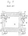
- Figures 9 and 10 show known types of active matrix liquid crystal display devices.
- One of a pair of substrates has gate buses 21 arranged transversely and source bases 23 perpendicular to the gate buses 21 . Every rectangular segment enclosed by the adjacent gate buses 21 and the source buses 23 have pixel electrodes 41 .
- a gate bus branch 22 branched off from the gate bus 21 has a TFT 31 as a switching element.
- the gate bus branch 22 includes a first section which functions as a gate electrode for the TFT 31 , and a second section which is narrower than the first section.
- a drain electrode 33 of the TFT 31 is electrically connected to the pixel electrodes 41 , and a source electrode 32 is connected to the source bus 23 .
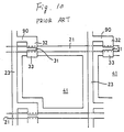
- Figure 10 shows another known example in which a source bus branch 90 branched from the source bus 23 overlaps the gate bus 21 , and a TFT 31 is formed on the overlapping part.
- a drain electrode 33 of the TFT 31 is electrically connected to the pixel electrodes 41
- a source electrode 32 is electrically connected to the source bus 23 through the source bus branch 90 .
- the "on fault” occurs owing to a defective switching element.
- the “off fault” occurs for a further two reasons; one is an electrical leakage through the switching element, and the other is an electrical leakage between the pixel electrodes and the buses. In either case, the voltage to be applied between the pixel electrodes and the counter electrode does not reach a required value. This causes faulty pixel electrodes to look like luminous points under the normal white mode (a mode in which the optical transmissibility reaches the maximum when the voltage applied to the liquid crystal is zero), and looks like a black point under the normal black mode (a mode in which the transmissibility is lowest when the voltage reaches zero).
- the active matrix display device of this invention which overcomes the above-discussed and numerous other disadvantages and deficiencies of the prior art, comprises a first insulating substrate and a second insulating substrate, a gate bus and a source bus arranged on the first insulating substrate in the form of a lattice, a pixel electrode arranged in a segment enclosed by the gate bus and the source bus, a switching element connected to the pixel electrode, the gate bus and the source bus, wherein the source bus comprises a projection extending toward the pixel electrode in such a manner as to be electrically disconnected from the pixel electrode, and the gate bus comprising a projection extending toward the pixel electrode, the source bus being overlaid on the gate bus projection with an insulating layer sandwiched therebetween, the gate bus projection being provided with an electroconductive member at the top thereof with an insulating layer sandwiched therebetween, the electroconductive member being electrically connected to the pixel electrode, and electrically disconnected from the source bus projection.
- an active matrix display device comprising a first insulating substrate and a second insulating substrate, a gate bus and a source bus arranged on the first insulating substrate in the form of a lattice, a pixel electrode arranged in a segment enclosed by the gate bus and the source bus, a switching element connected to the pixel electrode, an additive capacitance bus formed under the pixel electrode with an insulating layer sandwiched therebetween, wherein the source bus comprises a projection extending toward the pixel electrode in such a manner as to be electrically disconnected from the pixel electrode, and the additive capacitance bus comprises a projection extending toward the pixel electrode, the source bus being overlaid on the additive capacitance bus projection through an insulating layer, the source bus projection being provided with an electroconductive member at the top thereof with an insulating layer sandwiched therebetween, the electroconductive member being electrically connected to the pixel electrode and electrically disconnected from the source bus projection.
- an active matrix display device comprising a first insulating substrate and a second insulating substrate, a gate bus and a source bus arranged on the first insulating substrate in the form of a lattice, a pixel electrode arranged in a segment enclosed by the gate bus and the source bus, a switching element connected to the pixel electrode, a part of the pixel electrode being overlaid on an adjacent gate bus so as to form an additive Capacitance together with the gate bus with an insulating layer sandwiched therebetween, wherein the source bus is provided with a projection extending toward the pixel electrode in such a manner as to be electrically disconnected from the pixel electrode, and the gate bus being provided with a projection extending toward the pixel electrode, and the source bus being overlaid on the gate bus projection through an insulating layer, the gate bus projection being provided with an electroconductive member, the electroconductive member being electrically connected to the pixel electrode and electrically disconnected from the source bus projection.
- the switching element is a thin film transistor.
- an active matrix display device comprising a first insulating substrate and a second insulating substrate, a gate bus and a source bus arranged on the first insulating substrate in the form of a lattice, a pixel electrode arranged in a segment enclosed by the gate bus and the source bus, switching elements connected to the pixel electrode, gate bus and the source bus, wherein the source bus comprises a projection extending toward the pixel electrode in such a manner as to be electrically disconnected from the pixel electrode, and the gate bus comprises a projection extending toward the pixel electrode and whose top end reaches toward a forward end of the source bus projection, the switching element being formed toward the base end of the gate bus projection, a middle portion of the gate bus projection being overlaid on the source bus projection with an insulating layer sandwiched therebetween, the gate bus projection being provided with an electroconductive member at the top thereof through an insulating layer, the electroconductive member being electrically connected to the pixel electrode.
- an active matrix substrate comprising insulating substrates, pixel electrodes arranged in a matrix on the insulating substrates, the pixel electrodes being divided into split pixel electrodes, at least two source buses arranged in parallel between adjacent split pixel electrodes so as to transmit the same signals, the gate bus crossing the source bus and overlaying a part of the pixel electrode, gate bus branches branched from the gate bus, switching elements formed on the gate bus branches and connected to the adjacent split electrodes, connection lines electrically connecting the source buses, the connection lines crossing the gate bus branches with an insulation interposed therebetween.
- the switching element is a thin film transistor.
- an active matrix display device comprises a pair of insulating substrates, pixel electrodes arranged in a matrix on one of the substrates, gate buses and source buses crossing each other between the pixel electrodes, scanning branches branched from the gate buses, switching elements formed at top ends of the scanning branches and connected to the pixel electrodes, gate bus projections extending from the gate buses adjacent to those electrically connected to the pixel electrodes toward the corners of the pixel electrodes, source bus projections extending from the source buses adjacent to those electrically connected to the pixel electrodes toward the corners of the pixel electrodes, and electroconductive members overlaid on the ends of the gate bus projections through insulating layers and electrically connected to the pixel electrodes.
- the gate bus branches comprise a larger end portion and smaller portion other than the end portion.
- the invention described herein makes possible the objectives of (1) providing an active matrix display device which can detect and correct any faulty pixel electrodes by a simple procedure after all pixel electrodes are driven, (2) providing an active matrix display device which can be produced at low costs with a high manufacturing yield, and (3) providing an active matrix display device which can correct any faulty pixel electrodes without reducing the aperture ratio of the display panel.
- a display panel includes a lower transmissive insulating substrate 1 and an upper transmissive insulating substrate 2 disposed with a liquid crystal 18 sandwiched therebetween.
- the lower substrate 1 is provided with a plurality of gate buses 21 for scanning buses, a plurality of source buses 23 so that each rectangular section enclosed by the buses 21 and 23 has pixel electrodes 41 arranged in a matrix.
- the gate bus 21 has a branch line 22 which is provided with a TFT 31 at its top end.
- the TFT 31 functioning as a switching element, is connected to the pixel electrodes 41 .
- a gate bus 21b adjacent to a gate bus 21a connected to the pixel electrodes 41 is provided with a gate bus projection 43 extending inward from the corner of the pixel electrodes 41 .
- the projection 43 is provided with an electroconductive member 44 through a gate insulating film 13 ( Figures 2 and 3).
- the source bus 23 is also provided with a source bus projection 46 in correspondence with the corners of the pixel electrodes 41 .
- the source bus projection 46 overlays the gate bus projection 43 through the gate insulating film 13 .
- the gate bus 21 is formed on the transmissive insulating substrate 1 in a known manner.
- metal such as Ta, Ti, Al or Cr is deposited either as a single layer or as multi-layers on the transmissive insulating substrate, and then the layer or layers are patterned. Simultaneously, the gate bus branch 22 and the gate bus projection 43 are patterned.
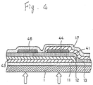
- the insulating substrates 1 are made of glass (in the drawings, one substrate along is shown for explanation convenience). It is possible to form an insulating film 11 of Ta2O5 or the line as a base coat as shown in Figure 4 .
- the gate insulating layer 13 is overlaid on the gate bus 21 (including the gate bus branch 22 and the gate bus projection 43 ).
- an SiN X film was formed to a thickness of 300 nm by a plasma CVD as the insulating layer 13 .
- a semiconductor layer 14 and an etching stopper layer 15 are successively formed on the gate insulating layer 13 by a plasma CVD method.
- the semiconductor layer 14 is made of amorphous silicon (a-Si) to a thickness of 30 nm, and the etching stopper layer 15 is made of SiN X to a thickness of 200 nm.
- the etching stopper layer 15 is patterned, and an n+ type a-Si layer 16 with phosphorus is deposited to a thickness of 80 nm by the plasma CVD method.
- the n+ type a-Si layer 16 is formed to enhance the ohmic contact between the semiconductor layer 14 and a source electrode 32 or a drain electrode 33 ( Figure 2) which will be deposited at a later stage.
- the n+ type a-Si layer 16 is patterned, and a source metal such as Ti, Al, Mo, or Cr is deposited by sputtering. In this example, Ti was used.
- the Ti layer is patterned so as to form the source electrode 32 and the drain electrode 33 .
- the finished thin film transistor (TFT) 31 is illustrated in Figure 2. At this stage, as shown in Figure 4, the source bus projection 46 and the electroconductive member 44 are simultaneously formed.
- the next step is to deposit a transmissive insulating substance for the pixel electrodes 41 .
- ITO indium tin oxide
- the pixel electrodes 41 which, as referred to above, is formed in the rectangular section enclosed by the gate bus 21 and the source bus 23 .
- the end portion of the pixel electrodes 41 is overlaid on an end portion of the drain electrode 33 of the TFT 31 .
- it is deposited on the electroconductive member 44 . In this way, energizing is effected through the pixel electrodes 41 , the drain electrode 33 of the TFT 31 and the electroconductive member 44 .
- the whole surface of the glass substrate 1 is covered with a protective layer 17 of SiN X .
- the protective layer 17 can be provided with a hole at a central part of the pixel electrodes 41 .
- An orientation layer 19 is formed on the protective layer 17 .
- the orientation layer 19 can be also provided with a hole at its center.
- a counter electrode 3 and an orientation layer 9 are formed on the glass substrate 2 .
- the reference numeral 18 denotes a liquid crystal sandwiched between the pair of insulating substrates 1 and 2 . In this way an active matrix display device is finished.
- a method of correcting a faulty pixel electrode will be described:
- the pixel electrodes 41 are driven by the TFT 31 unless the TFT 31 is in abnormal condition, and the pixel electrodes 41 in the segment enclosed by the gate bus 21 and the source bus 23 are put into regular operation. No problem arises on the display. If any abnormality occurs in the TFT 31 or a weak electric leak occurs between the source bus 23 and the pixel electrodes 41 , the pixel electrode becomes faulty, and the result appears on the display.
- This faulty pixel electrode is corrected in the following manner: First, the active matrix display device is driven so as to confirm the faulty pixel electrode.
- a segment 51 enclosed by dotted lines is irradiated with photo energy such as YAG laser beams so as to disperse the metal molecules in this segment 51 .
- photo energy such as YAG laser beams
- the gate bus 21 and the gate bus projection 43 are electrically disconnected from each other.
- a segment 52 enclosed by dotted lines is irradiated with laser beams so as to destroy the insulating layer 13 between the source bus projection 46 and the gate bus projection 43 .
- the two projections 46 and 43 are melted, thereby enabling them to electrically communicate with each other.
- the laser beams can be irradiated either from the side of the insulating substrate 1 on which the TFT 31 is formed or from the side of the substrate 2 on which the counter electrode is provided.
- the laser beams are irradiated from the side of the substrate 1 because of the coverage of the substrate 2 with a light shield metal.
- the directions of laser beams are indicated by white thick arrows.
- laser beams are irradiated upon the segment 53 , where the gate bus projection 43 and the electroconductive member 44 overlap each other. This irradiation destroys the insulating layer 13 , thereby enabling the gate bus projection 43 and the electroconductive member 44 to electrically communicate by fusing.
- the two irradiations of laser beams enable the upper and lower metal wirings to electrically communicate in the segments 52 and 53 , respectively. In this way the source bus 23 and the electroconductive members 44 , that is, the pixel electrodes 41 are short-circuited.
- the faulty pixel is lit at an average brightness achieved by all the normal pixels, thereby avoiding a faulty display.
- the gate bus branch 22 and the TFT 31 are covered with the protective layer 17 , thereby preventing a molten metal molecules from admixing with the liquid crystal 18 . This avoids the deterioration of the liquid crystal 18 .
- the irradiation of laser beams can be in various order for the segments 51 , 52 , and 53 as desired.
- the spots of irradiation need not be limited to the illustrated ones but any desired spots can be selected; for example, in the segments 52 and 53 any desired spots can be selected if they are within the overlapping portions of the upper and lower electroconductive layers.
- G n is a signal (voltage signal) from the (n)th gate bus 21
- S m is a signal from the (m)th source bus 23
- P n,m is a signal given to pixel electrodes 41 present at the junction of the (n)th gate bus 21 and the (m)th source bus 23 .
- the reference signal Gn+1 denotes a signal applied to the ( Gn+1 )th gate bus 21 .
- This signal Gn+1 is selected when the period of time Ton for selecting the gate bus 21 expires.
- the signal -V1 is written in the source bus 23 ( Figure 5(c)).
- the signals applied to the gate bus 21 are consecutively delayed in the order of the line number, and the non-selection period of time continues over the period of time Toff until the (n)th gate bus 21 is selected.
- the non-selective period of time signals to be written in the pixel electrodes 41 are continuously applied to the source bus 23 .
- the pixel electrodes 41 that are in normal condition are charged in response to the signal Sm input from the source bus 23 when the gate signal Gn is selected, thereby changing the molecular arrangement of the liquid crystal 18 at an electric potential between the counter electrode 3 on the substrate 2 and the liquid crystal 18 .
- the signals Sm input to the source bus 23 during the non-selection period of time Toff do not contribute to the display at all.
- the pixel electrodes 41 and the source bus 23 are short-circuited by the irradiation of laser beams, the pixel electrodes 41 are subjected to electrical charging or discharging in response to all the signals Sm input from the source bus 23 irrespective of the selection and non-selection of the gate bus 21 , wherein the signal is indicated by P'n,m in Figure 5(e).
- the pixel electrode 41 that was corrected by the irradiation of laser beams receives the signal Sm directly from the source bus 23 during the non-selection period of time Toff .
- the voltage is applied to the liquid crystal 18 at its effective value.
- the effective value of the signal P'n,m cannot be V0
- the effective value of the signal voltage P'n,m is an average value of all the pixel electrodes 41 connected to the (m)th source bus 23 .
- the display device is lit at an average brightness of the pixel electrodes 41 arranged along the (m)th source bus 23 .
- Each pixel electrode is lit at such a sufficient brightness so as to maintain the quality of representation on the screen.
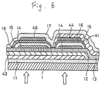
- Figure 6 shows a modified version which includes a semiconductor layer 14 , an etching stopper layer 15 and a contact layer 16 between the gate insulating layer 13 and an electroconductive member 44 , and between the gate insulating layer 13 and the source bus projection 46 , respectively.
- These layers 14 to 16 are provided to electrically disconnect the upper electroconductive layers from the lower electroconductive layers, and vice versa.
- the semiconductor layer 14 and the etching stopper 15 , or the contact layer 16 alone can be inserted.
- FIG. 7 shows a further modified version in which each pixel electrode 41 has an additive capacitance 42 which is constituted by an additive capacitance bus 24 arranged in parallel with the gate bus 21 and the gate insulating layer 13 . More specifically, the additive capacitance bus 24 and the pixel electrodes 41 partly overlap one another, and the additive capacitance 42 is formed on the overlapping portion as shown by hatching in Figure 7.
- the additive capacitance bus 24 is formed by depositing the same metal as that of the gate bus 21 , and patterning simultaneously when the gate bus 21 is patterned.
- This example shown in Figure 7 is constructed so that the same signal is input to the additive capacitance bus 24 as the counter electrode 3 .
- the additive capacitance 42 is in parallel with the capacitance of the liquid crystal 18 .
- the additive capacitance 42 maintains the charge of the pixel electrodes 41 , thereby enhancing the performance of the display device.
- the faulty pixel can be corrected in the same manner as described above.
- Figure 8 shows another modified version in which the additive capacitance 42 is formed by the adjacent gate bus 21 . More specifically, the additive capacitance bus 24 is integrated with the gate bus 21 , and the additive capacitance 42 is formed on an overlapping portion of the pixel electrodes 41 and the gate bus 21 through the gate insulating layer 13 as shown by hatching in Figure 8.
- the adjacent gate bus 21 is not selected, the same signal is input to the gate bus 21 as that applied to the counter electrode 3 on the glass substrate 2 .
- This gate bus 21 is used as the additive capacitance bus 24 . This decreases the light shading area, thereby avoiding a dark image picture. Thus the display performance is enhanced.
- the TFTs are used as switching elements, but an MIM element, a MOS transistor, a diode or a varistor can be used.
- the TFT is not limited to the illustrated structure but can be variously modified; for example, a source bus can be placed as a lower layer, and a gate bus can be placed as an upper layer.
- An active matrix substrate suitable for use in the active matrix display device will be described:
- An insulating substrate 100 is provided with pixel electrodes 104 arranged in a matrix, each pixel electrode being divided into two electrodes 104a and 104b , which will be hereinafter referred to as split electrodes, two source buses 102a and 102b , the source buses 102a and 102b passing in parallel between adjacent split electrodes 104a and 104b so as to transmit the same signal, and a gate bus 101 crossing at right angles to the source buses 102a and 102b , the gate bus 101 and portions of the pixel electrodes 104 overlapping one another, a gate bus branch 111 , thin film transistors (TFTs) 103 and a connection line 102c connecting the two source buses 102a and 102b .
- the connection line 102c crosses the gate bus branch 111 with an insulation interposed therebetween.
- the gate buses 101 function as scanning lines, the source buses 102a and 102b as signal lines, the gate bus branches 111 as scanning branches, and the TFT 103 as a switching element.
- the substrate is fabricated as follows: A Ta layer is formed on the insulating substrate 110 by sputtering, and patterned to form the gate bus 101 and the gate bus branch 111 .
- Ti, Al or Cr can be used instead of Ta.
- the layer can be single or multiple. It is possible to cover the whole surface of the substrate 110 with an insulating layer of Ta2O5.
- the surfaces of gate bus 101 and the gate bus branch 111 can be anodized so as to form an anodized layer. Other parts of the process are the same as those described above.
- one pixel electrode is split into two parts by the two source buses 102a and 102b which transmit the same image signal, but the substrate 110 can be provided with three source buses or more which transmit the same signal.
- the three source buses must be mutually connected by use of two or more connection lines. It is not always necessary to provide each pixel electrode with the connecting line 102c but it is sufficient if the source buses 102a and 102b are connected by at least one connecting means.
- the gate buses 101 constitute additive capacitance electrodes, thereby reducing the area of the pixel electrodes 104 as a whole.
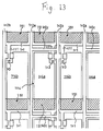
- FIG 13 shows a modification to the substrate shown in Figures 11 and 12.
- Two TFTs 103 connected to the split electrodes 104a and 104b are connected to the same source buses 102a or 102b .
- the other structure is the same as that of Figure 11.
- TFTs 103 are not connected to the source bus 102a that functions as a bypass.
- a faulty pixel can be detected after all the pixel electrodes are driven.
- the detection can be easily done by irradiating the display panel with laser beams from outside the insulating substrates. As a result, the manufacturing yield is increased.
Landscapes
- Physics & Mathematics (AREA)
- Nonlinear Science (AREA)
- Engineering & Computer Science (AREA)
- Microelectronics & Electronic Packaging (AREA)
- Mathematical Physics (AREA)
- Chemical & Material Sciences (AREA)
- Crystallography & Structural Chemistry (AREA)
- General Physics & Mathematics (AREA)
- Optics & Photonics (AREA)
- Liquid Crystal (AREA)
- Devices For Indicating Variable Information By Combining Individual Elements (AREA)
Abstract
Description
- The present invention relates generally to an active matrix display device, and more particularly to an active matrix display device in which switching elements such as thin film transistors apply drive signals to pixel electrodes arranged in a matrix so as to achieve a high density display.
- In the known liquid crystal display devices, EL displays devices, plasma display devices, etc. the pixel electrodes arranged in a matrix are selectively driven so as to represent a pattern on a screen. The pixel electrodes are individually provided with switching elements through which the pixel electrodes are selectively driven. This is commonly called an active matrix driving system. The switching elements are made of a thin film transistor (TFT), a metal-insulator metal (MIM), a MOS transistor, a diode and a varistor. A voltage applied between the individual pixel electrodes and counter electrodes is switched on, and a liquid crystal, an EL light emitting medium, a plasma light emitting device make the display medium optically modulated. The optical modulation is observed as displayed patterns by the naked eye. The active matrix display device is suitable for display in high contrast, and finds application in liquid crystal television, word processors, and terminal display units of computers.
- Figures 9 and 10 show known types of active matrix liquid crystal display devices. One of a pair of substrates has
gate buses 21 arranged transversely andsource bases 23 perpendicular to thegate buses 21. Every rectangular segment enclosed by theadjacent gate buses 21 and thesource buses 23 havepixel electrodes 41. - A
gate bus branch 22 branched off from thegate bus 21 has a TFT 31 as a switching element. Thegate bus branch 22 includes a first section which functions as a gate electrode for theTFT 31, and a second section which is narrower than the first section. Adrain electrode 33 of theTFT 31 is electrically connected to thepixel electrodes 41, and asource electrode 32 is connected to thesource bus 23. - Figure 10 shows another known example in which a
source bus branch 90 branched from thesource bus 23 overlaps thegate bus 21, and a TFT 31 is formed on the overlapping part. Adrain electrode 33 of the TFT 31 is electrically connected to thepixel electrodes 41, and asource electrode 32 is electrically connected to thesource bus 23 through thesource bus branch 90. - Under this arrangement of the known active matrix display device a problem arises, for example, if any switching element malfunctions, the pixel electrodes connected thereto receives no signal. This appears as devoid of pixel electrode. The absence of pixel electrode spoils the representation of the display device. This results in a lower manufacturing yield.
- Such faulty or defective pixel electrodes occurs for the following two reasons:
- (1) The pixel electrodes are not fully charged until the switching elements are selected by a scanning signal (signals from the gate bus) (hereinafter referred to as "on fault"), and
- (2) An electric leakage occurs through the charged pixel electrodes before the switching elements are selected (hereinafter referred to "off fault").
- The "on fault" occurs owing to a defective switching element. The "off fault" occurs for a further two reasons; one is an electrical leakage through the switching element, and the other is an electrical leakage between the pixel electrodes and the buses. In either case, the voltage to be applied between the pixel electrodes and the counter electrode does not reach a required value. This causes faulty pixel electrodes to look like luminous points under the normal white mode (a mode in which the optical transmissibility reaches the maximum when the voltage applied to the liquid crystal is zero), and looks like a black point under the normal black mode (a mode in which the transmissibility is lowest when the voltage reaches zero).
- If these faults are found during the fabrication of a substrate in which the switching elements are arranged, they can be trimmed by laser. In fact, however, it is almost impossible to find a single faulty one in a great number of pixel electrodes. The mass production of substrates cannot be carried out without increasing costs and prolonging the time. It is completely impossible to do so in a large size display panel having 100,000 to 500,000 pixel electrodes.
- It is possible to visually observe a faulty pixel electrode by overlaying a counter substrate on a substrate in question, injecting liquid crystal therebetween and applying an inspection signal to the source bus. This method requires a correction in which the source bus and the pixel electrodes are short-circuited so as to effect the charge and discharge of the pixel electrodes by a signal voltage irrespective of whether the source bus was selected or not. In the example shown in Figures 9 and 10, it is inherently difficult to do such a correction because of the arrangement of the
source bus 23 and thepixel electrodes 41. After all, the display device containing the faulty pixel electrodes has to be discarded even if other components and elements are in good condition. This is wasteful, and increases the production cost. This accounts for the decreased manufacturing yield. - The active matrix display device of this invention, which overcomes the above-discussed and numerous other disadvantages and deficiencies of the prior art, comprises a first insulating substrate and a second insulating substrate, a gate bus and a source bus arranged on the first insulating substrate in the form of a lattice, a pixel electrode arranged in a segment enclosed by the gate bus and the source bus, a switching element connected to the pixel electrode, the gate bus and the source bus, wherein the source bus comprises a projection extending toward the pixel electrode in such a manner as to be electrically disconnected from the pixel electrode, and the gate bus comprising a projection extending toward the pixel electrode, the source bus being overlaid on the gate bus projection with an insulating layer sandwiched therebetween, the gate bus projection being provided with an electroconductive member at the top thereof with an insulating layer sandwiched therebetween, the electroconductive member being electrically connected to the pixel electrode, and electrically disconnected from the source bus projection.
- Alternatively, an active matrix display device comprising a first insulating substrate and a second insulating substrate, a gate bus and a source bus arranged on the first insulating substrate in the form of a lattice, a pixel electrode arranged in a segment enclosed by the gate bus and the source bus, a switching element connected to the pixel electrode, an additive capacitance bus formed under the pixel electrode with an insulating layer sandwiched therebetween, wherein the source bus comprises a projection extending toward the pixel electrode in such a manner as to be electrically disconnected from the pixel electrode, and the additive capacitance bus comprises a projection extending toward the pixel electrode, the source bus being overlaid on the additive capacitance bus projection through an insulating layer, the source bus projection being provided with an electroconductive member at the top thereof with an insulating layer sandwiched therebetween, the electroconductive member being electrically connected to the pixel electrode and electrically disconnected from the source bus projection.
- Alternatively, an active matrix display device comprising a first insulating substrate and a second insulating substrate, a gate bus and a source bus arranged on the first insulating substrate in the form of a lattice, a pixel electrode arranged in a segment enclosed by the gate bus and the source bus, a switching element connected to the pixel electrode, a part of the pixel electrode being overlaid on an adjacent gate bus so as to form an additive Capacitance together with the gate bus with an insulating layer sandwiched therebetween, wherein the source bus is provided with a projection extending toward the pixel electrode in such a manner as to be electrically disconnected from the pixel electrode, and the gate bus being provided with a projection extending toward the pixel electrode, and the source bus being overlaid on the gate bus projection through an insulating layer, the gate bus projection being provided with an electroconductive member, the electroconductive member being electrically connected to the pixel electrode and electrically disconnected from the source bus projection.
- In a preferred embodiment, the switching element is a thin film transistor.
- Alternatively, an active matrix display device comprising a first insulating substrate and a second insulating substrate, a gate bus and a source bus arranged on the first insulating substrate in the form of a lattice, a pixel electrode arranged in a segment enclosed by the gate bus and the source bus, switching elements connected to the pixel electrode, gate bus and the source bus, wherein the source bus comprises a projection extending toward the pixel electrode in such a manner as to be electrically disconnected from the pixel electrode, and the gate bus comprises a projection extending toward the pixel electrode and whose top end reaches toward a forward end of the source bus projection, the switching element being formed toward the base end of the gate bus projection, a middle portion of the gate bus projection being overlaid on the source bus projection with an insulating layer sandwiched therebetween, the gate bus projection being provided with an electroconductive member at the top thereof through an insulating layer, the electroconductive member being electrically connected to the pixel electrode.
- Alternatively, an active matrix substrate comprising insulating substrates, pixel electrodes arranged in a matrix on the insulating substrates, the pixel electrodes being divided into split pixel electrodes, at least two source buses arranged in parallel between adjacent split pixel electrodes so as to transmit the same signals, the gate bus crossing the source bus and overlaying a part of the pixel electrode, gate bus branches branched from the gate bus, switching elements formed on the gate bus branches and connected to the adjacent split electrodes, connection lines electrically connecting the source buses, the connection lines crossing the gate bus branches with an insulation interposed therebetween.
- In a preferred embodiment, the switching element is a thin film transistor.
- Alternatively, an active matrix display device comprises a pair of insulating substrates, pixel electrodes arranged in a matrix on one of the substrates, gate buses and source buses crossing each other between the pixel electrodes, scanning branches branched from the gate buses, switching elements formed at top ends of the scanning branches and connected to the pixel electrodes, gate bus projections extending from the gate buses adjacent to those electrically connected to the pixel electrodes toward the corners of the pixel electrodes, source bus projections extending from the source buses adjacent to those electrically connected to the pixel electrodes toward the corners of the pixel electrodes, and electroconductive members overlaid on the ends of the gate bus projections through insulating layers and electrically connected to the pixel electrodes.
- In a preferred embodiment, the gate bus branches comprise a larger end portion and smaller portion other than the end portion.
- Thus, the invention described herein makes possible the objectives of (1) providing an active matrix display device which can detect and correct any faulty pixel electrodes by a simple procedure after all pixel electrodes are driven, (2) providing an active matrix display device which can be produced at low costs with a high manufacturing yield, and (3) providing an active matrix display device which can correct any faulty pixel electrodes without reducing the aperture ratio of the display panel.
- This invention may be better understood and its numerous objects and advantages will become apparent to those skilled in the art by reference to the accompanying drawings as follows:
- Figure 1 is a plan view showing an active matrix display device according to the present invention;
- Figure 2 is a cross-sectional view taken along the line A-A in Figure 1;
- Figure 3 is a fragmentary plan view on an enlarged scale showing the active matrix display device shown in Figure 1;
- Figure 4 is a cross-sectional view taken along the line C-C in Figure 3;
- Figure 5 is a timing chart showing the signals input to the gate bus, source bus and pixel electrodes;
- Figure 6 is a cross-sectional view showing a modified version of the present invention;
- Figure 7 is a plan view showing another example of the present invention;
- Figure 8 is a plan view showing another example of the present invention;
- Figure 9 is a plan view showing an example of a prior art active matrix display device;
- Figure 10 is a plan view showing another example of a prior art active matrix display device;
- Figure 11 is a plan view showing a substrate used in an active matrix display according to the present invention;
- Figure 12 is a cross-sectional view taken along the line II-II in Figure 11; and
- Figure 13 is a plan view showing other example of the substrate.
- Referring to Figures 1 to 4, a display panel includes a lower
transmissive insulating substrate 1 and an uppertransmissive insulating substrate 2 disposed with aliquid crystal 18 sandwiched therebetween. Thelower substrate 1 is provided with a plurality ofgate buses 21 for scanning buses, a plurality ofsource buses 23 so that each rectangular section enclosed by thebuses pixel electrodes 41 arranged in a matrix. Thegate bus 21 has abranch line 22 which is provided with aTFT 31 at its top end. TheTFT 31, functioning as a switching element, is connected to thepixel electrodes 41. In Figure 1, agate bus 21b adjacent to agate bus 21a connected to thepixel electrodes 41 is provided with agate bus projection 43 extending inward from the corner of thepixel electrodes 41. Theprojection 43 is provided with anelectroconductive member 44 through a gate insulating film 13 (Figures 2 and 3). - The
source bus 23 is also provided with asource bus projection 46 in correspondence with the corners of thepixel electrodes 41. Thesource bus projection 46 overlays thegate bus projection 43 through thegate insulating film 13. - A process of fabricating the display panel will be described in detail:
- The
gate bus 21 is formed on the transmissive insulatingsubstrate 1 in a known manner. For example, metal such as Ta, Ti, Al or Cr is deposited either as a single layer or as multi-layers on the transmissive insulating substrate, and then the layer or layers are patterned. Simultaneously, thegate bus branch 22 and thegate bus projection 43 are patterned. In this example, the insulatingsubstrates 1 are made of glass (in the drawings, one substrate along is shown for explanation convenience). It is possible to form an insulatingfilm 11 of Ta₂O₅ or the line as a base coat as shown in Figure 4. - Then, the
gate insulating layer 13 is overlaid on the gate bus 21 (including thegate bus branch 22 and the gate bus projection 43). In this example, an SiNX film was formed to a thickness of 300 nm by a plasma CVD as the insulatinglayer 13. Alternatively, it is possible to form an oxidized layer of Ta₂O₅ by anodizing thegate bus 21 prior to the formation of thegate insulating layer 13. - A
semiconductor layer 14 and anetching stopper layer 15 are successively formed on thegate insulating layer 13 by a plasma CVD method. Thesemiconductor layer 14 is made of amorphous silicon (a-Si) to a thickness of 30 nm, and theetching stopper layer 15 is made of SiNX to a thickness of 200 nm. Theetching stopper layer 15 is patterned, and an n⁺type a-Si layer 16 with phosphorus is deposited to a thickness of 80 nm by the plasma CVD method. The n⁺type a-Si layer 16 is formed to enhance the ohmic contact between thesemiconductor layer 14 and asource electrode 32 or a drain electrode 33 (Figure 2) which will be deposited at a later stage. - Then, the n⁺
type a-Si layer 16 is patterned, and a source metal such as Ti, Al, Mo, or Cr is deposited by sputtering. In this example, Ti was used. The Ti layer is patterned so as to form thesource electrode 32 and thedrain electrode 33. The finished thin film transistor (TFT) 31 is illustrated in Figure 2. At this stage, as shown in Figure 4, thesource bus projection 46 and theelectroconductive member 44 are simultaneously formed. - The next step is to deposit a transmissive insulating substance for the
pixel electrodes 41. In this example, ITO (indium tin oxide) was deposited by sputtering and patterned so as to form thepixel electrodes 41, which, as referred to above, is formed in the rectangular section enclosed by thegate bus 21 and thesource bus 23. As shown in Figure 2, the end portion of thepixel electrodes 41 is overlaid on an end portion of thedrain electrode 33 of theTFT 31. More specifically, as shown in Figure 3, it is deposited on theelectroconductive member 44. In this way, energizing is effected through thepixel electrodes 41, thedrain electrode 33 of theTFT 31 and theelectroconductive member 44. - The whole surface of the
glass substrate 1 is covered with aprotective layer 17 of SiNX. Theprotective layer 17 can be provided with a hole at a central part of thepixel electrodes 41. Anorientation layer 19 is formed on theprotective layer 17. Theorientation layer 19 can be also provided with a hole at its center. As shown in Figure 2, a counter electrode 3 and an orientation layer 9 are formed on theglass substrate 2. Thereference numeral 18 denotes a liquid crystal sandwiched between the pair of insulatingsubstrates - A method of correcting a faulty pixel electrode will be described:
Thepixel electrodes 41 are driven by theTFT 31 unless theTFT 31 is in abnormal condition, and thepixel electrodes 41 in the segment enclosed by thegate bus 21 and thesource bus 23 are put into regular operation. No problem arises on the display. If any abnormality occurs in theTFT 31 or a weak electric leak occurs between thesource bus 23 and thepixel electrodes 41, the pixel electrode becomes faulty, and the result appears on the display. This faulty pixel electrode is corrected in the following manner:
First, the active matrix display device is driven so as to confirm the faulty pixel electrode. As shown in Figure 3, if any abnormality is discovered, asegment 51 enclosed by dotted lines is irradiated with photo energy such as YAG laser beams so as to disperse the metal molecules in thissegment 51. In this way thegate bus 21 and thegate bus projection 43 are electrically disconnected from each other. Then asegment 52 enclosed by dotted lines is irradiated with laser beams so as to destroy the insulatinglayer 13 between thesource bus projection 46 and thegate bus projection 43. Thus the twoprojections - The laser beams can be irradiated either from the side of the insulating
substrate 1 on which theTFT 31 is formed or from the side of thesubstrate 2 on which the counter electrode is provided. In this example, the laser beams are irradiated from the side of thesubstrate 1 because of the coverage of thesubstrate 2 with a light shield metal. In Figure 4, the directions of laser beams are indicated by white thick arrows. - Second, laser beams are irradiated upon the
segment 53, where thegate bus projection 43 and theelectroconductive member 44 overlap each other. This irradiation destroys the insulatinglayer 13, thereby enabling thegate bus projection 43 and theelectroconductive member 44 to electrically communicate by fusing. The two irradiations of laser beams enable the upper and lower metal wirings to electrically communicate in thesegments source bus 23 and theelectroconductive members 44, that is, thepixel electrodes 41 are short-circuited. - Because of the short-circuit the faulty pixel is lit at an average brightness achieved by all the normal pixels, thereby avoiding a faulty display.
- The
gate bus branch 22 and theTFT 31 are covered with theprotective layer 17, thereby preventing a molten metal molecules from admixing with theliquid crystal 18. This avoids the deterioration of theliquid crystal 18. - The irradiation of laser beams can be in various order for the
segments segments - Referring now to Figure 5, explanation will be given as to how the TFT is operated when the
pixel electrodes 41 and thesource bus 23 are short-circuited:
In Figure 5, G n is a signal (voltage signal) from the (n)th gate bus 21, S m is a signal from the (m)th source bus 23, P n,m is a signal given topixel electrodes 41 present at the junction of the (n)th gate bus 21 and the (m)th source bus 23. - As shown in Figure 5(a), when the potential of the signal from the
gate bus 21 is Vgh (at a high level), theTFT 31 is selected, and when it is Vgl (at a low level), theTFT 31 is not selected. As shown in Figure 5(c), when theTFT 31 is selected, a pulse signal V0 is charged in thepixel electrodes 41. When thepixel electrode 41 is in a normal operation, the signal V0 is held for a period of time Toff when theTFT 31 is not selected, and a signal -V0 is written in thesource bus 23 at a point of time Ton when theTFT 31 is selected. - In Figure 5(b) the reference signal Gn+1 denotes a signal applied to the (Gn+1)
th gate bus 21. This signal Gn+1 is selected when the period of time Ton for selecting thegate bus 21 expires. At this time the signal -V1 is written in the source bus 23 (Figure 5(c)). As is evident from Figures 5(a) and 5(b), the signals applied to thegate bus 21 are consecutively delayed in the order of the line number, and the non-selection period of time continues over the period of time Toff until the (n)th gate bus 21 is selected. During the non-selective period of time signals to be written in thepixel electrodes 41 are continuously applied to thesource bus 23. - As shown in Figure 5(d), the
pixel electrodes 41 that are in normal condition are charged in response to the signal Sm input from thesource bus 23 when the gate signal Gn is selected, thereby changing the molecular arrangement of theliquid crystal 18 at an electric potential between the counter electrode 3 on thesubstrate 2 and theliquid crystal 18. In this way the display is effected. At this stage, the signals Sm input to thesource bus 23 during the non-selection period of time Toff do not contribute to the display at all. - When the
pixel electrodes 41 and thesource bus 23 are short-circuited by the irradiation of laser beams, thepixel electrodes 41 are subjected to electrical charging or discharging in response to all the signals Sm input from thesource bus 23 irrespective of the selection and non-selection of thegate bus 21, wherein the signal is indicated by P'n,m in Figure 5(e). Thepixel electrode 41 that was corrected by the irradiation of laser beams receives the signal Sm directly from thesource bus 23 during the non-selection period of time Toff. Thus, the voltage is applied to theliquid crystal 18 at its effective value. Except when the signals Sm applied to thesource bus 23 becomes V0, the effective value of the signal P'n,m cannot be V0, but the effective value of the signal voltage P'n,m is an average value of all thepixel electrodes 41 connected to the (m)th source bus 23. This means that the display device is lit at an average brightness of thepixel electrodes 41 arranged along the (m)th source bus 23. Each pixel electrode is lit at such a sufficient brightness so as to maintain the quality of representation on the screen. - Figure 6 shows a modified version which includes a
semiconductor layer 14, anetching stopper layer 15 and acontact layer 16 between thegate insulating layer 13 and anelectroconductive member 44, and between thegate insulating layer 13 and thesource bus projection 46, respectively. Theselayers 14 to 16 are provided to electrically disconnect the upper electroconductive layers from the lower electroconductive layers, and vice versa. Instead of theselayers 14 to 16, thesemiconductor layer 14 and theetching stopper 15, or thecontact layer 16 alone can be inserted. - Figure 7 shows a further modified version in which each
pixel electrode 41 has anadditive capacitance 42 which is constituted by anadditive capacitance bus 24 arranged in parallel with thegate bus 21 and thegate insulating layer 13. More specifically, theadditive capacitance bus 24 and thepixel electrodes 41 partly overlap one another, and theadditive capacitance 42 is formed on the overlapping portion as shown by hatching in Figure 7. Theadditive capacitance bus 24 is formed by depositing the same metal as that of thegate bus 21, and patterning simultaneously when thegate bus 21 is patterned. - This example shown in Figure 7 is constructed so that the same signal is input to the
additive capacitance bus 24 as the counter electrode 3. As a circuit theadditive capacitance 42 is in parallel with the capacitance of theliquid crystal 18. Theadditive capacitance 42 maintains the charge of thepixel electrodes 41, thereby enhancing the performance of the display device. In this example, the faulty pixel can be corrected in the same manner as described above. - Figure 8 shows another modified version in which the
additive capacitance 42 is formed by theadjacent gate bus 21. More specifically, theadditive capacitance bus 24 is integrated with thegate bus 21, and theadditive capacitance 42 is formed on an overlapping portion of thepixel electrodes 41 and thegate bus 21 through thegate insulating layer 13 as shown by hatching in Figure 8. When theadjacent gate bus 21 is not selected, the same signal is input to thegate bus 21 as that applied to the counter electrode 3 on theglass substrate 2. Thisgate bus 21 is used as theadditive capacitance bus 24. This decreases the light shading area, thereby avoiding a dark image picture. Thus the display performance is enhanced. - In the illustrated embodiments the TFTs are used as switching elements, but an MIM element, a MOS transistor, a diode or a varistor can be used. The TFT is not limited to the illustrated structure but can be variously modified; for example, a source bus can be placed as a lower layer, and a gate bus can be placed as an upper layer.
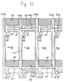
- Referring to Figures 11 and 12, an active matrix substrate suitable for use in the active matrix display device will be described:
An insulating substrate 100 is provided withpixel electrodes 104 arranged in a matrix, each pixel electrode being divided into twoelectrodes source buses source buses adjacent split electrodes gate bus 101 crossing at right angles to thesource buses gate bus 101 and portions of thepixel electrodes 104 overlapping one another, agate bus branch 111, thin film transistors (TFTs) 103 and aconnection line 102c connecting the twosource buses connection line 102c crosses thegate bus branch 111 with an insulation interposed therebetween. - The
gate buses 101 function as scanning lines, thesource buses gate bus branches 111 as scanning branches, and theTFT 103 as a switching element. - The substrate is fabricated as follows:
A Ta layer is formed on the insulatingsubstrate 110 by sputtering, and patterned to form thegate bus 101 and thegate bus branch 111. As referred to above, Ti, Al or Cr can be used instead of Ta. The layer can be single or multiple. It is possible to cover the whole surface of thesubstrate 110 with an insulating layer of Ta₂O₅. The surfaces ofgate bus 101 and thegate bus branch 111 can be anodized so as to form an anodized layer. Other parts of the process are the same as those described above. In the illustrated embodiment, one pixel electrode is split into two parts by the twosource buses substrate 110 can be provided with three source buses or more which transmit the same signal. In this case, the three source buses must be mutually connected by use of two or more connection lines. It is not always necessary to provide each pixel electrode with the connectingline 102c but it is sufficient if thesource buses - If any of the
source bus lines 102c so as to enable the image signal to reach beyond the broken point, thereby avoiding the occurrence of troubles due to line breakage. Thegate buses 101 constitute additive capacitance electrodes, thereby reducing the area of thepixel electrodes 104 as a whole. - Figure 13 shows a modification to the substrate shown in Figures 11 and 12. Two
TFTs 103 connected to thesplit electrodes same source buses TFTs 103 are not connected to thesource bus 102a that functions as a bypass. - As is evident from the foregoing description, according to the present invention a faulty pixel can be detected after all the pixel electrodes are driven. In addition, the detection can be easily done by irradiating the display panel with laser beams from outside the insulating substrates. As a result, the manufacturing yield is increased.
- It is understood that various other modifications will be apparent to and can be readily made by those skilled in the art without departing from the scope and spirit of this invention. Accordingly, it is not intended that the scope of the claims appended hereto be limited to the description as set forth herein, but rather that the claims be construed as encompassing all the features of patentable novelty that reside in the present invention, including all features that would be treated as equivalents thereof by those skilled in the art to which this invention pertains.
Claims (14)
- An active matrix display device comprising a first insulating substrate and a second insulating substrate, a gate bus and a source bus arranged on the first insulating substrate in the form of a lattice, a pixel electrode arranged in a segment enclosed by the gate bus and the source bus, a switching element connected to the pixel electrode, the gate bus and the source bus, wherein the source bus comprises a projection extending toward the pixel electrode in such a manner as to be electrically disconnected from the pixel electrode, and the gate bus comprising a projection extending toward the pixel electrode, the source bus being overlaid on the gate bus projection with an insulating layer sandwiched therebetween, the gate bus projection being provided with an electroconductive member at the top thereof with an insulating layer sandwiched therebetween, the electroconductive member being electrically connected to the pixel electrode, and electrically disconnected from the source bus projection.
- An active matrix display device comprising a first insulating substrate and a second insulating substrate, a gate bus and a source bus arranged on the first insulating substrate in the form of a lattice, a pixel electrode arranged in a segment enclosed by the gate bus and the source bus, a switching element connected to the pixel electrode, an additive capacitance bus formed under the pixel electrode with an insulating layer sandwiched therebetween, wherein the source bus comprises a projection extending toward the pixel electrode in such a manner as to be electrically disconnected from the pixel electrode, and the additive capacitance bus comprises a projection extending toward the pixel electrode, the source bus being overlaid on the additive capacitance bus projection through an insulating layer, the source bus projection being provided with an electroconductive member at the top thereof with an insulating layer sandwiched therebetween, the electroconductive member being electrically connected to the pixel electrode and electrically disconnected from the source bus projection.
- An active matrix display device comprising a first insulating substrate and a second insulating substrate, a gate bus and a source bus arranged on the first insulating substrate in the form of a lattice, a pixel electrode arranged in a segment enclosed by the gate bus and the source bus, a switching element connected to the pixel electrode, a part of the pixel electrode being overlaid on an adjacent gate bus so as to form an additive capacitance together with the gate bus with an insulating layer sandwiched therebetween, wherein the source bus is provided with a projection extending toward the pixel electrode in such a manner as to be electrically disconnected from the pixel electrode, and the gate bus being provided with a projection extending toward the pixel electrode, and the source bus being overlaid on the gate bus projection through an insulating layer, the gate bus projection being provided with an electroconductive member, the electroconductive member being electrically connected to the pixel electrode and electrically disconnected from the source bus projection.
- An active matrix display device as defined in any of claims 1 or 3, wherein the switching element is a thin film transistor.
- An active matrix display device comprising a first insulating substrate and a second insulating substrate, a gate bus and a source bus arranged on the first insulating substrate in the form of a lattice, a pixel electrode arranged in a segment enclosed by the gate bus and the source bus, switching elements connected to the pixel electrode, gate bus and the source bus, wherein the source bus comprises a projection extending toward the pixel electrode in such a manner as to be electrically disconnected from the pixel electrode, and the gate bus comprises a projection extending toward the pixel electrode and whose top end reaches toward a forward end of the source bus projection, the switching element being formed toward the base end of the gate bus projection, a middle portion of the gate bus projection being overlaid on the source bus projection with an insulating layer sandwiched therebetween, the gate bus projection being provided with an electroconductive member at the top thereof through an insulating layer, the electroconductive member being electrically connected to the pixel electrode.
- An active matrix substrate comprising insulating substrates, pixel electrodes arranged in a matrix on the insulating substrates, the pixel electrodes being divided into split pixel electrodes, at least two source buses arranged in parallel between adjacent split pixel electrodes so as to transmit the same signals, the gate bus crossing the source bus and overlaying a part of the pixel electrode, gate bus branches branched from the gate bus, switching elements formed on the gate bus branches and connected to the adjacent split electrodes, connection lines electrically connecting the source buses, the connection lines crossing the gate bus branches with an insulation interposed therebetween.
- An active matrix display device as defined in claim 6, wherein the switching element is a thin film transistor.
- An active matrix display device comprising a pair of insulating substrates, pixel electrodes arranged in a matrix on one of the substrates, gate buses and source buses crossing each other between the pixel electrodes, gate bus branches branched from the gate buses, switching elements formed at top ends of the scanning branches and connected to the pixel electrodes, gate bus projections extending from the gate buses adjacent to those electrically connected to the pixel electrodes toward the corners of the pixel electrodes, source bus projections extending from the source buses adjacent to those electrically connected to the pixel electrodes toward the corners of the pixel electrodes, and electroconductive members overlaid on the ends of the gate bus projections through insulating layers and electrically connected to the pixel electrodes.
- An active matrix display device as defined in claim 8, wherein the gate bus branches comprise a larger end portion and smaller portion other than the end portion.
- An active matrix display device with pixel-controlling switching elements formed on an insulating substrate on which also are formed pixel electrodes and a lattice arrangement of first source bus lines extending in a column direction and second lines extending in a row direction transverse the source lines, wherein for each pixel electrode there are provided first and second projections respectively from a said first and second line, one of said projections overlapping the other, and the second projection having a portion lying beneath the pixel electrode, whereby connections can be made between the first and second projections and between the second projection and the pixel electrode so as to short the pixel electrode to the first line.
- An active matrix display device according to claim 10 wherein said second lines are gate bus lines.
- An active matrix display device according to claim 11 wherein each said pixel electrode includes a portion which overlaps a said gate bus line.
- An active matrix display device according to claim 10 wherein said second lines are additive capacitance lines, and further including third, gate bus lines for the switching elements also extending in a row direction.
- An active matrix display device with pixel-controlling switching elements formed on an insulating substrate on which also are formed pixel electrodes and a lattice arrangement of first source bus lines extending in a column direction and second gate bus lines extending in a row direction transverse the source lines, wherein each pixel electrode is divided into a plurality of pixel electrode portions spaced apart in said row direction and connected to respective said switching elements, wherein each column of pixel electrodes has associated therewith a set of source bus lines for receiving the same data signals, each said source bus line extending between a pair of adjacent said pixel electrode portions, and wherein the source bus lines of a given said set are interconnected by connection lines provided at each pixel electrode.
Applications Claiming Priority (9)
| Application Number | Priority Date | Filing Date | Title |
|---|---|---|---|
| JP259447/90 | 1990-09-27 | ||
| JP25944790A JP2589866B2 (en) | 1990-09-27 | 1990-09-27 | Active matrix substrate |
| JP261477/90 | 1990-09-28 | ||
| JP26147790A JP2589867B2 (en) | 1990-09-28 | 1990-09-28 | Active matrix display device |
| JP27531/91 | 1991-02-21 | ||
| JP2753091A JP2654258B2 (en) | 1991-02-21 | 1991-02-21 | Active matrix display device |
| JP27530/91 | 1991-02-21 | ||
| JP2753191A JP2654259B2 (en) | 1991-02-21 | 1991-02-21 | Active matrix display device |
| US70697491A | 1991-05-29 | 1991-05-29 |
Publications (3)
| Publication Number | Publication Date |
|---|---|
| EP0482737A2 true EP0482737A2 (en) | 1992-04-29 |
| EP0482737A3 EP0482737A3 (en) | 1992-08-05 |
| EP0482737B1 EP0482737B1 (en) | 1995-08-09 |
Family
ID=27520931
Family Applications (1)
| Application Number | Title | Priority Date | Filing Date |
|---|---|---|---|
| EP91305203A Expired - Lifetime EP0482737B1 (en) | 1990-09-27 | 1991-06-10 | Active matrix display device |
Country Status (3)
| Country | Link |
|---|---|
| US (1) | US5508591A (en) |
| EP (1) | EP0482737B1 (en) |
| DE (1) | DE69111968T2 (en) |
Families Citing this family (10)
| Publication number | Priority date | Publication date | Assignee | Title |
|---|---|---|---|---|
| US5777703A (en) * | 1994-09-30 | 1998-07-07 | Sanyo Electric Co., Ltd. | Active matrix type liquid crystal display apparatus with a projection part in the drain line |
| US5677745A (en) * | 1994-12-21 | 1997-10-14 | Kabushiki Kaisha Toshiba | LCD with electrostatic discharge projections |
| KR100193653B1 (en) * | 1995-11-20 | 1999-06-15 | 김영환 | Stagger TFT-LCD with Accumulation Capacitor and Manufacturing Method Thereof |
| KR100534573B1 (en) | 2000-11-29 | 2005-12-07 | 삼성에스디아이 주식회사 | Triodic Rectifier Switch |
| KR100388272B1 (en) | 2000-12-26 | 2003-06-19 | 삼성에스디아이 주식회사 | A triodic rectifier switch device |
| KR100863145B1 (en) * | 2001-02-16 | 2008-10-14 | 코닌클리케 필립스 일렉트로닉스 엔.브이. | Display device |
| JP2003005724A (en) * | 2001-06-25 | 2003-01-08 | Oki Micro Design Co Ltd | Driving power source circuit for liquid crystal display panel |
| TW200746022A (en) * | 2006-04-19 | 2007-12-16 | Ignis Innovation Inc | Stable driving scheme for active matrix displays |
| JP2007292879A (en) * | 2006-04-21 | 2007-11-08 | Hitachi Displays Ltd | Liquid crystal display device |
| JP5842812B2 (en) | 2011-05-26 | 2016-01-13 | 株式会社Joled | Display panel and manufacturing method thereof |
Citations (5)
| Publication number | Priority date | Publication date | Assignee | Title |
|---|---|---|---|---|
| JPS5821863A (en) * | 1981-07-31 | 1983-02-08 | Seiko Epson Corp | Active matrix substrate |
| JPS6222455A (en) * | 1985-07-23 | 1987-01-30 | Asahi Glass Co Ltd | Thin film active device substrate |
| WO1987005141A1 (en) * | 1986-02-21 | 1987-08-27 | The General Electric Company, P.L.C. | Matrix addressable displays |
| EP0288011A2 (en) * | 1987-04-20 | 1988-10-26 | Hitachi, Ltd. | Liquid crystal display device and method of driving the same |
| JPS6448037A (en) * | 1987-08-18 | 1989-02-22 | Matsushita Electric Ind Co Ltd | Active matrix array |
Family Cites Families (5)
| Publication number | Priority date | Publication date | Assignee | Title |
|---|---|---|---|---|
| JPS59101693A (en) * | 1982-12-02 | 1984-06-12 | セイコーエプソン株式会社 | Active matrix substrate |
| EP0182645B1 (en) * | 1984-11-16 | 1991-01-23 | Matsushita Electric Industrial Co., Ltd. | Active matrix circuit for liquid crystal displays |
| US5076666A (en) * | 1988-12-06 | 1991-12-31 | Sharp Kabushiki Kaisha | Active matrix display apparatus with drain electrode extensions |
| US5102361A (en) * | 1989-01-23 | 1992-04-07 | Sharp Kabushiki Kaisha | Method for the manufacture of active matrix display apparatuses |
| JP2912515B2 (en) * | 1992-12-28 | 1999-06-28 | 富士写真フイルム株式会社 | Document cassette |
-
1991
- 1991-06-10 DE DE69111968T patent/DE69111968T2/en not_active Expired - Lifetime
- 1991-06-10 EP EP91305203A patent/EP0482737B1/en not_active Expired - Lifetime
-
1993
- 1993-04-15 US US08/046,854 patent/US5508591A/en not_active Expired - Lifetime
Patent Citations (5)
| Publication number | Priority date | Publication date | Assignee | Title |
|---|---|---|---|---|
| JPS5821863A (en) * | 1981-07-31 | 1983-02-08 | Seiko Epson Corp | Active matrix substrate |
| JPS6222455A (en) * | 1985-07-23 | 1987-01-30 | Asahi Glass Co Ltd | Thin film active device substrate |
| WO1987005141A1 (en) * | 1986-02-21 | 1987-08-27 | The General Electric Company, P.L.C. | Matrix addressable displays |
| EP0288011A2 (en) * | 1987-04-20 | 1988-10-26 | Hitachi, Ltd. | Liquid crystal display device and method of driving the same |
| JPS6448037A (en) * | 1987-08-18 | 1989-02-22 | Matsushita Electric Ind Co Ltd | Active matrix array |
Non-Patent Citations (6)
| Title |
|---|
| Conference Record of the 1985 International Display Research Conference, 15-17 October 1985, pages 27-29, San Diego, CA, US; T. SAITO et al.: "A High Picture Quality LC-TV using Triangle Trio-Color Dots Adressed by a-Si TFTs", whole document. * |
| PATENT ABSTRACTS OF JAPAN, Vol. 11, No. 195 (E-518), 23 June 1987; & JP,A,62 022 455 (ASAHI GLASS CO) 03.01.1987, the whole document. * |
| PATENT ABSTRACTS OF JAPAN, Vol. 13, No. 245 (P-881), 8 June 1989; & JP,A,01 048 037 (MATSUSHITA) 22.02.1989, the whole document. * |
| PATENT ABSTRACTS OF JAPAN, Vol. 7, No. 99 (E-172)(1244), 11 July 1983; & JP,A,58 021 863 (SUWA SEIKOSHA) 08.02.1983, the whole document. * |
| Proceedings of the S.I.D., Vol. 26, No. 3, 1985, pages 201-207, Hartsdale, New York, US; S. BISOTTO et al.: "Using Redundancy when Designing Active-Matrix-addressed LCDs", pages 201-203; figure 5. * |
| Proceedings of the S.I.D., Vol. 29, No. 3, 1988, pages 217-220, New York, US; K. OKI et al.: "A New Active-Matrix LCD Architecture for Larger-Size Flat Displays", whole document. * |
Also Published As
| Publication number | Publication date |
|---|---|
| DE69111968T2 (en) | 1996-02-22 |
| EP0482737A3 (en) | 1992-08-05 |
| DE69111968D1 (en) | 1995-09-14 |
| US5508591A (en) | 1996-04-16 |
| EP0482737B1 (en) | 1995-08-09 |
Similar Documents
| Publication | Publication Date | Title |
|---|---|---|
| US5469025A (en) | Fault tolerant active matrix display device | |
| US5335102A (en) | Liquid crystal display element and method for treating defective pixels therein | |
| EP0766118B1 (en) | Active-matrix type liquid crystal display device | |
| EP0484842B1 (en) | Flat panel display | |
| US5724107A (en) | Liquid crystal display with transparent storage capacitors for holding electric charges | |
| EP0524766B1 (en) | Liquid crystal display device | |
| US5434686A (en) | Active matrix display device | |
| US6342931B2 (en) | Active-matrix substrate and inspecting method thereof | |
| WO2007034596A1 (en) | Active matrix substrate, display, television set, method for producing active matrix substrate, and method for manufacturing display | |
| US6985194B2 (en) | Matrix array substrate | |
| KR970002987B1 (en) | Active type liquid crystal display element | |
| EP0482737B1 (en) | Active matrix display device | |
| EP0605176B1 (en) | An active matrix type liquid crystal display panel and a method for producing the same | |
| JPH0820646B2 (en) | Active matrix display device | |
| JP2852073B2 (en) | Liquid crystal display | |
| JPH04265943A (en) | Active matrix display device | |
| JPH03290623A (en) | Manufacture of liquid crystal display device | |
| JP2760459B2 (en) | Active matrix type substrate | |
| JPH04265946A (en) | Active matrix display device | |
| JP3418684B2 (en) | Active matrix type liquid crystal display | |
| JPH07122720B2 (en) | Active matrix display device | |
| JPH0830826B2 (en) | Method for manufacturing active matrix display device | |
| KR100282932B1 (en) | Thin film device | |
| JP2589867B2 (en) | Active matrix display device | |
| JP3418683B2 (en) | Active matrix type liquid crystal display |
Legal Events
| Date | Code | Title | Description |
|---|---|---|---|
| PUAI | Public reference made under article 153(3) epc to a published international application that has entered the european phase |
Free format text: ORIGINAL CODE: 0009012 |
|
| AK | Designated contracting states |
Kind code of ref document: A2 Designated state(s): DE FR GB NL |
|
| PUAL | Search report despatched |
Free format text: ORIGINAL CODE: 0009013 |
|
| AK | Designated contracting states |
Kind code of ref document: A3 Designated state(s): DE FR GB NL |
|
| 17P | Request for examination filed |
Effective date: 19920818 |
|
| 17Q | First examination report despatched |
Effective date: 19940112 |
|
| GRAA | (expected) grant |
Free format text: ORIGINAL CODE: 0009210 |
|
| AK | Designated contracting states |
Kind code of ref document: B1 Designated state(s): DE FR GB NL |
|
| REF | Corresponds to: |
Ref document number: 69111968 Country of ref document: DE Date of ref document: 19950914 |
|
| ET | Fr: translation filed | ||
| PLBE | No opposition filed within time limit |
Free format text: ORIGINAL CODE: 0009261 |
|
| STAA | Information on the status of an ep patent application or granted ep patent |
Free format text: STATUS: NO OPPOSITION FILED WITHIN TIME LIMIT |
|
| 26N | No opposition filed | ||
| REG | Reference to a national code |
Ref country code: GB Ref legal event code: IF02 |
|
| PGFP | Annual fee paid to national office [announced via postgrant information from national office to epo] |
Ref country code: FR Payment date: 20100709 Year of fee payment: 20 |
|
| PGFP | Annual fee paid to national office [announced via postgrant information from national office to epo] |
Ref country code: NL Payment date: 20100616 Year of fee payment: 20 |
|
| PGFP | Annual fee paid to national office [announced via postgrant information from national office to epo] |
Ref country code: GB Payment date: 20100609 Year of fee payment: 20 Ref country code: DE Payment date: 20100602 Year of fee payment: 20 |
|
| REG | Reference to a national code |
Ref country code: DE Ref legal event code: R071 Ref document number: 69111968 Country of ref document: DE |
|
| REG | Reference to a national code |
Ref country code: DE Ref legal event code: R071 Ref document number: 69111968 Country of ref document: DE |
|
| REG | Reference to a national code |
Ref country code: NL Ref legal event code: V4 Effective date: 20110610 |
|
| REG | Reference to a national code |
Ref country code: GB Ref legal event code: PE20 Expiry date: 20110609 |
|
| PG25 | Lapsed in a contracting state [announced via postgrant information from national office to epo] |
Ref country code: NL Free format text: LAPSE BECAUSE OF EXPIRATION OF PROTECTION Effective date: 20110610 Ref country code: GB Free format text: LAPSE BECAUSE OF EXPIRATION OF PROTECTION Effective date: 20110609 |
|
| PG25 | Lapsed in a contracting state [announced via postgrant information from national office to epo] |
Ref country code: DE Free format text: LAPSE BECAUSE OF EXPIRATION OF PROTECTION Effective date: 20110611 |