EP0478008B1 - Method and system for monitoring the data rates of asynchronous time division communications - Google Patents
Method and system for monitoring the data rates of asynchronous time division communications Download PDFInfo
- Publication number
- EP0478008B1 EP0478008B1 EP91120628A EP91120628A EP0478008B1 EP 0478008 B1 EP0478008 B1 EP 0478008B1 EP 91120628 A EP91120628 A EP 91120628A EP 91120628 A EP91120628 A EP 91120628A EP 0478008 B1 EP0478008 B1 EP 0478008B1
- Authority
- EP
- European Patent Office
- Prior art keywords
- time
- cell
- memory
- communication
- time division
- Prior art date
- Legal status (The legal status is an assumption and is not a legal conclusion. Google has not performed a legal analysis and makes no representation as to the accuracy of the status listed.)
- Expired - Lifetime
Links
Images


Classifications
-
- H—ELECTRICITY
- H04—ELECTRIC COMMUNICATION TECHNIQUE
- H04L—TRANSMISSION OF DIGITAL INFORMATION, e.g. TELEGRAPHIC COMMUNICATION
- H04L12/00—Data switching networks
- H04L12/54—Store-and-forward switching systems
- H04L12/56—Packet switching systems
- H04L12/5601—Transfer mode dependent, e.g. ATM
- H04L12/5602—Bandwidth control in ATM Networks, e.g. leaky bucket
-
- H—ELECTRICITY
- H04—ELECTRIC COMMUNICATION TECHNIQUE
- H04L—TRANSMISSION OF DIGITAL INFORMATION, e.g. TELEGRAPHIC COMMUNICATION
- H04L12/00—Data switching networks
- H04L12/54—Store-and-forward switching systems
- H04L12/56—Packet switching systems
- H04L12/5601—Transfer mode dependent, e.g. ATM
- H04L2012/5629—Admission control
- H04L2012/5631—Resource management and allocation
- H04L2012/5636—Monitoring or policing, e.g. compliance with allocated rate, corrective actions
-
- H—ELECTRICITY
- H04—ELECTRIC COMMUNICATION TECHNIQUE
- H04L—TRANSMISSION OF DIGITAL INFORMATION, e.g. TELEGRAPHIC COMMUNICATION
- H04L12/00—Data switching networks
- H04L12/54—Store-and-forward switching systems
- H04L12/56—Packet switching systems
- H04L12/5601—Transfer mode dependent, e.g. ATM
- H04L2012/5672—Multiplexing, e.g. coding, scrambling
- H04L2012/5674—Synchronisation, timing recovery or alignment
-
- H—ELECTRICITY
- H04—ELECTRIC COMMUNICATION TECHNIQUE
- H04L—TRANSMISSION OF DIGITAL INFORMATION, e.g. TELEGRAPHIC COMMUNICATION
- H04L12/00—Data switching networks
- H04L12/54—Store-and-forward switching systems
- H04L12/56—Packet switching systems
- H04L12/5601—Transfer mode dependent, e.g. ATM
- H04L2012/5678—Traffic aspects, e.g. arbitration, load balancing, smoothing, buffer management
- H04L2012/5679—Arbitration or scheduling
-
- H—ELECTRICITY
- H04—ELECTRIC COMMUNICATION TECHNIQUE
- H04L—TRANSMISSION OF DIGITAL INFORMATION, e.g. TELEGRAPHIC COMMUNICATION
- H04L12/00—Data switching networks
- H04L12/54—Store-and-forward switching systems
- H04L12/56—Packet switching systems
- H04L12/5601—Transfer mode dependent, e.g. ATM
- H04L2012/5678—Traffic aspects, e.g. arbitration, load balancing, smoothing, buffer management
- H04L2012/568—Load balancing, smoothing or shaping
-
- H—ELECTRICITY
- H04—ELECTRIC COMMUNICATION TECHNIQUE
- H04L—TRANSMISSION OF DIGITAL INFORMATION, e.g. TELEGRAPHIC COMMUNICATION
- H04L12/00—Data switching networks
- H04L12/54—Store-and-forward switching systems
- H04L12/56—Packet switching systems
- H04L12/5601—Transfer mode dependent, e.g. ATM
- H04L2012/5678—Traffic aspects, e.g. arbitration, load balancing, smoothing, buffer management
- H04L2012/5681—Buffer or queue management
Description
La présente invention concerne une méthode et un système de contrôle de débits de communications temporelles asynchrones par circuits virtuels.The present invention relates to a method and system for controlling asynchronous time communications rates by virtual circuits.
On connaít déjà des systèmes de contrôle des flux de paquets ou de cellules portés par des multiplex temporels asynchrones. L'acheminement de débits quelconques et le partage des mêmes ressources de transmission constituent l'intérêt de la technique temporelle asynchrone. On rappelle qu'un multiplex temporel asynchrone a la structure de celui qui est décrit dans le document EP-A-108 028. Dans un tel multiplex, les données sont transmises par paquets de même longueur chacun précédé d'une étiquette de longueur fixe identifiant le circuit virtuel auquel le paquet appartient. Dans la suite, pour se conformer à la désignation maintenant usuelle, on désignera par "cellule" l'étiquette suivie du paquet. Le multiplexage temporel asynchrone permet notamment de transmettre sur un même support, c'est-à-dire le multiplex temporel asynchrone, des cellules appartenant à des circuits virtuels différents. Le nombre maximal de circuits virtuels sur un multiplex est déterminé par la longueur en bits de la partie de l'étiquette qui identifie chaque circuit virtuel.We already know of flow control systems packets or cells carried by asynchronous time multiplexes. The routing of any debits and the sharing of same transmission resources constitute the interest of the asynchronous temporal technique. Remember that a multiplex asynchronous temporal has the structure of that which is described in document EP-A-108 028. In such a multiplex, the data are transmitted in packets of the same length each preceded a fixed length label identifying the virtual circuit the package belongs to. In the following, to comply now the usual designation, we will designate by "cell" the label followed by the package. Asynchronous time multiplexing allows in particular to transmit on the same support, that is to say the asynchronous time multiplex, cells belonging to different virtual circuits. The maximum number of circuits virtual on a multiplex is determined by the length in bits of the part of the label that identifies each virtual circuit.
L'allocation des multiplex temporels s'appuie généralement sur des statistiques des taux d'activité des différentes sources pouvant y avoir accès si bien qu'il a un risque non nul de pertes d'informations par débordement des files d'attente dû à des surcharges instantanées. Il faut évidemment minimiser ces pertes, mais la solution n'est pas facile car les flux délivrés par les différentes sources sont de caractère discontinu et sont sporadiques. De plus, des terminaux malveillants sont susceptibles d'injecter dans le réseau des cellules à un débit supérieur à celui qui leur a été attribué lors de l'établissement de leur communication.The allocation of time multiplexes is generally based on activity rate statistics from different sources can access it so that it has a non-zero risk of loss of information due to overflow of queues due to instant overloads. Obviously, these losses, but the solution is not easy because the flows delivered by the different sources are discontinuous and are sporadic. In addition, malicious terminals are susceptible to inject into the cell network at a higher rate to the one assigned to them when establishing their communication.
Les documents EP-A-293 314 et EP-A-293 315 décrivent déjà chacun des méthodes et des systèmes de contrôle de flux de paquets, particulièrement ceux qui sont portés par des multiplex temporels asynchrones. Les documents US-A-4 475 192 et US-A-4 6111 322 traitent également les contrôles de trafics. A ce sujet, on peut aussi se reporter a l'article intitulé "The Challenge of Multipoint Communication" par Jonathan S. Turner, 5th ITC Seminar, Lake Como, mai 1987, chapitre 5 - Congestion Control. Ce document définit notamment le dispositif connu sous la dénomination anglaise "leaky bucket". D'une manière générale dans ces contrôles de flux, on élimine les cellules en trop lorsque le nombre de cellules reçues dépasse la quantité prévue lors de l'établissement de la communication, ce nombre étant évalué sur un temps correspondant à la dispersion de temps de propagation maximale admissible. Cette dispersion de temps de propagation est couramment évaluée pour un taux de perte associé très faible, de l'ordre de 10-10.The documents EP-A-293,314 and EP-A-293,315 already describe each of the methods and systems for controlling packet flows, particularly those carried by asynchronous time multiplexes. Documents US-A-4,475,192 and US-A-4,6111,322 also deal with traffic checks. On this subject, one can also refer to the article entitled "The Challenge of Multipoint Communication" by Jonathan S. Turner, 5 th ITC Seminar, Lake Como, May 1987, chapter 5 - Congestion Control. This document defines in particular the device known under the English name "leaky bucket". Generally, in these flow controls, the excess cells are eliminated when the number of cells received exceeds the quantity expected when the call is established, this number being evaluated over a time corresponding to the time dispersion of maximum allowable propagation. This dispersion of propagation time is commonly evaluated for a very low associated loss rate, of the order of 10 -10 .
Ces méthodes, systèmes et dispositifs connus satisfont bien aux conditions d'écrêtage de débit, mais s'il se présente une rafale de cellules consécutives ou presque consécutives appartenant à un même circuit virtuel, même si le nombre de cellules n'excède pas dans la rafale le nombre autorisé pendant l'intervalle de mesure considéré, la rafale risque de créer une surcharge instantanée dans la partie aval du réseau de commutation temporel. En effet, la durée des rafales assimilables par le réseau est nettement inférieure à l'amplitude de la dispersion de temps de propagation attendue. Il faut noter que ces rafales ou "grumeaux" de cellules peuvent être produites, non seulement, par les sources, mais encore par le multiplexage amont de flux temporels asynchrones.These known methods, systems and devices satisfy well flow rate conditions, but if there is a burst of consecutive or almost consecutive cells belonging to the same virtual circuit, even if the number of cells does not exceed in the burst the authorized number during the interval measurement, the burst may create a instant overload in the downstream part of the switching network temporal. Indeed, the duration of the gusts assimilable by the network is significantly less than the magnitude of the dispersion of expected propagation time. Note that these bursts or "lumps" of cells can not only be produced, by sources, but also by upstream multiplexing of flows asynchronous time.
Un objet de la présente invention consiste à prévoir une méthode et un moyen de mise en oeuvre qui, réalise un contrôle du trafic en éliminant les cellules en trop.An object of the present invention is to provide a method and means of implementation which, performs traffic control by eliminating excess cells.
La présente demande est une division de la demande de brevet européen n° 90460052.5 (publiée sous le n° EP-A-0438009).This application is a division of the application for European patent n ° 90460052.5 (published under n ° EP-A-0438009).
Suivant une caractéristique de l'invention, il est prévu une méthode de contrôle de flux de communications temporelles asynchrones formées de cellules portées par un multiplex temporel entrant pour délivrer un multiplex temporel asynchrone sortant, chaque cellule entrante étant rangée dans une mémoire tampon à une adresse correspondant à son heure réelle de réémission sur le multiplex temporel sortant, caractérisée en ce que qu'elle consiste à comparer le nombre de cellules d'une même communication qui sont mémorisées dans la mémoire tampon et qui n'ont pas été encore émises à l'heure d'arrivée d'une cellule entrante appartenant à ladite communication à un nombre maximal attribué à la communication et, dans le cas où le premier nombre dépasse le second, à ne pas prévoir de réémettre ladite cellule entrante.According to a characteristic of the invention, provision is made a method for controlling the flow of time communications asynchronous cells formed by a time multiplex incoming to deliver an outgoing asynchronous time multiplex, each incoming cell being stored in a buffer at an address corresponding to its real time of retransmission on the outgoing time multiplex, characterized in that it consists of comparing the number of cells in the same communication which are stored in the buffer and which have not not yet issued at the time of arrival of an incoming cell belonging to said communication to a maximum number allocated to communication and, in case the first number exceeds the second, not to plan to retransmit said incoming cell.
Suivant une autre caractéristique, les moyens de mise en oeuvre comprennent, outre la mémoire tampon, une mémoire d'état et une unité arithmétique et logique, la mémoire d'état étant divisée en zones, chaque zone correspondant biunivoquement à une communication transmise par le multiplex temporel asynchrone entrant et comprenant deux sections, une première section dans laquelle est mémorisée le nombre de cellules de la communication qui sont mémorisées dans la mémoire tampon et qui n'ont pas été encore émises à l'heure d'arrivée de la cellule entrante de la même communication, et une seconde section dans laquelle est mémorisé le nombre maximal attribué à la communication, l'unité arithmétique et logique effectuant la comparaison entre le premier nombre et le second nombre, et inhibant la réémission de la cellule entrante, quand le premier nombre dépasse le second. According to another characteristic, the means of setting in works include, in addition to the buffer memory, a state memory and an arithmetic and logical unit, the state memory being divided into zones, each zone corresponding biunivocally to a communication transmitted by the asynchronous time multiplex entering and comprising two sections, a first section in which is memorized the number of communication cells which are stored in the buffer and which have not been still issued at the arrival time of the incoming cell of the same communication, and a second section in which is memorized the maximum number allocated to the communication, the unit arithmetic and logic comparing the first number and the second number, and inhibiting the reissue of the incoming cell, when the first number exceeds the second.
Les caractéristiques de l'invention mentionnées ci-dessus,
ainsi que d'autres, apparaítront plus clairement à la lecture de
la description suivante d'un exemple de réalisation, ladite
description étant faite en relation avec les dessins joints, parmi
lesquels:
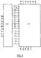
Le système de la Fig. 1 comprend une file d'attente d'entrée FiFo, une mémoire d'état MCO, associée à une unité arithmétique et logique UAL et à un multiplexeur d'adressage MX1, une mémoire d'adresses disponibles MAD associée à un multiplexeur d'adressage MX2, une mémoire tampon MT associée à un multiplexeur d'adressage MX3, des portes ET P1 et P2, une base de temps BT et une unité de commande à microprocesseur UC.The system of FIG. 1 includes a queue FiFo input, an MCO state memory, associated with a unit arithmetic and logic UAL and to an addressing multiplexer MX1, an available address memory MAD associated with a addressing multiplexer MX2, a buffer memory MT associated with an address multiplexer MX3, AND gates P1 and P2, a BT time base and a microprocessor control unit UC.
A l'entrée de la mémoire d'attente FiFo est appliqué le multiplex entrant XE. Les portes P1 délivrent le multiplex sortant XS.The FiFo standby memory input is applied incoming multiplex XE. The P1 gates deliver the multiplex outgoing XS.
Dans l'exemple de réalisation décrit, le multiplex XE est
un multiplex temporel asynchrone du type de celui qui est décrit
dans le document EP-A-108 028, mais dont les paquets, maintenant
appelés "cellules", sont supposés avoir été mis sous forme
parallèle à 424 bits. Cette taille de 424 bits correspond à celle
d'une cellule qui a été adoptée en juin 1989 par le CCITT. La
mémoire FiFo est une file d'alignement, semblable à celle qui est
décrite dans le document EP-A-113 307, dont le rôle est d'adapter
le débit entrant sur l'horloge locale t du système de la Fig. 1.
Chaque cellule sortant de la file FiFo est donc synchrone de
l'horloge locale et est présentée sur un faisceau Fe de 424 fils,
dont les seize premiers EQe transmettent les seize premiers bits
qui constituent l'étiquette Vcie qui identifie le circuit virtuel
qui achemine la cellule, c'est-à-dire qui identifie la communication
concernée. La file FiFo a encore une sortie PP qui porte un
signal du même nom qui indique si l'intervalle de temps entrant
est libre ou occupé. Le signal PP est obtenu comme montré à la
Fig. 1 du document EP-A-113 307. Il en résulte un faisceau de
425 fils sortant de la mémoire FiFo, le 425e fil portant le signal
PP et étant relié à l'entrée du même nom du circuit UAL.In the embodiment described, the XE multiplex is an asynchronous time multiplex of the type described in document EP-A-108 028, but whose packets, now called "cells", are assumed to have been placed under form parallel to 424 bits. This size of 424 bits corresponds to that of a cell which was adopted in June 1989 by the CCITT. The FiFo memory is an alignment file, similar to that which is described in the document EP-A-113 307, the role of which is to adapt the flow entering on the local clock t of the system of FIG. 1. Each cell leaving the FiFo queue is therefore synchronous with the local clock and is presented on a Fe beam of 424 wires, of which the first sixteen EQe transmit the first sixteen bits which constitute the label Vcie which identifies the virtual circuit which routes the cell, that is to say which identifies the communication concerned. The FiFo queue also has a PP output which carries a signal of the same name which indicates whether the incoming time interval is free or busy. The signal PP is obtained as shown in FIG. 1 of EP-A-113 307. The
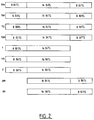
La mémoire d'états MCO est une mémoire vive à accès aléatoire comportant autant de zones que de communications que peut traiter le système. Chaque zone est divisée en six sections respectivement destinées à mémoriser:
- l'heure d'émission théorique de la dernière cellule arrivée tde,
- la période minimale théorique pm,
- l'heure d'émission théorique de la dernière cellule émise tdl,
- le délai maximum dm,
- le nombre NM, et
- le nombre N.
- the theoretical emission time of the last arriving cell tde ,
- the theoretical minimum period pm ,
- the theoretical emission time of the last cell emitted tdl ,
- the maximum delay dm ,
- the NM number, and
- the number N.
La mémoire MCO a six entrées a1 à a6, correspondant respectivement aux six sections mentionnées ci-dessus. Elle comporte également six sorties portant respectivement les mêmes désignations que les sections. Enfin, son entrée d'adressage est reliée à la sortie du multiplexeur à trois entrées MX1.The MCO memory has six entries a1 to a6, corresponding respectively to the six sections mentioned above. It involves also six outputs carrying the same respectively designations as sections. Finally, its addressing input is connected to the output of the multiplexer with three inputs MX1.
La première entrée du multiplexeur MX1 est reliée au faisceau EQe portant l'étiquette Vcie de la cellule entrante, sa seconde entrée est reliée au faisceau EQs portant l'étiquette vcis de la cellule sortante, et sa troisième entrée UCa est reliée à une sortie correspondante de l'unité de commande UC. L'entrée de commande du multiplexeur MX1 est reliée aux sorties E, S et U de la base de temps BT.The first input of the MX1 multiplexer is connected to the EQe beam bearing the label Vcie of the incoming cell, its second input is connected to the EQs beam carrying the vcis label of the outgoing cell, and its third input UCa is connected to a corresponding output of the control unit UC. Entrance MX1 multiplexer control module is connected to outputs E, S and U of the BT time base.
La base de temps BT délivre l'heure locale t dont chaque temps élémentaire correspond à la réception d'une cellule entrante et à l'émission d'une cellule sortante. Comme le montre la Fig. 2, l'heure t, servant à suivre la chronologie des événements, est donnée sur vingt-quatre bits dont une première partie de poids forts composée de huit bits et suivie d'une seconde partie de poids plus faible de seize bits. Comme on le verra plus tard, la première partie permet de repérer les événements à long terme et la seconde sert a l'adressage de la mémoire MT et donc à repérer les événements dans chaque cycle de fonctionnement de la mémoire MT.The time base BT delivers the local time t , each elementary time of which corresponds to the reception of an incoming cell and to the emission of an outgoing cell. As shown in Fig. 2, the hour t , used to follow the chronology of events, is given on twenty-four bits including a first most significant part composed of eight bits and followed by a second least significant part of sixteen bits. As will be seen later, the first part makes it possible to locate long-term events and the second is used for addressing the MT memory and therefore for locating the events in each operating cycle of the MT memory.
L'heure tde définie plus haut est donnée sur trente-deux bits dont une première partie de huit bits et une seconde de seize bits, comme pour t, plus une troisième partie de huit bits de poids faibles constituant une partie décimale dont on verra le rôle plus tard. En fonctionnement normal, l'heure tse se déduit de l'heure théorique d'émission de la cellule précédente de la même communication en y ajoutant la valeur pm qui représente la période minimale théorique de réémission des cellules de la communication concernée. L'heure tde est dite théorique car l'heure réelle d'émission de la cellule concernée pourra en différer, étant donné les conflits possibles entre les temps d'émission théoriques de cellules appartenant à des communications différentes.The time tde defined above is given on thirty-two bits including a first part of eight bits and a second of sixteen bits, as for t , plus a third part of eight least significant bits constituting a decimal part of which we will see the role later. In normal operation, the time tse is deduced from the theoretical time of emission of the previous cell of the same communication by adding to it the value pm which represents the theoretical minimum period of re-transmission of the cells of the communication concerned. The time tde is said to be theoretical because the actual time of emission of the cell concerned may differ from it, given the possible conflicts between the theoretical times of emission of cells belonging to different communications.
La période pm est donnée sur vingt-quatre bits dont la partie de seize bits servant indirectement a l'adressage de la mémoire MT et la partie décimale de huit bits. La période pm correspond au temps minimum qui doit théoriquement séparer les temps de réémission de deux cellules consécutives pour éviter l'effet de "grumeaux" et, par conséquent, lisser le débit des cellules. La partie décimale permet de sélectionner un débit quelconque qui n'est pas nécessairement un sous-multiple du débit du multiplex sortant XS.The period pm is given over twenty-four bits, the part of which is sixteen bits used indirectly for addressing the memory MT and the decimal part of eight bits. The period pm corresponds to the minimum time which must theoretically separate the re-emission times of two consecutive cells to avoid the effect of "lumps" and, consequently, to smooth the flow of the cells. The decimal part makes it possible to select any bit rate which is not necessarily a submultiple of the bit rate of the outgoing multiplex XS.
L'heure d'émission théorique de la dernière cellule émise tdl est codée sur trente-deux bits, comme tde, correspond à l'heure théorique à laquelle la dernière cellule de la communication concernée aurait dû être émise, même si son heure réelle d'émission a été un peu plus tardive.The theoretical transmission time of the last cell transmitted tdl is coded in thirty-two bits, as tde , corresponds to the theoretical time at which the last cell of the communication concerned should have been transmitted, even if its actual time d was a little later.
Le délai maximum dm est codé sur vingt-quatre bits, comme pm, et correspond au temps de retard maximum admissible que peut prendre une cellule dans le réseau, compte tenu de la dispersion de temps de propagation admise qui a été mentionnée dans le préambule. Pour tenir compte de cette dispersion, on accepte de lisser les débits jusqu'à cette valeur de temps dm. Si, par suite de rafales de cellules consécutives dans la même communication on ne peut garantir ce délai, la cellule concernée est détruite. Le délai dm peut varier en fonction d'éventuelles priorités entre des cellules de communications différentes.The maximum delay dm is coded on twenty-four bits, like pm , and corresponds to the maximum admissible delay time that a cell can take in the network, taking into account the accepted propagation time dispersion which was mentioned in the preamble. To take account of this dispersion, we agree to smooth the flow rates up to this time value dm . If, as a result of consecutive bursts of cells in the same communication, this delay cannot be guaranteed, the cell concerned is destroyed. The delay dm can vary according to possible priorities between different communication cells.
La base de temps BT délivre, en plus de l'heure locale t et pour chaque temps élémentaire, six signaux successifs t1 à t6 qui occupent ensemble un temps élémentaire. Les temps t1 et t2 sont utilisés pour le traitement correspondant à l'arrivée d'une cellule entrante, les temps t3 et t4 pour le traitement correspondant à l'émission d'une cellule sortante, et les temps t5 et t6 pour le traitement de l'accès à la mémoire MCO par l'unité de commande UC. De plus, les sorties t1 et t2 sont réunies pour délivrer le signal E, les sorties t3 et t4 pour donner le signal S et les sorties t5 et t6 pour donner le signal U. Les signaux E, S et U servent notamment à commander les multiplexeurs MX1 à MX3.The time base BT delivers, in addition to the local time t and for each elementary time, six successive signals t1 to t6 which together occupy an elementary time. Times t1 and t2 are used for the processing corresponding to the arrival of an incoming cell, times t3 and t4 for the processing corresponding to the emission of an outgoing cell, and times t5 and t6 for the processing of access to the MCO memory by the control unit UC. In addition, the outputs t1 and t2 are combined to deliver the signal E, the outputs t3 and t4 to give the signal S and the outputs t5 and t6 to give the signal U. The signals E, S and U are used in particular to control the multiplexers MX1 to MX3.
La lecture des mémoires s'effectue en t1, t3 et t5 tandis que la réécriture, après calculs, s'effectue en t2, t4 et t6.The memories are read in t1, t3 and t5 while that the rewriting, after calculations, takes place in t2, t4 and t6.
La mémoire tampon MT est une mémoire vive à accès aléatoire comportant des cases dont le nombre sera défini dans la suite. Chaque case est divisée en quatre sections respectivement destinées à mémoriser:
- le champ des données DON utiles d'une cellule,
- l'étiquette Vcie de la cellule correspondante,
- l'heure théorique tde d'émission de cette cellule, et
- un bit bs qui, quand il est à "1", indique que la case adressée en lecture contient une cellule utile à transmettre.
- the field of useful DON data of a cell,
- the Vcie label of the corresponding cell,
- the theoretical time tde of emission of this cell, and
- a bit bs which, when it is "1", indicates that the box addressed in read contains a useful cell to transmit.
La mémoire MT a quatre entrées correspondant respectivement aux données DON, à l'étiquette Vcie, à l'heure théorique d'émission hte et au bit be. Elle comprend également quatre sorties portant respectivement les références DON, vcis, tdse et bes. Les sorties DON et Vcis sont regroupées dans un faisceau de 424 fils reliés respectivement aux premières entrées de 424 portes ET P1 dont les secondes entrées sont reliées à la sortie bes. L'entrée d'adressage de la mémoire MT est reliée à la sortie du multiplexeur MX3.The memory MT has four inputs corresponding respectively to the data DON, to the label Vcie, to the theoretical time of transmission hte and to the bit be . It also includes four outputs with the references DON, vcis, tdse and bes respectively. The outputs DON and Vcis are grouped in a bundle of 424 wires connected respectively to the first inputs of 424 AND AND P1 gates whose second inputs are connected to the bes output. The addressing input of the memory MT is connected to the output of the multiplexer MX3.
La première entrée du multiplexeur MX3 est reliée à la sortie de la mémoire MAD et sa seconde entrée reçoit l'heure courante t de la base de temps BT. Son entrée de commande est reliée aux sortie E et S de la base de temps BT.The first input of the multiplexer MX3 is connected to the output of the MAD memory and its second input receives the current time t from the time base BT. Its control input is connected to the E and S outputs of the BT time base.
La mémoire MAD est une mémoire vive à accès aléatoire comportant autant de cases que la mémoire MT, chaque case ayant une capacité de un bit et correspondant biunivoquement à une case de la mémoire MT. Elle a une entrée dispo qui est mise à "1" ou à "0" selon que la mémoire MT est en mode d'écriture ou de lecture. Elle a une sortie Add. Elle comprend deux entrées d'adressage Adr1 et Adr2. L'entrée Adr1 est reliée à la sortie du multiplexeur MX2 dont une entrée est reliée à la sortie Add de la mémoire MAD et dont la seconde entrée reçoit l'heure locale t de la base de temps BT. L'entrée de commande du multiplexeur MX2 a son entrée de commande reliée aux sorties E et S de la base de temps BT. L'entrée d'adressage Adr2 est reliée à la sortie de la porte P2.The MAD memory is a random access random access memory comprising as many cells as the MT memory, each cell having a capacity of one bit and corresponding biunivocally to one cell of the MT memory. It has an available input which is set to "1" or to "0" depending on whether the memory MT is in write or read mode. It has an Add output. It includes two addressing entries Adr1 and Adr2. The input Adr1 is connected to the output of the multiplexer MX2, one input of which is connected to the output Add of the memory MAD and the second input of which receives the local time t from the time base BT. The control input of the multiplexer MX2 has its control input connected to the outputs E and S of the time base BT. The addressing input Adr2 is connected to the output of gate P2.
La sortie Add de la mémoire MAD est reliée à la première entrée du multiplexeur MX3.The MAD memory add output is connected to the first input of the MX3 multiplexer.
Dans la mémoire MAD, une case contient un "0" pour indiquer qu'elle est libre et un "1" pour indiquer qu'elle est occupée. La mémoire MAD fournit en permanence à sa sortie Add l'adresse d'une case libre, cette adresse étant sélectionnée prioritairement à partir de la valeur binaire d'un champ de seize bits extraits de l'heure d'émission théorique hte de la cellule considérée, c'est-à-dire du signal a1, que l'on décrira plus tard, et qui est appliqué à la première entrée des portes P2. Les secondes entrées de ces portes P2 sont reliées à la sortie E de la base de temps BT, ce qui signifie que l'entrée Adr2 de la mémoire MAD n'est active que pendant le traitement d'une cellule entrante et, précisément, pour trouver une adresse Add de case libre dans la mémoire MT. Une mémoire telle la mémoire MAD est décrite dans le document FR-A-2 617 602 intitulé "Circuit pour mémoriser des états de disponibilité de ressources logiques, telles que cellules de mémoire, et établir des adresses de ressources libres". En pratique, la mémoire MAD comprend des moyens pour explorer la case qui est désignée par hte et, quand cette case n'est pas libre, les cases suivantes, et arrêter l'exploration à la première cellule libre, dont l'adresse est alors délivrée par Add.In the MAD memory, a box contains a "0" to indicate that it is free and a "1" to indicate that it is occupied. The MAD memory provides permanently at its Add output the address of a free cell, this address being selected in priority from the binary value of a field of sixteen bits extracted from the theoretical transmission time hte of the cell considered, that is to say of the signal a1 , which will be described later, and which is applied to the first input of the doors P2. The second inputs of these doors P2 are connected to the output E of the time base BT, which means that the input Adr2 of the memory MAD is only active during the processing of an incoming cell and, precisely, for find a free add address in the MT memory. A memory such as the MAD memory is described in document FR-A-2 617 602 entitled "Circuit for memorizing the availability states of logical resources, such as memory cells, and establishing addresses of free resources". In practice, the memory MAD includes means for exploring the box which is designated by host and, when this box is not free, the following boxes, and stopping the exploration at the first free cell, whose address is then issued by Add.
L'unité arithmétique et logique UAL associée à la mémoire MCO est représentée dans le bloc-diagramme de la Fig. 3. Il comprend une partie arithmétique UAR et une partie de décisions logiques UDL. La partie UAR, Fig. 4, comprend quatre additionneurs ADD1 à ADD4, un circuit de test de voisinage à zéro TVZ, cinq portes OU-exclusif P3 à P7 et cinq comparateurs COM1 à COM5.The arithmetic and logic unit UAL associated with memory MCO is represented in the block diagram of FIG. 3. He includes a UAR arithmetic part and a decision part UDL logic. The PSU part, Fig. 4, includes four adders ADD1 to ADD4, a TVZ zero neighborhood test circuit, five OR-exclusive doors P3 to P7 and five comparators COM1 to COM5.
Le circuit UAR comporte les entrées tde, tdl, dm, E, L, N, NM, t et pm. Il comporte également les sorties t-pm, N-+1, tse, b1, b2, b3, c1, c2, d1, e1, e2, f1 et f2.The UAR circuit has the inputs tde , tdl , dm , E , L , N , NM, t and pm . It also includes the outputs t-pm , N- + 1 , tse , b1 , b2 , b3 , c1 , c2 , d1 , e1 , e2 , f1 and f2 .
Le circuit ADD1 est un additionneur arithmétique qui a ses deux entrées reliées respectivement aux entrées tde et pm, et sa sortie à la sortie tse qui délivre l'heure (tde+pm).The circuit ADD1 is an arithmetic adder which has its two inputs connected respectively to the inputs tde and pm , and its output to the output tse which delivers the time (tde + pm).
Le circuit ADD2 est un additionneur arthmétique qui a trois
entrées dont l'une est reliée à l'entrée tdl, la seconde à
l'entrée dm et la troisième reçoit en permanence la valeur CMT
qui correspond au nombre de cases dans la mémoire MT. A titre
d'exemple, cette valeur peut être de 216, soit 65 536. L'exposant
16 correspond aux seize bits de la seconde partie de t, Fig. 2.
Les huit bits de poids fort de t permettent de ne pas avoir de
valeur zéro à chaque cycle de la mémoire tampon MT, mais un
passage par zéro uniquement tous les 224 temps élémentaires de
la base de temps BT, ce qui correspond à une période T de
celle-ci.The ADD2 circuit is an arthmetic adder which has three inputs, one of which is connected to the tdl input, the second to the dm input and the third permanently receives the value CMT which corresponds to the number of boxes in the memory MT. For example, this value can be 2 16 , or 65,536. The
La sortie P de l'additionneur ADD2, qui délivre la valeur
(
Le circuit ADD3 est un additionneur algébrique qui a deux entrées de commande respectivement reliées aux entrées E et L, et deux entrées dont l'une est reliée à l'entrée N et l'autre reçoit en permanence la valeur "1". Ainsi, quand l'entrée E est activée, le circuit ADD3 ajoute "1" à la valeur N tandis que quand l'entrée L est activée, il soustrait "1" de la valeur N. Ainsi, la sortie du circuit ADD3 délivre soit (N+1), soit (N-1), et est reliée à la sortie N-+1 et à la première entrée du comparateur COM3.The ADD3 circuit is an algebraic adder which has two control inputs respectively connected to inputs E and L , and two inputs, one of which is connected to input N and the other permanently receives the value "1". Thus, when the input E is activated, the circuit ADD3 adds "1" to the value N while when the input L is activated, it subtracts "1" from the value N. Thus, the output of the circuit ADD3 delivers either (N + 1), that is (N-1), and is connected to the output N- + 1 and to the first input of the comparator COM3.
Le circuit ADD4 est un soustracteur arithmétique qui a ses deux entrées reliées respectivement aux entrées t et pm. Sa sortie délivre la valeur (t-pm) et est reliée à la sortie t-pm.The ADD4 circuit is an arithmetic subtractor which has its two inputs connected respectively to the inputs t and pm . Its output delivers the value (t-pm) and is linked to the t-pm output.
Le circuit TVZ a trois entrées z1 à z3 et une sortie Y. Les entrées z1 à z3 sont respectivement reliées aux fils de bit de poids fort de l'entrée tdl, de la sortie P de l'additionneur ADD2 et de l'entrée t, ces fils étant également respectivement reliés aux premières entrées des portes P4 à P6. La sortie Y est à "1" quand, parmi les trois bits de poids forts appliqués à ses entrées, la valeur binaire de l'un d'entre eux diffère de celles des deux autres. La sortie Y est reliée aux secondes entrées des portes P4 à P6. Par ailleurs, le fil de bit de poids fort de l'entrée tde est relié à la première entrée de la porte P3 dont la seconde entrée est reliée à la sortie Y du circuit TVZ. Enfin, le fil de bit de poids fort de la sortie tse est relié à la première entrée de la porte P7 dont la seconde entrée est aussi reliée à la sortie Y.The TVZ circuit has three inputs z1 to z3 and one output Y. The inputs z1 to z3 are respectively connected to the most significant bit wires of the input tdl , of the output P of the adder ADD2 and of the input t , these wires also being respectively connected to the first inputs of the doors P4 to P6. The output Y is at "1" when, among the three most significant bits applied to its inputs, the binary value of one of them differs from those of the other two. The output Y is connected to the second inputs of the doors P4 to P6. Furthermore, the most significant bit wire of the input tde is connected to the first input of the gate P3, the second input of which is connected to the output Y of the TVZ circuit. Finally, the most significant bit wire of the output tse is connected to the first input of the gate P7, the second input of which is also connected to the output Y.
Dans le cas où Y = 0, le bit de poids fort de chacune des valeurs tde, tse, tdl, P et t n'est pas altéré en passant dans sa porte OU-exclusif associée. Dans le cas où Y = 1, le bit de poids fort change de valeur à la sortie des portes P3 à P7, ce qui conduit, une fois qu'il a été associé au reste des bits de poids faible, à avoir toutes les valeurs dans une zone ne comprenant pas la valeur zéro d'un cycle complet de la base de temps BT et donc de pouvoir les comparer, sans ambiguïté, dans les comparateurs COM1, COM2, COM4 et COM5, autour de la valeur T/2.In the case where Y = 0, the most significant bit of each of the values tde , tse , tdl , P and t is not altered by passing through its associated OR-exclusive gate. In the case where Y = 1, the most significant bit changes value at the output of the doors P3 to P7, which leads, once it has been associated with the rest of the least significant bits, to have all the values in a zone not including the zero value of a complete cycle of the LV time base and therefore of being able to compare them, without ambiguity, in the comparators COM1, COM2, COM4 and COM5, around the value T / 2.
Le comparateur COM1 a ses deux entrées td1c et tdec respectivement reliées aux sorties des portes P4 et P3. Sa sortie b1 est activée quand tdec est supérieur tdlc, la sortie b2 est activée quand tdle est égal à tdlc, et la sortie b3 est activée quand tdec est inférieur à tdlc.The comparator COM1 has its two inputs td1c and tdec respectively connected to the outputs of the doors P4 and P3. Its output b1 is activated when tdec is greater than tdlc , the output b2 is activated when tdle is equal to tdlc , and the output b3 is activated when tdec is less than tdlc .
Le comparateur COM2 a une entrée tc reliée à la sortie de la porte P6 et une entrée td1c reliée à la sortie de la porte P4. Sa sortie c1 est activée quand tc est inférieur à tdlc et sa sortie c2 quand tc est égal ou supérieur à tdlc. The comparator COM2 has an input tc connected to the output of the gate P6 and an input td1c connected to the output of the gate P4. Its output c1 is activated when tc is less than tdlc and its output c2 when tc is equal to or greater than tdlc .
Le comparateur COM3 a sa première entrée qui reçoit N-+1 et sa seconde entrée reliée à l'entrée NM. Sa sortie d1 est activée quand N-+1 est supérieur NM.The comparator COM3 has its first input which receives N- + 1 and its second input connected to the input NM . Its output d1 is activated when N- + 1 is greater than NM .
Le comparateur COM4 a une entrée tc reliée à la sortie de la porte P6 pour le bit de poids fort et à l'entrée t pour les bits de poids faible et une entrée Pc reliée à la sortie de la porte P5 pour le bit de poids fort et la sortie P pour les reste des bits de poids faible. Sa sortie e1 est activée quand tc est supérieur Pc et sa sortie e2 est activée quand tc est égal ou inférieur à Pc.Comparator COM4 has an input tc connected to the output of gate P6 for the most significant bit and to input t for the least significant bits and an input Pc connected to the output of gate P5 for the weight bit strong and the P output for the rest of the least significant bits. Its output e1 is activated when tc is greater than Pc and its output e2 is activated when tc is equal to or less than Pc .
Le comparateur COM5 a une entrée tc reliée en parallèle sur l'entrée tc du comparateur COM4 et une entrée tsec reliée à la sortie de la porte P7 pour le fil de poids fort et à la sortie de l'additionneur ADD1 pour le reste des bits de poids faible. Sa sortie f1 est activée quand tc est inférieur à tsec ce qui est un cas normal d'un premier type tandis que sa sortie f2 est activée quand tc est supérieur à tsec ce qui est un cas normal d'un second type.The comparator COM5 has an input tc connected in parallel to the input tc of the comparator COM4 and an input tsec connected to the output of the gate P7 for the most significant wire and to the output of the adder ADD1 for the rest of the bits of low weight. Its output f1 is activated when tc is less than tsec which is a normal case of a first type while its output f2 is activated when tc is greater than tsec which is a normal case of a second type.
Le signal de sortie tse produit par l'additionneur ADD1 correspond à une heure qui est la somme de l'heure théorique d'émission de la cellule précédente tde et de la période minimum pm. La Fig. 2 montre que l'heure tse (tde+pm) est, comme tde, codée sur trente-deux bits dont une partie décimale. Le signal t-pm produit par le soustracteur ADD4 correspond à une heure qui précède le temps courant t d'une valeur égale à la période minimale pm. L'heure t-pm est aussi codée sur trente-deux bits dont une partie décimale. Elle est utilisée dans le cas de réinitialisation, comme on le verra dans la suite en relation avec la Fig. 7. Les signaux NM et N-+1 sont codés sur vingt-quatre bits, sans partie décimale. Le signal NM correspond à un nombre qui représente, pour une communication, le nombre maximum de cellules en attente dans la mémoire MT. Le signal N-+1 est également un nombre qui est comparé au nombre NM dans le comparateur COM3. Le signal P, produit par l'additionneur ADD2, correspond à une heure qui est la somme de l'heure tdl, c'est-à-dire l'heure d'émission théorique de la dernière cellule émise, plus le délai maximum dm entre deux cellules, plus le nombre de cases de la mémoire MT. Il est donc certain qu'à l'heure P, toutes les cellules en attente dans la mémoire MT ont été émises, d'où l'intérêt de la comparaison du temps courant t avec le temps P, comme on le verra plus loin.The output signal tse produced by the adder ADD1 corresponds to an hour which is the sum of the theoretical hour of emission of the previous cell tde and the minimum period pm . Fig. 2 shows that the time tse ( tde + pm ) is, like tde , coded on thirty-two bits including a decimal part. The signal t-pm produced by the subtractor ADD4 corresponds to an hour preceding the current time t by a value equal to the minimum period pm . The time t-pm is also coded on thirty-two bits, part of which is a decimal. It is used in the case of reinitialization, as will be seen below in relation to FIG. 7. The signals NM and N- + 1 are coded on twenty-four bits, with no decimal part. The signal NM corresponds to a number which represents, for a communication, the maximum number of cells waiting in the memory MT. The signal N- + 1 is also a number which is compared to the number NM in the comparator COM3. The signal P , produced by the adder ADD2, corresponds to an hour which is the sum of the hour tdl , that is to say the theoretical emission time of the last cell emitted, plus the maximum delay dm between two cells, plus the number of boxes in the MT memory. It is therefore certain that at time P , all of the cells waiting in memory MT have been sent, hence the interest in comparing the current time t with time P , as will be seen below.
Le signal b1 du comparateur COM1 est à "1" quand tdec est supérieur à tdlc, ce qui exprime que, à l'arrivée de la cellule faisant partie d'une correspondance, l'heure théorique d'émission de la cellule qui est arrivée juste avant est plus tardive que l'heure théorique à laquelle la dernière cellule de la même communication a été émise. Il s'agit d'un cas normal. Le signal b2 à "1" correspond aussi à un cas normal, celui où les deux heures théoriques sont égales. Par contre, le signal b3 à "1" exprime un cas de faute. Il n'est pas possible que l'heure théorique d'émission d'une cellule appartenant à une conversation précède l'heure théorique d'une cellule de la même conversation déjà émise.The signal b1 of the comparator COM1 is at "1" when tdec is greater than tdlc , which expresses that, on arrival of the cell forming part of a correspondence, the theoretical time of emission of the cell which has arrived just before is later than the theoretical time at which the last cell of the same communication was sent. This is a normal case. The signal b2 at "1" also corresponds to a normal case, that where the two theoretical hours are equal. On the other hand, the signal b3 at "1" expresses a case of fault. It is not possible that the theoretical time of emission of a cell belonging to a conversation precedes the theoretical time of a cell of the same conversation already transmitted.
Le signal c1 produit par le comparateur COM2 à "1" exprime que tc est inférieur à tdlc. Il s'agit d'un cas de faute, étant donné que tdlc correspond, au temps tc, à une cellule déjà émise. Le signal de sortie c2 à "1" correspond à un cas normal.The signal c1 produced by the comparator COM2 at "1" expresses that tc is less than tdlc . It is a case of fault, given that tdlc corresponds, at time tc , to a cell already transmitted. The output signal c2 at "1" corresponds to a normal case.
Le signal de sortie d1 du comparateur COM3 à "1" correspond au cas où la mémoire accepterait un nombre de cellules d'un conversation supérieure à ce qui a été convenu au début de la conversation, le nombre convenu étant NM. C'est donc aussi un cas de faute.The output signal d1 of comparator COM3 to "1" corresponds in case the memory accepts a number of cells of a conversation greater than what was agreed at the beginning of the conversation, the agreed number being NM. So it's also a case of fault.
Le signal de sortie el du comparateur COM4 à "1" exprime que tc est supérieur à Pc. Le signal e2 à "1" correspond à un cas normal.The output signal el of the comparator COM4 at "1" expresses that tc is greater than Pc . The signal e2 at "1" corresponds to a normal case.
Le signal de sortie f1 du comparateur COM5 à "1" exprime que tc est inférieur ou égal à tsec ce qui correspond à un cas normal d'un premier type, comme on le verra dans la suite. Le signal de sortie f2 à "1" exprime que tc est supérieur à tsec, ce qui correspond à un cas normal d'un second type.The output signal f1 of the comparator COM5 to "1" expresses that tc is less than or equal to tsec which corresponds to a normal case of a first type, as will be seen below. The output signal f2 at "1" expresses that tc is greater than tsec , which corresponds to a normal case of a second type.
Les signaux f1 et f2 du comparateur COM5 correspondent à deux types de cas normaux comme on le verra plus tard.The signals f1 and f2 of the comparator COM5 correspond to two types of normal cases as will be seen later.
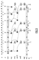
Avant de considérer en détail comment le circuit de décisions logiques UDL traite les différents cas en fonction des signaux b1 à e2 qui lui sont appliqués, on va illustrer en relation avec les Figs. 5 et 6 deux cas de fonctionnements courants et normaux, la valeur de pm étant de quatre temps élémentaires.Before considering in detail how the logic decision circuit UDL treats the different cases as a function of the signals b1 to e2 which are applied to it, we will illustrate in relation to FIGS. 5 and 6 two cases of current and normal operations, the value of pm being four elementary times.
Dans les diagrammes temporels de la Fig. 5:
- la ligne t) montre partiellement le déroulement de l'heure locale t, soit ici les temps élémentaires t19 à t41,
- la ligne i) indique les cellules entrantes de la conversation i, soit ici i1 à i6, étant supposé qu'il ne s'agit pas d'un début de conversation,
- la ligne tde) montre les différentes valeurs tde inscrites successivement dans la zone correspondant à la conversation i de la mémoire MCO,
- la ligne tse) indique les différentes valeurs de tse à la sortie correspondante du circuit UAR,
- la ligne hte) indique les valeurs successives de hte,
- la ligne Adr2) indique les différents adresses initiales appliquées à la mémoire MAD pour qu'elle cherche l'adresse d'une case suivante disponible dans la mémoire MT,
- la ligne add) indique les adresses de la mémoire MT successivement déterminées par la mémoire MAD, en notant que chaque valeur hte est aussi enregistrée à la même adresse de MT, bien que cette valeur puisse être différente de cette adresse,
- la ligne tdle) indique les valeurs successives de tdle à chaque lecture de cellule, la valeur de tdle étant appelée à être mémorisée sous forme de tdl dans la zone correspondant à la conversation i dans la mémoire, après traitement dans le circuit de décisions logiques UDL,
- la ligne tdl) indique précisément les valeurs successives de tdl,
- la ligne N) indique les nombres successifs de cellules de la conversation i qui sont dans la mémoire MT, et
- la ligne i') indique les temps de sortie des cellules de la conversation i, soit ici i'1 à i'5, correspondant à i1 à i5.
- line t) partially shows the progress of local time t , i.e. here the elementary times t19 to t41,
- line i) indicates the incoming cells of conversation i , i.e. here i1 to i6, assuming that this is not the start of a conversation,
- the line tde) shows the different values tde written successively in the zone corresponding to the conversation i of the MCO memory,
- the line tse) indicates the different values of tse at the corresponding output of the UAR circuit,
- the line hte) indicates the successive values of hte ,
- the line Adr2) indicates the various initial addresses applied to the memory MAD so that it searches for the address of a next box available in the memory MT,
- the line add) indicates the addresses of the memory MT successively determined by the memory MAD, by noting that each hte value is also recorded at the same address of MT, although this value can be different from this address,
- the line tdle) indicates the successive values of tdle at each cell reading, the value of tdle being called to be stored in the form of tdl in the zone corresponding to the conversation i in the memory, after processing in the logic decision circuit UDL ,
- the line tdl) indicates precisely the successive values of tdl ,
- line N) indicates the successive numbers of cells of conversation i which are in the memory MT, and
- the line i ') indicates the exit times from the cells of conversation i , here i'1 to i'5, corresponding to i1 to i5.
Dans les diagrammes temporels de la Fig. 6, on a adopté les mêmes conventions.In the time diagrams in Fig. 6, we adopted the same conventions.
Dans le cas de la Fig. 5, les cellules i1 à i5 arrivent à l'entrée du système de l'invention en respectant la période pm de quatre temps élémentaires, sauf pour i4 qui arrive avec un temps de retard. La recherche d'une adresse libre dans la mémoire MAD est immédiate, sauf pour la mémorisation de la cellule i2. Donc, les cellules i'1 à i'5 sortent à peu près espacées comme sont arrivées les cellules i1 à i5. On rappelle que la période pm est la période théorique minimum d'espacement entre deux cellules réémises. Dans le cas de la Fig. 5, on a supposé que les cellules entrantes respectaient pratiquement cette même période pm et on constate que normalement les cellules réémises la respectent aussi.In the case of FIG. 5, cells i1 to i5 arrive at the input of the system of the invention respecting the period pm of four elementary times, except for i4 which arrives with a delay time. The search for a free address in the MAD memory is immediate, except for the storage of cell i2. Therefore, cells i'1 to i'5 come out approximately spaced as cells i1 to i5 arrived. It will be recalled that the period pm is the minimum theoretical period of spacing between two reemitted cells. In the case of FIG. 5, it has been assumed that the incoming cells respect practically this same period pm and it is found that normally the re-emitted cells also respect it.
Dans le cas illustré à la Fig. 6, à partir de la cellule i2, la période minimale pm n'est plus respectée, les cellules entrantes i3 à i5 arrivent très rapprochées, alors que la cellule suivante arrive nettement plus tard. Mais on notera que les cellules sortantes i'1 à i'4 sont bien espacées, ce qui confirme que le système de la demande principale effectue un lissage. La Fig. 6 montre également que le nombre N peut augmenter rapidement en cas de rafales. Si la rafale i3 à i5 avait continué, le nombre N aurait pu dépasser un maximum NM, ce qui aurait entraíné l'élimination des dernières cellules de la rafale.In the case illustrated in FIG. 6, from cell i2, the minimum period pm is no longer respected, the incoming cells i3 to i5 arrive very close together, while the next cell arrives much later. But it will be noted that the outgoing cells i'1 to i'4 are well spaced, which confirms that the main demand system performs a smoothing. Fig. 6 also shows that the number N can increase rapidly in the event of gusts. If the burst i3 to i5 had continued, the number N could have exceeded a maximum NM, which would have resulted in the elimination of the last cells of the burst.
Les deux cas illustrés aux Figs. 5 et 6 ne constituent que des exemples de cas normaux qui permettent d'apprécier le cas de fautes ou d'autres cas normaux qui vont maintenant être décrits en détail en considérant les Figs. 7 à 9.The two cases illustrated in Figs. 5 and 6 are only examples of normal cases which allow to assess the case faults or other normal cases that will now be described in detail by considering Figs. 7 to 9.
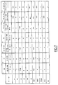
Comme le montre la Fig. 3, les entrées du circuit de décisions logiques sont: N-+1, t-pm, tse, b1, b2, b3, c1, c2, d1, e1, e2, f1, f2, AM, bs, PP, tdle, t, et t1 à t6. On va maintenant décrire successivement les traitements exécutés à l'arrivée d'une cellule entrante, à l'émission d'une cellule sortante et à l'accès de l'unité centrale.As shown in Fig. 3, the circuit inputs logical decisions are: N- + 1, t-pm, tse, b1, b2, b3, c1, c2, d1, e1, e2, f1, f2, AM, bs, PP, tdle, t, and t1 to t6. We go now describe successively the treatments executed at the arrival of an incoming cell, on the emission of a cell outgoing access to the central unit.
A l'arrivée d'une cellule entrante, celle-ci est traitée en
t1, puis t2, Fig. 7. La zone de la mémoire MCO, qui correspond
à la communication i à laquelle appartient la cellule entrante,
est adressée, à travers le multiplexeur MX1 commuté par l'entrée
Les différentes cases indiquées dans le tableau de la
Fig. 7 représentent les actions à entreprendre en fonction des
événements définis par les signaux b1 à f2 (première ligne),
associés aux conditions inscrites à la deuxième ligne. On rencontre
donc les cas suivants:
De plus, les seize bits du signal a1, correspondant aux seize bits de poids faible de t, sont appliqués, par les portes P2 ouvertes par le signal E, à l'entrée Adr2 de la mémoire MAD qui va chercher l'adresse égale ou supérieure à t d'une case libre dans la mémoire MT. Le faisceau des 32 fils de a1, toujours par les portes P2, est prolongé vers l'entrée hte de la mémoire MT. Le fil be est à "1". La mémoire MT adressée par le multiplexeur MX3 mémorise la cellule entrante, l'heure hte et le bit be dans la case correspondante.
Enfin, la mémoire MAD inscrit le bit "1" présent à l'entrée dispo reliée au fil be dans la case d'adresse Add, l'adressage d'écriture étant transmis par le multiplexeur MX2 commandé par E.
Ce cas ne peut normalement se produire et c'est donc un cas de faute. On décide de prendre la cellule entrante en compte et on prend les mêmes actions qu'en 1) ci-dessus.
Ce cas signifie qu'au bout du temps P, qui est la somme de tdl, de dm et d'un cycle de lecture de la mémoire MT,
En t1, à la lecture de la zone de la mémoire MCO, il apparaít que le nombre N de cellules de la communication i en attente dans la mémoire MT est supérieur à NM, c'est-à-dire supérieur au nombre convenu lors de l'établissement de la communication i. On prend la décision de ne pas écrire la cellule entrante qui se trouve éliminée, les données déjà existantes dans la zone correspondante de la mémoire MCO étant inchangées.
Ce cas correspond à une absence de cellule à émettre pour la communication i. On prend la cellule entrante en compte et les actions sont les mêmes qu'en 1) ci-dessus.
On notera que ce cas correspond au cas initial après établissement de la communication i.
C'est un cas normal de fonctionnement du second type. La cellule entrante va être prise en compte, En t2, la valeur de tse va devenir la nouvelle heure tde et, par a1 et les portes P2, va adresser l'entrée Adr2 de la mémoire MAD et la fin des actions va être la même que celle du cas 7) ci-dessous. De plus, la valeur de N va être incrémentée d'une unité.
C'est un cas normal de fonctionnement de premier type. La cellule entrante va être prise en compte. En t2, la valeur de tse va devenir la nouvelle heure tde et, par a1 et les portes P2, va adresser l'entrée Adr2 de la mémoire MAD. Les contenus de a2 à a5 sont inchangés. La valeur de N va être incrémentée d'une unité et rangée en a6.
Ce septième cas est illustré par les diagrammes des Figs. 5
In addition, the sixteen bits of the signal a1, corresponding to the sixteen least significant bits of t , are applied, by the doors P2 opened by the signal E, to the input Adr2 of the memory MAD which will seek the equal address or greater than t of a free cell in the MT memory. The bundle of the 32 wires of a1, still through the doors P2, is extended towards the host input of the memory MT. The be wire is at "1". The memory MT addressed by the multiplexer MX3 stores the incoming cell, the host time and the be bit in the corresponding box.
Finally, the MAD memory writes the bit "1" present at the available input connected to the wire be in the Add address box, the write addressing being transmitted by the multiplexer MX2 controlled by E.
This case cannot normally occur and it is therefore a case of fault. We decide to take the incoming cell into account and we take the same actions as in 1) above.
This case means that at the end of time P, which is the sum of tdl , dm and a reading cycle of the memory MT,
In t1, on reading the area of the MCO memory, it appears that the number N of cells of the communication i waiting in the memory MT is greater than NM , that is to say greater than the number agreed upon. establishing communication i . The decision is made not to write the incoming cell which is eliminated, the data already existing in the corresponding area of the MCO memory being unchanged.
This case corresponds to an absence of cell to be sent for communication i . We take the incoming cell into account and the actions are the same as in 1) above.
It will be noted that this case corresponds to the initial case after establishment of the communication i .
This is a normal case of operation of the second type. The incoming cell will be taken into account, In t2, the value of tse will become the new time tde and, by a1 and the doors P2, will address the entry Adr2 of the MAD memory and the end of the actions will be the same as in case 7) below. In addition, the value of N will be increased by one.
It is a normal case of first type operation. The incoming cell will be taken into account. In t2, the value of tse will become the new time tde and, by a1 and the doors P2, will address the entry Adr2 of the memory MAD. The contents of a2 to a5 are unchanged. The value of N will be incremented by one and stored in a6.
This seventh case is illustrated by the diagrams of Figs. 5 and 6.
A l'émission d'une cellule sortante, la zone de la mémoire
MCO, qui correspond à la communication i à laquelle appartient
la cellule sortante, est adressée, à travers le multiplexeur MX1
commuté par l'entrée
Il est important de noter qu'une case de la mémoire MT, donc une cellule, ne peut être lue que si le bit be qui est associé est à "1".It is important to note that a cell in the MT memory, therefore a cell, can only be read if the bit be which is associated is "1".
Les différentes cases indiquées dans le tableau de la
Fig. 8 représentent les actions à entreprendre en fonction des
événements définis par les signaux b1 à f2 (première ligne),
associés aux conditions inscrites à la deuxième ligne. On rencontre
donc les cas suivants:
Ce cas correspond à un cas de faute, comme à l'arrivée d'une cellule entrante, et pour les mêmes raisons. On attribue aux heures tde et tdl la valeur de l'heure courante t et on met N à "0", be à "0", les autres champs pm, dm et NM de la case étant inchangés.
Pour les mêmes raisons que lors de l'arrivée d'une cellule entrante, il s'agit d'un cas de faute et les actions prises sont les mêmes qu'en 1) ci-dessus.
Il s'agit d'un cas anormal. En effet, puisque l'heure tde est égale à l'heure tdl, il n'y a plus de cellule de la communication en attente à émettre. Or l'adressage de la mémoire MCO est effectué par l'étiquette Vcis de la cellule en cours de lecture dans la mémoire MT. De plus, l'heure t supérieure à P indique que, depuis la dernière cellule émise, il s'est écoulé un peu plus d'un cycle de lecture de la mémoire tampon MT. Cela confirme que toutes les cellules auraient dû être lues. On effectue les mêmes actions qu'en 1) ci-dessus.
A noter que si e1 est à "1", mais b2 à "0", cela signifie que la dernière cellule entrante est arrivée très récemment. Il faut alors émettre comme ci-dessous en 4).
Il s'agit d'un cas normal de lecture cellule sortante pour émission. L'heure tdle délivrée par la mémoire MT est utilisée pour remettre à jour, par a3, l'ancienne valeur de l'heure tdl dans la zone correspondante de la mémoire MCO. Par ailleurs, par a6, le nombre N est décrémenté puisque l'additionneur ADD3 du circuit UAR a fonctionné en soustracteur. Par le multiplexeur MX2, commandé par S, la mémoire MAD est adressée par l'heure courante t et le fil be remet la case correspondante de la mémoire MAD à "0", ce qui signifie que cette case redevient libre. Enfin, le fil be remet aussi à "0" le bit correspondant de la mémoire MT. Les autres champs de la zone de la mémoire MCO restent inchangés.
Il s'agit d'un cas normal et on prend les mêmes actions qu'en 4) ci-dessus.
Il s'agit d'un cas de faute puisqu'on lit une cellule et qu'il n'y en a théoriquement plus. On prend donc les mêmes actions qu'en 1) ci-dessus.
This case corresponds to a case of fault, as on the arrival of an incoming cell, and for the same reasons. The hours tde and tdl are assigned the value of the current time t and N is set to "0", be to "0", the other fields pm , dm and NM of the box being unchanged.
For the same reasons as when an incoming cell arrives, it is a case of fault and the actions taken are the same as in 1) above.
It is an abnormal case. In fact, since the time tde is equal to the time tdl , there is no longer a cell in the waiting call to be transmitted. However, the addressing of the memory MCO is carried out by the label Vcis of the cell being read in the memory MT. In addition, the hour t greater than P indicates that, since the last cell transmitted, a little more than one reading cycle of the buffer memory MT has elapsed. This confirms that all of the cells should have been read. The same actions are carried out as in 1) above.
Note that if e1 is at "1", but b2 at "0", it means that the last incoming cell arrived very recently. Then send as below in 4).
This is a normal case of outgoing cell reading for transmission. The time tdle delivered by the memory MT is used to update, by a3, the old value of the time tdl in the corresponding zone of the memory MCO. Furthermore, by a6, the number N is decremented since the adder ADD3 of the UAR circuit has operated as a subtractor. By the multiplexer MX2, controlled by S, the MAD memory is addressed by the current time t and the wire be resets the corresponding box of the MAD memory to "0", which means that this box becomes free again. Finally, the wire be also resets to "0" the corresponding bit of the memory MT. The other fields in the MCO memory area remain unchanged.
This is a normal case and we take the same actions as in 4) above.
This is a case of fault since we read a cell and theoretically there are no more. We therefore take the same actions as in 1) above.
Pour l'accès de l'unité centrale UC à la mémoire MCO, le
multiplexeur MX1 est commuté par le signal
L'accès de l'unité centrale UC à la mémoire MCO correspond à plusieurs fonctions: la mise à jour horaire et l'initialisation d'une communication.The access of the central processing unit UC to the memory MCO corresponds with several functions: time update and initialization of a communication.
Les différentes cases indiquées dans le tableau de la
Fig. 9 représentent les actions à entreprendre pour la mise à
jour horaire en fonction des événements définis par les signaux
b3, c1, b2 et c2 et e2 (première ligne), associés aux conditions
inscrites à la deuxième ligne. On rencontre donc les cas suivants:
Il s'agit d'un cas de faute car l'heure tdl ne peut dépasser l'heure tde. On écrit dans la zone concernée des valeurs de tde et de tdl égale à l'heure courante t, et on donne au nombre N la valeur "0", les autres champs pm, dm et NM étant inchangés.
Il s'agit aussi d'un cas de faute et on prend les mêmes actions qu'en 1) ci-dessus.
Il s'agit du cas normal de remise à l'heure avec aucune cellule en attente d'émission pour la communication considérée. En effet, la communication n'a pas été active pendant un certain temps et les valeurs horaires de tde et de tdl présentes dans la zone de la communication considérée sont dues soit à une activité précédente, soit à une précédente remise à l'heure par l'unité centrale UC. Les actions prises sont les mêmes qu'en 1) ci-dessus.
C'est un cas normal et aucun changement dans les champs de zone n'est entrepris.
C'est un cas normal et aucun changement dans les champs de la zone n'est entrepris.
It is a case of fault because the time tdl cannot exceed the time tde . Values of tde and tdl equal to the current time t are written in the zone concerned, and the number N is given the value "0", the other fields pm , dm and NM being unchanged.
It is also a case of fault and we take the same actions as in 1) above.
This is the normal case of time reset with no cell awaiting transmission for the communication considered. Indeed, the communication was not active for a certain time and the hourly values of tde and tdl present in the area of the communication considered are due either to a previous activity, or to a previous time reset by the central processing unit UC. The actions taken are the same as in 1) above.
This is a normal case and no changes to the zone fields are made.
This is a normal case and no changes to the fields in the area are undertaken.
Dans la seconde fonction, l'unité centrale UC intervient aussi dans la mémoire MCO, soit pour initialiser celle-ci, soit pour établir une nouvelle communication, soit pour une mise à jour. Dans ce cas l'adresse UCa comporte un bit d'adresse sup lémentaire de poids plus fort mis à "1" pour différencier cette fonction de celle d'une simple mise à jour horaire. Il en résulte qu'indépendamment des calculs et des décisions dans l'unité UAL, l'unité centrale UC accède aux fils de sortie a1 à a6 par l'intermédiaire de la liaison AM. Les six sections de la zone considérée sont ainsi positionnées directement. A noter que dans ce cas les heures tde et tdl prennent la valeur de l'heure courante t.In the second function, the central unit UC also intervenes in the memory MCO, either to initialize the latter, or to establish a new communication, or for an update. In this case, the address UCa comprises a bit of additional address of higher weight set to "1" to differentiate this function from that of a simple time update. As a result, independently of the calculations and decisions in the unit UAL, the central unit UC accesses the output wires a1 to a6 via the link AM. The six sections of the area under consideration are thus positioned directly. Note that in this case the times tde and tdl take the value of the current time t .
La mise à jour de la mémoire MCO par l'unité centrale UC a lieu cycliquement. L'unité centrale explore toute la mémoire MCO au moins en un temps inférieur à T/2, où T correspond, comme on l'a déjà mentionné, à un cycle de la base de temps BT. Ansi, l'unité centrale UC maintient toutes les valeurs affectées à une communication à proximité de l'heure exacte t délivrée par la base de temps BT, de façon que toutes ces heures soient toujours distantes les unes des autres d'une valeur inférieure à T/2.The updating of the MCO memory by the central processing unit UC takes place cyclically. The central unit explores all of the MCO memory at least in a time less than T / 2, where T corresponds, as already mentioned, to a cycle of the time base BT. Thus, the central processing unit UC maintains all the values assigned to a communication near the exact time t delivered by the time base BT, so that all these hours are always distant from each other by a value less than T / 2.
De cette façon, si le poids fort d'une quelconque des heures diffère, pour une communication, du poids fort d'une autre heure, c'est que l'ensemble de ces heures se trouvent au voisinage du passage de la base de temps BT à zéro. Il convient, dans ce cas, d'effectuer la comparaison des heures en rajoutant la valeur T/2 à toutes heures avant comparaison; elles se retrouveront au voisinage de T/2 et l'ordre chronologique sera respecté dans les comparaisons. C'est cette addition qui est effectuée ou non, par le circuit TVZ et les portes P3 à P7, Fig. 3.In this way, if the high weight of any of the hours differs, for a communication, from the most significant of a other hour is that all of these hours are at the neighborhood of the passage of the time base BT to zero. he in this case it is advisable to compare the hours in adding the value T / 2 at all hours before comparison; they will be found in the vicinity of T / 2 and the chronological order will be respected in comparisons. It is this addition which is carried out or not, by the TVZ circuit and the doors P3 to P7, Fig. 3.
Le système peut être simplifié en prenant une marge supérieure pour le calcul de la valeur P. On peut n'effectuer des remises à jour que si N=0, lorsque t est supérieur à tde. En effet, si N est différent de zéro, les remises à jour ont lieu en permanence puisque la communication est active.The system can be simplified by taking a higher margin for the calculation of the P value. Updates can only be made if N = 0, when t is greater than tde . Indeed, if N is different from zero, the updates take place permanently since the communication is active.
Si t est inférieur à tde, on tombe dans le cas de faute de non remise à 0 par l'unité centrale ou autres et les remises à jour s'imposent.If t is less than tde , it falls in the case of failure to not reset to 0 by the central unit or others and the updates are required.
Cette simplification conduit à supprimer les champs tdl et
dm dans la mémoire MCO et le champ tdle dans la mémoire MT.
De plus la condition
Si N =0, les pointeurs sont remis à jour dans tous les cas.
De plus, en réception de cellule entrante, celle-ci est prise en
compte et N prend la valeur N = 1. En réémission de cellule
sortante ou mise à jour par l'unité centrale UC, N prend la
valeur 0. Toutes les valeurs sont positionnées comme dans la
colonne 1 des Figs. 7 à 9, sauf que le champ a3 n'existe pas.If N = 0, the pointers are updated in all cases.
In addition, on incoming cell reception, this is taken into account.
account and N takes the value N = 1. In cell retransmission
outgoing or updated by the central processing unit UC, N takes the
Si N est différent de 0 et que t est supérieur à tde, une cellule entrante est prise en compte avec la valeur (N+1) dans le champ a6. Une cellule sortante est prise en compte avec la valeur (N-1) dans le champ a6. La mise à jour par l'unité centrale ne modifie rien.If N is different from 0 and t is greater than tde , an incoming cell is taken into account with the value (N + 1) in field a6. An outgoing cell is taken into account with the value (N-1) in field a6. The update by the central unit does not change anything.
Si t est inférieur à tde, il y a remise à l'heure.If t is less than tde , the time is reset.
A l'initialisation par l'unité centrale UC, les champs tde, pm, tdl et dm sont positionnés à 0, puis les zones correspondant aux circuits virtuels choisis pour véhiculer des communications sont progressivement initialisées, d'abord les chmaps pm et dm, puis les champs tde et tdl par remise à l'heure.On initialization by the central processing unit UC, the fields tde , pm , tdl and dm are positioned at 0, then the zones corresponding to the virtual circuits chosen to convey communications are gradually initialized, first the chmaps pm and dm , then the tde and tdl fields by time reset.
A noter encore que si la mémoire tampon MT déborde, on aura une absence d'adresse libre dans la mémoire MAD et la cellule entrante sera rejetée.Note also that if the buffer MT overflows, we will have an absence of free address in the MAD memory and the cell incoming will be rejected.
Claims (2)
- Method of monitoring the flow of asynchronous time division communications formed from cells carried by an incoming time division multiplex (XE) to deliver an outgoing time division multiplex (XS), each incoming cell being stored in a buffer (MT) at an address (ADD) corresponding to its real time of forwarding (t) on the outgoing time division multiplex (XS), characterised in that it consists in comparing the number of cells (N) of the same communication which are stored in the buffer (MT) and which have not yet been transmitted at the time of arrival of an incoming cell belonging to the said communication with a maximum number (NM) allocated to the communication and, in the case where the first number exceeds the second, not making provision to forward the said incoming cell.
- Means of implementing the method according to claim 1, for monitoring the flow of asynchronous time division communications formed from cells carried by an incoming time division multiplex (XE) to deliver an outgoing asynchronous time division multiplex (XS), each incoming cell being stored in a buffer (MT) at an address (ADD) corresponding to its real time of forwarding (t) on the outgoing time division multiplex (XS), characterised in that said means comprise, besides the buffer (MT), a status memory (MCO) and an arithmetic and logic unit (ALU), the status memory (MCO) being divided into zones, each zone corresponding one-to-one to a communication transmitted by the incoming asynchronous time division multiplex (XE) and comprising two sections, a first section (N) in which is stored the number of cells of the communication which are stored in the buffer (MT) and which have not yet been transmitted at the time of arrival of the incoming cell of the same communication, and a second section (NM) in which is stored the maximum number allocated to the communication, the arithmetic and logic unit (ALU) making the comparison between the first number (N) and the second number (NM) and inhibiting the forwarding of the incoming cell, when the first number exceeds the second.
Applications Claiming Priority (3)
| Application Number | Priority Date | Filing Date | Title |
|---|---|---|---|
| FR909000770A FR2657482B1 (en) | 1990-01-19 | 1990-01-19 | METHOD AND SYSTEM FOR SMOOTHING AND CONTROLLING ASYNCHRONOUS TIME COMMUNICATION RATES. |
| FR9000770 | 1990-01-19 | ||
| EP90460052A EP0438009B1 (en) | 1990-01-19 | 1990-12-19 | Method and system for smoothing and monitoring the data rates of asynchronous time division communications |
Related Parent Applications (2)
| Application Number | Title | Priority Date | Filing Date |
|---|---|---|---|
| EP90460052A Division EP0438009B1 (en) | 1990-01-19 | 1990-12-19 | Method and system for smoothing and monitoring the data rates of asynchronous time division communications |
| EP90460052.5 Division | 1990-12-19 |
Publications (3)
| Publication Number | Publication Date |
|---|---|
| EP0478008A2 EP0478008A2 (en) | 1992-04-01 |
| EP0478008A3 EP0478008A3 (en) | 1992-10-21 |
| EP0478008B1 true EP0478008B1 (en) | 2000-10-25 |
Family
ID=9393038
Family Applications (2)
| Application Number | Title | Priority Date | Filing Date |
|---|---|---|---|
| EP91120628A Expired - Lifetime EP0478008B1 (en) | 1990-01-19 | 1990-12-19 | Method and system for monitoring the data rates of asynchronous time division communications |
| EP90460052A Expired - Lifetime EP0438009B1 (en) | 1990-01-19 | 1990-12-19 | Method and system for smoothing and monitoring the data rates of asynchronous time division communications |
Family Applications After (1)
| Application Number | Title | Priority Date | Filing Date |
|---|---|---|---|
| EP90460052A Expired - Lifetime EP0438009B1 (en) | 1990-01-19 | 1990-12-19 | Method and system for smoothing and monitoring the data rates of asynchronous time division communications |
Country Status (7)
| Country | Link |
|---|---|
| US (2) | US5297140A (en) |
| EP (2) | EP0478008B1 (en) |
| JP (1) | JP2843155B2 (en) |
| AU (2) | AU634622B2 (en) |
| CA (1) | CA2032301C (en) |
| DE (2) | DE69033655T2 (en) |
| FR (1) | FR2657482B1 (en) |
Families Citing this family (20)
| Publication number | Priority date | Publication date | Assignee | Title |
|---|---|---|---|---|
| FR2686205B1 (en) * | 1992-01-14 | 1994-03-25 | Pierre Boyer | METHOD FOR MONITORING CELL FLOW. |
| FR2694671A1 (en) * | 1992-08-06 | 1994-02-11 | Trt Telecom Radio Electr | Device for rearranging virtual circuit rates in asynchronous time division multiplex transmission. |
| EP0602282B1 (en) * | 1992-11-30 | 2002-01-23 | Alcatel | Resequencing means for a cell switching system node |
| FR2699299B1 (en) * | 1992-12-16 | 1995-02-24 | Christian Wipliez | Method for generating cell jitter in an incident signal transmitted in ATM mode and device for implementing it. |
| FR2707023B1 (en) * | 1993-06-24 | 1995-09-22 | Boyer Jacqueline | |
| GB9326276D0 (en) * | 1993-12-23 | 1994-02-23 | Newbridge Network Corp | Frame relay interface |
| DE69422902T2 (en) * | 1994-02-17 | 2000-08-17 | Alcatel Bell Nv | Molding process |
| US5862127A (en) * | 1994-03-18 | 1999-01-19 | Electronics And Telecommunications Research Institute | Method of controlling the peak cell rate spacing of multiplexed ATM traffic |
| JP3277694B2 (en) * | 1994-05-25 | 2002-04-22 | ソニー株式会社 | Communication method |
| US5515363A (en) * | 1994-06-30 | 1996-05-07 | Digital Equipment Corporation | Traffic shaping system with transmit latency feedback for asynchronous transfer mode networks |
| US5724513A (en) * | 1994-06-30 | 1998-03-03 | Digital Equipment Corporation | Traffic shaping system for asynchronous transfer mode networks |
| JP2922119B2 (en) * | 1994-09-01 | 1999-07-19 | 沖電気工業株式会社 | Bandwidth regulation device and packet communication device |
| EP0702473A1 (en) * | 1994-09-19 | 1996-03-20 | International Business Machines Corporation | A method and an apparatus for shaping the output traffic in a fixed length cell switching network node |
| GB9509484D0 (en) * | 1995-05-10 | 1995-07-05 | Gen Datacomm Adv Res | Atm network switch |
| KR100318956B1 (en) * | 1995-12-26 | 2002-04-22 | 윤종용 | Apparatus and method for multiplexing cells in asynchronous transmission mode |
| US5706288A (en) * | 1996-03-27 | 1998-01-06 | Pmc-Sierra, Inc. | Available bit rate scheduler |
| KR100221323B1 (en) * | 1996-12-26 | 1999-09-15 | 전주범 | Method of controlling the cell delay by using the time interval between previous cells at the upc of uni in atm networks |
| FR2763448B1 (en) | 1997-05-13 | 1999-07-16 | Fihem | ATM CELL SPACER |
| FR2763410B1 (en) | 1997-05-13 | 1999-07-23 | Fihem | SORTING DEVICE OF DATA ELEMENTS WITH BINARY SHAFT AND ATM SPACER COMPRISING SUCH A DEVICE |
| US6034960A (en) * | 1997-12-04 | 2000-03-07 | Nortel Networks Corporation | ATM service scheduler using reverse-binary scattering and time-space mapping |
Family Cites Families (13)
| Publication number | Priority date | Publication date | Assignee | Title |
|---|---|---|---|---|
| GB1427319A (en) * | 1972-05-04 | 1976-03-10 | Plessey Co Ltd | Communication systems |
| US4060849A (en) * | 1975-10-28 | 1977-11-29 | Compagnie Internationale Pour L'informatique Cii-Honeywell Bull | Data input and output controller |
| US4475192A (en) * | 1982-02-16 | 1984-10-02 | At&T Bell Laboratories | Data packet flow control scheme for switching networks |
| US4488294A (en) * | 1982-03-30 | 1984-12-11 | At&T Bell Laboratories | Establishing and supporting data traffic in private branch exchanges |
| FR2616024B1 (en) * | 1987-05-26 | 1989-07-21 | Quinquis Jean Paul | SYSTEM AND METHOD FOR PACKET FLOW CONTROL |
| CA1311818C (en) * | 1987-12-29 | 1992-12-22 | Nec Corporation | Time division switching for multi-channel calls using two time switch memories acting as a frame aligner |
| JP2540930B2 (en) * | 1988-02-19 | 1996-10-09 | 日本電気株式会社 | Congestion control device |
| US4899333A (en) * | 1988-03-31 | 1990-02-06 | American Telephone And Telegraph Company At&T Bell Laboratories | Architecture of the control of a high performance packet switching distribution network |
| JPH0785547B2 (en) * | 1988-07-08 | 1995-09-13 | 日本電気株式会社 | Frame converter |
| EP0355243A1 (en) * | 1988-08-26 | 1990-02-28 | International Business Machines Corporation | High capacity timer arrangement |
| JPH02170645A (en) * | 1988-12-22 | 1990-07-02 | Nec Corp | System and equipment for packet transmission |
| US5003535A (en) * | 1989-06-23 | 1991-03-26 | At&T Bell Laboratories | Packet synchronization utilizing a multi-length packet format including check sequences |
| AU625628B2 (en) * | 1989-10-12 | 1992-07-16 | Alcatel N.V. | Device for regulating the throughput of virtual circuits on an asynchronous time-division multiplex transmission channel |
-
1990
- 1990-01-19 FR FR909000770A patent/FR2657482B1/en not_active Expired - Lifetime
- 1990-12-13 US US07/627,044 patent/US5297140A/en not_active Expired - Lifetime
- 1990-12-14 CA CA002032301A patent/CA2032301C/en not_active Expired - Lifetime
- 1990-12-19 EP EP91120628A patent/EP0478008B1/en not_active Expired - Lifetime
- 1990-12-19 DE DE69033655T patent/DE69033655T2/en not_active Expired - Fee Related
- 1990-12-19 EP EP90460052A patent/EP0438009B1/en not_active Expired - Lifetime
- 1990-12-19 DE DE69018052T patent/DE69018052T2/en not_active Expired - Fee Related
-
1991
- 1991-01-16 JP JP345091A patent/JP2843155B2/en not_active Expired - Fee Related
- 1991-01-17 AU AU69417/91A patent/AU634622B2/en not_active Expired
- 1991-12-12 US US07/806,163 patent/US5299191A/en not_active Expired - Fee Related
-
1992
- 1992-01-07 AU AU10082/92A patent/AU632007B2/en not_active Ceased
Also Published As
| Publication number | Publication date |
|---|---|
| EP0478008A3 (en) | 1992-10-21 |
| AU632007B2 (en) | 1992-12-10 |
| DE69018052D1 (en) | 1995-04-27 |
| EP0438009B1 (en) | 1995-03-22 |
| DE69018052T2 (en) | 1995-07-27 |
| CA2032301A1 (en) | 1991-07-20 |
| FR2657482B1 (en) | 1993-12-31 |
| DE69033655D1 (en) | 2000-11-30 |
| JP2843155B2 (en) | 1999-01-06 |
| US5297140A (en) | 1994-03-22 |
| AU1008292A (en) | 1992-02-27 |
| AU634622B2 (en) | 1993-02-25 |
| FR2657482A1 (en) | 1991-07-26 |
| DE69033655T2 (en) | 2001-03-01 |
| AU6941791A (en) | 1991-07-25 |
| EP0478008A2 (en) | 1992-04-01 |
| JPH04212545A (en) | 1992-08-04 |
| CA2032301C (en) | 1996-05-21 |
| EP0438009A1 (en) | 1991-07-24 |
| US5299191A (en) | 1994-03-29 |
Similar Documents
| Publication | Publication Date | Title |
|---|---|---|
| EP0478008B1 (en) | Method and system for monitoring the data rates of asynchronous time division communications | |
| EP0293315B1 (en) | Method and system for controlling the flow of data packets | |
| EP0293314B1 (en) | Method and system for controlling the flow of data packets | |
| EP0451029B1 (en) | Connexion circuit switch for through-connecting frames in an asynchronous digital network | |
| EP0475161B1 (en) | Temporary data storage system having a buffer memory for holding data blocks of fixed or variable length | |
| EP0021917B1 (en) | Terminal concentrator for a data packet transmission and switching network | |
| EP0300941B1 (en) | Switching system for informations with priorities | |
| FR2883117A1 (en) | ARCHITECTURE OF COMMUNICATION NODE IN A GLOBALLY ASYNCHRONOUS CHIP NETWORK SYSTEM. | |
| EP0552121B1 (en) | Method for cell flow control | |
| EP0618749A1 (en) | Apparatus and system for information multiplexing in ATM network | |
| FR2737030A1 (en) | METHOD FOR TRANSFERRING MESSAGES IN A MULTINODAL COMPUTER SYSTEM | |
| EP0602281B1 (en) | Resequencing means for a cell switching system node | |
| EP0920157A1 (en) | Device for managing a shared buffer memory | |
| FR2736779A1 (en) | DATA SWITCHING APPARATUS, FOR EXAMPLE IN ASYNCHRONOUS TRANSPORTATION NETWORKS | |
| EP1557767A1 (en) | Method and system for transmitting messages in an interconnection network | |
| EP0340841B1 (en) | Cross-point element between two data highways | |
| EP0300942B1 (en) | Switching system for data packets with priorities | |
| FR2549673A1 (en) | Elementary switch for automatic switching unit using an asynchronous multiplexing technique. | |
| FR2668324A1 (en) | Method and system for smoothing and monitoring flow rates for asynchronous time-based communications | |
| EP1052573B1 (en) | Method and device for controlling the output-order of temporarily stored data or objects | |
| EP0470875B1 (en) | Communication controller between a computer and a plurality of ISDN terminals | |
| EP1087568B1 (en) | Method and apparatus for transmission circuit management in a network | |
| EP0652662A1 (en) | Waiting queues arrangement to be used at the input stage of a non-blocking space-switching matrix | |
| KR100333475B1 (en) | Rate proportional self-clocked fair queueing apparatus and method for high-speed packet-switched networks | |
| EP0251965B1 (en) | Data packet switching system |
Legal Events
| Date | Code | Title | Description |
|---|---|---|---|
| PUAI | Public reference made under article 153(3) epc to a published international application that has entered the european phase |
Free format text: ORIGINAL CODE: 0009012 |
|
| AC | Divisional application: reference to earlier application |
Ref document number: 438009 Country of ref document: EP |
|
| AK | Designated contracting states |
Kind code of ref document: A2 Designated state(s): DE GB IT SE |
|
| PUAL | Search report despatched |
Free format text: ORIGINAL CODE: 0009013 |
|
| AK | Designated contracting states |
Kind code of ref document: A3 Designated state(s): DE GB IT SE |
|
| 17P | Request for examination filed |
Effective date: 19930319 |
|
| 17Q | First examination report despatched |
Effective date: 19950530 |
|
| GRAG | Despatch of communication of intention to grant |
Free format text: ORIGINAL CODE: EPIDOS AGRA |
|
| GRAG | Despatch of communication of intention to grant |
Free format text: ORIGINAL CODE: EPIDOS AGRA |
|
| GRAH | Despatch of communication of intention to grant a patent |
Free format text: ORIGINAL CODE: EPIDOS IGRA |
|
| GRAH | Despatch of communication of intention to grant a patent |
Free format text: ORIGINAL CODE: EPIDOS IGRA |
|
| GRAA | (expected) grant |
Free format text: ORIGINAL CODE: 0009210 |
|
| AC | Divisional application: reference to earlier application |
Ref document number: 438009 Country of ref document: EP |
|
| AK | Designated contracting states |
Kind code of ref document: B1 Designated state(s): DE GB IT SE |
|
| ITF | It: translation for a ep patent filed |
Owner name: JACOBACCI & PERANI S.P.A. |
|
| GBT | Gb: translation of ep patent filed (gb section 77(6)(a)/1977) |
Effective date: 20001025 |
|
| REF | Corresponds to: |
Ref document number: 69033655 Country of ref document: DE Date of ref document: 20001130 |
|
| EN | Fr: translation not filed | ||
| PLBE | No opposition filed within time limit |
Free format text: ORIGINAL CODE: 0009261 |
|
| STAA | Information on the status of an ep patent application or granted ep patent |
Free format text: STATUS: NO OPPOSITION FILED WITHIN TIME LIMIT |
|
| 26N | No opposition filed | ||
| PGFP | Annual fee paid to national office [announced via postgrant information from national office to epo] |
Ref country code: SE Payment date: 20011128 Year of fee payment: 12 |
|
| PGFP | Annual fee paid to national office [announced via postgrant information from national office to epo] |
Ref country code: GB Payment date: 20011204 Year of fee payment: 12 |
|
| PGFP | Annual fee paid to national office [announced via postgrant information from national office to epo] |
Ref country code: DE Payment date: 20011219 Year of fee payment: 12 |
|
| REG | Reference to a national code |
Ref country code: GB Ref legal event code: IF02 |
|
| PG25 | Lapsed in a contracting state [announced via postgrant information from national office to epo] |
Ref country code: GB Free format text: LAPSE BECAUSE OF NON-PAYMENT OF DUE FEES Effective date: 20021219 |
|
| PG25 | Lapsed in a contracting state [announced via postgrant information from national office to epo] |
Ref country code: SE Free format text: LAPSE BECAUSE OF NON-PAYMENT OF DUE FEES Effective date: 20021220 |
|
| PG25 | Lapsed in a contracting state [announced via postgrant information from national office to epo] |
Ref country code: DE Free format text: LAPSE BECAUSE OF NON-PAYMENT OF DUE FEES Effective date: 20030701 |
|
| EUG | Se: european patent has lapsed | ||
| GBPC | Gb: european patent ceased through non-payment of renewal fee |
Effective date: 20021219 |
|
| PG25 | Lapsed in a contracting state [announced via postgrant information from national office to epo] |
Ref country code: IT Free format text: LAPSE BECAUSE OF NON-PAYMENT OF DUE FEES Effective date: 20051219 |