EP0340841B1 - Cross-point element between two data highways - Google Patents
Cross-point element between two data highways Download PDFInfo
- Publication number
- EP0340841B1 EP0340841B1 EP89201057A EP89201057A EP0340841B1 EP 0340841 B1 EP0340841 B1 EP 0340841B1 EP 89201057 A EP89201057 A EP 89201057A EP 89201057 A EP89201057 A EP 89201057A EP 0340841 B1 EP0340841 B1 EP 0340841B1
- Authority
- EP
- European Patent Office
- Prior art keywords
- bus
- mram
- register
- packet
- buses
- Prior art date
- Legal status (The legal status is an assumption and is not a legal conclusion. Google has not performed a legal analysis and makes no representation as to the accuracy of the status listed.)
- Expired - Lifetime
Links
Images


Classifications
-
- H—ELECTRICITY
- H04—ELECTRIC COMMUNICATION TECHNIQUE
- H04L—TRANSMISSION OF DIGITAL INFORMATION, e.g. TELEGRAPHIC COMMUNICATION
- H04L49/00—Packet switching elements
- H04L49/10—Packet switching elements characterised by the switching fabric construction
- H04L49/101—Packet switching elements characterised by the switching fabric construction using crossbar or matrix
Definitions
- ATD multiplexing of information is currently the subject of a contribution at the CCITT level with a view to standardization and can be characterized in that the information is divided into packets of fixed length, a label of fixed length being associated with each packet and making it possible to identify the communication to which each packet belongs.
- the packets are consecutive, that is to say that in the absence of information, the line carries empty packets (of the same length as the others), containing no information but each provided with 'a label, to ensure filling.
- the main goal of the ATD technique is to achieve the highest possible throughputs; this introduces the problem of signal propagation times, which is not negligible when it is desired to maintain correct synchronization between the information-carrying signals, their respective clock signals and the logic decision signals.
- the precise technical problem which the invention proposes to solve is to be able to switch the information packets defined above from one line to another as quickly as possible, that is to say from a departure bus to an arrival bus, taking care not to delay the propagation of information on the departure and arrival buses.
- the latter in order to obtain high information rates on the buses, the latter generally consist of several conductors in parallel, for example 16 conductors.
- This two zones work independently via separate input / output ports, except during transfer cycles during which the data of the second zone are transferred entirely in parallel from the second to the first memory zone, in less than 200 ns .
- the structure of this memory is however not designed and is therefore not suitable for transferring information from one bus to another.
- ATD In ATD technique, it is known, in particular from the document IEEE JOURNAL ON SELECTED AREAS IN COMMUNICATIONS, flight. SAC-5, n ° 9, December 1987, pages 1426-1435, IEEE, New-York, US, by KI ENG et al entitled: "A knockout switch for variable-length packets", an ATD packet switch allowing bit rates high information.
- This switch operates between more than two buses; it requires a concentrator of the type known as "knockout" in English, which introduces cell loss, and this publication also relates to the switching of packets of variable length.
- An object of the invention is to provide in integrated circuit (s) a crossover point for ATD multiplexing of digital information between two buses, very fast, to allow a high information rate.
- Another object is to allow the production of large switches using various architectures using as basic elements crossover points according to the invention rapid modular between buses taken in pairs, which corresponds to a concern for scalability.
- the structure of the crossing point defined above is original by its buffer registers which make it possible to adapt the writing (respectively reading) of whole words in parallel in a RAM, to high information rates on a departure bus. (arrival respectively).
- This structure is also original in that the RAM is managed as one (or more) queue (s) and in that, always to maintain a high speed of information transfer, this transfer takes place in a unidirectional manner through the crossing point.
- crossing point functionality is an analogy with spatial architectures. Indeed, a crossing point can be considered as a minimum switch between two buses or lines.
- the switched information is not constituted by analog information but by digital packets of information bits. This feature, which is fully exploited by the crossing point according to the invention, makes it possible to combine the advantages of spatial architectures with those of temporal architectures either to recreate known switch architectures or to create new architectures only possible by this spatial combination. temporal.
- the label is arranged chronologically at the head of each packet, which leaves the necessary time, during the loading time of the first (respectively the second) shift register with a given packet, to take, depending on the content of the label of this package the decision to extract or not extract the packet from the departure bus (respectively the decision to overwrite or not to overwrite the packet on the arrival bus).
- the logical decisions of packet extraction or insertion are always carried by labels, according to the present invention, because the decision time must be short compared to the bit time given the high bit rates research.
- the crossing point is made in the form of two separate circuits as indicated below, these must be arranged a few centimeters from each other only for proper operation, it that is, in order not to harm the synchronization between the information signals and the logic decision signals supplied in particular to the RAM management unit. In this way, the package extraction or insertion decisions are fully distributed on the crossing points.
- said second functional block further comprises internal registers E, F, G, H loaded with tag values, each of these registers comprising parallel outputs which can be switched by a external signal on (the) parallel inputs of the label fields respectively of said first shift register, said first buffer register, or said second shift register.
- a crossing point consists of the two functional blocks defined above. These blocks can be produced in the form of a single integrated circuit or in the form of two integrated circuits. In both cases, the number of inputs-outputs of these circuits is high, especially for buses with 16 conductors or more, because each of these circuits necessarily has a number of inputs-outputs equal to twice the number of conductors of each bus plus other I / O which are specified below.
- the crossing point is made in C-MOS technology and its different parts can be designed in dynamic form and / or static.
- the shift registers, the buffer registers and the crossing point RAM are for example designed to process packets whose length is equal to or greater than 288 bits in parallel. For example, the RAM memory has 128 or 256 word locations of 288 bits or more. Note also that the information rates on the departure and arrival buses can be different and even very different.
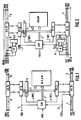
- FIG. 1 is the partial functional block diagram of a first embodiment of the crossing point according to the invention.
- FIG. 2 is the functional block diagram of the first embodiment of the crossing point according to the invention.
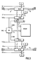
- Fig 3 is the partial functional block diagram of a second embodiment of the crossing point according to the invention.
- FIGS. 4 to 16 relate to parts of the second embodiment of FIG. 3.
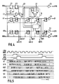
- Figure 4 is the electrical diagram of the first shift register A to B.
- FIG. 5 is a time diagram illustrating the operation of the first shift register of FIG. 4.
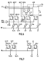
- Figure 6 is the diagram of the first buffer register.
- Figure 7 is the diagram of the second buffer register.
- Figure 8 is the diagram of the second shift register C to D.
- FIG. 9 represents a logic circuit used to generate logic signals to be applied to certain inputs of the circuit of FIG. 8.
- FIG. 10 is a time diagram illustrating the operation of the second shift register of FIG. 8.
- FIG. 11 is a block diagram of the RAM management unit, in conjunction with the buffer registers and the RAM.
- FIG. 12 represents a logic circuit used to generate logic signals internal to the RAM management unit.
- FIG. 13 is an electronic diagram of the control circuit of the RAM represented in FIG. 11.
- FIG. 14 is a time diagram illustrating the operation of the circuit of FIG. 13.
- FIG. 15 is an electronic diagram of the write and read address pointers represented in FIG. 11.
- FIG. 16 is an electronic diagram of the threshold circuit shown in FIG. 11.
- the information propagates on the A-B bus at the rate of the synchronous HBA and HBB clocks, which are supplied to the RAB register.
- the RAB register is arranged in cut-off on bus A-B.
- the bits of the packets enter, leave and shift within the register, in series.
- the order to transfer from the register RAB to MRAM is carried out by means of the logical order TAB in the given low state, on a conductor 1 in the buffer register RTE so that the latter stores , in less than a bit time, the contents of the RAM register and, simultaneously, to the GM management body of MRAM.
- This order results in a command to write the content of the buffer register RTE in MRAM to an address pointing to an empty word location in MRAM.
- This address is carried by an address bus 2 which connects the GM unit to MRAM and which also serves as a read address bus.
- the effective transfer of a packet from the RTE register into MRAM, on a data bus 3, results from a logic signal WE in the low state, coming from the management unit GM, carried by a conductor 4 and which puts at low impedance, output 5 of the RTE register.
- the operation on the CD bus side is similar to that described in the previous paragraph. On this subject, it is It is important to note that the operation of the CD bus is completely independent of the operation of the AB bus both from the point of view of synchronism and of information flow or extraction and insertion decisions, respectively.
- the information propagates on the CD bus at the rate of the synchronous HBC and HBD clocks, which are supplied to the RCD register.
- the RCD register is arranged in cutoff mode on the CD bus. For each packet circulating on the CD bus, the order of transfer of a packet from the buffer register RTS to the shift register RCD is carried out by means of the logical order TCD given, on a conductor 5, both at the GM management body and the RCD shift register.
- the action is not really undertaken and is carried out in parallel in less than a bit time, only when a packet is fully contained in the RCD register.
- the packet insertion order results in a read command imposed by a logic signal TCD in the low state on the storage input of the register RCD.
- a new packet is transferred from MRAM to the RTS buffer register.
- This second transfer takes place from the same logic signal TCD; indeed this second transfer results from a logic signal RE in the low state, coming from the management unit GM on command of the signal TCD in the low state, carried by a conductor 6 and which is applied to the input for memorizing the RTS register.
- MRAM is read in by the address bus 2 and the data flows from MRAM to the RTS register on the data bus 3.
- the memory plane management unit, GM receives logic orders TAB and TCD from conductors 1 and 6 in a completely asynchronous manner.
- the GM unit is designed to resolve conflicts over access to the MRAM memory map over time, more precisely to organize the write and read cycles in MRAM over time. We know that it is not possible to write and read a RAM memory simultaneously. If a read order from MRAM to RTS, following the transfer of the content from RTS to RCD, is present on the driver 6 while MRAM is being written, the reading order in question is memorized, in GM, until the writing order is finished at an instant t5 and does not start until after a time delay initiated in t5.
- the symmetrical operation is identical for an order to write the content of RTE in MRAM arriving during the execution of a read cycle.
- the memorizations and time delays are carried out in GM by means of logic circuits attacked by the HAC clock. It will be noted in this regard that the frequency of the HAC clock is equal to or greater than the highest bit clock frequency HBA or HBC.
- RTE and RTS buffer registers which operate entirely in parallel, have been associated with each serial register.
- the memory MRAM is managed as one or more queues by the management unit GM and, in both cases, each queue ensures the exchange only in the direction from the bus AB to the bus CD. This allows the crossing point to be produced simply from a memory plane and from a management device.
- the use of a random access memory plan, MRAM makes it possible to obtain a maximum memory capacity with equal component area.
- the GM memory plan manager transforms MRAM into one or more queues.
- the access time to the memory plane is the critical element of the crossing point, the length of the words is as large as possible. So for the same number of switched bits given, the number of accesses will be inversely proportional to the length of the word. Under these conditions, the preferred word length is the length of a packet.
- the memory locations of MRAM are thus used cyclically by the two pointers, the read pointer naturally having to be behind the write pointer. Prohibitions can result from a blocking configuration such as: full MRAM during a write request or, conversely, empty MRAM during a read request.
- the GM management body may include a device for measuring the filling rate which permanently receives the addresses of the address pointers for writing and reading. , which establishes the difference between these addresses and which generates a write inhibit, respectively read, signal when MRAM is full, respectively empty.
- the purpose of the crosspoint multiplexing function according to the invention is to mix with the packet flow arriving on bus C, the packet flow from the MRAM queue. The resulting flow leaves at D.
- the implementation of the multiplexing carried out exploits the peculiarity that the ATD packets have, of being of constant and consecutive length. In the absence of information there are packets whose information field is meaningless.
- the multiplexing process is very simple and consists simply of the serial register RCD between the buses C and D with a parallel input from the queue and which has the length of a packet. Multiplexing consists, when the RCD register contains exactly one empty packet, of overwriting it with the packet which is at the head of the queue, more precisely the packet which is preloaded in the RTS buffer register.
- the aforementioned multiplexing method, implemented by the crossing point according to the invention is very easy to integrate and allows high bit rates.
- the MRAM memory can be organized for example as two queues in order to make the second queue totally or partially priority over the first.
- the second queue is then the one that is emptied first, for total priority.
- the person skilled in the art ensures that, for example, the second queue is emptied first but for a limited time after which the first queue can empty itself.
- the equipment for the connection of this subscriber to a bus of the network requires two crossing points operating one in the direction of reception (from bus AB to the CD bus), the other in the direction of transmission (from the CD bus to the AB bus), which results in a change of the start and end buses for packet switching.
- Bus A-B and C-D can be comparable or very different and can be counted in Mbits / s on one bus and in kbits / s on the other bus.
- the shift register RCD is necessarily cut off on the arrival bus, as the information arrival register from another information bus, it is not the same. of the RAB register on the departure bus, whose cut-off position is not essential.
- the RAB register could be arranged as a bypass with respect to the bus A-B, which would have the advantage of saving, on the bus A-B, the filling time of the RAB register for the propagation time of the packets.
- the crossing point of FIG. 1 is preferably produced in the form of a single integrated circuit element, in CMOS technology.
- this element has 75 input outputs, including 64 for connection to buses A, B, C and D.
- each packet is the label of each packet on the bus A, respectively on the bus C, which carries the information necessary for the extraction, respectively the insertion of the packet.
- the clock wires HEAB, HPA and HBA are connected to the packet extraction decision device DE as well as the conductor (s) of bus A which is (are) relative ( s) the label field.
- the clock HPA determines, in DE, the instant t2 at which the entire packet coming from the bus A (useful information plus label) is in the register RAB.
- the clock HEAB determines, in DE, the instant t1 at which the member DE received the entire label of each packet. It will be noted that the label is arranged, chronologically speaking, at the head of each packet, which amounts to saying that the instant t1 precedes the instant t2.
- the duration t2-t1 is used to make the decision to extract or not extract the packet contained in the RAB register at time t2 and to carry out this transfer, in the event of an extraction decision, in less than a clock period HBA, from the RAM register in parallel to the buffer register RTE.
- HBA clock period
- the DE organ when the DE organ has received the entire label, it is able, on the basis of the content of the label and depending on its internal logic, to take one of the following two decisions: either in in a first case, the packet must be copied from the RAB register to the MRAM memory plan, or in a second case, the packet must not be copied in the MRAM memory plan.
- This order, whether or not to copy each packet is supplied by the member DE to the driver 1; it constitutes the logical order TAB of FIG. 1.
- the HECD, HPC and HBC clock wires are connected to the insertion decision member of DI packets as well as the bus conductor (s) which is (are) relative to the label field.
- the clock HPC determines in DI, the instant t4 at which the entire packet coming from the bus C (useful information plus label) is in the register RCD.
- the clock HECD determines, in DI, the instant t3 at which the member DI has received the entire label of each packet.
- the label is placed at the head of each packet, which implies that t3 is earlier than t4.
- the duration t4-t3 is used to make the decision to insert or not insert a packet, from the RTS register which contains it, into the RCD register at time t l'instant and to carry out this transfer, in the event decision to insert, in less than one HBC clock period, from the RTS register, in parallel, to the RCD register.
- the DI body when the DI body has received the entire label, it is able, on the basis of the content of the label and according to its internal logic, to take one of the following two decisions: either in a first case, the packet coming from bus C which carries this label is a non-empty packet and in this case the decision is not to make an insertion and to let the packet contained in the RCD register go out on bus D ; or in a second case, the packet coming from bus C is empty, that is to say that its information field is meaningless and in this case the decision taken between times t3 and t4 will be to copy the packet which is in the RTS register, coming from the MRAM memory plane, in the RCD register and therefore overwriting the empty packet therein.
- the packet entering bus C is empty is not necessarily sufficient to overwrite it in the RCD register; the insertion decision-making body DI can in fact take account of other information contained in the label of the package to decide whether or not to overwrite the package.
- the order to copy or not the RTS packet to RCD is provided by the DI member to driver 6; it constitutes the logical order TCD of FIG. 1.
- the packet extraction or insertion decision logic consists of the DE, TEX blocks, and the DI, TIN blocks respectively. It is this logic that makes the decision to transfer from an AB bus (or CD) to the other CD (or AB).
- This logic is fully distributed, that is to say that not only is it associated with each crossing point and independent of that of the others, but it also consists of two independent devices for the AB bus and the CD bus. Both devices use the same hardware solution and are fully programmable.
- the decision logic is associated not only with each crossing point but also with each bus whose distances to be covered by the decision signals are negligible and the decisions relate only to the packets of the bus AB or of the bus CD and do not depend on any decision from another crossing point. In principle, all the information necessary for the decision is conveyed with the package itself in a field of the label.
- the value 0 or 1 of the bit addressed corresponds to the decision whether or not to store this packet in memory, respectively to replace it or not with a packet from MRAM memory.
- the member DE is connected to the TEX table by an address bus with n conductors, 8.
- the label of each packet on the bus A is transmitted to the bus 8.
- the TEX decision table comprises 2 n locations, addressed by bus 8 and whose content is pre-programmed to 0 or 1.
- the content of the location addressed by bus 8 is transmitted from TEX to DE by a driver 9. This last information, possibly supplemented by information coming from the outside, not shown, is translated into DE by a command for extracting or not extracting a packet from the register RAB.
- the DI and TIN organs have a structure and function identical to DE and TEX; they are interconnected by bus 11, counterpart of 8, and conductor 12, counterpart of 9.
- the registers E, F, G, and H are for example filled, in a manner not shown, by a synchronous serial interface; their outputs, in parallel, are connected to parallel label inputs, by multiple switches, switch 15 for E to the register RAB under the control of a logic signal CE, switch 16 for F to the register RTE under the control of the logic signal CF, the switch 17 for G to the register RCD under the control of the logic signal CG and the switch 18 for H to the register RCD under the control of the logic signal CH.
- a usefulness of the label change is for example the following, with regard to the label register E: it can be decided that when a packet is extracted from the register RAB intended for the bus CD, it is no longer useful on the departure bus AB although it continues on this bus.
- the register E is then used, on the occasion of the passage of this packet in the register RAB, to transform its label into a label of free packet, that is to say of empty packet, whose useful information field, henceforth meaningless, can be overwritten later.
- this modification of label on the departure bus AB is only possible with a shift register RAB arranged in cut-off on this departure bus, which is still the case in this third embodiment.
- the length of the RAB register corresponds at least to that of a packet. When RAB contains a packet, the latter can, by external decision, be transferred to MRAM with or without modification of its label depending on the value of the logic signal CF.
- the RCD output register is cut off on the CD bus. Its length also corresponds at least to that of a package.
- RCD contains a packet
- the latter can, by external decision, be replaced by a packet coming from MRAM with or without modification of its label according to the value of the logic signal CH.
- the packets circulating on the buses AB and CD can, by external decision, have their labels modified under the control of the logic signals CE and CG respectively.
- the data is carried for example by 16 conductors in parallel which constitute the buses A, B, C and D, these conductors being referenced by A1 to A16; B1 to B16; C1 to C16 and D1 to D16.
- the general operation of the crossing point in Figure 3 is as follows:
- the data relating to a packet, P enters the first series-parallel shift register RAB.
- the packet P When the packet P is contained in its entirety in AB it can be transferred into the first input buffer register RTE, in less than a bit time, entirely in parallel, either on 272 conductors simultaneously, with or without modification of its label , under the control of the logic signal TAB.
- the MRAM queue is produced by a RAM memory whose access time is greater than an HBA clock period; on the other hand we know that we cannot read and write at the same time in RAM. If MRAM is not available when the P packet is transferred to RTE, i.e. if MRAM is in the read cycle, the P packet remains stored in RTE and the write request in MRAM is also stored, in GM. When MRAM remains free, the write cycle takes place. The packet P contained in RTE is then put on the data bus 3 of MRAM. Note that the storage time of a packet in RTE is at most equal to 17 HBA clock periods, ie the time for a packet contained in RAB to be replaced by the next packet.
- the data on the bus C enters the second parallel-serial shift register RCD.
- RCD the second parallel-serial shift register
- a packet is contained in its entirety in RCD it can be replaced by the packet contained in the second output buffer register RTS, in less than a bit time, entirely in parallel, ie on 272 conductors simultaneously, with or without modification of its label, under the control of the logic signal TCD.
- MRAM is read to reload RTS. Otherwise, the read request is stored in GM and made as soon as possible.
- the new loading of RTS is always carried out in a time less than the time of replacement of a packet by the next packet in RCD; for an HBC clock at 128 kHz, this replacement time is equal to 132.6 e s.
- the management unit GM manages the address bus 2 of MRAM, in read cycle and in write cycle, to operate this RAM as a queue. It is also this part of the component which preferably provides instant information on the filling of MRAM.
- the first shift register RAB which comprises 16 serial inputs connected to A1-A16, the inputs relating to A1 and A16 alone being shown.
- the clock signals HBA, HPA and the logic control signal CE are also supplied.
- the output of the register RAB comprises 18 signals, which are: the data intended for B1 to B16, the clock associated with the data B, HPB, and the synchronization signal of the packets received on the bus B, HBB.
- the RAB register consists of 16 identical sub-registers for each data wire A1 to A16. Each sub-register consists of 19 D-FF flip-flops in cascade referenced 1-1, ..., 1-19; ...; 16-1, ..., 16-19.
- the first 18 flip-flops are triggered on the rising edge of HBA, on their increment input, to produce an 18-bit shift register.
- the nineteenth flip-flop is triggered on the falling edge of HBA, by means of the inverter 17 so that the output signal on B1 to B16 is in phase with the input signal on A1 to A16.
- the data changes state on the falling edge of the associated clock, HBA and HBB which are identical, as shown in FIG. 5 for A1, A16, B1, B16.
- the synchronization signal HPA goes high for the duration of transmission of the 16 label bits, that is to say for the duration of a clock period HBA since the data are in parallel on 16 wires .
- an AND gate circuit 18 which receives the signals HPA and CE and whose output signal CP as well as its complement CP are transmitted to a logic circuit with three NAND gates, 19 for each sub-register.
- the logic circuit 19 also receives the signal from the output Q of the seventeenth flip-flop D of the corresponding sub-register as well as the output signal, corresponding to the sequence number of the associated sub-register, from the label register E.
- the output of circuit 19 is connected to input D of the eighteenth scale.
- the function performed by circuit 19 is equivalent to that of a two-position switch: (Q1. CP ⁇ ) + (E1.CP)
- the label is modified when the CE and HPA signals are simultaneously in the high state, which is supposed to be the case in FIG. 5.
- the eighteenth flip-flop of the 16 shift registers can be preloaded with the contents of the E register of to modify the label of a frame of a packet. This preloading is carried out by putting the content of the register E on the inputs of the 16 flip-flops during the duration of the signal HPAV in the high state, provided that the signal CE is also in the high state during this time.
- the data on B1 to B16 and the signal HPB are equal respectively to the data received on A1 to A16 and to the signal HPA delayed by a time T, as indicated by R1, R16 , in FIG. 5, which constitutes the original label of the packet R.
- the value of T is taken equal to 18 clock periods HBA.
- FIG. 6 represents the first buffer register or input buffer register RTE.
- the signals AB1 to AB16 are replaced by the label contained in F1 to F16 if the signal CF is in the low state.
- 16 devices with three NAND gate circuits 25 allow the choice between the signals on AB1 to AB16 or the signals on F1 to F16, on the inputs of flip-flops RTE1 to RTE16, as a function of the high, respectively low, state of the signal CF. It will be noted in this regard that there is no provision for a packet transfer request by TAB with the signal CF in the high state and a simultaneous request for modification of the label of the packet contained in the register RAB by the signal THIS.
- CE and CF signals are designed so as not to cause label conflicts.
- the outputs TE1 to TE272 of flip-flops D are put on the bus D1 to D272, that is to say the data bus 3 of MRAM during the low state of WE.
- WE is a write command, initiated by the signal TAB, coming from the GM unit and which acts on output 5 of RTE by 3-state control effect, in this case by setting to low impedance .
- the buffer register RTS represented in FIG. 7 is a parallel-parallel register of 272 bits, constituted by 272 flip-flops D RTS1 to RTS272 whose inputs D are connected to the data bus 3 of MRAM, D1 to D272 and the outputs Q referenced TS1 to TS272 are connected to the RCD output register.
- the data coming from MRAM are stored in RTS on the falling edge of the logic signal RE, command to read MRAM produced by the GM organ on the conductor 7.
- the RE signal is initiated in the GM organ from the signal TCD and acts on the increment inputs of flip-flops D of the RTS register.
- the second shift register RCD is shown in Figure 8; it has d parallel inputs connected to the outputs of RTS and referenced in the same way, TS1 to TS257.
- the parallel entries are distributed in groups of 16 into 16 under identical registers of which only two, the first and the last are represented.
- Each sub-register receives a serial input from the bus C, such as C1, C16, and includes a serial output on the bus D, such as D1, D16.
- the clock signals HBC and HPC are also supplied, the connections and the resulting clock signals generated HBD and HPD being analogous and comparable to what is described above with reference to FIGS.
- the logic signal and its complement which are transmitted at the input of the circuits 27 are the signals K2 and K1 obtained by the logic circuit in Figure 9 (AND gate circuit 31 and inverter 32):
- the choice of the n label bits, coming from the bus C, from the register RTS, from the register H or from the register G, is made by means of the logic circuits with five NAND gates 29 which receive the signals K3, K4, K5, K6 generated by the logic circuit of figure 9 from the logic signals: HPC, TCD, CH, CG.
- the data changes state on the falling edge of the associated clock as shown in the time diagram in FIG. 10 where the information bits are identified only by their serial numbers except with regard to the bits coming from RTS whose sequence number is preceded by the letters TS.
- the synchronization signal goes high during the 16 bits of the label. It therefore lasts in this case an HBC clock period since the data are in parallel on 16 wires.
- the data D1 to D16 on the bus D and the signal HPD are equal to the data C1 to C16 received from the bus C and to the signal HPC delayed by a time T '.
- the value of T ' is taken equal to 18 HBC clock periods. Indeed it is necessary to synchronize HPD on HBD.
- the 17 flip-flops k-2 to k-18 (k varying from 1 to 16) of the 16 shift registers can be preloaded by the content of the output buffer register RTS, so as to carry out a transfer of a packet contained in MRAM in the RCD arrival register. This preloading is carried out by putting the content of the register RTS on the inputs of the 272 flip-flops D for the duration of the signal PTCD in the high state, coming from HPC, provided that the logic of the transfer allows it.
- the last flip-flop 1-18 to 16-18 of the 16 shift registers can be preloaded by the content of the registers G or H so as to modify the label of a packet.
- This loading is carried out in an identical manner to that described in the previous paragraph depending on the decision logic chosen.
- This decision logic is for example that which is indicated in the following table I, in which the sign * symbolizes an indifferent logical state, 1 or 0.
- TABLE I ACTION Logic function HPC TCD CH CG Data No transfer K1 condition K2 not fulfilled MRAM transfer K2 1 1 * * Label No transfer K3 conditions K4, K5, or K6 not fulfilled.
- K3, K4, K5 and K6 are realized by the logic circuit of figure 9 (AND gate circuits 31, 33, NOR-OR 34 for K3, AND circuits 31 and 33 for K4, inverters 35 and 36, circuit AND 31 and circuit AND 37 for K5 and circuit AND 38 for K6).
- K4 HPC.TCD.CH
- FIG. 11 represents in the form of a block diagram the GM management organ of MRAM and the figures which follow 12 to 16 represent parts of the GM organ or serve to explain the operation of these parts.
- the MRAM memory is managed as a queue.
- the control block 41 determines the write and read cycles as a function of the packet transfers from RAB to MRAM and from MRAM to RCD. It also indicates whether MRAM is empty or full.
- the write address pointer 43 gives the memory box where the packet contained in RAB then RTE must be written in MRAM. It is incremented after each reading.
- the read address pointer 44 gives the memory box where the packet must be read in order to be written in RTS then RCD. It is incremented after each reading.
- the threshold circuit 45 supplies the signal SMRAM which indicates whether MRAM is fulfilled above a predetermined threshold contained in a register J not shown, for example contained in the circuit 45.
- the filling rate block 42 first contains a register comparator, not shown, which receives the bits AW1-AW8 and the bits AR1-AR8 and thus compares the contents of the write and read address pointers 43 and 44.
- This comparator of a known type, could for example be constituted by the association of several digital integrated circuits C-MOS, of the HEF4585B type, 4-bit number comparator, produced by the company Philips.
- the filling ratio block 42 also contains the logic circuit of FIG.
- the logic circuit of FIG. 12 comprises two OR-exclusive gate circuits 49 and 51, two inverters 52 and 53, and two AND gate circuits 54 and 55 which respectively provide the MRAMP and MRAMV signals at their output.
- Circuit 49 receives signals PFE and PFL
- circuit 54 receives the output signal from circuits 49 and 51 and circuit 55 receives the inverted output signal from circuit 49 and the signal AW> AR reversed.
- the control block 41 is shown in more detail in Figure 13 and the time diagrams in Figure 16 are used to explain its operation.
- a symmetry of operation for reading or for writing in MRAM corresponds to a symmetry of structure which appears clearly between the top (writing) and the bottom (reading) of FIG. 13.
- the block 41 comprises two inverters 57, 58, a flip-flop D 59 whose output Q is referenced WRQ, an AND circuit 61, an OR circuit 62, a flip-flop D 63 whose output Q generates the signal WE and whose output Q used to reset D flip-flops 64, 65 and 66, and D flip-flops 67 and 68.
- the outputs Q respective of scales 64, 65 and 66 are referenced Q1, Q2 and Q3 respectively, and the outputs Q of flip-flops 67 and 68, RWE and Q5 respectively, Q1, Q2, Q3, RWE and Q5 also designating the logic signals carried by these outputs.
- the flip-flops 59 and 67 are reset to zero by the signal Q5 and the flip-flop 63 by the signal RWE.
- the AND circuit 61 receives the signal WRQ and the inverted signal RRQ, RRQ being the homologous signal of WRQ in reading, and its output is connected to an input of the OR circuit 62 which receives the signal WE on another input.
- the output of circuit 62 is connected to input D of flip-flop 63 which receives on its storage input the clock signal HAC.
- the signals Q1, Q2 and Q3 are looped back to the inputs D of flip-flops 64, 65, 66 respectively.
- the Q output of flip-flop 64 is connected to the storage input of flip-flop 65.
- the signals Q2 and Q3 are supplied to the storage input of flip-flops 66 and 67 respectively.
- the storage input of flip-flops 64 and 68 receives the inverted HAC clock signal.
- the homologous elements which generate the logic signal RE are referenced 107 to 118 and we find the homologous signals RRQ, RRE. The only slight difference between the upper and lower parts of the diagram in FIG. 13 is that the flip-flop 114 is reset to zero from the output Q of flip-flop 118 and not from the output Q of scale 113.
- This circuit arrangement makes it possible to obtain the desired time diagrams described in FIG. 14 where it has been assumed that a read request occurs while a write request is in progress.
- All the logic represented in FIG. 13 is controlled by the HAC clock whose frequency is necessarily greater than or equal to the highest frequency among the HBA and HBC clocks.
- the write address pointer 43 represented in FIG. 15 with its output device 46, is an 8-bit asynchronous counter counting from 0 to 255. It is incremented on each falling edge of WE.
- the bits AW1 to AW8 are set to low impedance and set on the address bus 2, A0-A7 of MRAM during the high state of WE.
- Bit AW9 is the most significant PFE write.
- FIG. 15 also represents the elements 44 and 47.
- the crossing point also includes the MRAM threshold circuit 45 shown in FIG. 16.
- This circuit 45 is not used directly for the operation of the crossing point but indirectly through the network to which this crossing point belongs.
- circuit 45 provides the logic signal SMRAM which is a MRAM loading status information. Via the network, this information can have an influence on the TAB and TCD logic signals.
- the circuit 45 includes the register J, connected by its outputs in parallel J1 to J7 to the inputs P1 to P7 of an up-down counter 71, and 4 NOR-gate circuits 72, 73, 74, 75.
- the circuit 72 receives the signals WE and RE and its output is connected to the data input of the up-down counter 71.
- the signal WE is connected to an input of the circuit 73, a second input of which is connected to the output of the circuit 74.
- the signal RE is connected to an input of circuit 74, a second input of which is connected to the output of circuit 73 and whose output is connected to the up-down counting input of circuit 71.
- Circuit 75 receives the signals MRAMP and MRAMV and its output is connected to the reset input PE of the counter 71.
- the signal MRAMP is also supplied to the input P8 of the circuit 71.
- the register J contains the value supplemented by a threshold S, that is: 128-S, threshold at which one wishes compare the instantaneous content of MRAM.
- the SMRAM signal at the output Q8 of circuit 71 goes from the low state to the high state when MRAM is filled above the threshold S.
- the bit Q8 of the counter therefore indicates when it is at 1 that MRAM is filled above of the threshold S. This is obtained by virtue of the fact that the up-down counter 71 is incremented at each write order, and is decremented at each read order. It will be noted that the addressing of MRAM is on 7 bits while the counter 71 is on 8 bits. When MRAM is empty, counter 71 is immediately preset to the value of: 128-S for bits 1 to 7 and zero for bit 8. When MRAM is full, counter 71 is immediately preset to the value of: 128 -S for bits 1 to 7 and 1 for bit 8.
- the two embodiments are preferably produced in C-MOS technology, in the form of one or two integrated circuit components; when there are two components, they are, for their operation, located a few centimeters from each other, one of them being constituted by the elements DE, TEX, DI, TIN, represented in Figure 2.
Description
L'invention concerne un point de croisement entre deux bus monodirectionnels indépendants l'un de l'autre pour multiplexage ATD d'information numérique constituée de paquets de données de longueur fixe consécutifs véhiculés par lesdits bus, ces paquets comportant un champ d'étiquette de n bits et un champ d'information de i bits n et i étant fixes et tels que ![]()
![]()
Il existe de nombreux procédés et dispositifs pour commuter de l'information d'une ligne à une autre. Les procédés et dispositifs adaptés spécialement à la commutation de paquets ATD (Asynchronous Time Division en langue anglaise) sont beaucoup moins nombreux en raison de la nouveauté du concept ATD de multiplexage de l'information. Le multiplexage ATD de l'information fait actuellement l'objet d'une contribution au niveau du CCITT en vue d'une normalisation et peut être caractérisé en ce que l'information est découpée en paquets de longueur fixe, une étiquette de longueur fixe étant associée à chaque paquet et permettant d'identifier la communication à laquelle appartient chaque paquet. Sur la ligne de transmission les paquets sont consécutifs, c'est-à-dire qu'en l'absence d'information, la ligne véhicule des paquets vides (de même longueur que les autres), ne contenant aucune information mais munis chacun d'une étiquette, pour assurer le remplissage. La technique ATD a comme but principal d'atteindre les débits les plus élevés possible ; ceci introduit le problème des temps de propagation des signaux, qui n'est pas négligeable lorsqu'on souhaite conserver une synchronisation correcte entre les signaux porteurs d'information, leurs signaux d'horloge respectifs et les signaux de décision logique.There are many methods and devices for switching information from one line to another. The methods and devices specially adapted to the switching of ATD (Asynchronous Time Division in English) packets are much less numerous because of the novelty of the ATD concept of information multiplexing. ATD multiplexing of information is currently the subject of a contribution at the CCITT level with a view to standardization and can be characterized in that the information is divided into packets of fixed length, a label of fixed length being associated with each packet and making it possible to identify the communication to which each packet belongs. On the transmission line the packets are consecutive, that is to say that in the absence of information, the line carries empty packets (of the same length as the others), containing no information but each provided with 'a label, to ensure filling. The main goal of the ATD technique is to achieve the highest possible throughputs; this introduces the problem of signal propagation times, which is not negligible when it is desired to maintain correct synchronization between the information-carrying signals, their respective clock signals and the logic decision signals.
Le problème technique précis que se propose de résoudre l'invention est de pouvoir commuter les paquets d'information définis ci-dessus d'une ligne à une autre le plus rapidement possible c'est-à-dire d'un bus de départ à un bus d'arrivée, et ceci en prenant soin de ne pas retarder la propagation de l'information sur les bus de départ et d'arrivée. On notera que les paquets sont prévus d'une assez grande longueur, de l'ordre de 256 bits pour le champ d'information (i = 256) et 16,32 ou 48 bits par exemple pour l'étiquette (n = 16,32 ou 48). Par ailleurs, pour obtenir de hauts débits d'information sur les bus ces derniers sont généralement constitués par plusieurs conducteurs en parallèle, par exemple 16 conducteurs.The precise technical problem which the invention proposes to solve is to be able to switch the information packets defined above from one line to another as quickly as possible, that is to say from a departure bus to an arrival bus, taking care not to delay the propagation of information on the departure and arrival buses. It will be noted that the packets are provided with a fairly large length, of the order of 256 bits for the information field (i = 256) and 16.32 or 48 bits for example for the label (n = 16, 32 or 48). Furthermore, in order to obtain high information rates on the buses, the latter generally consist of several conductors in parallel, for example 16 conductors.
Dans un domaine technique assez éloigné de celui de l'invention, à savoir le domaine des systèmes graphiques numériques il est aussi nécessaire d'obtenir en certains points du système des débits d'information très élevés. On connaît, de la publication "Electronique, Techniques et Industries", N°31 du 17 mars 1986, une mémoire RAM à double réseau, qui permet d'éviter un goulet d'étranglement limitant le débit du système graphique. Cette mémoire RAM comporte deux zones de mémoires sur une seule puce de circuit intégré. La première zone est une mémoire RAM dynamique de 256 K utilisée comme mémoire de visualisation et la deuxième zone est une mémoire RAM statique de 1 K adressée par un compteur intégré sur la puce qui permet un accès en série aux données de pixels. Ces deux zones travaillent indépendamment via des ports d'entrée-sortie séparés, sauf pendant les cycles de transfert au cours desquels les données de la deuxième zone sont transférées entièrement en parallèle de la deuxième à la première zone de mémoire, en moins de 200 ns. La structure de cette mémoire n'est cependant Pas conçue et n'est donc pas apte à transférer de l'information d'un bus à un autre.In a technical field quite distant from that of the invention, namely the field of digital graphics systems, it is also necessary to obtain at certain points in the system very high information rates. We know from the publication "Electronics, Techniques and Industries", N ° 31 of March 17, 1986, a dual network RAM memory, which avoids a bottleneck limiting the throughput of the graphics system. This RAM memory has two memory areas on a single integrated circuit chip. The first zone is a dynamic RAM memory of 256 K used as display memory and the second zone is a static RAM memory of 1 K addressed by a counter integrated on the chip which allows serial access to the pixel data. These two zones work independently via separate input / output ports, except during transfer cycles during which the data of the second zone are transferred entirely in parallel from the second to the first memory zone, in less than 200 ns . The structure of this memory is however not designed and is therefore not suitable for transferring information from one bus to another.
En technique ATD, il est connu, en particulier du document IEEE JOURNAL ON SELECTED AREAS IN COMMUNICATIONS, vol. SAC-5, n°9, décembre 1987, pages 1426-1435, IEEE, New-York, US, de K.I. ENG et al intitulé : "A knockout switch for variable-length packets", un commutateur de paquets ATD permettant des débits d'information élevés.In ATD technique, it is known, in particular from the document IEEE JOURNAL ON SELECTED AREAS IN COMMUNICATIONS, flight. SAC-5, n ° 9, December 1987, pages 1426-1435, IEEE, New-York, US, by KI ENG et al entitled: "A knockout switch for variable-length packets", an ATD packet switch allowing bit rates high information.
Ce commutateur opère entre plus de deux bus ; il nécessite un concentrateur du type dit "knockout" en anglais, ce qui introduit une perte de cellules, et cette publication se rapporte en outre à la commutation de paquets de longueur variable.This switch operates between more than two buses; it requires a concentrator of the type known as "knockout" in English, which introduces cell loss, and this publication also relates to the switching of packets of variable length.
On connaît aussi du document IEEE JOURNAL ON SELECTED AREAS IN COMMUNICATIONS, vol.SAC-5 n°8, octobre 1987, pages 1284-1292, IEEE, New-York, US, de S. NOJIMA et al intitulé : "Integrated services packet network using bus matrix switch", dans un réseau de transmission par paquets un commutateur à matrice de points de croisement de bus à raison d'un point de croisement par paire de bus composée d'un bus d'entrée et d'un bus de sortie. Il est précisé que la longueur d'un paquet peut être variable, ce qui implique des dispositions spécifiques pour la commutation des paquets. Selon cette technique la transmission est unidirectionnelle, du bus d'entrée de la matrice vers le bus de sortie de la matrice pour chaque paire et chaque bus comporte deux éléments en série d'entrée, I-PPU et PPD, respectivement de sortie, SPD, O-PPU.We also know from the document IEEE JOURNAL ON SELECTED AREAS IN COMMUNICATIONS, vol.SAC-5 n ° 8, October 1987, pages 1284-1292, IEEE, New-York, US, by S. NOJIMA et al entitled: "Integrated services packet network using bus matrix switch ", in a packet transmission network a matrix switch of bus crossing points at the rate of one crossing point per bus pair composed of an input bus and a bus exit. It is specified that the length of a packet can be variable, which implies specific provisions for the switching of packets. According to this technique, the transmission is unidirectional, from the input bus of the matrix to the output bus of the matrix for each pair and each bus has two elements in series input, I-PPU and PPD, respectively output, SPD , O-PPU.
Un but de l'invention est de réaliser en circuit(s) intégré(s) un point de croisement pour multiplexage ATD d'information numérique entre deux bus, très rapide, pour permettre un débit d'information élevé.An object of the invention is to provide in integrated circuit (s) a crossover point for ATD multiplexing of digital information between two buses, very fast, to allow a high information rate.
Un autre but est de permettre la réalisation de commutateurs importants à l'aide d'architectures variées utilisant comme éléments de base des points de croisement selon l'invention modulaires rapides entre bus pris par paires, ce qui correspond à un souci d'extensibilité.Another object is to allow the production of large switches using various architectures using as basic elements crossover points according to the invention rapid modular between buses taken in pairs, which corresponds to a concern for scalability.
Ces buts sont atteints grâce au fait que le point de croisement défini au premier paragraphe de la description est remarquable en ce qu'il est constitué par la combinaison de deux blocs fonctionnels de circuit intégré :
- Un premier bloc fonctionnel constitué par la succession en cascade entre l'un desdits bus, dit bus de départ, et l'autre bus, dit bus d'arrivée de :
- a) un premier registre à décalage à entrée(s) série-d sorties parallèles disposé en coupure sur le bus de départ,
- b) un premier registre tampon à d entrées parallèles-d sorties parallèles,
- c) une mémoire RAM à m emplacements de d bits munie d'un bus d'adresses pour les m emplacements,
- d) un deuxième registre tampon à d entrées parallèles-d sorties parallèles ;
- e) un deuxième registre à décalage à d entrées parallèles-sortie(s) série disposé en coupure sur le bus d'arrivée,
- et un deuxième bloc fonctionnel logique de décision de commutation comportant au moins, disposés symétriquement par rapport aux bus de départ et d'arrivée, un organe de décision d'extraction (respectivement d'insertion) de paquet, associé chacun à une table de décision préprogrammée, qui reçoit les données d'étiquette des paquets sur le bus de départ (respectivement sur le bus d'arrivée) et qui pilotent chacun un organe de gestion de la RAM relié à cette dernière par ledit bus d'adresses, l'organe de gestion gérant la RAM comme au moins une file d'attente pour les paquets et recevant à cet effet un signal d'horloge HAC, des conducteurs de synchronisation d'horloge bit, d'horloge étiquette et d'horloge paquet étant prévus, et l'extraction non destructive de paquets du bus de départ ainsi que l'insertion de paquets sur le bus d'arrivée étant effectuées de manière asynchrone l'une par rapport à l'autre.
- A first functional block constituted by the cascade succession between one of said buses, said departure bus, and the other bus, said arrival bus of:
- a) a first shift register with serial input (s) -d parallel outputs arranged in cut-off on the outgoing bus,
- b) a first buffer register with d parallel inputs-d parallel outputs,
- c) a RAM memory at m locations of d bits provided with an address bus for the m locations,
- d) a second buffer register with d parallel inputs-d parallel outputs;
- e) a second shift register with d parallel inputs-serial output (s) arranged in cutoff on the incoming bus,
- and a second switching decision logic functional block comprising at least, arranged symmetrically with respect to the departure and arrival buses, a packet extraction (respectively insertion) decision member, each associated with a decision table preprogrammed, which receives the label data of the packets on the departure bus (respectively on the arrival bus) and which each drive a RAM management device connected to the latter by said address bus, the device management managing RAM as at least one queue for packets and receiving for this purpose a HAC clock signal, bit clock, label clock and packet clock synchronization conductors being provided, and non-destructive extraction of packets from the departure bus as well as the insertion of packets on the arrival bus being performed asynchronously with respect to each other.
La structure du point de croisement défini ci-dessus est originale par ses registres tampons qui permettent d'adapter l'écriture (respectivement la lecture) de mots entiers en parallèle dans une RAM, à de hauts débits d'information sur un bus de départ (respectivement d'arrivée). Cette structure est aussi originale en ce que la RAM est gérée comme une (ou plusieurs) file(s) d'attente et en ce que, toujours pour conserver une vitesse élevée de transfert de l'information, ce transfert a lieu de façon unidirectionnelle à travers le point de croisement.The structure of the crossing point defined above is original by its buffer registers which make it possible to adapt the writing (respectively reading) of whole words in parallel in a RAM, to high information rates on a departure bus. (arrival respectively). This structure is also original in that the RAM is managed as one (or more) queue (s) and in that, always to maintain a high speed of information transfer, this transfer takes place in a unidirectional manner through the crossing point.
La fonctionnalité "point de croisement", constitue une analogie avec les architectures spatiales. En effet, un point de croisement peut être considéré comme un commutateur minimum entre deux bus ou lignes. Cependant, selon la technique ATD, l'information commutée n'est pas constituée par de l'information analogique mais par des paquets numériques de bits d'information. Cette particularité, qu'exploite pleinement le point de croisement selon l'invention, permet de combiner les avantages des architectures spatiales avec ceux des architectures temporelles soit pour recréer des architectures de commutateur connues soit pour créer de nouvelles architectures uniquement possibles par cette combinaison spatiale-temporelle.The "crossing point" functionality is an analogy with spatial architectures. Indeed, a crossing point can be considered as a minimum switch between two buses or lines. However, according to the ATD technique, the switched information is not constituted by analog information but by digital packets of information bits. This feature, which is fully exploited by the crossing point according to the invention, makes it possible to combine the advantages of spatial architectures with those of temporal architectures either to recreate known switch architectures or to create new architectures only possible by this spatial combination. temporal.
L'étiquette est disposée, chronologiquement parlant en tête de chaque paquet, ce qui laisse le temps nécessaire, pendant la durée de chargement du premier (respectivement du deuxième) registre à décalage avec un paquet donné, de prendre, en fonction du contenu de l'étiquette de ce paquet la décision d'extraction ou de non extraction du paquet du bus de départ (respectivement la décision d'écrasement ou de non écrasement du paquet sur le bus d'arrivée). A ce sujet, on notera que les décisions logiques d'extraction ou d'insertion de paquet sont toujours portées par des étiquettes, selon la présente invention, car le temps de décision doit être court par rapport au temps de bit étant donnés les débits élevés recherchés. Pour cette raison, lorsque le point de croisement est réalisé sous la forme de deux circuits distincts comme indiqué ci-dessous, ces derniers doivent être disposés à quelques centimètres l'un de l'autre seulement en vue d'un bon fonctionnement, c'est-à-dire pour ne pas nuire à la synchronisation entre les signaux d'information et les signaux de décision logique fournis notamment à l'organe de gestion de la RAM. De cette façon, les décisions d'extraction ou d'insertion de paquet sont entièrement distribuées sur les points de croisement.The label is arranged chronologically at the head of each packet, which leaves the necessary time, during the loading time of the first (respectively the second) shift register with a given packet, to take, depending on the content of the label of this package the decision to extract or not extract the packet from the departure bus (respectively the decision to overwrite or not to overwrite the packet on the arrival bus). On this subject, it will be noted that the logical decisions of packet extraction or insertion are always carried by labels, according to the present invention, because the decision time must be short compared to the bit time given the high bit rates research. For this reason, when the crossing point is made in the form of two separate circuits as indicated below, these must be arranged a few centimeters from each other only for proper operation, it that is, in order not to harm the synchronization between the information signals and the logic decision signals supplied in particular to the RAM management unit. In this way, the package extraction or insertion decisions are fully distributed on the crossing points.
Selon un mode de réalisation particulier de l'invention, ledit deuxième bloc fonctionnel comporte en outre des registres internes E, F, G, H chargés avec des valeurs d'étiquette, chacun de ces registres comportant des sorties parallèles qui peuvent être commutées par un signal externe sur des(les) entrées parallèles des champs d'étiquette respectivement dudit premier registre à décalage, dudit premier registre tampon, ou dudit deuxième registre à décalage.According to a particular embodiment of the invention, said second functional block further comprises internal registers E, F, G, H loaded with tag values, each of these registers comprising parallel outputs which can be switched by a external signal on (the) parallel inputs of the label fields respectively of said first shift register, said first buffer register, or said second shift register.
Un point de croisement est constitué des deux blocs fonctionnels définis ci-dessus. Ces blocs peuvent être réalisés sous la forme d'un circuit intégré unique ou sous la forme de deux circuits intégrés. Dans les deux cas, le nombre d'entrées-sorties de ces circuits est élevé, surtout pour des bus à 16 conducteurs ou plus, car chacun de ces circuits comporte nécessairement un nombre d'entrées-sorties égal à deux fois le nombre de conducteurs de chaque bus plus d'autres entrées-sorties qui sont précisées ci-dessous. De préférence, le point de croisement est réalisé en technologie C-MOS et ses différentes parties peuvent être conçues sous la forme dynamique et/ou statique. Les registres à décalage, les registres tampon et la RAM du point de croisement sont par exemple conçus pour traiter entièrement en parallèle des paquets dont la longueur est égale ou supérieure à 288 bits. Par exemple, la mémoire RAM comporte 128 ou 256 emplacements de mots de 288 bits ou plus. On notera par ailleurs que les débits d'information sur les bus de départ et d'arrivée peuvent être différents et même très différents.A crossing point consists of the two functional blocks defined above. These blocks can be produced in the form of a single integrated circuit or in the form of two integrated circuits. In both cases, the number of inputs-outputs of these circuits is high, especially for buses with 16 conductors or more, because each of these circuits necessarily has a number of inputs-outputs equal to twice the number of conductors of each bus plus other I / O which are specified below. Preferably, the crossing point is made in C-MOS technology and its different parts can be designed in dynamic form and / or static. The shift registers, the buffer registers and the crossing point RAM are for example designed to process packets whose length is equal to or greater than 288 bits in parallel. For example, the RAM memory has 128 or 256 word locations of 288 bits or more. Note also that the information rates on the departure and arrival buses can be different and even very different.
La description qui suit en regard des dessins annexés, le tout donné à titre d'exemple fera bien comprendre comment l'invention peut être réalisée.The following description with reference to the accompanying drawings, all given by way of example will make it clear how the invention can be implemented.
La figure 1 est le schéma synoptique fonctionnel partiel d'un premier mode de réalisation du point de croisement selon l'invention.FIG. 1 is the partial functional block diagram of a first embodiment of the crossing point according to the invention.
La figure 2 est le schéma synoptique fonctionnel du premier mode de réalisation du point de croisement selon l'invention.FIG. 2 is the functional block diagram of the first embodiment of the crossing point according to the invention.
La figue 3 est le schéma synoptique fonctionnel partiel d'un deuxième mode de réalisation du point de croisement selon l'invention.Fig 3 is the partial functional block diagram of a second embodiment of the crossing point according to the invention.
Les figures 4 à 16 se rapportent à des parties du deuxième mode de réalisation de la figure 3.FIGS. 4 to 16 relate to parts of the second embodiment of FIG. 3.
La figure 4 est le schéma électrique du premier registre à décalage A vers B.Figure 4 is the electrical diagram of the first shift register A to B.
La figure 5 est un diagramme de temps illustrant le fonctionnement du premier registre à décalage de la figure 4.FIG. 5 is a time diagram illustrating the operation of the first shift register of FIG. 4.
La figure 6 est le schéma du premier registre tampon.Figure 6 is the diagram of the first buffer register.
La figure 7 est le schéma du deuxième registre tampon.Figure 7 is the diagram of the second buffer register.
La figure 8 est le schéma du deuxième registre à décalage C vers D.Figure 8 is the diagram of the second shift register C to D.
La figure 9 représente un circuit logique servant à engendrer des signaux logiques à appliquer à certaines entrées du circuit de la figure 8.FIG. 9 represents a logic circuit used to generate logic signals to be applied to certain inputs of the circuit of FIG. 8.
La figure 10 est un diagramme de temps illustrant le fonctionnement du deuxième registre à décalage de la figure 8.FIG. 10 is a time diagram illustrating the operation of the second shift register of FIG. 8.
La figure 11 est un schéma synoptique de l'organe de gestion de la RAM, en liaison avec les registres tampons et la RAM.FIG. 11 is a block diagram of the RAM management unit, in conjunction with the buffer registers and the RAM.
La figure 12 représente un circuit logique servant à engendrer des signaux logiques internes à l'organe de gestion de la RAM.FIG. 12 represents a logic circuit used to generate logic signals internal to the RAM management unit.
La figure 13 est un schéma électronique du bloc-circuit de commande de la RAM représenté sur la figure 11.FIG. 13 is an electronic diagram of the control circuit of the RAM represented in FIG. 11.
La figure 14 est un diagramme de temps illustrant le fonctionnement du circuit de la figure 13.FIG. 14 is a time diagram illustrating the operation of the circuit of FIG. 13.
La figure 15 est un schéma électronique des pointeurs d'adresse écriture et lecture représentés sur la figure 11.FIG. 15 is an electronic diagram of the write and read address pointers represented in FIG. 11.
La figure 16 est un schéma électronique du circuit de seuil représenté sur la figure 11.FIG. 16 is an electronic diagram of the threshold circuit shown in FIG. 11.
Sur la figure 1 on distingue les éléments suivants :
- A-B
- un premier bus monodirectionnel dit bus de départ,
- C-D
- un deuxième bus monodirectionnel dit bus d'arrivée,
- MRAM
- un plan mémoire RAM dont la largeur de mot est égale à celle d'un paquet, soit d bits et qui peut contenir m mots ou emplacements,
- GM
- un organe de gestion de MRAM
- RAB
- un premier registre à décalage A vers B et sortie parallèles vers RTE,
- RTE
- un premier registre tampon entre RAB et MRAM
- RCD
- un deuxième registre à décalage C vers D et entrée parallèle en provenance de RTS,
- RTS
- un deuxième registre tampon entre MRAM et RCD
- HBA
- le fil d'horloge bit du bus A
- HBB
- le fil d'horloge bit du bus B
- HPA
- le fil d'horloge paquet du bus A
- HPB
- le fil d'horloge paquet du bus B
- HBC
- le fil d'horloge bit du bus C
- HBD
- le fil d'horloge bit du bus D
- HPC
- le fil d'horloge paquet du bus C
- HPD
- le fil d'horloge paquet du bus D
- HAC
- l'entrée d'horloge de l'organe de gestion GM
- TAB
- un premier signal de commande logique du registre tampon RTE et de l'organe GM,
- TCD
- un deuxième signal de commande logique du registre à décalage RCD et de l'organe GM,
- AB
- a first unidirectional bus called the departure bus,
- CD
- a second unidirectional bus called the arrival bus,
- MRAM
- a RAM memory map whose word width is equal to that of a packet, ie d bits and which can contain m words or locations,
- GM
- a management body of MRAM
- RAB
- a first shift register A to B and parallel output to RTE,
- RTE
- a first buffer register between RAB and MRAM
- RCD
- a second shift register C to D and parallel input from RTS,
- RTS
- a second buffer register between MRAM and RCD
- HBA
- the bit clock wire of bus A
- HBB
- the bit clock wire of bus B
- HPA
- the packet clock wire of bus A
- HPB
- bus packet clock wire B
- HBC
- the bit clock wire of bus C
- HBD
- the bit clock wire of bus D
- HPC
- the packet clock wire from bus C
- HPD
- the packet clock wire from bus D
- HAC
- the clock input of the GM management body
- TAB
- a first logic control signal from the buffer register RTE and from the unit GM,
- TCD
- a second logic control signal from the shift register RCD and from the unit GM,
L'information se propage sur le bus A-B au rythme des horloges HBA et HBB, synchrones, qui sont fournies au registre RAB. Le registre RAB est disposé en coupure sur le bus A-B. Pour chaque fil du bus A-B (ce bus pouvant au moins en théorie se réduire à un seul fil), les bits des paquets entrent, sortent et se décalent à l'intérieur du registre, en série. Pour chaque paquet circulant sur le bus A-B, l'ordre de transfert du registre RAB vers MRAM s'effectue au moyen de l'ordre logique TAB à l'état bas donné, sur un conducteur 1 au registre tampon RTE pour que ce dernier emmagasine, en moins d'un temps de bit, le contenu du registre RAM et, simultanément, à l'organe de gestion GM de MRAM. Cet ordre se traduit par une commande d'écriture du contenu du registre tampon RTE dans MRAM à une adresse pointant un emplacement de mot vide dans MRAM. Cette adresse est portée par un bus d'adresse 2 qui relie l'organe GM à MRAM et qui sert aussi de bus d'adresse en lecture. Le transfert effectif d'un paquet du registre RTE dans MRAM, sur un bus de données 3, résulte d'un signal logique WE à l'état bas, issu de l'organe de gestion GM, porté par un conducteur 4 et qui met en basse impédance la sortie 5 du registre RTE.The information propagates on the A-B bus at the rate of the synchronous HBA and HBB clocks, which are supplied to the RAB register. The RAB register is arranged in cut-off on bus A-B. For each wire of bus A-B (this bus can at least be reduced to a single wire in theory), the bits of the packets enter, leave and shift within the register, in series. For each packet circulating on the bus AB, the order to transfer from the register RAB to MRAM is carried out by means of the logical order TAB in the given low state, on a
Le fonctionnement du côté du bus C-D est analogue à ce qui est décrit au paragraphe précédent. A ce sujet, il est important de noter que le fonctionnement du bus C-D est totalement indépendant du fonctionnement du bus A-B tant au point de vue du synchronisme que du débit de l'information ou des décisions d'extraction, respectivement d'insertion. L'information se propage sur le bus C-D au rythme des horloges HBC et HBD, synchrones, qui sont fournies au registre RCD. Le registre RCD est disposé en coupure sur le bus C-D. Pour chaque paquet circulant sur le bus C-D, l'ordre de transfert d'un paquet du registre tampon RTS vers le registre à décalage RCD s'effectue au moyen de l'ordre logique TCD donné, sur un conducteur 5, à la fois à l'organe de gestion GM et au registre à décalage RCD. L'action n'est réellement entreprise et s'effectue en parallèle en moins d'un temps de bit, que lorsqu'un paquet est contenu intégralement dans le registre RCD. L'ordre d'insertion de paquet se traduit par une commande de lecture imposée par un(le) signal logique TCD à l'état bas sur l'entrée de mémorisation du registre RCD. Juste après ce transfert un nouveau paquet est transféré de MRAM dans le registre tampon RTS. Ce deuxième transfert s'effectue à partir du même signal logique TCD ; en effet ce deuxième transfert résulte d'un signal logique RE à l'état bas, issu de l'organe de gestion GM sur commande du signal TCD à l'état bas, porté par un conducteur 6 et qui est appliqué à l'entrée de mémorisation du registre RTS. Pendant le deuxième transfert, MRAM est adressée en lecture par le bus d'adresses 2 et les données circulent de MRAM au registre RTS sur le bus de données 3.The operation on the CD bus side is similar to that described in the previous paragraph. On this subject, it is It is important to note that the operation of the CD bus is completely independent of the operation of the AB bus both from the point of view of synchronism and of information flow or extraction and insertion decisions, respectively. The information propagates on the CD bus at the rate of the synchronous HBC and HBD clocks, which are supplied to the RCD register. The RCD register is arranged in cutoff mode on the CD bus. For each packet circulating on the CD bus, the order of transfer of a packet from the buffer register RTS to the shift register RCD is carried out by means of the logical order TCD given, on a
L'organe de gestion du plan mémoire, GM, reçoit des ordres logiques TAB et TCD en provenance des conducteurs 1 et 6 d'une manière totalement asynchrone. L'organe GM est conçu pour régler dans le temps les conflits d'accès au plan mémoire MRAM, plus précisément pour organiser dans le temps les cycles d'écriture et de lecture dans MRAM. On sait en effet qu'il n'est pas possible d'inscrire et de lire simultanément une mémoire RAM. Si un ordre de lecture de MRAM vers RTS, consécutif au transfert du contenu de RTS dans RCD, est présent sur le conducteur 6 alors que MRAM est en cours d'inscription, l'ordre de lecture en question est mémorisé, en GM, jusqu'à ce que l'ordre d'écriture soit terminé à un instant t₅ et ne commence qu'après une temporisation initiée en t₅. Le fonctionnement, symétrique, est identique pour un ordre d'écriture du contenu de RTE dans MRAM arrivant pendant l'exécution d'un cycle de lecture. Les mémorisations et temporisations sont effectuées en GM au moyen de circuits logiques attaqués par l'horloge HAC. On notera à ce sujet que la fréquence de l'horloge HAC est égale ou supérieure à la plus haute fréquence d'horloge bit HBA ou HBC. Outre le règlement des conflits écriture/lecture dans MRAM, pour assurer l'asynchronisme entre les registres série RAB et RCD qui fonctionnent sur une horloge bit HBA et HBC et la mémoire MRAM qui fonctionne au rythme d'une horloge paquet HPAB ou HPCD, les registres tampons RTE et RTS, qui fonctionnent entièrement en parallèle, ont été associés à chaque registre série. De plus, ils permettent l'isolement entre le bus d'adresses du plan mémoire et les accès parallèles des bus série ; autrement dit, les transferts en parallèle en moins d'un temps de bit du contenu du registre RAM vers MRAM et d'un mot issu de MRAM vers le registre RCD sont ainsi rendus possibles, et compatibles avec les cycles d'écriture et de lecture de MRAM à partir du même bus d'adresse 2.The memory plane management unit, GM, receives logic orders TAB and TCD from
La mémoire MRAM est gérée comme une ou plusieurs files d'attente par l'organe de gestion GM et, dans les deux cas, chaque file d'attente n'assure l'échange que dans le sens du bus A-B vers le bus C-D. Ceci permet de réaliser simplement le point de croisement à partir d'un plan mémoire et d'un organe de gestion. L'utilisation d'un plan mémoire à accès aléatoire, MRAM, permet d'obtenir une capacité de mémoire maximale à surface de composant égale. L'organe de gestion du plan mémoire GM transforme MRAM en une ou plusieurs files d'attente. D'autre part, comme le temps d'accès au plan mémoire est l'élément critique du point de croisement, la longueur des mots est la plus grande possible. Ainsi, pour un même nombre de bits commutés donné, le nombre d'accès sera inversement proportionnel à la longueur du mot. Dans ces conditions, la longueur de mot préférée est la longueur d'un paquet. Le fait que la file d'attente n'assure des échanges que dans un seul sens correspond au fonctionnement le plus courant prévu pour le point de croisement. Cette disposition simplifie plusieurs points critiques de la réalisation, à savoir : en premier lieu, le temps d'accès au plan mémoire est limité et ce temps serait double si l'on devait introduire des files d'attente avec des sens opposés, en second lieu la puissance consommée par l'accès au plan mémoire est ainsi réduite. Ce sens unique de la file d'attente simplifie la réalisation des registres tampons et des registres série, ce qui facilite l'intégration et accroît la vitesse de fonctionnement. On notera que lorsque, dans le cas préféré, MRAM ne comporte qu'une file d'attente, cette mémoire est organisée comme une FIFO. A cet effet, les adresses en écriture et en lecture sont, par exemple engendrées respectivement par des pointeurs d'adresses, c'est-à-dire par des compteurs qui sont incrémentés d'une unité après chaque écriture, respectivement chaque lecture dans la RAM. Les emplacements mémoire de MRAM sont ainsi exploités de façon cyclique par les deux pointeurs, le pointeur en lecture devant naturellement être en retard sur le pointeur en écriture. Des interdictions peuvent résulter d'une configuration de blocage telle que : MRAM pleine lors d'une demande d'écriture ou, à l'inverse, MRAM vide lors d'une demande de lecture. Dans ces deux cas, l'ordre ne doit pas être exécuté et dans ce but, l'organe de gestion GM peut comporter un dispositif de mesure du taux de remplissage qui reçoit en permanence les adresses des pointeurs d'adresse en écriture et en lecture, qui établit la différence entre ces adresses et qui engendre un signal d'inhibition d'écriture, respectivement de lecture, lorsque MRAM est pleine, respectivement vide.The memory MRAM is managed as one or more queues by the management unit GM and, in both cases, each queue ensures the exchange only in the direction from the bus AB to the bus CD. This allows the crossing point to be produced simply from a memory plane and from a management device. The use of a random access memory plan, MRAM, makes it possible to obtain a maximum memory capacity with equal component area. The GM memory plan manager transforms MRAM into one or more queues. On the other hand, as the access time to the memory plane is the critical element of the crossing point, the length of the words is as large as possible. So for the same number of switched bits given, the number of accesses will be inversely proportional to the length of the word. Under these conditions, the preferred word length is the length of a packet. The fact that the queue only carries out exchanges in one direction corresponds to the most common operation planned for the crossing point. This arrangement simplifies several critical points of the realization, namely: firstly, the access time to the memory plane is limited and this time would be double if one had to introduce queues with opposite directions, secondly place the power consumed by access to the memory plane is thus reduced. This unique direction of the queue simplifies the creation of buffer registers and serial registers, which facilitates integration and increases operating speed. Note that when, in the preferred case, MRAM has only one queue, this memory is organized like a FIFO. For this purpose, the write and read addresses are, for example generated respectively by address pointers, that is to say by counters which are incremented by one after each write, respectively each read in the RAM. The memory locations of MRAM are thus used cyclically by the two pointers, the read pointer naturally having to be behind the write pointer. Prohibitions can result from a blocking configuration such as: full MRAM during a write request or, conversely, empty MRAM during a read request. In these two cases, the order must not be executed and for this purpose, the GM management body may include a device for measuring the filling rate which permanently receives the addresses of the address pointers for writing and reading. , which establishes the difference between these addresses and which generates a write inhibit, respectively read, signal when MRAM is full, respectively empty.
La fonction de multiplexage du point de croisement selon l'invention a pour objet de mélanger au flux de paquet qui arrive sur le bus C, le flux de paquet en provenance de la file d'attente de MRAM. Le flux résultant sort en D. La mise en oeuvre du multiplexage réalisé exploite la particularité qu'ont les paquets ATD, d'être de longueur constante et consécutifs. En l'absence d'information il y a des paquets dont le champ information est sans signification. Le procédé de multiplexage est très simple et consiste simplement en le registre série RCD entre les bus C et D avec une entrée parallèle depuis la file d'attente et qui a la longueur d'un paquet. Le multiplexage consiste, au moment où le registre RCD contient exactement un paquet vide, à l'écraser par le paquet qui se trouve en tête de la file d'attente, plus précisément le paquet qui se trouve préchargé dans le registre tampon RTS. Comme ce remplacement se fait totalement à l'intérieur du registre RCD, il n'y a aucun conflit d'accès au bus C-D avec un autre point de croisement. En raison de sa grande simplicité de conception, la méthode de multiplexage précitée, mise en oeuvre par le point de croisement selon l'invention est très facile à intégrer et permet des débits élevés.The purpose of the crosspoint multiplexing function according to the invention is to mix with the packet flow arriving on bus C, the packet flow from the MRAM queue. The resulting flow leaves at D. The implementation of the multiplexing carried out exploits the peculiarity that the ATD packets have, of being of constant and consecutive length. In the absence of information there are packets whose information field is meaningless. The multiplexing process is very simple and consists simply of the serial register RCD between the buses C and D with a parallel input from the queue and which has the length of a packet. Multiplexing consists, when the RCD register contains exactly one empty packet, of overwriting it with the packet which is at the head of the queue, more precisely the packet which is preloaded in the RTS buffer register. As this replacement is done entirely inside the RCD register, there is no conflict of access to the CD bus with another crossing point. Because of its great simplicity of design, the aforementioned multiplexing method, implemented by the crossing point according to the invention is very easy to integrate and allows high bit rates.
La logique de décision d'extraction ou d'insertion de paquet est totalement distribuée comme décrit ci-dessous en référence à la figure 2.The packet extraction or insertion decision logic is fully distributed as described below with reference to Figure 2.
La mémoire MRAM peut être organisée par exemple comme deux files d'attente dans le but de rendre prioritaire totalement ou partiellement la deuxième file d'attente par rapport à la première. La deuxième file d'attente est alors celle qui est vidée la première, pour une priorité totale. Pour une priorité partielle correspondant à une logique mixte, l'homme de l'art fait en sorte que, par exemple, la deuxième file d'attente se vide d'abord mais pendant un temps limité après lequel la première file d'attente peut se vider à son tour. Pour un abonné qui souhaite à la fois pouvoir émettre ou recevoir de l'information, l'équipement pour la connexion de cet abonné à un bus du réseau nécessite deux points de croisement fonctionnant l'un dans la direction de la réception (du bus A-B vers le bus C-D), l'autre dans la direction de l'émission (du bus C-D vers le bus A-B), ce qui se traduit par une permutation des bus de départ et d'arrivée pour la commutation des paquets.The MRAM memory can be organized for example as two queues in order to make the second queue totally or partially priority over the first. The second queue is then the one that is emptied first, for total priority. For a partial priority corresponding to a mixed logic, the person skilled in the art ensures that, for example, the second queue is emptied first but for a limited time after which the first queue can empty itself. For a subscriber who wishes at the same time to be able to transmit or receive information, the equipment for the connection of this subscriber to a bus of the network requires two crossing points operating one in the direction of reception (from bus AB to the CD bus), the other in the direction of transmission (from the CD bus to the AB bus), which results in a change of the start and end buses for packet switching.
Les débits d'information sur les bus A-B et C-D peuvent être comparables ou bien très différents et se compter en Mbits/s sur un bus et en kbits/s sur l'autre bus.Information rates on buses A-B and C-D can be comparable or very different and can be counted in Mbits / s on one bus and in kbits / s on the other bus.
On notera aussi que si le registre à décalage RCD est nécessairement en coupure sur le bus d'arrivée, en tant que registre d'arrivée d'information en provenance d'un autre bus d'information, il n'en est pas de même du registre RAB sur le bus de départ, dont la position en coupure n'est pas indispensable. En effet, le registre RAB pourraît être disposé en dérivation par rapport au bus A-B, ce qui aurait l'avantage d'économiser, sur le bus A-B, le temps de remplissage du registre RAB pour le temps de propagation des paquets. Cependant, on préfère, selon la présente invention, conserver le registre à décalage en coupure sur le bus de départ, pour une meilleure régénération des signaux et une bonne resynchronisation de ces signaux avec leur horloge bit. Un autre avantage qui apparaît sur la figure est de conserver au composant une certaine symétrie.It will also be noted that if the shift register RCD is necessarily cut off on the arrival bus, as the information arrival register from another information bus, it is not the same. of the RAB register on the departure bus, whose cut-off position is not essential. In fact, the RAB register could be arranged as a bypass with respect to the bus A-B, which would have the advantage of saving, on the bus A-B, the filling time of the RAB register for the propagation time of the packets. However, it is preferred, according to the present invention, to keep the cut-off shift register on the start bus, for better regeneration of the signals and good resynchronization of these signals with their bit clock. Another advantage which appears in the figure is to keep the component a certain symmetry.
Le point de croisement de la figure 1 est réalisé de préférence sous la forme d'un seul élément de circuit intégré, en technologie CMOS. Pour des bus A-B et C-D à 16 conducteurs, cet élément comporte 75 entrées sorties, parmi lesquelles 64 pour le raccordement aux bus A, B, C et D.The crossing point of FIG. 1 is preferably produced in the form of a single integrated circuit element, in CMOS technology. For buses A-B and C-D with 16 conductors, this element has 75 input outputs, including 64 for connection to buses A, B, C and D.
La figure 2 représente le premier mode de réalisation complet de l'invention dans lequel on retrouve tous les éléments de la figure 1 et qui comporte en outre les éléments suivants :
- HEAB
- le fil d'horloge étiquette du bus A-B
- DE
- un organe de décision d'extraction de paquet depuis le bus A-B vers le plan mémoire MRAM,
- TEX
- une table de décision associée à DE
- HECD
- le fil d'horloge étiquette du bus C-D
- DI
- un organe de décision d'insertion de paquet depuis le plan mémoire MRAM vers le bus C-D,
- TIN
- une table de décision associée à DI.
- HEAB
- the clock wire AB bus label
- OF
- a packet extraction decision member from the bus AB to the memory plane MRAM,
- TEX
- a decision table associated with DE
- HECD
- clock wire CD bus label
- DI
- a packet insertion decision member from the MRAM memory plane to the CD bus,
- TIN
- a decision table associated with DI.
Selon ce premier mode de réalisation c'est l'étiquette de chaque paquet sur le bus A, respectivement sur le bus C, qui porte l'information nécessaire à l'extraction, respectivement l'insertion de paquet.According to this first embodiment, it is the label of each packet on the bus A, respectively on the bus C, which carries the information necessary for the extraction, respectively the insertion of the packet.
Sur la figure 2, les fils d'horloges HEAB, HPA et HBA sont reliés à l'organe de décision d'extraction de paquet DE ainsi que le (ou les) conducteur(s) du bus A qui est (sont) relatif(s) au champ d'étiquette. L'horloge HPA détermine, en DE, l'instant t₂ auquel la totalité du paquet issu du bus A (information utile plus étiquette) se trouve dans le registre RAB. L'horloge HEAB détermine, en DE, l'instant t₁ auquel l'organe DE a reçu la totalité de l'étiquette de chaque paquet. On notera que l'étiquette est disposée, chronologiquement parlant, en tête de chaque paquet, ce qui revient à dire que l'instant t₁ précède l'instant t₂. La durée t₂-t₁ est mise à profit pour prendre la décision d'extraction ou de non extraction du paquet contenu dans le registre RAB à l'instant t₂ et pour effectuer ce transfert, en cas de décision d'extraction, en moins d'une période d'horloge HBA, du registre RAM en parallèle vers le registre tampon RTE. Autrement dit, lorsque l'organe DE a reçu la totalité de l'étiquette il est à même, sur la base du contenu de l'étiquette et en fonciton de sa logique interne, de prendre l'une des deux décisions suivantes : soit dans un premier cas, le paquet doit être copié depuis le registre RAB vers le plan mémoire MRAM, soit dans un deuxième cas, le paquet ne doit pas être copié dans le plan mémoire MRAM. Cet ordre de copie ou non de chaque paquet, est fourni par l'organe DE au conducteur 1 ; il constitue l'ordre logique TAB de la figure 1.In FIG. 2, the clock wires HEAB, HPA and HBA are connected to the packet extraction decision device DE as well as the conductor (s) of bus A which is (are) relative ( s) the label field. The clock HPA determines, in DE, the instant t₂ at which the entire packet coming from the bus A (useful information plus label) is in the register RAB. The clock HEAB determines, in DE, the instant t₁ at which the member DE received the entire label of each packet. It will be noted that the label is arranged, chronologically speaking, at the head of each packet, which amounts to saying that the instant t₁ precedes the instant t₂. The duration t₂-t₁ is used to make the decision to extract or not extract the packet contained in the RAB register at time t₂ and to carry out this transfer, in the event of an extraction decision, in less than a clock period HBA, from the RAM register in parallel to the buffer register RTE. In other words, when the DE organ has received the entire label, it is able, on the basis of the content of the label and depending on its internal logic, to take one of the following two decisions: either in in a first case, the packet must be copied from the RAB register to the MRAM memory plan, or in a second case, the packet must not be copied in the MRAM memory plan. This order, whether or not to copy each packet, is supplied by the member DE to the
De façon symétrique, les fils d'horloges HECD, HPC et HBC sont reliés à l'organe de décision d'insertion de paquets DI ainsi que le(les) conducteur(s) du bus qui est(sont) relatif(s) au champ d'étiquette. L'horloge HPC détermine en DI, l'instant t₄ auquel la totalité du paquet issu du bus C (information utile plus étiquette) se trouve dans le registre RCD. L'horloge HECD détermine, en DI, l'instant t₃ auquel l'organe DI a reçu la totalité de l'étiquette de chaque paquet. Comme sur le bus A-B, l'étiquette est disposée en tête de chaque paquet, ce qui implique que t₃ est antérieur à t₄. La durée t₄-t₃ est mise à profit pour prendre la décision d'insertion ou de non insertion d'un paquet, du registre RTS qui le contient, dans le registre RCD à l'instant t₄ et d'effectuer ce transfert, en cas de décision d'insertion, en moins d'une période d'horloge HBC, du registre RTS, en parallèle, vers le registre RCD. Autrement dit, lorsque l'organe DI a reçu la totalité de l'étiquette, il est à même, sur la base du contenu de l'étiquette et en fonction de sa logique interne, de prendre l'une des deux décisions suivantes : soit dans un premier cas, le paquet en provenance du bus C qui porte cette étiquette est un paquet non vide et dans ce cas la décision est de ne pas faire d'insertion et de laisser le paquet contenu dans le registre RCD sortir sur le bus D ; soit dans un deuxième cas, le paquet en provenance du bus C est vide, c'est-à-dire que son champ d'information est sans signification et dans ce cas la décision prise entre les instants t₃ et t₄ sera de copier le paquet qui est dans le registre RTS, en provenance du plan mémoire MRAM, dans le registre RCD et donc d'écraser le paquet vide qui s'y trouve. Bien entendu, le fait que le paquet entrant sur le bus C soit vide n'est pas forcément suffisant pour entraîner son écrasement dans le registre RCD ; l'organe de décision d'insertion DI peut en effet tenir compte d'autres informations contenues dans l'étiquette du paquet pour décider d'écraser ou non le paquet. L'ordre de copier ou non le paquet de RTS dans RCD est fourni par l'organe DI au conducteur 6 ; il constitue l'ordre logique TCD de la figure 1.Symmetrically, the HECD, HPC and HBC clock wires are connected to the insertion decision member of DI packets as well as the bus conductor (s) which is (are) relative to the label field. The clock HPC determines in DI, the instant t₄ at which the entire packet coming from the bus C (useful information plus label) is in the register RCD. The clock HECD determines, in DI, the instant t₃ at which the member DI has received the entire label of each packet. As on the AB bus, the label is placed at the head of each packet, which implies that t₃ is earlier than t₄. The duration t₄-t₃ is used to make the decision to insert or not insert a packet, from the RTS register which contains it, into the RCD register at time t l'instant and to carry out this transfer, in the event decision to insert, in less than one HBC clock period, from the RTS register, in parallel, to the RCD register. In other words, when the DI body has received the entire label, it is able, on the basis of the content of the label and according to its internal logic, to take one of the following two decisions: either in a first case, the packet coming from bus C which carries this label is a non-empty packet and in this case the decision is not to make an insertion and to let the packet contained in the RCD register go out on bus D ; or in a second case, the packet coming from bus C is empty, that is to say that its information field is meaningless and in this case the decision taken between times t₃ and t₄ will be to copy the packet which is in the RTS register, coming from the MRAM memory plane, in the RCD register and therefore overwriting the empty packet therein. Of course, the fact that the packet entering bus C is empty is not necessarily sufficient to overwrite it in the RCD register; the insertion decision-making body DI can in fact take account of other information contained in the label of the package to decide whether or not to overwrite the package. The order to copy or not the RTS packet to RCD is provided by the DI member to
La logique de décision d'extraction ou d'insertion de paquet est constituée par les blocs DE, TEX, respectivement les blocs DI, TIN. C'est cette logique qui prend la décision du transfert d'un bus A-B (ou C-D) sur l'autre C-D (ou A-B). Cette logique est totalement distribuée, c'est-à-dire que non seulement elle est associée à chaque point de croisement et indépendante de celle des autres mais elle est aussi constituée de deux dispositifs indépendants pour le bus A-B et le bus C-D. Les deux dispositifs utilisent la même solution matérielle et sont totalement programmables. On notera que, pour réaliser un commutateur de très grande puissance une logique de décision centralisée n'est pas concevable compte tenu des débits très élevés recherchés qui laissent trop peu de temps pour trouver la ligne de sortie associée à chaque paquet entrant, d'autant plus qu'il faut encore réduire ce temps pour tenir compte du temps de propagation des signaux. Dans la solution retenue, la logique de décision est associée non seulement à chaque point de croisement mais aussi à chaque bus dont les distances à parcourir par les signaux de décision sont négligeables et les décisions ne portent que sur les paquets du bus A-B ou du bus C-D et ne dépendent d'aucune décision d'un autre point de croisement. En principe, toutes les informations nécessaires à la décision sont véhiculées avec le paquet lui-même dans un champ de l'étiquette. On peut cependant envisager que des signaux, en provenance de l'extérieur par rapport au point de croisement soient combinés avec les contenus des étiquettes des paquets pour confirmer ou au contraire inhiber les décisions. La solution retenue ici, qui est une solution distribuée permet d'organiser aisément des points de croisement en différentes architectures ; cela est d'autant plus facile que la solution retenue, conformément à la figure, permet en un seul cycle d'analyser toutes les combinaisons possibles du champ étiquette qui sert à la décision. La réalisation pratique de cette logique de décision dans le point de croisement est très simple puisqu'il s'agit, dans le cas le plus simple à envisager, d'une table de 2n bits adressée par le champ de décisions de l'étiquette qui comprend n bits. A la valeur 0 ou 1 du bit adressé, correspond la décision de ranger ou non ce paquet en mémoire, respectivement de le remplacer ou pas par un paquet de la mémoire MRAM. Sur la figure 2, l'organe DE est relié à la table TEX par un bus d'adresse à n conducteurs, 8. L'étiquette de chaque paquet sur le bus A est transmise au bus 8. La table de décision TEX comporte 2n emplacements, adressés par le bus 8 et dont le contenu est pré-programmé à 0 ou à 1. Le contenu de l'emplacement adressé par le bus 8 est transmis de TEX à DE par un conducteur 9. Cette dernière information, éventuellement complétée par une information en provenance de l'extérieur, non représentée, se traduit en DE par une commande d'extraction ou de non extraction de paquet du registre RAB.The packet extraction or insertion decision logic consists of the DE, TEX blocks, and the DI, TIN blocks respectively. It is this logic that makes the decision to transfer from an AB bus (or CD) to the other CD (or AB). This logic is fully distributed, that is to say that not only is it associated with each crossing point and independent of that of the others, but it also consists of two independent devices for the AB bus and the CD bus. Both devices use the same hardware solution and are fully programmable. It will be noted that, in order to produce a very high power switch, a centralized decision logic is not conceivable taking into account the very high bit rates sought which leave too little time to find the output line associated with each incoming packet, all the more more that this time must be further reduced to take account of the propagation time of the signals. In the solution adopted, the decision logic is associated not only with each crossing point but also with each bus whose distances to be covered by the decision signals are negligible and the decisions relate only to the packets of the bus AB or of the bus CD and do not depend on any decision from another crossing point. In principle, all the information necessary for the decision is conveyed with the package itself in a field of the label. It can however be envisaged that signals, coming from outside with respect to the crossing point, are combined with the contents of the labels of the packets to confirm or on the contrary inhibit the decisions. The solution adopted here, which is a distributed solution, makes it easy to organize crossing points in different architectures; this is all the easier since the solution chosen, in accordance with the figure, makes it possible in a single cycle to analyze all the possible combinations of the label field which is used for the decision. The practical implementation of this decision logic in the crossing point is very simple since it is, in the case the simpler to envisage, a table of 2 n bits addressed by the decision field of the label which comprises n bits. The
Les organes DI et TIN ont une structure et un fonctionnement identique à DE et TEX ; ils sont reliés entre eux par le bus 11, homologue de 8, et le conducteur 12, homologue de 9.The DI and TIN organs have a structure and function identical to DE and TEX; they are interconnected by bus 11, counterpart of 8, and conductor 12, counterpart of 9.
La figure 3 représente une partie d'un deuxième mode de réalisation de l'invention dans lequel on retrouve tous les éléments de la figure 1 et qui comporte en outre des registres internes parmi lesquels les registres E, F, G, H sont destinés à contenir des valeurs d'étiquettes et le registre J, non représenté, une valeur de seuil. Pour le troisième mode de réalisation on choisit de préférence les contraintes de réalisation suivantes :
- utilisation de portes élémentaires,
- utilisation de bascules de type D-FF, c'est-à-dire de bascules D C-MOS équivalentes à la 4013 pour la réalisation des registres,
- utilisation d'un bloc mémoire statique pour la réalisation de MRAM.
- use of basic doors,
- use of D-FF type flip-flops, i.e. D C-MOS flip-flops equivalent to 4013 for the creation of registers,
- use of a static memory block for the realization of MRAM.
On notera qu'on peut aussi réaliser certains registres sous forme de registres dynamiques, utiliser des bascules de type verrou ou bascules D-L et un bloc mémoire MRAM dynamique.Note that we can also create certain registers in the form of dynamic registers, use flip-flops DL type latch or flip-flops and a dynamic MRAM memory block.
La modification des étiquettes prévue selon le mode de réalisation de la figure 3 convient pour la commutation des circuits virtuels en technique X-25.The modification of the labels provided according to the embodiment of Figure 3 is suitable for switching virtual circuits in X-25 technique.
Pour compléter le deuxième mode de réalisation de l'invention, il faut rajouter les éléments suivants de la figure 2 : HEAB, DE, TEX, HECD, DI, TIN, ainsi que leurs liaisons.To complete the second embodiment of the invention, the following elements of FIG. 2 must be added: HEAB, DE, TEX, HECD, DI, TIN, as well as their connections.
Les registres E, F, G, et H sont par exemple remplis, de façon non représentée, par une interface série synchrone ; leurs sorties, en parallèle, sont reliées à des entrées parallèles d'étiquette, par des commutateurs multiples, le commutateur 15 pour E vers le registre RAB sous la commande d'un signal logique CE, le commutateur 16 pour F vers le registre RTE sous la commande du signal logique CF, le commutateur 17 pour G vers le registre RCD sous la commande du signal logique CG et le commutateur 18 pour H vers le registre RCD sous la commande du signal logique CH. Une utilité du changement d'étiquette est par exemple la suivante, en ce qui concerne le registre d'étiquette E : on peut décider que lors-qu'un paquet est extrait du registre RAB à destination du bus C-D, il n'est plus utile sur le bus de départ A-B bien qu'il continue sur ce bus. Le registre E sert alors, à l'occasion du passage de ce paquet dans le registre RAB, à transformer son étiquette en étiquette de paquet libre, c'est-à-dire de paquet vide, dont le champ d'information utile, désormais sans signification, peut être ultérieurement écrasé. On notera que cette modification d'étiquette sur le bus de départ A-B n'est possible qu'avec un registre à décalage RAB disposé en coupure sur ce bus de départ, ce qui est encore le cas dans ce troisième mode de réalisation. La longueur du registre RAB correspond au moins à celle d'un paquet. Quand RAB contient un paquet, ce dernier peut, par décision extérieure, être transféré dans MRAM avec ou sans modification de son étiquette selon la valeur du signal logique CF. Le registre de sortie RCD est en coupure sur le bus C-D. Sa longueur correspond également au moins à celle d'un paquet. Quand RCD contient un paquet, ce dernier peut, par décision extérieure, être remplacé par un paquet provenant de MRAM avec ou sans modification de son étiquette selon la valeur du signal logique CH. Par ailleurs, les paquets circulant sur les bus A-B et C-D peuvent, sur décision extérieure, avoir leurs étiquettes modifiées sous la commande des signaux logiques CE et CG respectivement.The registers E, F, G, and H are for example filled, in a manner not shown, by a synchronous serial interface; their outputs, in parallel, are connected to parallel label inputs, by multiple switches, switch 15 for E to the register RAB under the control of a logic signal CE, switch 16 for F to the register RTE under the control of the logic signal CF, the
Les données sont portées par exemple par 16 conducteurs en parallèle qui constituent les bus A, B, C et D, ces conducteurs étant référencés par A1 à A16 ; B1 à B16 ; C1 à C16 et D1 à D16. Les données sur le bus A rentrent dans le registre à décalage RAB à raison d'un temps de bit pour l'étiquette de 16 bits (n = 16) suivi de 16 temps de bit pour le mot dont le champ d'information utile est de 16s16 = 256 bits (i = 256). Si P, Q, R et S représentent des paquets qui se suivent sur le bus A, on repère, par exemple pour le paquet P, par P1 à P16 les 16 bits d'étiquette du paquet P puis par P17 à P272 les 256 bits d'information utile.The data is carried for example by 16 conductors in parallel which constitute the buses A, B, C and D, these conductors being referenced by A1 to A16; B1 to B16; C1 to C16 and D1 to D16. The data on the bus A enters the shift register RAB at the rate of a bit time for the label of 16 bits (n = 16) followed by 16 bit times for the word whose useful information field is 16 s 16 = 256 bits (i = 256). If P, Q, R and S represent packets which follow each other on the bus A, we identify, for example for the packet P, by P1 to P16 the 16 bits of label of the packet P then by P17 to P272 the 256 bits useful information.
Le fonctionnement général du point de croisement de la figure 3 est le suivant :
Les données relatives à un paquet, P, rentrent dans le premier registre à décalage série-parallèle RAB. Quand le paquet P est contenu en entier dans AB il peut être transféré dans le premier registre tampon d'entrée RTE, en moins d'un temps de bit, entièrement en parallèle, soit sur 272 conducteurs simultanément, avec ou sans modification de son étiquette, sous la commande du signal logique TAB.The general operation of the crossing point in Figure 3 is as follows:
The data relating to a packet, P, enters the first series-parallel shift register RAB. When the packet P is contained in its entirety in AB it can be transferred into the first input buffer register RTE, in less than a bit time, entirely in parallel, either on 272 conductors simultaneously, with or without modification of its label , under the control of the logic signal TAB.
La file d'attente MRAM est réalisée par une mémoire RAM dont le temps d'accès est supérieur à une période d'horloge HBA ; d'autre part on sait qu'on ne peut pas lire et écrire en même temps dans la RAM. Si MRAM n'est pas disponible au moment du transfert du paquet P dans RTE, c'est-à-dire si MRAM est en cycle de lecture, le paquet P reste mémorisé en RTE et la demande d'écriture dans MRAM est également mémorisée, en GM. Quand MRAM reste libre, le cycle d'écriture a lieu. Le paquet P contenu dans RTE est alors mis sur le bus de données 3 de MRAM. On notera que le temps de stockage d'un paquet dans RTE est au plus égal à 17 périodes d'horloge HBA soit le temps pour qu'un paquet contenu dans RAB soit remplacé par le paquet suivant.The MRAM queue is produced by a RAM memory whose access time is greater than an HBA clock period; on the other hand we know that we cannot read and write at the same time in RAM. If MRAM is not available when the P packet is transferred to RTE, i.e. if MRAM is in the read cycle, the P packet remains stored in RTE and the write request in MRAM is also stored, in GM. When MRAM remains free, the write cycle takes place. The packet P contained in RTE is then put on the
De façon analogue, les données sur le bus C rentrent dans le deuxième registre à décalage parallèle-série RCD. Quand un paquet est contenu en entier dans RCD il peut être remplacé par le paquet contenu dans le deuxième registre tampon de sortie RTS, en moins d'un temps de bit, entièrement en parallèle, soit sur 272 conducteurs simultanément, avec ou sans modification de son étiquette, sous la commande du signal logique TCD. Dès que ce transfert a eu lieu et si MRAM est libre (pas en cycle d'écriture), MRAM est lue pour recharger RTS. Sinon, la demande de lecture est mémorisée en GM et effectuée dès que possible. Le nouveau chargement de RTS est toujours effectué en un temps inférieur au temps de remplacement d'un paquet par le paquet suivant dans RCD ; pour une horloge HBC à 128 kHz, ce temps de remplacement est égal à 132,6 es. L'organe de gestion GM gère le bus d'adresse 2 de MRAM, en cycle de lecture et en cycle d'écriture, pour faire fonctionner cette RAM comme une file d'attente. C'est aussi cette partie du composant qui, de préférence, procure une information instantanée sur le remplissage de MRAM.Similarly, the data on the bus C enters the second parallel-serial shift register RCD. When a packet is contained in its entirety in RCD it can be replaced by the packet contained in the second output buffer register RTS, in less than a bit time, entirely in parallel, ie on 272 conductors simultaneously, with or without modification of its label, under the control of the logic signal TCD. As soon as this transfer has taken place and if MRAM is free (not in the write cycle), MRAM is read to reload RTS. Otherwise, the read request is stored in GM and made as soon as possible. The new loading of RTS is always carried out in a time less than the time of replacement of a packet by the next packet in RCD; for an HBC clock at 128 kHz, this replacement time is equal to 132.6 e s. The management unit GM manages the
Sur la figure 4 on a représenté le premier registre à décalage RAB qui comporte 16 entrées série reliées à A1-A16, les entrées relatives à A1 et A16 étant seules représentées. Sont aussi fournis les signaux d'horloge HBA, HPA et le signal de commande logique CE. Symétriquement, la sortie du registre RAB comporte 18 signaux, qui sont : les données destinées à B1 à B16, l'horloge associée aux données B, HPB, et le signal de synchronisation des paquets reçus sur le bus B, HBB. Le registre RAB est constitué de 16 sous registres identiques pour chaque fil de données A1 à A16. Chaque sous registre se compose de 19 bascules D-FF en cascade référencées 1-1,..., 1-19 ;... ; 16-1,..., 16-19. Les 18 premières bascules sont déclenchées sur le front montant de HBA, sur leur entrée d'incrémentation, pour réaliser un registre à décalage de 18 bits. La dix neuvième bascule est déclenchée sur le front descendant de HBA, au moyen de l'inverseur 17 pour que le signal de sortie, sur B1 à B16 soit en phase avec le signal d'entrée sur A1 à A16. On obtient ainsi des données en sortie égales aux données en entrée retardées de 18 périodes HBA, quand il n'y a pas de modification de l'étiquette. En entrée et en sortie, les données changent d'état sur le front descendant de l'horloge associée, HBA et HBB qui sont identiques, comme représenté sur la figure 5 pour A1, A16, B1, B16. Le signal de synchronisation HPA passe à l'état haut pendant la durée de transmission des 16 bits d'étiquette, c'est-à-dire pendant la durée d'une période d'horloge HBA puisque les données sont en parallèle sur 16 fils. Pendant cette durée T₁, il peut y avoir modification de l'étiquette au moyen d'un circuit-porte ET 18 qui reçoit les signaux HPA et CE et dont le signal de sortie CP ainsi que son complément
![]()
L'étiquette est modifiée lorsque les signaux CE et HPA sont simultanément à l'état haut, ce qui est supposé être le cas à la figure 5.In Figure 4 there is shown the first shift register RAB which comprises 16 serial inputs connected to A1-A16, the inputs relating to A1 and A16 alone being shown. The clock signals HBA, HPA and the logic control signal CE are also supplied. Symmetrically, the output of the register RAB comprises 18 signals, which are: the data intended for B1 to B16, the clock associated with the data B, HPB, and the synchronization signal of the packets received on the bus B, HBB. The RAB register consists of 16 identical sub-registers for each data wire A1 to A16. Each sub-register consists of 19 D-FF flip-flops in cascade referenced 1-1, ..., 1-19; ...; 16-1, ..., 16-19. The first 18 flip-flops are triggered on the rising edge of HBA, on their increment input, to produce an 18-bit shift register. The nineteenth flip-flop is triggered on the falling edge of HBA, by means of the
![]()
The label is modified when the CE and HPA signals are simultaneously in the high state, which is supposed to be the case in FIG. 5.
La dix huitième bascule des 16 sous registres à décalage peut être préchargée par le contenu du registre E de façon à modifier l'étiquette d'une trame d'un paquet. Ce préchargement est réalisé en mettant le contenu du registre E sur les entrées des 16 bascules pendant la durée du signal HPAV à l'état haut, à condition que le signal CE soit aussi à l'état haut pendant ce temps. Quand il n'y a pas de modification d'étiquette, les données sur B1 à B16 et le signal HPB sont égaux respectivement aux données reçues sur A1 à A16 et au signal HPA retardés d'un temps T, comme indiqué par R1, R16, sur la figure 5, qui constitue l'étiquette d'origine du paquet R. La valeur de T est prise égale à 18 périodes d'horloge HBA. En effet, il est nécessaire de synchroniser HPB sur HBB. Cela est réalisé de façon simple en retardant HPA d'une période d'horloge, au moyen des bascules d'entrée 21 et de sortie 22 qui décalent chacune d'une demi-période, pour créer le signal HPB, plutôt qu'en retardant le signal HPA de 273 périodes HBA. On obtient cette simplification de la synchronisation moyennant de retarder les données de 18 périodes d'horloge au lieu de 17. Sur les sorties du registre RAB sont représentés des amplificateurs de régénération des signaux 23. Les 272 bits en parallèle de chaque paquet sont obtenus toutes les 17 périodes d'horloge HBA sur les 272 sorties des bascules D, 2 à 18 des 16 sous registres. La succession dans le temps des bits de 4 paquets consécutifs P, Q, R et S sur les entrées et sorties série A1 à A16 et B1 à B16 ainsi que sur les sorties parallèles AB1 à AB16 porteuses de l'étiquette et AB17 à AB272 porteuses de l'information utile a été représentée à la figure 5. Sur les sorties parallèles AB1 à AB272 les données sont décalées d'une demi-période d'horloge.The eighteenth flip-flop of the 16 shift registers can be preloaded with the contents of the E register of to modify the label of a frame of a packet. This preloading is carried out by putting the content of the register E on the inputs of the 16 flip-flops during the duration of the signal HPAV in the high state, provided that the signal CE is also in the high state during this time. When there is no label modification, the data on B1 to B16 and the signal HPB are equal respectively to the data received on A1 to A16 and to the signal HPA delayed by a time T, as indicated by R1, R16 , in FIG. 5, which constitutes the original label of the packet R. The value of T is taken equal to 18 clock periods HBA. Indeed, it is necessary to synchronize HPB on HBB. This is achieved in a simple manner by delaying HPA by a clock period, by means of the input flip-
La figure 6 représente le premier registre tampon ou registre tampon d'entrée RTE. Ce registre comporte : D = 272 entrées parallèles correspondant aux d sorties de RAB. Ces entrées sont reliées aux entrées D d'autant de bascules D référencées RTE 1 à RTE 272 parmi lesquelles cinq seulement sont représentées. Ces d bascules D sont incrémentées par le signal logique
Le registre tampon RTS représenté à la figure 7 est un registre parallèle-parallèle de 272 bits, constitué par 272 bascules D RTS1 à RTS272 dont les entrées D sont connectées au bus de données 3 de MRAM, D1 à D272 et les sorties Q référencées TS1 à TS272 sont connectées au registre de sortie RCD. Les données provenant de MRAM sont mémorisées dans RTS sur le front descendant du signal logique RE, commande de lecture de MRAM produit par l'organe GM sur le conducteur 7. Le signal RE est initié dans l'organe GM à partir du signal TCD et agit sur les entrées d'incrémentation des bascules D du registre RTS.The buffer register RTS represented in FIG. 7 is a parallel-parallel register of 272 bits, constituted by 272 flip-flops D RTS1 to RTS272 whose inputs D are connected to the
Le deuxième registre à décalage RCD est représenté sur la figure 8 ; il comporte d entrées parallèles reliées aux sorties de RTS et référencées de la même façon, TS1 à TS257. Les entrées parallèles sont réparties par groupes de 16 dans 16 sous registres identiques dont deux seulement, le premier et le dernier sont représentés. Chaque sous registre reçoit une entrée série du bus C, telle C₁, C₁₆, et comporte une sortie série sur le bus D, telle D₁, D₁₆. Comme pour le registre RAB, sont aussi fournis les signaux d'horloge HBC et HPC, les connexions et les signaux d'horloge résultants engendrés HBD et HPD étant analogues et comparables à ce qui est décrit ci-dessus en référence aux figures 4 et 5. Par différence avec le registre RAB, par contre, on notera que la logique d'insertion des bits d'information est plus complexe. En effet, dans RCD il existe un choix binaire pour l'information utile concernant les bascules 1-1,..., 1-17 ;... ; 16-1,..., 16-17 des sous registres et un choix de un parmi quatre pour l'information d'étiquette concernant les bascules 1-18 à 16-18. Les choix binaires qui concernent soit l'information utile de i bits du paquet en provenance du bus C soit l'information utile de i bits du paquet en provenance du registre RTS sont effectués, en moins d'une période d'horloge HBC au moyen de circuits logiques à trois portes NON-ET 27 qui fonctionnent comme les circuits 25 de la figure 6 mais en l'occurrence le signal logique et son complémentaire qui sont transmis en entrée des circuits 27 sont les signaux K2 et K1 obtenus par le circuit logique de la figure 9 (circuit-porte ET 31 et inverseur 32) :
![]()
![]()
De façon comparable le choix des n bits d'étiquette, en provenance du bus C, du registre RTS, du registre H ou du registre G, est effectué au moyen des circuits logiques à cinq portes NON-ET 29 qui reçoivent les signaux K3, K4, K5, K6 engendrés par le circuit logique de la figure 9 à partir des signaux logiques : HPC, TCD, CH, CG.The second shift register RCD is shown in Figure 8; it has d parallel inputs connected to the outputs of RTS and referenced in the same way, TS1 to TS257. The parallel entries are distributed in groups of 16 into 16 under identical registers of which only two, the first and the last are represented. Each sub-register receives a serial input from the bus C, such as C₁, C₁₆, and includes a serial output on the bus D, such as D₁, D₁₆. As for the register RAB, the clock signals HBC and HPC are also supplied, the connections and the resulting clock signals generated HBD and HPD being analogous and comparable to what is described above with reference to FIGS. 4 and 5 In contrast to the RAB register, on the other hand, it will be noted that the logic for inserting the information bits is more complex. Indeed, in RCD there is a binary choice for the useful information concerning the flip-flops 1-1, ..., 1-17; ...; 16-1, ..., 16-17 of the sub-registers and a choice of one among four for the label information concerning scales 1-18 to 16-18. The binary choices which relate either to the useful information of i bits of the packet coming from the bus C or to the useful information of i bits of the packet coming from the register RTS are made, in less than one clock period HBC by means of logic circuits with three
![]()
![]()
In a comparable manner, the choice of the n label bits, coming from the bus C, from the register RTS, from the register H or from the register G, is made by means of the logic circuits with five
En entrée et en sortie du registre RCD les données changent d'état sur le front descendant de l'horloge associée comme représenté sur le diagramme de temps de la figure 10 où les bits d'information sont repérés seulement par leurs numéros d'ordre sauf en ce qui concerne les bits en provenance de RTS dont le numéro d'ordre est précédé des lettres TS. Le signal de synchronisation passe à l'état haut pendant les 16 bits de l'étiquette. Il dure donc en l'occurrence une période d'horloge HBC puisque les données sont en parallèle sur 16 fils. Quand il n'y a pas de modification d'étiquette, les données D1 à D16 sur le bus D et le signal HPD sont égaux aux données C1 à C16 reçues du bus C et au signal HPC retardés d'un temps T'. La valeur de T' est prise égale à 18 périodes d'horloge HBC. En effet il est nécessaire de synchroniser HPD sur HBD. Cela est fait en retardant PC d'une période d'horloge pour créer PD plutôt qu'en retardant HPC de 273 bits. Comme pour le registre RAB les données sont retardées de 18 bits et non de 17 bits, au moyen de la même structure, pour pouvoir retarder HPD de 1 bit par rapport à HPC et garantir simplement le maintien de la synchronisation entre HPD et HBD. Les 17 bascules k-2 à k-18 (k variant de 1 à 16) des 16 sous registres à décalage peuvent être préchargées par le contenu du registre tampon de sortie RTS, de façon à effectuer un transfert d'un paquet contenu dans MRAM dans le registre d'arrivée RCD. Ce préchargement est réalisé en mettant le contenu du registre RTS sur les entrées des 272 bascules D pendant la durée du signal PTCD à l'état haut, issu de HPC, à condition que la logique du transfert le permette.At the input and output of the RCD register, the data changes state on the falling edge of the associated clock as shown in the time diagram in FIG. 10 where the information bits are identified only by their serial numbers except with regard to the bits coming from RTS whose sequence number is preceded by the letters TS. The synchronization signal goes high during the 16 bits of the label. It therefore lasts in this case an HBC clock period since the data are in parallel on 16 wires. When there is no modification of label, the data D1 to D16 on the bus D and the signal HPD are equal to the data C1 to C16 received from the bus C and to the signal HPC delayed by a time T '. The value of T 'is taken equal to 18 HBC clock periods. Indeed it is necessary to synchronize HPD on HBD. This is done by delaying PC by a clock period to create PD rather than by delaying HPC by 273 bits. As for the RAB register the data is delayed by 18 bits and not by 17 bits, by means of the same structure, in order to be able to delay HPD by 1 bit with respect to HPC and simply guarantee the maintenance of synchronization between HPD and HBD. The 17 flip-flops k-2 to k-18 (k varying from 1 to 16) of the 16 shift registers can be preloaded by the content of the output buffer register RTS, so as to carry out a transfer of a packet contained in MRAM in the RCD arrival register. This preloading is carried out by putting the content of the register RTS on the inputs of the 272 flip-flops D for the duration of the signal PTCD in the high state, coming from HPC, provided that the logic of the transfer allows it.
La dernière bascule 1-18 à 16-18 des 16 sous registres à décalage peut être préchargée par le contenu des registres G ou H de façon à modifier l'étiquette d'un paquet. Ce chargement est réalisé de façon identique à celui décrit au paragraphe précédent en fonction de la logique de décision choisie. Cette logique de décision est par exemple celle qui est indiquée dans le tableau I suivant, dans lequel le signe * symbolise un état logique indifférent, 1 ou 0.
Les fonctions logiques K3, K4, K5 et K6 sont réalisées par le circuit logique de la figure 9 (circuits-porte ET 31, 33, NON-OU 34 pour K3, circuits ET 31 et 33 pour K4, inverseurs 35 et 36, circuit ET 31 et circuit ET 37 pour K5 et circuit ET 38 pour K6). On obtient en effet :![]()
![]()
![]()
![]()
On notera, dans ce qui précède, qu'on a choisi de donner à la commande CG la priorité sur la commande CH. On notera par ailleurs, à la figure 10, qu'il y a un transfert d'étiquette en provenance du registre H lors du passage d'un paquet du registre RTS au registre RCD, ce qui correspond au signal logique K5 à l'état haut soit, comme indiqué à la ligne 5 du Tableau I ci-dessus, HPC et TCD à l'état haut et CH et CG à l'état bas.The logic functions K3, K4, K5 and K6 are realized by the logic circuit of figure 9 (AND ![]()
![]()
![]()
![]()
It will be noted, in the foregoing, that we have chosen to give the command CG priority over the command CH. It will also be noted, in FIG. 10, that there is a label transfer from the register H during the passage of a packet from the register RTS to the register RCD, which corresponds to the logic signal K5 in the state high or, as indicated in
La figure 11 représente sous forme d'un schéma synoptique l'organe de gestion GM de MRAM et les figures qui suivent 12 à 16 représentent des parties de l'organe GM ou servent à expliciter le fonctionnement de ces parties.FIG. 11 represents in the form of a block diagram the GM management organ of MRAM and the figures which follow 12 to 16 represent parts of the GM organ or serve to explain the operation of these parts.
L'organe GM effectue la commande d'adressage de MRAM. Il se compose pour l'essentiel de 5 blocs :
- le bloc de commande de
MRAM 41 - le bloc de taux de remplissage 42
- le pointeur d'adresse écriture 43
- le pointeur d'adresse
lecture 44 - le circuit de seuil de
MRAM 45
- the
MRAM 41 control unit - the
filling rate block 42 - the
write address pointer 43 - the
read address pointer 44 - the threshold circuit of
MRAM 45
Comme déjà indiqué ci-dessus, la mémoire MRAM est gérée comme une file d'attente. Le bloc de commande 41 détermine les cycles d'écriture et de lecture en fonction des transferts de paquets de RAB vers MRAM et de MRAM vers RCD. Il indique aussi si MRAM est vide ou pleine. Le pointeur d'adresse écriture 43 donne la case mémoire où le paquet contenu dans RAB puis RTE doit être écrit dans MRAM. Il est incrémenté après chaque lecture. Le pointeur d'adresse lecture 44 donne la case mémoire où le paquet doit être lu pour être écrit dans RTS puis RCD. Il est incrémenté après chaque lecture. Le circuit de seuil 45 fournit le signal SMRAM qui indique si MRAM est remplie au dessus d'un seuil prédéterminé contenu dans un registre J non représenté, par exemple contenu dans le circuit 45.As already indicated above, the MRAM memory is managed as a queue. The
Le fait d'utiliser une mémoire RAM pour réaliser la fonction de file d'attente souhaitée introduit les contraintes suivantes : d'une part, il ne faut pas lire à un endroit où il n'y a pas de données ; le compteur de lecture doit donc être toujours en retard sur le compteur d'écriture. D'autre part il ne faut pas écrire au delà de la zone mémoire non encore lue. Dans ces conditions, il est nécessaire de surveiller les progressions de la lecture et de l'écriture. Une simple comparaison des pointeurs 43 et 44 qui sont en l'occurrence des compteurs est insuffisante. En effet, la structure étant cyclique, le compteur d'écriture est tantôt plus grand tantôt plus petit que le compteur de lecture. La solution retenue consiste à mettre un bit supplémentaire, de poids fort, à chaque pointeur-compteur, pour déterminer si les pointeurs lecture et écriture sont dans le même tour d'exploitation de la RAM ou dans deux tours adjacents. Ces bits de poids fort sont référencés par AW9 (PFE) et par AR9 (PFL). La comparaison des adresses d'écriture et de lecture ainsi que de leurs poids forts donne les indications suivantes :
- MRAM correcte → autorisation de lire ou d'écrire
- MRAM vide → stopper la lecture
- dépassement → stopper la lecture
- MRAM pleine → stopper l'écriture
- dépassement → stopper l'écriture.
- MRAM correct → permission to read or write
- MRAM empty → stop reading
- overflow → stop reading
- MRAM full → stop writing
- overflow → stop writing.
Le Tableau II ci-dessous indique les critères de la logique de décision à satisfaire, ce qui est effectué en premier lieu par le bloc de taux de remplissage 42 pour la détermination des signaux logiques MRAMP et MRAMV puis par le bloc taux de remplissage 41 pour la détermination des signaux logiques WE et RE.
Le bloc de taux de remplissage 42 contient en premier lieu un comparateur de registres, non représenté, qui reçoit les bits AW1-AW8 et les bits AR1-AR8 et compare ainsi les contenus des pointeurs d'adresses d'écriture 43 et de lecture 44. Ce comparateur, d'un type connu, pourraît être par exemple constitué par l'association de plusieurs circuits intégrés numériques C-MOS, du type HEF4585B, comparateur de nombres à 4 bits, réalisés par la société Philips. La sortie du comparateur, en logique positive comme c'est le cas général dans la présente description, est constitué par les signaux logiques : AW = AR (égalité du contenu des pointeurs pour le niveau haut), et : AW>AR (pointeur en écriture en avance sur le pointeur en lecture pour le niveau haut). Le bloc de taux de remplissage 42 contient en outre le circuit logique de la figure 12 qui reçoit les signaux logiques PFE et PFL en provenance des pointeurs 43 et 44, les signaux logiques : AW = AR et AW>AR en provenance du comparateur de registres décrit ci-dessus et qui fournit les signaux MRAMP et MRAMV. Pour l'obtention du Tableau logique II en ce qui concerne MRAMV et MRAMP, le circuit logique de la figure 12 comporte deux circuits-portes OU-exclusif 49 et 51, deux inverseurs 52 et 53, et deux circuits-portes ET 54 et 55 qui fournissent respectivement à leur sortie les signaux MRAMP et MRAMV. Le circuit 49 reçoit les signaux PFE et PFL, le circuit 51 reçoit les signaux AW = AR et AW>AR, le circuit 54 reçoit le signal de sortie des circuits 49 et 51 et le circuit 55 reçoit le signal de sortie inversé du circuit 49 et le signal AW>AR inversé.The
Le bloc de commande 41 est représenté plus en détail à la figure 13 et les diagrammes de temps de la figure 16 servent à expliciter son fonctionnement. A une symétrie de fonctionnement pour la lecture ou pour l'écriture dans MRAM correspond une symétrie de structure qui apparaît bien entre le haut (écriture) et le bas (lecture) de la figure 13. Pour engendrer le signal WE, le bloc 41 comporte deux inverseurs 57, 58, une bascule D 59 dont la sortie Q est référencée WRQ, un circuit ET 61, un circuit OU 62, une bascule D 63 dont la sortie Q engendre le signal WE et dont la sortie
Cet agencement de circuit permet d'obtenir les diagrammes de temps souhaités décrits à la figure 14 où on a supposé qu'une demande de lecture intervenait alors qu'une demande d'écriture était en cours. Toute la logique représentée à la figure 13 est commandée par l'horloge HAC dont la fréquence est nécessairement supérieure ou égale à la fréquence la plus haute parmi les horloges HBA et HBC. Le signal logique d'extraction d'un paquet vers le registre RTE, PTAB, est mémorisé, en 41, pour donner le signal de demande d'écriture WRQ, à condition que MRAM ne soit pas pleine, soit : MRAMP = 0, sinon le paquet est perdu. Si MRAM n'est pas en cycle de lecture, c'est-à-dire si RRQ = 0, voir figure 14, WRQ qui passe à l'état haut fait aussi passer à 1 le signal d'écriture WE pendant 6,5 périodes de HAC, cette dernière durée étant déterminée par l'ensemble des bascules 64, 65, 66. Si par contre MRAM était en cycle de lecture, le cycle d'écriture serait déclenché 1,5 période de HAC après le passage à l'état bas du signal de lecture RE qui marque la fin du cycle de lecture. Le signal logique de lecture d'un paquet dans MRAM pour l'insérer dans le registre RTS, PTCD, est mémorisé pour donner le signal de demande de lecture RRQ, à condition que MRAM ne soit pas vide, soit : MRAMV = 0, sinon la demande de lecture est perdue et RTS conserve son ancien contenu. Si MRAM n'est pas en cycle d'écriture, soit WRQ = 0, RRQ qui passe à l'état haut fait passer à 1 le signal de lecture RE pendant 6,5 périodes de HAC. Si par contre MRAM est en demande de cycle d'écriture ou en cycle d'écriture comme représenté à la figure 14, le cycle de lecture est déclenché 1,5 période de HAC après le passage à l'état bas du signal d'écriture WE qui marque la fin du cycle d'écriture. On rend ainsi compatibles les demandes d'écriture et de lecture dans MRAM, ce qui garantit l'asynchronisme total requis entre ces demandes et on réalise bien les actions indiquées dans le tableau II ci-dessus.This circuit arrangement makes it possible to obtain the desired time diagrams described in FIG. 14 where it has been assumed that a read request occurs while a write request is in progress. All the logic represented in FIG. 13 is controlled by the HAC clock whose frequency is necessarily greater than or equal to the highest frequency among the HBA and HBC clocks. The logical signal for extracting a packet towards the RTE register, PTAB, is stored, at 41, to give the write request signal WRQ, provided that MRAM is not full, ie: MRAMP = 0, otherwise the package is lost. If MRAM is not in read cycle, that is to say if RRQ = 0, see figure 14, WRQ which goes to the high state also changes the writing signal WE to 1 for 6.5 periods of HAC, this last duration being determined by all the flip-
Le pointeur d'adresse écriture 43 représenté à la figure 15 avec son dispositif de sortie 46, est un compteur asynchrone de 8 bits comptant de 0 à 255. Il est incrémenté sur chaque front descendant de WE. Les bits AW1 à AW8 sont mis en basse impédance et mis sur le bus d'adresse 2, A0-A7 de MRAM pendant l'état haut de WE. Le bit AW9 est le poids fort écriture PFE. La figure 15 représente aussi les éléments 44 et 47.The
De préférence, le point de croisement comporte aussi le circuit de seuil de MRAM 45 représenté à la figure 16. Ce circuit 45 ne sert pas directement au fonctionnement du point de croisement mais indirectement par l'intermédiaire du réseau auquel appartient ce point de croisement. En effet, le circuit 45 fournit le signal logique SMRAM qui est une information sur l'état de chargement de MRAM. Par l'intermédiaire du réseau, cette information peut avoir une influence sur les signaux logiques TAB et TCD. Le circuit 45 comporte le registre J, relié par ses sorties en parallèle J1 à J7 aux entrées P1 à P7 d'un compteur-décompteur 71, et 4 circuits-portes NON-OU 72, 73, 74, 75. Le circuit 72 reçoit les signaux WE et RE et sa sortie est reliée à l'entrée de données du compteur-décompteur 71. Le signal WE est relié à une entrée du circuit 73 dont une deuxième entrée est reliée à la sortie du circuit 74. Le signal RE est relié à une entrée du circuit 74 dont une deuxième entrée est reliée à la sortie du circuit 73 et dont la sortie est reliée à l'entrée de comptage-décomptage du circuit 71. Le circuit 75 reçoit les signaux MRAMP et MRAMV et sa sortie est reliée à l'entrée de reset PE du compteur 71. Le signal MRAMP est aussi fourni à l'entrée P8 du circuit 71. Le registre J contient la valeur complémentée d'un seuil S, soit : 128-S, seuil auquel on souhaite comparer le contenu instantané de MRAM. Le signal SMRAM à la sortie Q8 du circuit 71 passe de l'état bas à l'état haut lorsque MRAM est remplie au dessus du seuil S. Le bit Q8 du compteur indique donc lorsqu'il est à 1 que MRAM est remplie au dessus du seuil S. Ceci est obtenu grâce au fait que le compteur-décompteur 71 est incrémenté à chaque ordre d'écriture, et est décrémenté à chaque ordre de lecture. On notera que l'adressage de MRAM est sur 7 bits alors que le compteur 71 est sur 8 bits. Quand MRAM est vide, le compteur 71 est présetté immédiatement à la valeur de : 128-S pour les bits 1 à 7 et à zéro pour le bit 8. Quand MRAM est pleine, le compteur 71 est présetté immédiatement à la valeur de : 128-S pour les bits 1 à 7 et à 1 pour le bit 8.Preferably, the crossing point also includes the
Les deux modes de réalisation sont réalisés de préférence en technologie C-MOS, sous la forme d'un ou de deux composants de circuit intégré ; lorsqu'il y a deux composants ils sont, en vue de leur fonctionnement, implantés à quelques centimètres l'un par rapport à l'autre, l'un d'eux étant constitué par les éléments DE, TEX, DI, TIN, représentés à la figure 2.The two embodiments are preferably produced in C-MOS technology, in the form of one or two integrated circuit components; when there are two components, they are, for their operation, located a few centimeters from each other, one of them being constituted by the elements DE, TEX, DI, TIN, represented in Figure 2.
Claims (8)
- Cross-point circuit between two one-way buses (A-B, C-D) independent of one another for asynchronous time-division (ATD) multiplexing digital information, which digital information is in the form of consecutive fixed-length data packets transported over said buses, these packets comprising a label field of n bits and a information field of i bits, n and i being fixed and such that
 - a first integrated circuit building block comprising the following circuit elements connected in cascade between one of said buses, called start bus, and the other bus, called arrive bus:a) a first shift register (RAB) having at least one serial input and d parallel outputs, which shift register is inserted into the start bus,b) a first buffer register (RTE) having d parallel inputs and d parallel outputs,c) a RAM (MRAM) having m locations of d bits comprising an address bus (2) for the m locations,d) a second buffer register (RTS) having d parallel inputs and d parallel outputs; ande) a second shift register (RCD) having d parallel inputs and at least one serial output, which second shift register is inserted into the arrive bus, and- a second integrated circuit building block comprising at least one decision unit arranged symmetrically relative to the start and arrive buses, for extracting (DE) data from the start bus and one for inserting (DI) data into the arrive bus, the decision unit being associated each with a respective preprogrammed decision Table (TEX, TIN) for receiving label data of the packets over the start bus (over the arrive bus respectively) (A-B, C-D), and which control each a management unit (GM for managing the RAM) connected thereto over said address bus (2), whilst the management unit manages the RAM, as at least one packet queue and receives thereto a clock signal HAC, conductors to synchronise the bit clock (HBA, HBB, HBC, HBD), label clock (HEAB), HECD) and packet clock (HPA, HPB, HPC, HPD) are provided, and the non-destructive extraction of packets over the start bus as well as the insertion of the packets over the arrive bus is effected in a mutually asynchronous way.
 - Cross-point circuit between two buses (A-B, C-D) as claimed in Claim 1, characterised in that invention said second building block further includes internal registers (E, F, G, and H) loaded by label values, while these registers each comprise parallel outputs which may be switched over by a external signal (CE, CF, CG, CH) to (the) parallel inputs of the label fields of said first shift register, said first buffer register, or said second shift register respectively.
- Cross-point circuit between two buses (A-B, C-D) as claimed in Claim 1 or 2, so that: d ≧ 44.
- Cross-point circuit between two buses (A-B, C-D) as claimed in one of the Claims 1 to 3, characterised in that it is constructed in the form of a single integrated circuit component.
- Cross-point circuit between two buses (A-B, C-D) as claimed in one of the Claims 1 to 3, characterised in that it is constructed in the form of two integrated circuit components, a first component which comprises said decision units for extracting or inserting packets (DE, DI) as well as said pre-programmed decision Tables (TEX, TIN) and a second component which comprises the further elements of the cross-point circuit (RAB, RTE, MRAM, RTS, RCD).
- Cross-point circuit as claimed in Claim 5, characterised in that said first and second integrated circuit components, in view of their operation, are inserted several centimetres apart.
- Cross-point circuit between two buses (A-B, C-D) as claimed in one of the Claims 1 to 6, characterised in that it is constructed in C-MOS technology.
- Cross-point circuit between two buses (A-B, C-D) as claimed in one of the Claims 1 to 7, characterised in that it comprises a first shift register (RAB) or a second shift register (RCD) respectively, having 16 serial inputs and 16 serial outputs, designed to comprise packets of length d at least equal to 272 bits and whose RAM memory (MRAM) comprises at least 128 word locations of 272 bits or over.
Applications Claiming Priority (2)
| Application Number | Priority Date | Filing Date | Title |
|---|---|---|---|
| FR8805773A FR2630876A1 (en) | 1988-04-29 | 1988-04-29 | CIRCUIT ELEMENT CROSS POINT BETWEEN TWO OMNIBUS LINES |
| FR8805773 | 1988-04-29 |
Publications (2)
| Publication Number | Publication Date |
|---|---|
| EP0340841A1 EP0340841A1 (en) | 1989-11-08 |
| EP0340841B1 true EP0340841B1 (en) | 1993-10-06 |
Family
ID=9365840
Family Applications (1)
| Application Number | Title | Priority Date | Filing Date |
|---|---|---|---|
| EP89201057A Expired - Lifetime EP0340841B1 (en) | 1988-04-29 | 1989-04-24 | Cross-point element between two data highways |
Country Status (6)
| Country | Link |
|---|---|
| US (1) | US5033045A (en) |
| EP (1) | EP0340841B1 (en) |
| JP (1) | JP2677670B2 (en) |
| CA (1) | CA1317660C (en) |
| DE (1) | DE68909666T2 (en) |
| FR (1) | FR2630876A1 (en) |
Families Citing this family (13)
| Publication number | Priority date | Publication date | Assignee | Title |
|---|---|---|---|---|
| EP0390978A1 (en) * | 1989-04-03 | 1990-10-10 | Koninklijke Philips Electronics N.V. | Communication system with a two-wire serial backbone bus for connecting bridges to secondary three-wire buses |
| NL8901171A (en) * | 1989-05-10 | 1990-12-03 | At & T & Philips Telecomm | METHOD FOR MERGING TWO DATA CELL FLOWS TO ONE DATA CELL FLOW, AND ATD MULTIPLEXER FOR APPLICATION OF THIS METHOD |
| US5475680A (en) * | 1989-09-15 | 1995-12-12 | Gpt Limited | Asynchronous time division multiplex switching system |
| DE4004956A1 (en) * | 1990-02-19 | 1991-08-22 | Philips Patentverwaltung | Interface circuit for async. time division multiplex system - uses comparators in conjunction with multiplexes and buffers |
| NL9000780A (en) * | 1990-04-03 | 1991-11-01 | Nederland Ptt | METHOD AND APPARATUS FOR TRANSMITTING DATA UNITS. |
| US5191581A (en) * | 1990-12-07 | 1993-03-02 | Digital Equipment Corporation | Method and apparatus for providing high performance interconnection between interface circuits coupled to information buses |
| US5305319A (en) * | 1991-01-31 | 1994-04-19 | Chips And Technologies, Inc. | FIFO for coupling asynchronous channels |
| JPH05304686A (en) * | 1991-04-30 | 1993-11-16 | Nec Corp | Cross connecting device |
| DE59208431D1 (en) * | 1992-06-09 | 1997-06-05 | Siemens Ag | Integrated semiconductor memory device |
| FR2707820B1 (en) * | 1993-07-15 | 1995-08-18 | Cit Alcatel | Digital link interface circuit for asynchronous transfer mode switching center terminal unit. |
| US5751723A (en) * | 1996-07-01 | 1998-05-12 | Motorola, Inc. | Method and system for overhead bandwidth recovery in a packetized network |
| US5796733A (en) * | 1996-07-03 | 1998-08-18 | General Signal Corporation | Time division switching system |
| GB0207307D0 (en) * | 2002-03-27 | 2002-05-08 | Koninkl Philips Electronics Nv | In-pixel memory for display devices |
Family Cites Families (6)
| Publication number | Priority date | Publication date | Assignee | Title |
|---|---|---|---|---|
| US3890471A (en) * | 1973-12-17 | 1975-06-17 | Bell Telephone Labor Inc | Loop data transmission arrangement employing an interloop communication terminal |
| US4512011A (en) * | 1982-11-01 | 1985-04-16 | At&T Bell Laboratories | Duplicated network arrays and control facilities for packet switching |
| US4597078A (en) * | 1983-10-19 | 1986-06-24 | Digital Equipment Corporation | Bridge circuit for interconnecting networks |
| US4550402A (en) * | 1983-12-22 | 1985-10-29 | Ford Motor Company | Data communication system |
| US4700341A (en) * | 1985-10-30 | 1987-10-13 | Racal Data Communications Inc. | Stochastic time division multiplexing |
| US4821258A (en) * | 1986-08-06 | 1989-04-11 | American Telephone And Telegraph Company At&T Bell Laboratories | Crosspoint circuitry for data packet space division switches |
-
1988
- 1988-04-29 FR FR8805773A patent/FR2630876A1/en not_active Withdrawn
-
1989
- 1989-04-24 DE DE89201057T patent/DE68909666T2/en not_active Expired - Fee Related
- 1989-04-24 EP EP89201057A patent/EP0340841B1/en not_active Expired - Lifetime
- 1989-04-26 CA CA000597806A patent/CA1317660C/en not_active Expired - Fee Related
- 1989-04-27 US US07/344,163 patent/US5033045A/en not_active Expired - Fee Related
- 1989-04-28 JP JP1111876A patent/JP2677670B2/en not_active Expired - Lifetime
Also Published As
| Publication number | Publication date |
|---|---|
| JPH0217740A (en) | 1990-01-22 |
| JP2677670B2 (en) | 1997-11-17 |
| EP0340841A1 (en) | 1989-11-08 |
| DE68909666D1 (en) | 1993-11-11 |
| DE68909666T2 (en) | 1994-04-07 |
| US5033045A (en) | 1991-07-16 |
| FR2630876A1 (en) | 1989-11-03 |
| CA1317660C (en) | 1993-05-11 |
Similar Documents
| Publication | Publication Date | Title |
|---|---|---|
| EP0451029B1 (en) | Connexion circuit switch for through-connecting frames in an asynchronous digital network | |
| EP0340841B1 (en) | Cross-point element between two data highways | |
| EP0300941B1 (en) | Switching system for informations with priorities | |
| EP0323310A1 (en) | Management circuit of buffer files write pointers, especially for a time-division switching system with self-routing packets | |
| FR2538976A1 (en) | SYSTEM FOR SWITCHING SYNCHRONOUS PACKETS OF FIXED LENGTH | |
| FR2647999A1 (en) | Switching system | |
| EP0920157A1 (en) | Device for managing a shared buffer memory | |
| EP0478008B1 (en) | Method and system for monitoring the data rates of asynchronous time division communications | |
| FR2737637A1 (en) | SWITCHING MATRIX BETWEEN TWO MULTIPLEX GROUPS | |
| FR2549673A1 (en) | Elementary switch for automatic switching unit using an asynchronous multiplexing technique. | |
| EP0406077B1 (en) | Complementary connectionless communication system for asynchronous time network | |
| EP0300942B1 (en) | Switching system for data packets with priorities | |
| EP0689319B1 (en) | Routing apparatus for ATM-cells | |
| EP0301934B1 (en) | Time-division switching system for packets of different lengths | |
| FR2711465A1 (en) | An input queuing system provided in particular for being connected to the inputs of a non-blocking spatial type switching matrix. | |
| EP0114433A1 (en) | Telephone switching system | |
| EP0298793A1 (en) | Circuit for storing availability states of logic resources such as memory cells, and for setting up addresses of free resources | |
| EP1355453A1 (en) | Device for centralized switching and routing | |
| EP0270471B1 (en) | Packet switching system | |
| EP0403361A1 (en) | Method and system of switching cells for asynchronous time division switching | |
| EP0599735B1 (en) | Cell handling device for a time asynchronous communication network | |
| EP0091362B1 (en) | Generalized modular digital telephone exchange | |
| EP0476210A2 (en) | Asynchronous multiplexer | |
| FR2630877A1 (en) | Circuit element-crossover point between two bus lines | |
| FR2672175A1 (en) | PHOTONIC SATELLITE CENTER. |
Legal Events
| Date | Code | Title | Description |
|---|---|---|---|
| PUAI | Public reference made under article 153(3) epc to a published international application that has entered the european phase |
Free format text: ORIGINAL CODE: 0009012 |
|
| AK | Designated contracting states |
Kind code of ref document: A1 Designated state(s): DE FR GB IT SE |
|
| 17P | Request for examination filed |
Effective date: 19900501 |
|
| RAP1 | Party data changed (applicant data changed or rights of an application transferred) |
Owner name: N.V. PHILIPS' GLOEILAMPENFABRIEKEN Owner name: TRT TELECOMMUNICATIONS RADIOELECTRIQUES ET TELEPHO |
|
| 17Q | First examination report despatched |
Effective date: 19920427 |
|
| GRAA | (expected) grant |
Free format text: ORIGINAL CODE: 0009210 |
|
| AK | Designated contracting states |
Kind code of ref document: B1 Designated state(s): DE FR GB IT SE |
|
| REF | Corresponds to: |
Ref document number: 68909666 Country of ref document: DE Date of ref document: 19931111 |
|
| ITF | It: translation for a ep patent filed |
Owner name: ING. C. GREGORJ S.P.A. |
|
| GBT | Gb: translation of ep patent filed (gb section 77(6)(a)/1977) |
Effective date: 19940106 |
|
| ITTA | It: last paid annual fee | ||
| PLBE | No opposition filed within time limit |
Free format text: ORIGINAL CODE: 0009261 |
|
| STAA | Information on the status of an ep patent application or granted ep patent |
Free format text: STATUS: NO OPPOSITION FILED WITHIN TIME LIMIT |
|
| 26N | No opposition filed | ||
| EAL | Se: european patent in force in sweden |
Ref document number: 89201057.0 |
|
| ITPR | It: changes in ownership of a european patent |
Owner name: CAMBIO RAGIONE SOCIALE;PHILIPS ELECTRONICS N.V. |
|
| REG | Reference to a national code |
Ref country code: FR Ref legal event code: TP |
|
| REG | Reference to a national code |
Ref country code: FR Ref legal event code: TP |
|
| REG | Reference to a national code |
Ref country code: FR Ref legal event code: CD |
|
| PGFP | Annual fee paid to national office [announced via postgrant information from national office to epo] |
Ref country code: GB Payment date: 19990420 Year of fee payment: 11 |
|
| PGFP | Annual fee paid to national office [announced via postgrant information from national office to epo] |
Ref country code: FR Payment date: 19990427 Year of fee payment: 11 |
|
| PGFP | Annual fee paid to national office [announced via postgrant information from national office to epo] |
Ref country code: SE Payment date: 19990428 Year of fee payment: 11 |
|
| PG25 | Lapsed in a contracting state [announced via postgrant information from national office to epo] |
Ref country code: GB Free format text: LAPSE BECAUSE OF NON-PAYMENT OF DUE FEES Effective date: 20000424 |
|
| PG25 | Lapsed in a contracting state [announced via postgrant information from national office to epo] |
Ref country code: SE Free format text: LAPSE BECAUSE OF NON-PAYMENT OF DUE FEES Effective date: 20000425 |
|
| PGFP | Annual fee paid to national office [announced via postgrant information from national office to epo] |
Ref country code: DE Payment date: 20000621 Year of fee payment: 12 |
|
| EUG | Se: european patent has lapsed |
Ref document number: 89201057.0 |
|
| GBPC | Gb: european patent ceased through non-payment of renewal fee |
Effective date: 20000424 |
|
| PG25 | Lapsed in a contracting state [announced via postgrant information from national office to epo] |
Ref country code: FR Free format text: LAPSE BECAUSE OF NON-PAYMENT OF DUE FEES Effective date: 20001229 |
|
| REG | Reference to a national code |
Ref country code: FR Ref legal event code: ST |
|
| PG25 | Lapsed in a contracting state [announced via postgrant information from national office to epo] |
Ref country code: DE Free format text: LAPSE BECAUSE OF NON-PAYMENT OF DUE FEES Effective date: 20020201 |
|
| PG25 | Lapsed in a contracting state [announced via postgrant information from national office to epo] |
Ref country code: IT Free format text: LAPSE BECAUSE OF NON-PAYMENT OF DUE FEES;WARNING: LAPSES OF ITALIAN PATENTS WITH EFFECTIVE DATE BEFORE 2007 MAY HAVE OCCURRED AT ANY TIME BEFORE 2007. THE CORRECT EFFECTIVE DATE MAY BE DIFFERENT FROM THE ONE RECORDED. Effective date: 20050424 |