EP0456411B1 - Graphics display system - Google Patents
Graphics display system Download PDFInfo
- Publication number
- EP0456411B1 EP0456411B1 EP91303969A EP91303969A EP0456411B1 EP 0456411 B1 EP0456411 B1 EP 0456411B1 EP 91303969 A EP91303969 A EP 91303969A EP 91303969 A EP91303969 A EP 91303969A EP 0456411 B1 EP0456411 B1 EP 0456411B1
- Authority
- EP
- European Patent Office
- Prior art keywords
- memory
- overlay
- window
- frame buffer
- patterns
- Prior art date
- Legal status (The legal status is an assumption and is not a legal conclusion. Google has not performed a legal analysis and makes no representation as to the accuracy of the status listed.)
- Expired - Lifetime
Links
- 230000015654 memory Effects 0.000 claims description 94
- 238000013507 mapping Methods 0.000 claims description 44
- 238000012545 processing Methods 0.000 claims description 11
- 238000000034 method Methods 0.000 claims description 10
- 239000002131 composite material Substances 0.000 claims description 5
- 230000000873 masking effect Effects 0.000 description 13
- 230000004397 blinking Effects 0.000 description 9
- 238000010586 diagram Methods 0.000 description 7
- 230000009977 dual effect Effects 0.000 description 7
- 230000006870 function Effects 0.000 description 6
- 230000008859 change Effects 0.000 description 5
- 230000000694 effects Effects 0.000 description 3
- 230000009466 transformation Effects 0.000 description 3
- 230000009471 action Effects 0.000 description 2
- 230000008901 benefit Effects 0.000 description 2
- 239000003086 colorant Substances 0.000 description 2
- 238000013461 design Methods 0.000 description 2
- 230000003993 interaction Effects 0.000 description 2
- 241000218691 Cupressaceae Species 0.000 description 1
- 238000003491 array Methods 0.000 description 1
- 230000009286 beneficial effect Effects 0.000 description 1
- 238000012217 deletion Methods 0.000 description 1
- 230000037430 deletion Effects 0.000 description 1
- 230000007246 mechanism Effects 0.000 description 1
- 230000004044 response Effects 0.000 description 1
- 230000003068 static effect Effects 0.000 description 1
- 230000001360 synchronised effect Effects 0.000 description 1
- 230000000007 visual effect Effects 0.000 description 1
Images


Classifications
-
- G—PHYSICS
- G09—EDUCATION; CRYPTOGRAPHY; DISPLAY; ADVERTISING; SEALS
- G09G—ARRANGEMENTS OR CIRCUITS FOR CONTROL OF INDICATING DEVICES USING STATIC MEANS TO PRESENT VARIABLE INFORMATION
- G09G5/00—Control arrangements or circuits for visual indicators common to cathode-ray tube indicators and other visual indicators
- G09G5/14—Display of multiple viewports
Definitions
- the present invention relates to display systems and more particularly to apparatus and methods for manipulating binary format data to create specific visual responses on the display.
- the invention finds particular application in graphics systems, where multiple forms of information are being generated, manipulated and visually portrayed to the user of the system. In such a context it is particularly useful to avoid confusing interaction between the various forms of the information being portrayed.
- Computerized video graphics systems of contemporary design routinely utilize windows to portray independent blocks of information.
- the user of the system routinely has the power to operate within a window, operate in areas outside a window, or to relate activities of various windows.
- the image portrayed on the video display of the system is normally stored in a memory array conventionally known as a frame buffer.
- the frame buffer is periodically scanned or otherwise accessed to ascertain the color, intensity and the like information conventionally used to generate the image on the video display itself.
- the image as stored in the frame buffer is associated with a window mask. Consequently, when a window is removed from view the appropriate underlying image must be regenerated in the changed region of the frame buffer.
- Overlays and masks are two forms of graphics data manipulation which do not change the image as stored in the frame buffer.
- the advantage of such implementations is that the frame buffer does not have to be modified upon the creation or deletion of such control mechanisms.
- the effects of masks and overlays for each pixel position are conventionally introduced in the digital-to-analog converter, commonly referred to as a RAMDAC, which is used to convert frame buffer binary data to analog video output signals.
- the mask plane and overlay plane information supersedes by pixel the related data derived from the frame buffer.
- a representative example of an overlay would be a blinking grid pattern which covers all or part of the video display screen. No manipulation of the image information as stored in the frame buffer is necessary yet the overlay is cyclically introduced by a frame buffer pixel location related override input into the RAMDAC.
- each overlay plane is normally stored in a memory array analogous to a frame buffer, but with fewer bit planes. Consequently, the graphical effect of the overlay can be related to selected regions of the image in the frame buffer, for example, providing a grid coextensive with two windows within the frame buffer and a pop-up menu for a third window.
- the overlay is cycled so as to cause a blinking phenomenon on the screen, such as for the objective of drawing attention to one of the windows, the overlay blinks in all of the windows. Consequently, to provide a blinking overlay capability referenced to a window, a complete overlay plane must be consumed for each overlay pattern subject to such independent manipulation.
- a single overlay plane provide a first color grid for a first window, a second color checkered pattern for a second window, a blinking overlay in a third window and a pull-down menu in a fourth window, while using a conventional RAMDAC device.
- the present invention provides a computer display apparatus for associating overlay patterns with regions in a video display, comprising: a first processing means for storing background and window patterns in a frame buffer memory; storage means for storing overlay characteristics in a first memory; the apparatus being characterised by: the storage means being adapted to store window location information with the overlay characteristics in the first memory; a second processing means for storing in a second memory mapping information for relating the window location and overlay characteristics stored in the first memory to the background and window patterns stored in the frame buffer memory; the second processing means being arranged to selectively modify the mapping information stored in the second memory; and generation means for generating a composite graphics display system signal by synchronously combining window location and overlay characteristics as modified in the second memory with the background and window patterns from the frame buffer memory.
- the invention provides a method for associating overlay patterns with regions in a video display, comprising the steps of: employing a first processing means to store background and window patterns in a frame buffer memory; storing overlay characteristics in a first memory; the method being characterised by the steps of: storing window location information with the overlay characteristics in the first memory; employing a second processing means to store in a second memory mapping information for relating the window location and overlay characteristics stored in the first memory to the background and window patterns stored in the frame buffer memory; selectively modifying the mapping information stored in the second memory; and generating a composite graphics display system signal by synchronously combining window location and overlay characteristics as modified in the second memory with the background and window patterns from the frame buffer memory.
- window patterns are related to masking and overlay plane patterns through a lookup table configured memory which maps the combination of window, masking, and overlay information to a new overlay.
- Manipulation such as blinking of an overlay, is accomplished by changing the content of the relatively small mapping memory in synchronism with the desired changes.
- a preferred architecture for practicing the invention includes a multiple plane associate memory array, distinct from the frame buffer, which stores window, masking, and overlay information, a dual port mapping memory, and a RAMDAC having an overlay input.
- the output of the associate memory array for each pixel location provides a string of bits with a defined unique address at one port of the mapping memory.
- the other address port of the mapping memory is under the direct control of a processor to individually define the actions of the overlays by window.
- the output of the mapping memory drives the overlay control of the RAMDAC.
- the controlling processor can independently manipulate the mapping, operation by window address, a manipulation which is thereafter reflected in the overlay signals received and processed by the RAMDAC in generating the video output.
- the architecture and methods of the present invention facilitate operations such as window related blinking of the overlay, the ability to use masking and overlay planes interchangeably, and the ability to use such planes to manipulate palette content by window in the RAMDAC.
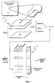
- Fig. 1 is a schematic diagram of four overlapping windows as stored in a frame buffer and visually perceived on the video display.
- Fig. 2 is a schematic diagram of the priority of the windows represented by numerical values related to window planes.
- Fig. 3 is a schematic depiction of the windows in Fig. 1 with a grid overlay of the full content in the frame buffer.
- Fig. 4 is a schematic representation of the frame buffer with the overlay scissored to windows 1, 3 and 4.
- Fig. 5 is a schematic block diagram showing the location and relationship of the mapping memory to the RAMDAC, the associate memory array storing the window, mask and overlay information, and the processor which manipulates the mapping operation.
- Fig. 6 is a schematic diagram representing the functional architecture of the mapping memory.
- Fig. 7 is a schematic diagram portraying the relation of a pixel position on a display screen to overlay data in the mapping memory.
- a graphics processor is used to generate the data stored in the frame buffer.
- the data in the frame buffer is periodically addressed by the display controller using a raster scan technique and then converted from digital to analog format RGB video signals using a conventional RAMDAC.
- the RAMDAC provides one or more color palettes and is responsive to overlay control signals. Window location and priority information, masking plane information, and overlay information are stored in an associate memory array preferably configured in a multiple plane format related by pixel position to the frame buffer.
- a conventional windowed screen image 10 as depicted in Fig. 1.
- the image patterns could represent data stored in the frame buffer or actually generated on a video display screen.
- the image is composed of a background region 1 and for individually numbered windows.
- the priority of the windows is such that windows 2 and 3 overlap and obstruct window 1, such priorities being expressly shown by numerical values in Fig. 2 of the drawings.
- the associate memory array would include for each pixel position of image 10 the binary data representing the hierarchy of the associated window.
- the window information would be stored in 4 bit planes, suitable thereby to differentiate between 16 windows for each pixel position.
- the associate memory contains information differentiating 16 windows, 2 masking planes and 2 overlay planes.
- An overlay such as the grid pattern depicted in Fig. 3, can be placed over the whole of the display pattern or, as shown in Fig. 4, related to specific windows of the display.
- This selected link between the overlay pattern and one or more windows in the display is readily accomplished by relating the overlay patterns to selected window patterns.
- the problem with the prior art arises when one seeks to blink or otherwise manipulate the overlay within the boundaries of one window without doing likewise for the other windows using the same overlay plane. This selectivity is desirable in situations where the blinking or other change of the overlay characteristics are used to relate information such as processing status or cursor position. Since each overlay plane is treated as a unit in a conventional RAMDAC, the blinking action occurs for all locations of the overlay plane.
- the invention provides a means for individually manipulating overlays within the individual windows without requiring a separate overlay plane for each window or mandating a new RAMDAC architecture.
- the invention focuses on the manipulation of data as it appears in the associate memory array to individualize by window the control of window associated overlays. In general, this has been accomplished by recognizing that the bits in the associate memory representing every possible combination of the overlay planes and the protection planes by pixel defines a single and unique address which can be remapped, and thereby subject to individualized manipulation, by altering the mapping transformation.
- the mapping is preferably implemented through the use of a dual address port mapping memory, the memory having one input responsive to a concatenation of the data in the associate memory for a pixel position and the other address port responsive to an address generated by the processor controlling manipulation.
- the output of such mapping memory is an overlay control signal, whose characteristics are a combination of the window, protection and overlay data as selectively modified by the general processor.
- a mapping memory can be defined to uniquely relate an 8 bit address representing the composite window, masking and overlay information for a single pixel to a mapping memory output representing the desired characteristic of the pixel as applied to the overlay input of the RAMDAC.
- the mapping memory of the invention lends itself to selective manipulation in the transformation.
- a conventional general purpose processor can selectively modify window specific data to change by window the overlay input to the RAMDAC.
- the mapping memory data can be cycled to create the aforementioned blinking phenomenon.
- the architecture of the present invention also allows the general purpose processor to change the palette information for an overlay cut or scissored to a specific window.
- Fig. 5 is a schematic block diagram of the basic graphics system to which the invention pertains.
- a graphics processor and display controller 1 communicates with VRAM frame buffer 2 to provide via latch 3 the binary format pixel data to the input of RAMDAC 4.
- the VRAM associate memory 6 is also controlled by graphics processor and display controller 1, storing therein by plane binary data representing window, mask and overlay information.
- frame buffer 2 and associate memory 6 are 1280 x 1024 memory arrays, with the latter configured in eight planes so as to have four planes of window information, two planes of mask information and two planes of overlay information.
- the depth of the frame buffer is at the discretion of the designer, with a typical of 24 to provide 8 bits for each of the colors R, G and B.
- mapping memory 8 is preferably configured as a dual port static RAM, with one address port receiving the output of associate memory 6, synchronized via latch 7, and the other address port receiving selective address signals from general purpose processor 9. Addresses emanating from general purpose processor 9 identify the storage locations for the data provided by processor 9 to mapping memory 8. The output from mapping memory 8 is conveyed to the overlay input of RAMDAC 4.
- the overlay input is not limited merely to on/off manipulation of the pixel data coming from the frame buffer, but can as noted earlier encompass overlay type control of palettes and the like.
- the Texas Instruments TMS 34010 or TMS 34020 has suitable capabilities.
- Toshiba 524-268 is representative of the VRAM devices used in frame buffer 2 and associate memory 6.
- the functions performed in RAMDAC 4 are typical of those available in a BT 461 device manufactured by Brooktree.
- the Cypress CY7C 142 part is representative of the dual port SRAM identified as block 8.
- the general purpose processor function attributed to block 9 can be performed by a Texas Instruments processor identified as TMS 320C30.
- mapping memory 8 is an X x 256 array grouped by addresses in relation to windows 1 to 16.
- An 8 bit address at port 1 produces an X bit data output, which output is the signal to the overlay input connection of RAMDAC 4 (Fig. 5).
- Data is written into mapping memory 8 via the X bit wide DATA IN line and is stored at the address supplied to port 2.
- This arrangement is particularly efficient for implementing overlay control in that the number of bits subject to change is related to the number of windows rather than the number of pixels within a window.
- Fig. 7 portrays by schematic diagram the relation of a pixel 9 on video display screen 11 to the window/mask/overlay planes 12, the data stored in such planes, and the interaction of such data with dual port RAM 8 to provide window selectable overlay information to RAMDAC 4 (Fig. 5).
- dual port RAM 8 is prescribed to be 2 x 256 in size, so as to provide to the RAMDAC overlay input one of four bit combinations ((00,01,10,11).
- the 00 combination will represent a transparent overlay, effectively disabling any overlay.
- the remaining three states of the overlay input are defined by the user and consequently may involve masking or color functions.
- mapping memory note that the data for pixel position 9 as stored in the eight planes 12 is defined by the example to be a string of bits 11110101, wherein the first four bits define one of sixteen windows, the next two bits define the four masks, and the remaining two bits define the overlays.
- This string of bits defines an address within the group of sixteen for window 1111, an address which was previously written by general purpose processor 9 (Fig. 5) to have a 00 bit combination. Consequently, upon mapping the data for pixel position 9 in the eight planes 12 through mapping memory 8 the RAMDAC 4 is provided a 00 bit combination, representing transparency.
- mapping memory 8 is small in relation to the memory planes 12.
- window specific linking can be accomplished by writing small groups of data into mapping memory 8 in timed succession and without modifying significantly larger base of data stored in the planes 12.
- overlay data conveyed to the RAMDAC can be manipulated directly by the general purpose processor in direct relation to a window. Foremost, this flexibility is accomplished within the context of a conventional RAMDAC architecture.
- mapping memory architecture to implement overlays provides indirect benefits as to system flexibility.
- the lookup VRAM by which mapping is accomplished allows masking and overlay planes to be used interchangeably with full masking or overlay capability available individually by window.
- multiple planes can be combined to maximize the available variables, e.g., choices of overlay colors, by eliminating redundant states.
- the invention thus provides for the use of a mapping memory and direct mapping state manipulation by a general processor to temporally and spatially manipulate masking and overlay conditions in relation to system defined window areas while utilizing conventional RAMDAC devices.
- the structures and methods of the present invention also provide versatility and the interchangeability of mask and overlay data as well as expanded capability to individually and selectively manipulate overlays in unmasked windows.
Description
- The present invention relates to display systems and more particularly to apparatus and methods for manipulating binary format data to create specific visual responses on the display. The invention finds particular application in graphics systems, where multiple forms of information are being generated, manipulated and visually portrayed to the user of the system. In such a context it is particularly useful to avoid confusing interaction between the various forms of the information being portrayed.
- Computerized video graphics systems of contemporary design routinely utilize windows to portray independent blocks of information. The user of the system routinely has the power to operate within a window, operate in areas outside a window, or to relate activities of various windows.
- The image portrayed on the video display of the system is normally stored in a memory array conventionally known as a frame buffer. The frame buffer is periodically scanned or otherwise accessed to ascertain the color, intensity and the like information conventionally used to generate the image on the video display itself. The image as stored in the frame buffer is associated with a window mask. Consequently, when a window is removed from view the appropriate underlying image must be regenerated in the changed region of the frame buffer.
- Overlays and masks are two forms of graphics data manipulation which do not change the image as stored in the frame buffer. The advantage of such implementations is that the frame buffer does not have to be modified upon the creation or deletion of such control mechanisms. The effects of masks and overlays for each pixel position are conventionally introduced in the digital-to-analog converter, commonly referred to as a RAMDAC, which is used to convert frame buffer binary data to analog video output signals. The mask plane and overlay plane information supersedes by pixel the related data derived from the frame buffer.
- A representative example of an overlay would be a blinking grid pattern which covers all or part of the video display screen. No manipulation of the image information as stored in the frame buffer is necessary yet the overlay is cyclically introduced by a frame buffer pixel location related override input into the RAMDAC.
- The information representing each overlay plane is normally stored in a memory array analogous to a frame buffer, but with fewer bit planes. Consequently, the graphical effect of the overlay can be related to selected regions of the image in the frame buffer, for example, providing a grid coextensive with two windows within the frame buffer and a pop-up menu for a third window. Unfortunately, in this context, if the overlay is cycled so as to cause a blinking phenomenon on the screen, such as for the objective of drawing attention to one of the windows, the overlay blinks in all of the windows. Consequently, to provide a blinking overlay capability referenced to a window, a complete overlay plane must be consumed for each overlay pattern subject to such independent manipulation. Given the fact that overlays are usually composed of multiple bit planes and provide graphic information over the whole frame buffer image, the size of the memory associated with each overlay is significant and grows in geometric proportion to the pixel count of the screen. It is accordingly an object of this invention to permit to independent association of overlay patterns to multiple windows within the context of a single overlay plane preferably using conventional RAMDAC technology. In such a context, it would be beneficial to have, for example, a single overlay plane provide a first color grid for a first window, a second color checkered pattern for a second window, a blinking overlay in a third window and a pull-down menu in a fourth window, while using a conventional RAMDAC device.
- Accordingly the present invention provides a computer display apparatus for associating overlay patterns with regions in a video display, comprising: a first processing means for storing background and window patterns in a frame buffer memory; storage means for storing overlay characteristics in a first memory; the apparatus being characterised by: the storage means being adapted to store window location information with the overlay characteristics in the first memory; a second processing means for storing in a second memory mapping information for relating the window location and overlay characteristics stored in the first memory to the background and window patterns stored in the frame buffer memory; the second processing means being arranged to selectively modify the mapping information stored in the second memory; and generation means for generating a composite graphics display system signal by synchronously combining window location and overlay characteristics as modified in the second memory with the background and window patterns from the frame buffer memory.
- Further the invention provides a method for associating overlay patterns with regions in a video display, comprising the steps of: employing a first processing means to store background and window patterns in a frame buffer memory; storing overlay characteristics in a first memory; the method being characterised by the steps of: storing window location information with the overlay characteristics in the first memory; employing a second processing means to store in a second memory mapping information for relating the window location and overlay characteristics stored in the first memory to the background and window patterns stored in the frame buffer memory; selectively modifying the mapping information stored in the second memory; and generating a composite graphics display system signal by synchronously combining window location and overlay characteristics as modified in the second memory with the background and window patterns from the frame buffer memory.
- In a preferred embodiment of the invention, window patterns are related to masking and overlay plane patterns through a lookup table configured memory which maps the combination of window, masking, and overlay information to a new overlay. Manipulation, such as blinking of an overlay, is accomplished by changing the content of the relatively small mapping memory in synchronism with the desired changes.
- A preferred architecture for practicing the invention includes a multiple plane associate memory array, distinct from the frame buffer, which stores window, masking, and overlay information, a dual port mapping memory, and a RAMDAC having an overlay input. The output of the associate memory array for each pixel location provides a string of bits with a defined unique address at one port of the mapping memory. The other address port of the mapping memory is under the direct control of a processor to individually define the actions of the overlays by window. The output of the mapping memory drives the overlay control of the RAMDAC. For such a configuration, the controlling processor can independently manipulate the mapping, operation by window address, a manipulation which is thereafter reflected in the overlay signals received and processed by the RAMDAC in generating the video output.
- The architecture and methods of the present invention facilitate operations such as window related blinking of the overlay, the ability to use masking and overlay planes interchangeably, and the ability to use such planes to manipulate palette content by window in the RAMDAC. These and other features of the invention will be more clearly understood and fully appreciated upon considering the ensuing detailed description.
- Background information relating to the technology of the present invention appears in our copending European patent application No 89303077.1 and U.S. Patents 4,317,114; 4,653,020; 4,682,298 and 4,691,295.
- Fig. 1 is a schematic diagram of four overlapping windows as stored in a frame buffer and visually perceived on the video display.
- Fig. 2 is a schematic diagram of the priority of the windows represented by numerical values related to window planes.
- Fig. 3 is a schematic depiction of the windows in Fig. 1 with a grid overlay of the full content in the frame buffer.
- Fig. 4 is a schematic representation of the frame buffer with the overlay scissored to
windows - Fig. 5 is a schematic block diagram showing the location and relationship of the mapping memory to the RAMDAC, the associate memory array storing the window, mask and overlay information, and the processor which manipulates the mapping operation.
- Fig. 6 is a schematic diagram representing the functional architecture of the mapping memory.
- Fig. 7 is a schematic diagram portraying the relation of a pixel position on a display screen to overlay data in the mapping memory.
- The features of the invention will be described in the context of a graphics video display system employing a frame buffer for storing by pixel position digital data representing the color to be generated on the video display. A graphics processor is used to generate the data stored in the frame buffer. The data in the frame buffer is periodically addressed by the display controller using a raster scan technique and then converted from digital to analog format RGB video signals using a conventional RAMDAC. In this context the RAMDAC provides one or more color palettes and is responsive to overlay control signals. Window location and priority information, masking plane information, and overlay information are stored in an associate memory array preferably configured in a multiple plane format related by pixel position to the frame buffer.
- Consider a conventional windowed
screen image 10 as depicted in Fig. 1. The image patterns could represent data stored in the frame buffer or actually generated on a video display screen. The image is composed of abackground region 1 and for individually numbered windows. The priority of the windows is such thatwindows window 1, such priorities being expressly shown by numerical values in Fig. 2 of the drawings. - In the context of this example, the associate memory array would include for each pixel position of
image 10 the binary data representing the hierarchy of the associated window. Preferably, the window information would be stored in 4 bit planes, suitable thereby to differentiate between 16 windows for each pixel position. The invention further contemplates that the associate memory include two additional bit planes, individually allocated to masking functions but by virtue of the present invention fully capable of being used as overlays. And finally, a last two bit planes performing the overlay function. Consequently, the depth of the associate memory would be 4 + 2 + 2 = 8 bits for each pixel position. As thus defined, the associate memory contains information differentiating 16 windows, 2 masking planes and 2 overlay planes. - An overlay, such as the grid pattern depicted in Fig. 3, can be placed over the whole of the display pattern or, as shown in Fig. 4, related to specific windows of the display. This selected link between the overlay pattern and one or more windows in the display is readily accomplished by relating the overlay patterns to selected window patterns. The problem with the prior art arises when one seeks to blink or otherwise manipulate the overlay within the boundaries of one window without doing likewise for the other windows using the same overlay plane. This selectivity is desirable in situations where the blinking or other change of the overlay characteristics are used to relate information such as processing status or cursor position. Since each overlay plane is treated as a unit in a conventional RAMDAC, the blinking action occurs for all locations of the overlay plane. The invention provides a means for individually manipulating overlays within the individual windows without requiring a separate overlay plane for each window or mandating a new RAMDAC architecture.
- The invention focuses on the manipulation of data as it appears in the associate memory array to individualize by window the control of window associated overlays. In general, this has been accomplished by recognizing that the bits in the associate memory representing every possible combination of the overlay planes and the protection planes by pixel defines a single and unique address which can be remapped, and thereby subject to individualized manipulation, by altering the mapping transformation. The mapping is preferably implemented through the use of a dual address port mapping memory, the memory having one input responsive to a concatenation of the data in the associate memory for a pixel position and the other address port responsive to an address generated by the processor controlling manipulation. The output of such mapping memory is an overlay control signal, whose characteristics are a combination of the window, protection and overlay data as selectively modified by the general processor.
- The invention originates from the recognition that there exists a unique mappable relationship between the overlays and the window addresses. Thus, according to the invention, a mapping memory can be defined to uniquely relate an 8 bit address representing the composite window, masking and overlay information for a single pixel to a mapping memory output representing the desired characteristic of the pixel as applied to the overlay input of the RAMDAC. The mapping memory of the invention lends itself to selective manipulation in the transformation. With this architecture a conventional general purpose processor can selectively modify window specific data to change by window the overlay input to the RAMDAC. For example, the mapping memory data can be cycled to create the aforementioned blinking phenomenon. As a variant thereof, where the RAMDAC has a capability to select palettes, the architecture of the present invention also allows the general purpose processor to change the palette information for an overlay cut or scissored to a specific window.
- Fig. 5 is a schematic block diagram of the basic graphics system to which the invention pertains. As depicted therein, a graphics processor and
display controller 1 communicates withVRAM frame buffer 2 to provide vialatch 3 the binary format pixel data to the input ofRAMDAC 4. TheVRAM associate memory 6 is also controlled by graphics processor anddisplay controller 1, storing therein by plane binary data representing window, mask and overlay information. Note thatframe buffer 2 andassociate memory 6 are 1280 x 1024 memory arrays, with the latter configured in eight planes so as to have four planes of window information, two planes of mask information and two planes of overlay information. The depth of the frame buffer is at the discretion of the designer, with a typical of 24 to provide 8 bits for each of the colors R, G and B. The invention differs from the prior art in that the output data fromassociate memory 6 is used as an address tomapping memory 8.Mapping memory 8 is preferably configured as a dual port static RAM, with one address port receiving the output ofassociate memory 6, synchronized vialatch 7, and the other address port receiving selective address signals fromgeneral purpose processor 9. Addresses emanating fromgeneral purpose processor 9 identify the storage locations for the data provided byprocessor 9 tomapping memory 8. The output frommapping memory 8 is conveyed to the overlay input ofRAMDAC 4. The overlay input is not limited merely to on/off manipulation of the pixel data coming from the frame buffer, but can as noted earlier encompass overlay type control of palettes and the like. - Though the function performed in
block 1 would commonly be provided by a custom designed device, the Texas Instruments TMS 34010 or TMS 34020 has suitable capabilities. Toshiba 524-268 is representative of the VRAM devices used inframe buffer 2 andassociate memory 6. The functions performed inRAMDAC 4 are typical of those available in a BT 461 device manufactured by Brooktree. The Cypress CY7C 142 part is representative of the dual port SRAM identified asblock 8. The general purpose processor function attributed to block 9 can be performed by a Texas Instruments processor identified as TMS 320C30. - A particul-arized transformation architecture for
mapping memory 8 is depicted in Fig. 6 of the drawings. Given that the input address is composed of 8 bits of concatenated window, masking, and overlay plane data from associate memory 6 (Fig. 5),mapping memory 8 is an X x 256 array grouped by addresses in relation towindows 1 to 16. An 8 bit address atport 1 produces an X bit data output, which output is the signal to the overlay input connection of RAMDAC 4 (Fig. 5). Data is written intomapping memory 8 via the X bit wide DATA IN line and is stored at the address supplied toport 2. This arrangement is particularly efficient for implementing overlay control in that the number of bits subject to change is related to the number of windows rather than the number of pixels within a window. - Fig. 7 portrays by schematic diagram the relation of a
pixel 9 onvideo display screen 11 to the window/mask/overlay planes 12, the data stored in such planes, and the interaction of such data withdual port RAM 8 to provide window selectable overlay information to RAMDAC 4 (Fig. 5). According to the particularized design depicted in Fig. 7,dual port RAM 8 is prescribed to be 2 x 256 in size, so as to provide to the RAMDAC overlay input one of four bit combinations ((00,01,10,11). Typically the 00 combination will represent a transparent overlay, effectively disabling any overlay. The remaining three states of the overlay input are defined by the user and consequently may involve masking or color functions. In the context of this depicted mapping memory, note that the data forpixel position 9 as stored in the eightplanes 12 is defined by the example to be a string ofbits 11110101, wherein the first four bits define one of sixteen windows, the next two bits define the four masks, and the remaining two bits define the overlays. This string of bits defines an address within the group of sixteen for window 1111, an address which was previously written by general purpose processor 9 (Fig. 5) to have a 00 bit combination. Consequently, upon mapping the data forpixel position 9 in the eightplanes 12 throughmapping memory 8 theRAMDAC 4 is provided a 00 bit combination, representing transparency. Thereby, overlay data, and the mask data of so desired, are mapped through the dual port memory to accomplish window specific manipulation of the information conveyed to the RAMDAC by general purpose processor 9 (Fig. 5). It is particularly noteworthy that the size ofmapping memory 8 is small in relation to the memory planes 12. Thus window specific linking can be accomplished by writing small groups of data intomapping memory 8 in timed succession and without modifying significantly larger base of data stored in theplanes 12. - Note that the overlay data conveyed to the RAMDAC can be manipulated directly by the general purpose processor in direct relation to a window. Foremost, this flexibility is accomplished within the context of a conventional RAMDAC architecture.
- The use of a mapping memory architecture to implement overlays provides indirect benefits as to system flexibility. The lookup VRAM by which mapping is accomplished allows masking and overlay planes to be used interchangeably with full masking or overlay capability available individually by window. Secondly, multiple planes can be combined to maximize the available variables, e.g., choices of overlay colors, by eliminating redundant states.
- The invention thus provides for the use of a mapping memory and direct mapping state manipulation by a general processor to temporally and spatially manipulate masking and overlay conditions in relation to system defined window areas while utilizing conventional RAMDAC devices. The structures and methods of the present invention also provide versatility and the interchangeability of mask and overlay data as well as expanded capability to individually and selectively manipulate overlays in unmasked windows.
- Though the invention has been described and illustrated by way of specific embodiment, the methods and structures should be understood to encompass the full scope of practices defined by the claims set forth hereinafter.
Claims (7)
- A computer display apparatus for associating overlay patterns with regions in a video display, comprising:a first processing means (1) for storing background and window patterns in a frame buffer memory (2);storage means for storing overlay characteristics in a first memory (6);the apparatus being characterised by:the storage means being adapted to store window location information with the overlay characteristics in the first memory (6);a second processing means (9) for storing in a second memory (8) mapping information for relating the window location and overlay characteristics stored in the first memory (6) to the background and window patterns stored in the frame buffer memory (2);the second processing means (9) being arranged to selectively modify the mapping information stored in the second memory (8); andgeneration means (4) for generating a composite graphics display system signal by synchronously combining window location and overlay characteristics as modified in the second memory (8) with the background and window patterns from the frame buffer memory (2).
- An apparatus as claimed in claim 1, wherein the output from the second memory (8) received by the generation means (4) consists of overlay control signals resulting from the mapping of the window location and overlay characteristics within the second memory.
- An apparatus as claimed in claim 1 or claim 2, wherein the window location and overlay characteristics subject to mapping are related to addresses for selecting the background and window patterns stored in the frame buffer memory (2).
- An apparatus as claimed in any of claims 1 to 3, wherein the generation means includes means for combining selectively mapped stored window location and overlay characteristics in synchronism with a scan of the pattern in the frame buffer memory (2).
- An apparatus as claimed in any of claims 2 to 4, wherein the overlay control signals and patterns stored in the frame buffer memory are combined in a RAMDAC.
- A method for associating overlay patterns with regions in a video display, comprising the steps of:employing a first processing means (1) to store background and window patterns in a frame buffer memory (2);storing overlay characteristics in a first memory (6);the method being characterised by the steps of:storing window location information with the overlay characteristics in the first memory (6);employing a second processing means (9) to store in a second memory (8) mapping information for relating the window location and overlay characteristics stored in the first memory (6) to the background and window patterns stored in the frame buffer memory (2);selectively modifying the mapping information stored in the second memory; andgenerating a composite graphics display system signal by synchronously combining window location and overlay characteristics as modified in the second memory (8) with the background and window patterns from the frame buffer memory (2).
- A method as claimed in claim 6, wherein said step of generating is accomplished by synchronously scanning the memories for combination in a RAMDAC.
Applications Claiming Priority (2)
| Application Number | Priority Date | Filing Date | Title |
|---|---|---|---|
| US52150390A | 1990-05-10 | 1990-05-10 | |
| US521503 | 1990-05-10 |
Publications (3)
| Publication Number | Publication Date |
|---|---|
| EP0456411A2 EP0456411A2 (en) | 1991-11-13 |
| EP0456411A3 EP0456411A3 (en) | 1992-10-07 |
| EP0456411B1 true EP0456411B1 (en) | 1996-03-13 |
Family
ID=24077000
Family Applications (1)
| Application Number | Title | Priority Date | Filing Date |
|---|---|---|---|
| EP91303969A Expired - Lifetime EP0456411B1 (en) | 1990-05-10 | 1991-05-01 | Graphics display system |
Country Status (4)
| Country | Link |
|---|---|
| US (1) | US5469541A (en) |
| EP (1) | EP0456411B1 (en) |
| JP (1) | JPH04226495A (en) |
| DE (1) | DE69117798T2 (en) |
Families Citing this family (22)
| Publication number | Priority date | Publication date | Assignee | Title |
|---|---|---|---|---|
| JPH0685144B2 (en) * | 1990-11-15 | 1994-10-26 | インターナショナル・ビジネス・マシーンズ・コーポレイション | Selective controller for overlay and underlay |
| US5712994A (en) * | 1992-08-10 | 1998-01-27 | International Business Machines Corporation | Method and system for apparent direct editing of transient graphic elements within a data processing system |
| JP2583003B2 (en) * | 1992-09-11 | 1997-02-19 | インターナショナル・ビジネス・マシーンズ・コーポレイション | Image display method, frame buffer, and graphics display system in graphics display system |
| US5638501A (en) | 1993-05-10 | 1997-06-10 | Apple Computer, Inc. | Method and apparatus for displaying an overlay image |
| US5754186A (en) * | 1993-05-10 | 1998-05-19 | Apple Computer, Inc. | Method and apparatus for blending images |
| US5815143A (en) * | 1993-10-13 | 1998-09-29 | Hitachi Computer Products (America) | Video picture display device and method for controlling video picture display |
| JP3462566B2 (en) * | 1994-04-08 | 2003-11-05 | 株式会社ソニー・コンピュータエンタテインメント | Image generation device |
| EP0734010B1 (en) * | 1995-03-21 | 2005-01-26 | Sun Microsystems, Inc. | Video frame signature capture |
| US5977960A (en) * | 1996-09-10 | 1999-11-02 | S3 Incorporated | Apparatus, systems and methods for controlling data overlay in multimedia data processing and display systems using mask techniques |
| GB2352601A (en) * | 1999-07-26 | 2001-01-31 | Pixelfusion Ltd | Graphical data-processing |
| US9189467B1 (en) | 2001-11-07 | 2015-11-17 | Apple Inc. | Method and apparatus for annotating an electronic document |
| US20040216036A1 (en) * | 2002-09-13 | 2004-10-28 | Yahoo! Inc. | Browser user interface |
| EP1679604A4 (en) * | 2003-10-29 | 2009-08-12 | Panasonic Corp | Electronic document reading system |
| US20060026530A1 (en) * | 2004-07-30 | 2006-02-02 | Texas Instruments Incorporated | DMA overlay addressing methodology for optimizing power and improving memory bandwidth for display engines |
| JP4915850B2 (en) * | 2006-09-15 | 2012-04-11 | 株式会社リコー | Image processing apparatus and image display apparatus |
| US11076189B2 (en) * | 2009-03-30 | 2021-07-27 | Time Warner Cable Enterprises Llc | Personal media channel apparatus and methods |
| US8986204B2 (en) * | 2009-11-16 | 2015-03-24 | John Allen Pacey | Telemedicine systems and methods |
| US9092128B2 (en) | 2010-05-21 | 2015-07-28 | Apple Inc. | Method and apparatus for managing visual information |
| US8645609B2 (en) * | 2010-12-06 | 2014-02-04 | Brocade Communications Systems, Inc. | Two-port memory implemented with single-port memory blocks |
| WO2014125319A1 (en) | 2013-02-12 | 2014-08-21 | Freescale Semiconductor, Inc. | Display processor and method for display processing |
| US10116676B2 (en) | 2015-02-13 | 2018-10-30 | Time Warner Cable Enterprises Llc | Apparatus and methods for data collection, analysis and service modification based on online activity |
| CN106708452B (en) * | 2015-11-17 | 2019-12-13 | 腾讯科技(深圳)有限公司 | Information sharing method and terminal |
Family Cites Families (14)
| Publication number | Priority date | Publication date | Assignee | Title |
|---|---|---|---|---|
| US4149184A (en) * | 1977-12-02 | 1979-04-10 | International Business Machines Corporation | Multi-color video display systems using more than one signal source |
| US4317114A (en) * | 1980-05-12 | 1982-02-23 | Cromemco Inc. | Composite display device for combining image data and method |
| US4555775B1 (en) * | 1982-10-07 | 1995-12-05 | Bell Telephone Labor Inc | Dynamic generation and overlaying of graphic windows for multiple active program storage areas |
| US4691295A (en) * | 1983-02-28 | 1987-09-01 | Data General Corporation | System for storing and retreiving display information in a plurality of memory planes |
| JPS59205667A (en) * | 1983-05-09 | 1984-11-21 | Sharp Corp | Pattern blinking system of graphic display device |
| US4653020A (en) * | 1983-10-17 | 1987-03-24 | International Business Machines Corporation | Display of multiple data windows in a multi-tasking system |
| JPS60176093A (en) * | 1984-02-23 | 1985-09-10 | 富士ゼロックス株式会社 | Image display unit |
| JPS60220387A (en) * | 1984-04-13 | 1985-11-05 | インタ−ナショナル ビジネス マシ−ンズ コ−ポレ−ション | Raster scan display unit |
| US4663619A (en) * | 1985-04-08 | 1987-05-05 | Honeywell Inc. | Memory access modes for a video display generator |
| US4812834A (en) * | 1985-08-01 | 1989-03-14 | Cadtrak Corporation | Graphics display system with arbitrary overlapping viewports |
| JPS63670A (en) * | 1986-06-05 | 1988-01-05 | Hitachi Ltd | Multi-window control method |
| US4845640A (en) * | 1987-03-11 | 1989-07-04 | Megascan Technology, Inc. | High-speed dual mode graphics memory |
| US4970664A (en) * | 1988-06-10 | 1990-11-13 | Kaiser Richard R | Critical path analyzer with path context window |
| US5263134A (en) * | 1989-10-25 | 1993-11-16 | Apple Computer, Inc. | Method and apparatus for controlling computer displays by using a two dimensional scroll palette |
-
1991
- 1991-04-09 JP JP3103800A patent/JPH04226495A/en active Pending
- 1991-05-01 EP EP91303969A patent/EP0456411B1/en not_active Expired - Lifetime
- 1991-05-01 DE DE69117798T patent/DE69117798T2/en not_active Expired - Fee Related
-
1994
- 1994-10-25 US US08/328,591 patent/US5469541A/en not_active Expired - Fee Related
Also Published As
| Publication number | Publication date |
|---|---|
| JPH04226495A (en) | 1992-08-17 |
| US5469541A (en) | 1995-11-21 |
| EP0456411A3 (en) | 1992-10-07 |
| DE69117798T2 (en) | 1996-09-26 |
| DE69117798D1 (en) | 1996-04-18 |
| EP0456411A2 (en) | 1991-11-13 |
Similar Documents
| Publication | Publication Date | Title |
|---|---|---|
| EP0456411B1 (en) | Graphics display system | |
| US5386505A (en) | Selective control of window related overlays and underlays | |
| US5475812A (en) | Method and system for independent control of multiple windows in a graphics display system | |
| US4933878A (en) | Graphics data processing apparatus having non-linear saturating operations on multibit color data | |
| US4931956A (en) | Video image creation systems | |
| US4818979A (en) | LUT output for graphics display | |
| JPS59501179A (en) | Video image overlay system with interactive color addresses | |
| US5128658A (en) | Pixel data formatting | |
| US5815137A (en) | High speed display system having cursor multiplexing scheme | |
| JPH0426471B2 (en) | ||
| US4935730A (en) | Display apparatus | |
| US5440680A (en) | Image display controller having a common memory for storage of image overlay data and window identification data | |
| EP0798689B1 (en) | Display processor system for bit-mapped displays of waveform data | |
| US4692759A (en) | Apparatus for modifying the appearance of the points of an image on the screen of a graphic image display console | |
| JPH0325493A (en) | Color display | |
| JP2508544B2 (en) | Graphic display device | |
| JPS601647B2 (en) | information input device | |
| JPS62198908A (en) | Drawing method for numerical controller | |
| JP2703219B2 (en) | Image processing device | |
| JPH01248189A (en) | Cursor display control circuit | |
| JPS5972517A (en) | Numerical controller containing graphic display device | |
| JPH04305161A (en) | Waveform observing apparatus | |
| JPH05323280A (en) | Display control system | |
| JPS628790B2 (en) | ||
| JPH07140948A (en) | Display device |
Legal Events
| Date | Code | Title | Description |
|---|---|---|---|
| PUAI | Public reference made under article 153(3) epc to a published international application that has entered the european phase |
Free format text: ORIGINAL CODE: 0009012 |
|
| AK | Designated contracting states |
Kind code of ref document: A2 Designated state(s): DE FR GB |
|
| 17P | Request for examination filed |
Effective date: 19911219 |
|
| PUAL | Search report despatched |
Free format text: ORIGINAL CODE: 0009013 |
|
| AK | Designated contracting states |
Kind code of ref document: A3 Designated state(s): DE FR GB |
|
| 17Q | First examination report despatched |
Effective date: 19940704 |
|
| GRAA | (expected) grant |
Free format text: ORIGINAL CODE: 0009210 |
|
| AK | Designated contracting states |
Kind code of ref document: B1 Designated state(s): DE FR GB |
|
| REF | Corresponds to: |
Ref document number: 69117798 Country of ref document: DE Date of ref document: 19960418 |
|
| PGFP | Annual fee paid to national office [announced via postgrant information from national office to epo] |
Ref country code: FR Payment date: 19960507 Year of fee payment: 6 |
|
| ET | Fr: translation filed | ||
| PLBE | No opposition filed within time limit |
Free format text: ORIGINAL CODE: 0009261 |
|
| STAA | Information on the status of an ep patent application or granted ep patent |
Free format text: STATUS: NO OPPOSITION FILED WITHIN TIME LIMIT |
|
| 26N | No opposition filed | ||
| PG25 | Lapsed in a contracting state [announced via postgrant information from national office to epo] |
Ref country code: FR Free format text: LAPSE BECAUSE OF NON-PAYMENT OF DUE FEES Effective date: 19980130 |
|
| REG | Reference to a national code |
Ref country code: FR Ref legal event code: ST |
|
| PGFP | Annual fee paid to national office [announced via postgrant information from national office to epo] |
Ref country code: GB Payment date: 19990428 Year of fee payment: 9 |
|
| PG25 | Lapsed in a contracting state [announced via postgrant information from national office to epo] |
Ref country code: GB Free format text: LAPSE BECAUSE OF NON-PAYMENT OF DUE FEES Effective date: 20000501 |
|
| GBPC | Gb: european patent ceased through non-payment of renewal fee |
Effective date: 20000501 |
|
| PGFP | Annual fee paid to national office [announced via postgrant information from national office to epo] |
Ref country code: DE Payment date: 20010914 Year of fee payment: 11 |
|
| PG25 | Lapsed in a contracting state [announced via postgrant information from national office to epo] |
Ref country code: DE Free format text: LAPSE BECAUSE OF NON-PAYMENT OF DUE FEES Effective date: 20021203 |