EP0451595B1 - Short circuit detector circuit for memory array - Google Patents
Short circuit detector circuit for memory array Download PDFInfo
- Publication number
- EP0451595B1 EP0451595B1 EP91104705A EP91104705A EP0451595B1 EP 0451595 B1 EP0451595 B1 EP 0451595B1 EP 91104705 A EP91104705 A EP 91104705A EP 91104705 A EP91104705 A EP 91104705A EP 0451595 B1 EP0451595 B1 EP 0451595B1
- Authority
- EP
- European Patent Office
- Prior art keywords
- circuit
- coupled
- current
- row
- transistor
- Prior art date
- Legal status (The legal status is an assumption and is not a legal conclusion. Google has not performed a legal analysis and makes no representation as to the accuracy of the status listed.)
- Expired - Lifetime
Links
Images

Classifications
-
- G—PHYSICS
- G11—INFORMATION STORAGE
- G11C—STATIC STORES
- G11C11/00—Digital stores characterised by the use of particular electric or magnetic storage elements; Storage elements therefor
- G11C11/21—Digital stores characterised by the use of particular electric or magnetic storage elements; Storage elements therefor using electric elements
- G11C11/34—Digital stores characterised by the use of particular electric or magnetic storage elements; Storage elements therefor using electric elements using semiconductor devices
- G11C11/40—Digital stores characterised by the use of particular electric or magnetic storage elements; Storage elements therefor using electric elements using semiconductor devices using transistors
- G11C11/41—Digital stores characterised by the use of particular electric or magnetic storage elements; Storage elements therefor using electric elements using semiconductor devices using transistors forming static cells with positive feedback, i.e. cells not needing refreshing or charge regeneration, e.g. bistable multivibrator or Schmitt trigger
- G11C11/413—Auxiliary circuits, e.g. for addressing, decoding, driving, writing, sensing, timing or power reduction
- G11C11/417—Auxiliary circuits, e.g. for addressing, decoding, driving, writing, sensing, timing or power reduction for memory cells of the field-effect type
-
- G—PHYSICS
- G11—INFORMATION STORAGE
- G11C—STATIC STORES
- G11C29/00—Checking stores for correct operation ; Subsequent repair; Testing stores during standby or offline operation
- G11C29/04—Detection or location of defective memory elements, e.g. cell constructio details, timing of test signals
- G11C29/50—Marginal testing, e.g. race, voltage or current testing
Definitions
- This invention relates to Static Random Access Memories ("SRAMs").
- SRAMs Static Random Access Memories
- a circuit which can be incorporated into a SRAM to simplify the detection of power supply short circuits within arrays of SRAM memory cells.
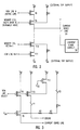
- FIG. 1a A generic SRAM memory cell is shown in Figure 1a. The construction and operation of such cells is known.
- transistor T1 is the driver and transistor T3 the load for an inverter that is cross-coupled to a second inverter formed from transistors T2 and T4, the two inverters forming a storage flip-flop.
- output Q is a logic 1 (herein, +5V).
- transistors T5 and T6 With the row-select line low (0V), transistors T5 and T6 are off, and the cell is isolated from both bit lines.
- transistors T5 and T6 couple the bit lines to the cell and output Q appears on bit line D.
- a sense amplifier is connected to the bit line to provide output buffering, and the proper logic level appears on the sense output line.
- the selected row of cells is connected to the bit lines, and Q or Q is set or reset by a logic 1 (+5V) placed on bit line D or D by the write amplifiers while a logic 0 (0V) is placed on the complement bit line.
- the state of the flip-flop persists as long as power is supplied to the chip, and it is not altered by the read operation. It should be understood that an SRAM chip will comprise many thousands of such memory cells.
- transistors T1and T2 have a certain amount of capacitance, shown in Figure 1a as capacitors C1 and C2. If V dd were shorted to V ss , due to a manufacturing error, a certain amount of time would be required before the charge present on either C1 and C2 (the nature of the flip-flop requires that either Q or Q be high (+5V), but not both) is drained through transistors T3 and T4 to V ss . This discharge time is often large in comparison to the amount of time required to access the memory cell and the frequency of such access. It is therefore quite possible to read data several times from a cell with such a short circuit before the charge is dissipated sufficiently to detect the presence of the short.
- EP-A-0 146 975 discloses a short detection circuit incorporated in a programmable read only memory so that a selected positive voltage can be applied across each memory cell to allow the detection, prior to programming, of shorts between bit lines and word lines and shorts or leaks in a memory cell. By measuring the current flowing into the bit lines shorts or leaky junctions within memory cells can be detected in unprogrammed devices prior to actual delivery to a customer.
- the short detection circuit is isolated from the memory during normal operation thereof so that it does not have an adverse effect on the operation of the PROM.
- each row of memory cells is individually activated and scanned.
- Each row select line is coupled to a common current sense line, which in turn is coupled to a current sense circuit.
- each successive row of memory cells is activated. If the voltage supply (V dd ) for that row of cells is shorted to ground (V ss ) or any lower voltage for any reason a current will flow through the current sense line and will be detected by the current sense circuit.
- the circuit which selects individual rows of memory cells for testing also provides a means for uniquely identifying the memory chip. Certain fuses within the select circuit can be selectively blown, the pattern of open fuses providing the identification information.
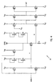
- FIG 1a shows how each prior art SRAM memory cell is individually coupled to a row select line and to V dd , herein, by example only, +5V.
- the SRAM cell receives V dd ′, V dd being first coupled to R1 which resistor limits the amount of current which can flow through the voltage supply lines to the memory cell.
- Each cell is coupled to a row line, shown in Figure 2 as row lines N and N + 1.
- the cells are not illustrated in Figure 2.
- each cell is coupled to the current sense row selector circuit shown in Figure 2 by means of the memory cell's row select line and its V dd ′ voltage supply line.
- the memory cell's row select line and its V dd ′ voltage supply line There can be any arbitrary number of rows of memory cells.
- Row line N and memory cell supply V dd ′N are coupled respectively to the gates of PMOS transistors T8 and T9. Similarly, the gates of transistors T10 and T11 are coupled respectively to memory cell supply V dd ′N+1 and row line N + 1.
- V dd ′ voltage supply V dd ′ to the cell can be inadvertently shorted to either V ss or, possibly, to a row line which is active low (0V) as a result of a manufacturing defect.
- Such short circuits can be detected by using this invention in a test mode.
- each consecutive row of memory cells is scanned.
- PMOS transistor T8 turns on.
- V dd ′ is shorted low for any reason, transistor T9 will also turn on. Current will then flow through current sense line 20 ( Figure 2) to current sense circuit 30.
- the current sense circuit detects even small current flows through the current sense line when the SRAM is being tested. It outputs a logic signal to indicate if such a flow is detected.
- transistors T8 and T9 whose gates are respectively coupled to the row select signal and V dd ′, the isolated memory matrix supply voltage, act to detect shorts in the matrix between V dd ′ and either V ss or the row select signal, which is active low. This is done by selecting a particular row, whereby that row's select signal goes low and transistor T8 turns on. If V dd ′ is low, the result of a short circuit, transistor T9 will turn on and current will flow along the SSTENS line (current sense line 20, Figure 2) to current sensing circuit 30 ( Figure 2) during the supply short circuits test mode.
- Transistor T12 is a pull-up transistor for the row select signal which maintains a high voltage level of V dd for nonselected row select lines.
- the row select circuit provides a circuit ID encoding scheme. This is done in a similar fashion to the voltage supply short circuit test.
- the row select signal selects the appropriate row. If fuse F1 is not open, current will flow through the IDSENS signal line. There is one fuse per row of memory cells and it can be blown or not blown to encode the chip lot and wafer number or other desired information.
- Resistors R2, R3 and R4 are used to isolate the memory cell top supply V dd ′ from the external supply V dd . Doing so limits the current that can flow if a short circuit occurs to approximately 1 ma. If fuse F2 opens, the flow of current stops completely.
- FIG. 4 A detailed schematic drawing of current sensing circuit 30 is shown in Figure 4.
- the MODE signal is used to turn the sensing circuit on during test mode.
- node A is set at V dd - 2V be (transistor T22 and T24 providing the requisite 2V be drops) as a reference voltage level for the gate of PMOS transistor T26.
- T26 serves as a cascode device coupled to the bottom rail of circuit 30.
- Transistor T23 When not in the matrix voltage supply short circuit test mode, the MODE signal is low.
- Transistor T23 is off and transistor T21 is on, holding node A at the supply voltage V dd .
- transistor T26 turns off, allowing resistor R1 to hold node B low.
- Transistor pairs T29/T31, T32/T34 and T35/T37 act as inverters so when node B is low, the output ('OUT') of the circuit is high.
- the MODE signal is high. This turns off transistors T21 and T25 and turns transistor T23 on. With transistor T23 on, node A is biased to V dd - 2V be , the voltage drop through T22 and T24. Node B will change voltage as current modulation occurs along the SENSLINE signal in test mode. When current is sensed, node B will rise, tripping the three inverters that drive the OUT output signal. The beta ratio for the first inverter (T29/T31) is low to allow node B, which has a small voltage swing, to trip the three inverters. Bipolar transistors T27 and T28 are used to clamp the low level voltage to a certain minimum on the SENSLINE signal line to prevent SENSLINE voltage from coupling around. Transistor T26 will clamp the high level of the SENSLINE signal to V dd - 2V be + V tp .
Abstract
Description
- This invention relates to Static Random Access Memories ("SRAMs"). In particular, it relates to a circuit which can be incorporated into a SRAM to simplify the detection of power supply short circuits within arrays of SRAM memory cells.
- A generic SRAM memory cell is shown in Figure 1a. The construction and operation of such cells is known. In the illustrated cell, transistor T₁ is the driver and transistor T₃ the load for an inverter that is cross-coupled to a second inverter formed from transistors T₂ and T₄, the two inverters forming a storage flip-flop. When transistor T₂ is on and transistor T₁ is off, output Q is a logic 1 (herein, +5V). With the row-select line low (0V), transistors T₅ and T₆ are off, and the cell is isolated from both bit lines. When the memory cell is read, as soon as the row-select line goes high (+5V), transistors T₅ and T₆ couple the bit lines to the cell and output Q appears on bit line D.
- As shown in Figure 1b, a sense amplifier is connected to the bit line to provide output buffering, and the proper logic level appears on the sense output line. In a write operation, the selected row of cells is connected to the bit lines, and Q or
Q is set or reset by a logic 1 (+5V) placed on bit line D orD by the write amplifiers while a logic 0 (0V) is placed on the complement bit line. In this SRAM with nondestructive readout, the state of the flip-flop persists as long as power is supplied to the chip, and it is not altered by the read operation. It should be understood that an SRAM chip will comprise many thousands of such memory cells. - In normal operations, transistors T₁and T₂ have a certain amount of capacitance, shown in Figure 1a as capacitors C₁ and C₂. If Vdd were shorted to Vss, due to a manufacturing error, a certain amount of time would be required before the charge present on either C₁ and C₂ (the nature of the flip-flop requires that either Q or
Q be high (+5V), but not both) is drained through transistors T₃ and T₄ to Vss. This discharge time is often large in comparison to the amount of time required to access the memory cell and the frequency of such access. It is therefore quite possible to read data several times from a cell with such a short circuit before the charge is dissipated sufficiently to detect the presence of the short. - This long dissipation time makes testing for this type of short circuit a long, tedious and costly process. A method and/or an apparatus which can speed the process of testing for and detecting such power supply short circuits is needed.
- The document EP-A-0 146 975 discloses a short detection circuit incorporated in a programmable read only memory so that a selected positive voltage can be applied across each memory cell to allow the detection, prior to programming, of shorts between bit lines and word lines and shorts or leaks in a memory cell. By measuring the current flowing into the bit lines shorts or leaky junctions within memory cells can be detected in unprogrammed devices prior to actual delivery to a customer. The short detection circuit is isolated from the memory during normal operation thereof so that it does not have an adverse effect on the operation of the PROM.
- The present invention as defined in the independent claims provides a method to test an array of SRAM memory cells for power supply short circuits. It also provides a circuit for detecting such short circuits in conjunction with the testing method. According to one embodiment, each row of memory cells is individually activated and scanned. Each row select line is coupled to a common current sense line, which in turn is coupled to a current sense circuit. In operation, each successive row of memory cells is activated. If the voltage supply (Vdd) for that row of cells is shorted to ground (Vss) or any lower voltage for any reason a current will flow through the current sense line and will be detected by the current sense circuit.
- The circuit which selects individual rows of memory cells for testing also provides a means for uniquely identifying the memory chip. Certain fuses within the select circuit can be selectively blown, the pattern of open fuses providing the identification information.
- The present invention will now be described in detail with reference to the following figures.
- Figure 1a shows a typical SRAM memory cell;
- Figure 1b shows the write and sense amplifiers coupled to the SRAM memory cell;
- Figure 2 shows the current sense row selector circuit;
- Figure 3 is a detailed schematic of the row selector circuit; and
- Figure 4 is a detailed schematic of the current sensing circuit.
- Figure 1a shows how each prior art SRAM memory cell is individually coupled to a row select line and to Vdd, herein, by example only, +5V. In the present invention, as shown in Figure 2, the SRAM cell receives Vdd′, Vdd being first coupled to R₁ which resistor limits the amount of current which can flow through the voltage supply lines to the memory cell. Each cell is coupled to a row line, shown in Figure 2 as row lines N and N + 1. As the particular workings of the memory cells is not relevant to an understanding of the present invention, the cells are not illustrated in Figure 2. For the purposes of this description, it suffices to state that each cell is coupled to the current sense row selector circuit shown in Figure 2 by means of the memory cell's row select line and its Vdd′ voltage supply line. There can be any arbitrary number of rows of memory cells.
- Row line N and memory cell supply Vdd′N are coupled respectively to the gates of PMOS transistors T₈ and T₉. Similarly, the gates of transistors T₁₀ and T₁₁ are coupled respectively to memory cell supply Vdd′N+1 and row line N + 1.
- In this type of SRAM array, voltage supply Vdd′ to the cell can be inadvertently shorted to either Vss or, possibly, to a row line which is active low (0V) as a result of a manufacturing defect. Such short circuits can be detected by using this invention in a test mode. When the present invention is used in its test mode, each consecutive row of memory cells is scanned. When a row becomes active (row N, for example), PMOS transistor T₈ turns on. If Vdd′ is shorted low for any reason, transistor T₉ will also turn on. Current will then flow through current sense line 20 (Figure 2) to
current sense circuit 30. The current sense circuit, as will be explained, detects even small current flows through the current sense line when the SRAM is being tested. It outputs a logic signal to indicate if such a flow is detected. - A detailed schematic of the row select circuit is shown in Figure 3. As discussed transistors T₈ and T₉, whose gates are respectively coupled to the row select signal and Vdd′, the isolated memory matrix supply voltage, act to detect shorts in the matrix between Vdd′ and either Vss or the row select signal, which is active low. This is done by selecting a particular row, whereby that row's select signal goes low and transistor T₈ turns on. If Vdd′ is low, the result of a short circuit, transistor T₉ will turn on and current will flow along the SSTENS line (
current sense line 20, Figure 2) to current sensing circuit 30 (Figure 2) during the supply short circuits test mode. Transistor T₁₂ is a pull-up transistor for the row select signal which maintains a high voltage level of Vdd for nonselected row select lines. - Another feature of the row select circuit is that it provides a circuit ID encoding scheme. This is done in a similar fashion to the voltage supply short circuit test. The row select signal selects the appropriate row. If fuse F₁ is not open, current will flow through the IDSENS signal line. There is one fuse per row of memory cells and it can be blown or not blown to encode the chip lot and wafer number or other desired information. Resistors R₂, R₃ and R₄ are used to isolate the memory cell top supply Vdd′ from the external supply Vdd. Doing so limits the current that can flow if a short circuit occurs to approximately 1 ma. If fuse F₂ opens, the flow of current stops completely.
- A detailed schematic drawing of
current sensing circuit 30 is shown in Figure 4. The MODE signal is used to turn the sensing circuit on during test mode. In the test mode, node A is set at Vdd - 2Vbe (transistor T₂₂ and T₂₄ providing the requisite 2Vbe drops) as a reference voltage level for the gate of PMOS transistor T₂₆. T₂₆ serves as a cascode device coupled to the bottom rail ofcircuit 30. - When not in the matrix voltage supply short circuit test mode, the MODE signal is low. Transistor T₂₃ is off and transistor T₂₁ is on, holding node A at the supply voltage Vdd. In turn, transistor T₂₆ turns off, allowing resistor R₁ to hold node B low. Transistor pairs T₂₉/T₃₁, T₃₂/T₃₄ and T₃₅/T₃₇ act as inverters so when node B is low, the output ('OUT') of the circuit is high.
- In the test mode, the MODE signal is high. This turns off transistors T₂₁ and T₂₅ and turns transistor T₂₃ on. With transistor T₂₃ on, node A is biased to Vdd - 2Vbe, the voltage drop through T₂₂ and T₂₄. Node B will change voltage as current modulation occurs along the SENSLINE signal in test mode. When current is sensed, node B will rise, tripping the three inverters that drive the OUT output signal. The beta ratio for the first inverter (T₂₉/T₃₁) is low to allow node B, which has a small voltage swing, to trip the three inverters. Bipolar transistors T₂₇ and T₂₈ are used to clamp the low level voltage to a certain minimum on the SENSLINE signal line to prevent SENSLINE voltage from coupling around. Transistor T₂₆ will clamp the high level of the SENSLINE signal to Vdd - 2Vbe + Vtp.
- Although the present invention has been described in the specific environment of a BiCMOS SRAM, its utility is not limited thereto. Its use in any type of SRAM or even in a dynamic random access memory is easily envisioned. Therefore, this application should not be read in a limited sense.
Claims (8)
- A method for testing an array of memory cells for short circuits, the cells being arranged in rows, the method comprising:
coupling the cells of the array to a plurality of row select lines and a current sense line (20), each row of memory cells being coupled to a different row select line;
coupling said current sense line to a current detector circuit (30);
characterized by the steps of:
sequentially activating each row select line; and
detecting whether any current flows through the current sense line when the row select line is activated. - The method of claim 1 wherein the coupling of each row select line to the current detector circuit occurs upon command of a computer coupled to the array of memory cells.
- The method of claim 1 wherein the step of activating each row select line sequentially occurs upon commands received from a computer to which the array of memory cells is coupled.
- A circuit for detecting voltage supply short circuits in an array of static random access memory cells, the cells being arranged in rows and each row being coupled to a row select line, the cells having a power supply, the circuit characterized by:
a first (T8) and second (T9) PMOS transistor coupled in series, their gates being coupled respectively to the voltage supply (V′DD) for the cells and the row select line, the source of the first transistor coupled to the power supply, the drain of the first transistor and the source of the second transistor being coupled together;
a current sense line (20) coupled to the drain from the second PMOS transistor; and
a current detector circuit (30) coupled to the current sense line which provides a logic output signal when current flows in the current sense line. - The circuit of claim 4 wherein said second transistor has its gate coupled to an external power supply (VDD).
- The circuit of claim 5 wherein there is one pair of first and second transistors for each row of memory cells.
- The circuit of claim 4 wherein the current sensing circuit comprises:
first switching network (T21, T23) coupled to a first circuit node (A), the first switching network being coupled to receive a testing mode input signal, the first switching network biasing the first circuit node to the power supply voltage when the testing mode input signal is low and biasing the first circuit node to a lower voltage when the testing mode signal is high:
current sensing transistor means (T25, T26) coupled to the current sense line, the first circuit node and a second circuit node (B), the current sensing transistor means conducting current from the current sense line when the testing mode input signal is high, the voltage at the second circuit node increasing as increasing current flows through the current sensing transistor means; and
inverter output circuit (T29-T37), for outputting a high voltage signal when the voltage at the second circuit node rises above a predefined value, coupled to the second circuit node. - The circuit of claim 7 wherein the inverter output circuit further comprises three inverter logic gates coupled together in series so that a low input value becomes a high output value.
Applications Claiming Priority (2)
| Application Number | Priority Date | Filing Date | Title |
|---|---|---|---|
| US07/507,692 US5181205A (en) | 1990-04-10 | 1990-04-10 | Short circuit detector circuit for memory arrays |
| US507692 | 1995-07-25 |
Publications (3)
| Publication Number | Publication Date |
|---|---|
| EP0451595A2 EP0451595A2 (en) | 1991-10-16 |
| EP0451595A3 EP0451595A3 (en) | 1993-03-10 |
| EP0451595B1 true EP0451595B1 (en) | 1995-12-27 |
Family
ID=24019736
Family Applications (1)
| Application Number | Title | Priority Date | Filing Date |
|---|---|---|---|
| EP91104705A Expired - Lifetime EP0451595B1 (en) | 1990-04-10 | 1991-03-26 | Short circuit detector circuit for memory array |
Country Status (4)
| Country | Link |
|---|---|
| US (1) | US5181205A (en) |
| EP (1) | EP0451595B1 (en) |
| JP (1) | JP3258676B2 (en) |
| DE (1) | DE69115741T2 (en) |
Families Citing this family (25)
| Publication number | Priority date | Publication date | Assignee | Title |
|---|---|---|---|---|
| IL96808A (en) * | 1990-04-18 | 1996-03-31 | Rambus Inc | Integrated circuit i/o using a high performance bus interface |
| JP2978329B2 (en) * | 1992-04-21 | 1999-11-15 | 三菱電機株式会社 | Semiconductor memory device and method for repairing short circuit of bit line thereof |
| US5428621A (en) * | 1992-09-21 | 1995-06-27 | Sundisk Corporation | Latent defect handling in EEPROM devices |
| US5497475A (en) * | 1993-02-05 | 1996-03-05 | National Semiconductor Corporation | Configurable integrated circuit having true and shadow EPROM registers |
| DE69326329T2 (en) * | 1993-06-28 | 2000-04-13 | St Microelectronics Srl | Memory cell current reading method in microcontroller |
| TW243531B (en) * | 1993-09-03 | 1995-03-21 | Motorola Inc | |
| WO1996013003A1 (en) * | 1994-10-19 | 1996-05-02 | Micron Technology, Inc. | An efficient method for obtaining usable parts from a partially good memory integrated circuit |
| DE19612441C2 (en) * | 1996-03-28 | 1998-04-09 | Siemens Ag | Circuit arrangement with a test circuit |
| US5889410A (en) * | 1996-05-22 | 1999-03-30 | International Business Machines Corporation | Floating gate interlevel defect monitor and method |
| US5946257A (en) * | 1996-07-24 | 1999-08-31 | Micron Technology, Inc. | Selective power distribution circuit for an integrated circuit |
| JP3544073B2 (en) * | 1996-09-03 | 2004-07-21 | 株式会社 沖マイクロデザイン | Semiconductor memory device test method and semiconductor memory device |
| US5748554A (en) * | 1996-12-20 | 1998-05-05 | Rambus, Inc. | Memory and method for sensing sub-groups of memory elements |
| ES2203780T3 (en) * | 1997-03-04 | 2004-04-16 | Stmicroelectronics S.R.L. | A DETECTION DEVICE FOR SHORT CIRCUITS. |
| US5815452A (en) * | 1997-06-12 | 1998-09-29 | Enable Semiconductor, Inc. | High-speed asynchronous memory with current-sensing sense amplifiers |
| US7500075B1 (en) | 2001-04-17 | 2009-03-03 | Rambus Inc. | Mechanism for enabling full data bus utilization without increasing data granularity |
| US6825841B2 (en) * | 2001-09-07 | 2004-11-30 | Rambus Inc. | Granularity memory column access |
| DE10152256A1 (en) * | 2001-10-20 | 2003-05-08 | Bosch Gmbh Robert | Electrical circuitry |
| US8190808B2 (en) * | 2004-08-17 | 2012-05-29 | Rambus Inc. | Memory device having staggered memory operations |
| US7280428B2 (en) * | 2004-09-30 | 2007-10-09 | Rambus Inc. | Multi-column addressing mode memory system including an integrated circuit memory device |
| US8595459B2 (en) | 2004-11-29 | 2013-11-26 | Rambus Inc. | Micro-threaded memory |
| US7260004B2 (en) * | 2006-01-12 | 2007-08-21 | International Busniess Machines Corporation | Method and apparatus for increasing yield in a memory circuit |
| US20070260841A1 (en) | 2006-05-02 | 2007-11-08 | Hampel Craig E | Memory module with reduced access granularity |
| US7408372B2 (en) * | 2006-06-08 | 2008-08-05 | International Business Machines Corporation | Method and apparatus for measuring device mismatches |
| US9268719B2 (en) | 2011-08-05 | 2016-02-23 | Rambus Inc. | Memory signal buffers and modules supporting variable access granularity |
| US10770165B1 (en) * | 2019-09-16 | 2020-09-08 | Sandisk Technologies Llc | No-verify programming followed by short circuit test in memory device |
Family Cites Families (11)
| Publication number | Priority date | Publication date | Assignee | Title |
|---|---|---|---|---|
| US4048575A (en) * | 1974-09-11 | 1977-09-13 | Motorola, Inc. | Operational amplifier |
| US4284957A (en) * | 1979-09-28 | 1981-08-18 | American Microsystems, Inc. | CMOS Operational amplifier with reduced power dissipation |
| JPS5769597A (en) * | 1980-10-16 | 1982-04-28 | Toshiba Corp | Testing device of memory element |
| US4595875A (en) * | 1983-12-22 | 1986-06-17 | Monolithic Memories, Incorporated | Short detector for PROMS |
| JPS61289600A (en) * | 1985-06-17 | 1986-12-19 | Fujitsu Ltd | Semiconductor memory device |
| US4685086A (en) * | 1985-11-14 | 1987-08-04 | Thomson Components-Mostek Corp. | Memory cell leakage detection circuit |
| US4728898A (en) * | 1986-03-17 | 1988-03-01 | Staley Electric Co., Inc. | Method and apparatus for detecting and locating faults in an AC transmission line using two indicators |
| US4801869A (en) * | 1987-04-27 | 1989-01-31 | International Business Machines Corporation | Semiconductor defect monitor for diagnosing processing-induced defects |
| JPH01208795A (en) * | 1988-02-16 | 1989-08-22 | Toshiba Corp | Semiconductor storage device |
| JPH023198A (en) * | 1988-06-20 | 1990-01-08 | Fujitsu Ltd | Fault detecting circuit building-in type memory element |
| US4969124A (en) * | 1989-03-07 | 1990-11-06 | National Semiconductor Corporation | Method for vertical fuse testing |
-
1990
- 1990-04-10 US US07/507,692 patent/US5181205A/en not_active Expired - Lifetime
-
1991
- 1991-03-26 DE DE69115741T patent/DE69115741T2/en not_active Expired - Fee Related
- 1991-03-26 EP EP91104705A patent/EP0451595B1/en not_active Expired - Lifetime
- 1991-04-10 JP JP16405191A patent/JP3258676B2/en not_active Expired - Fee Related
Also Published As
| Publication number | Publication date |
|---|---|
| EP0451595A2 (en) | 1991-10-16 |
| JP3258676B2 (en) | 2002-02-18 |
| EP0451595A3 (en) | 1993-03-10 |
| DE69115741D1 (en) | 1996-02-08 |
| JPH04228200A (en) | 1992-08-18 |
| DE69115741T2 (en) | 1996-09-05 |
| US5181205A (en) | 1993-01-19 |
Similar Documents
| Publication | Publication Date | Title |
|---|---|---|
| EP0451595B1 (en) | Short circuit detector circuit for memory array | |
| US5331594A (en) | Semiconductor memory device having word line and bit line test circuits | |
| US5276647A (en) | Static random access memory including stress test circuitry | |
| US6501692B1 (en) | Circuit and method for stress testing a static random access memory (SRAM) device | |
| KR100368565B1 (en) | Redundancy Circuit for Memory Circuit | |
| US5952833A (en) | Programmable voltage divider and method for testing the impedance of a programmable element | |
| EP0642134B1 (en) | Test of a static random access memory | |
| US5132929A (en) | Static RAM including leakage current detector | |
| US5436911A (en) | Semiconductor memory device comprising a test circuit and a method of operation thereof | |
| US5343429A (en) | Semiconductor memory device having redundant circuit and method of testing to see whether or not redundant circuit is used therein | |
| US4816757A (en) | Reconfigurable integrated circuit for enhanced testing in a manufacturing environment | |
| JPH0468719B2 (en) | ||
| JPH02282997A (en) | Improved method for vertical fuse test | |
| US4901284A (en) | Static random access memory | |
| US5629943A (en) | Integrated circuit memory with double bitline low special test mode control from output enable | |
| US4800332A (en) | Reconfigurable integrated circuit with enhanced testability of memory cell leakage | |
| KR100558804B1 (en) | Duty-cycle-efficient sram cell test | |
| US5742549A (en) | Sense amplifier circuit for detecting degradation of digit lines and method thereof | |
| US4586170A (en) | Semiconductor memory redundant element identification circuit | |
| KR20050008829A (en) | Method and apparatus for soft defect detection in a memory | |
| KR20020061113A (en) | Semiconductor device | |
| US5963490A (en) | Static semiconductor memory device having a variable power supply voltage applied to a memory cell depending on the state in use and method of testing the same | |
| US6731561B2 (en) | Semiconductor memory and method of testing semiconductor memory | |
| JPH09120696A (en) | Circuit and method for burn-in test of semiconductor memory device | |
| KR100518579B1 (en) | Semiconductor device and test method there-of |
Legal Events
| Date | Code | Title | Description |
|---|---|---|---|
| PUAI | Public reference made under article 153(3) epc to a published international application that has entered the european phase |
Free format text: ORIGINAL CODE: 0009012 |
|
| AK | Designated contracting states |
Kind code of ref document: A2 Designated state(s): DE FR GB IT |
|
| PUAL | Search report despatched |
Free format text: ORIGINAL CODE: 0009013 |
|
| AK | Designated contracting states |
Kind code of ref document: A3 Designated state(s): DE FR GB IT |
|
| 17P | Request for examination filed |
Effective date: 19930724 |
|
| 17Q | First examination report despatched |
Effective date: 19941128 |
|
| GRAA | (expected) grant |
Free format text: ORIGINAL CODE: 0009210 |
|
| AK | Designated contracting states |
Kind code of ref document: B1 Designated state(s): DE FR GB IT |
|
| PG25 | Lapsed in a contracting state [announced via postgrant information from national office to epo] |
Ref country code: IT Free format text: LAPSE BECAUSE OF FAILURE TO SUBMIT A TRANSLATION OF THE DESCRIPTION OR TO PAY THE FEE WITHIN THE PRE;WARNING: LAPSES OF ITALIAN PATENTS WITH EFFECTIVE DATE BEFORE 2007 MAY HAVE OCCURRED AT ANY TIME BEFORE 2007. THE CORRECT EFFECTIVE DATE MAY BE DIFFERENT FROM THE ONE RECORDED.SCRIBED TIME-LIMIT Effective date: 19951227 Ref country code: FR Effective date: 19951227 |
|
| REF | Corresponds to: |
Ref document number: 69115741 Country of ref document: DE Date of ref document: 19960208 |
|
| PG25 | Lapsed in a contracting state [announced via postgrant information from national office to epo] |
Ref country code: GB Effective date: 19960327 |
|
| EN | Fr: translation not filed | ||
| PLBE | No opposition filed within time limit |
Free format text: ORIGINAL CODE: 0009261 |
|
| STAA | Information on the status of an ep patent application or granted ep patent |
Free format text: STATUS: NO OPPOSITION FILED WITHIN TIME LIMIT |
|
| GBPC | Gb: european patent ceased through non-payment of renewal fee |
Effective date: 19960327 |
|
| 26N | No opposition filed | ||
| PGFP | Annual fee paid to national office [announced via postgrant information from national office to epo] |
Ref country code: DE Payment date: 20040430 Year of fee payment: 14 |
|
| PG25 | Lapsed in a contracting state [announced via postgrant information from national office to epo] |
Ref country code: DE Free format text: LAPSE BECAUSE OF NON-PAYMENT OF DUE FEES Effective date: 20051001 |