EP0451029A1 - Connexion circuit switch for through-connecting frames in an asynchronous digital network - Google Patents
Connexion circuit switch for through-connecting frames in an asynchronous digital network Download PDFInfo
- Publication number
- EP0451029A1 EP0451029A1 EP91400850A EP91400850A EP0451029A1 EP 0451029 A1 EP0451029 A1 EP 0451029A1 EP 91400850 A EP91400850 A EP 91400850A EP 91400850 A EP91400850 A EP 91400850A EP 0451029 A1 EP0451029 A1 EP 0451029A1
- Authority
- EP
- European Patent Office
- Prior art keywords
- frame
- cell
- cells
- address
- word
- Prior art date
- Legal status (The legal status is an assumption and is not a legal conclusion. Google has not performed a legal analysis and makes no representation as to the accuracy of the status listed.)
- Granted
Links
Images


Classifications
-
- H—ELECTRICITY
- H04—ELECTRIC COMMUNICATION TECHNIQUE
- H04L—TRANSMISSION OF DIGITAL INFORMATION, e.g. TELEGRAPHIC COMMUNICATION
- H04L12/00—Data switching networks
- H04L12/54—Store-and-forward switching systems
- H04L12/56—Packet switching systems
- H04L12/5601—Transfer mode dependent, e.g. ATM
-
- H—ELECTRICITY
- H04—ELECTRIC COMMUNICATION TECHNIQUE
- H04L—TRANSMISSION OF DIGITAL INFORMATION, e.g. TELEGRAPHIC COMMUNICATION
- H04L49/00—Packet switching elements
- H04L49/10—Packet switching elements characterised by the switching fabric construction
- H04L49/104—Asynchronous transfer mode [ATM] switching fabrics
- H04L49/105—ATM switching elements
- H04L49/108—ATM switching elements using shared central buffer
-
- H—ELECTRICITY
- H04—ELECTRIC COMMUNICATION TECHNIQUE
- H04L—TRANSMISSION OF DIGITAL INFORMATION, e.g. TELEGRAPHIC COMMUNICATION
- H04L12/00—Data switching networks
- H04L12/54—Store-and-forward switching systems
- H04L12/56—Packet switching systems
- H04L12/5601—Transfer mode dependent, e.g. ATM
- H04L2012/5672—Multiplexing, e.g. coding, scrambling
Definitions
- the present invention relates to a relay-switch in an asynchronous digital network for switching frames between input channels and output channels.
- Each of the frames is divided into successive cells having a predetermined number of bits.
- EP-A-0113639 is described a relay-switch for synchronous packets of fixed length. From the point of view of switching, each packet within the meaning of this patent application can be considered to be substantially similar to a frame cell within the meaning of the present invention. In other words, the cells have a constant number of predetermined bits and are detected in the input channels in order to multiplex them and temporarily store them in a buffer memory. However, unlike the storage of a packet according to the aforementioned patent application, in order to read a frame in the buffer memory, it is necessary to ensure that it has been written completely.
- the present invention therefore aims to provide a relay relay of cell frames having variable lengths using the general structure of a relay-switch described in patent application EP-A-0113639 in order to retransmit only frames that have been completely buffered to the output channels.
- the content of the "data cells" constituting digital frames which receive, switch and transmit a frame relay relay switch according to the invention is defined below by way of example.
- a frame format is adopted which, for the most part, is shown diagrammatically in FIG. 1.
- a frame is established by a terminal of an asynchronous digital time network ATR in which the relay-switch is included.
- Such a frame is composed of a 4-byte address field, a command and information field having at least 2 bytes, and a FCS two-byte frame control sequence field.
- Each frame is divided into segments of 47 bytes, in order to be transmitted in the RTA network; thus, when the number of bytes in the command and information field is less than a multiple of 47, the frame is completed accordingly with non-significant bytes.
- the address field is structured as shown in Fig. 2 and comprises a first predetermined byte of no relevance to the present invention, and three other bytes defining a DLI data link identifier.
- This identifier is a logical connection identifier, with local meaning. The value of this identifier is determined when the connection is established by the terminal which is to transmit the frame, then by the relay-switch through which the frame passes. It is not necessary to use all the bits of the DLI identifier in each frame relay; the number of bits of the identifier used determines the size of a translation memory and MTA switch included in the relay.
- the FCS field is a 16-bit sequence allowing, upon reception, to detect a transmission error.
- Each segment of 47 bytes resulting from the division of a frame is previously included in a data cell with 53 bytes.
- the format of a cell consists of a 5-byte header and a 48-byte information field.
- the header is itself structured in sub-fields, among which a VPI field corresponding to the bits of rank 5 to 12 and a VCI field corresponding to the bits of rank 13 to 28.
- the second LG subfield has 6 bits which are significant in the EOM and SSM cells and which indicates the number of useful bytes in the cell.
- the first BOM or SSM cell of a frame contains, as shown in Fig. 4, the VPI, VCI, TC, LG and DLI fields, which are the only fields used by the frame relay-switch.
- the frame relay-switch essentially comprises an input stage EE, a buffer memory MT, an output stage ES, a control and addressing unit UCA, a switching control processor PCC and a time base BT.
- the relay switches frames in the form of cells between I asynchronous digital time input channels VE O to VE I -1 and I asynchronous time output channels VS O to VS I -1.
- Incoming frames in the input channels like outgoing frames in the output channels are not interleaved. In other words, in a route of entry or output cells of a frame are not separated by cells of another frame; all the cells of a frame arrive contiguous to the frame relay, that is to say are not separated by empty cells.
- the role of the input stage EE is to direct the TC and DLI data of a frame which participates in the relay function, towards the control and addressing unit UCA and to apply in writing residual information. of each frame in MT buffer.
- the role of the UCA unit is to determine the output channel of a frame as a function of the TC and DLI information.
- the output stage ES is responsible for transmitting a frame on the output channel to which it has been relayed.
- the number I of input channels and the number I of output channels are equal to 16. This number could just as easily be equal to a power of 2 less, for example 2, 4 , or 8, without calling into question the organization of the frame switch relay; the only consequence would be to reduce the time constraints.
- the time base BT conventionally comprises a local clock HL at an integral multiple frequency of the bit rate in the input and output channels. From this local clock and by means of frequency dividers, counters and simple DCT logic circuits, the time base establishes numerous clock signals necessary for the various functions of the relay-switch. These signals are main signals H0 to H Q + M-1 which define word addresses in the buffer memory MT, and secondary signals of greater frequency which in particular control the writing and reading of word and part of a word.
- Each word is applied in the form of 28 parallel bits to be written into the memory through a respective 28-wire bus BME r , and likewise, is read to be transmitted in the form of 28 parallel bits in a respective output bus. with 28 wires BMS r .
- H0 is a clock signal whose half-period defines a "word-time" tm, that is to say the time interval occupied by a 28-bit word
- Q 4 signals d clock in phase H0
- the signals H0 to H3, designated together by BT0 are shown in FIG. 8 and thus determine the addresses of the sub-memories and also the addresses of the input channels VE0 to VE15 in each of the sub-memories.
- the signals BTO and BT1 thus constitute the address for writing a 28-bit word in a sub-memory MT r .
- the time base BT supplies clock signals kl and kO of period tm / 4 respectively in phase with the rising edges and falling signals h, clock signals h1 and h0 of half-period tm / 2 respectively in phase with falling edges of odd and even ranks of signal h, as well as signals k l ⁇ , knockout ⁇ , hl ⁇ , and ho ⁇ respectively complementary to the aforementioned signals.
- a multiplexer MXT r selects, under the control of the signal h2, the write or read address.
- the signal k1.h2 more precisely controls the writing.
- the role of an IE i input interface is to ensure the synchronization of the cell start and the synchronization of the start of the frame as a function of the BT0 signals, and the parallelization of the cells in the VE i channel into 28-bit words parallel in a BE bus i .
- Cell synchronization consists in detecting the start of a cell in the serialized bit stream arriving in the input channel VE i
- an 8-bit HEC header error control field is used, the bits of the HEC field corresponding to bits 33 to 40 (Fig. 4) contained in the header of each cell.
- cell synchronization is declared acquired when the calculation of the syndrome on the 40 current bits of the cell header gives a zero result.
- Frame synchronization consists in finding the start of a frame in the flow of serialized cells arriving in the path VE i .
- the start of the frame is carried out.
- a calculation of the frame syndrome is triggered. This calculation does not take into account the cell headers or the TC + LG adaptation fields.
- only the significant bytes of an EOM or SSM end-of-frame cell, the number of which is indicated by the LG field, are included in the calculation of the syndrome.
- the frame synchronization is acquired when the result of the calculation is zero. Otherwise, an error is detected, subsequently, by example, a transmission error, or a cell loss or gain.
- Each cell serialized in the VE i channel is put in parallel on 28 bits and stored in a serial-parallel converter and in a FIFO queue included in the IE i interface.
- the cell start information in the form of a predetermined state bit d i is also stored in the queue. If an error is detected during the validation of the FCS frame control sequence included in the last two significant bytes of the last EOM or SSM cell of the current frame, the last cell is not written to the queue. The absence of the last cell of the frame will be exploited by the control and addressing unit UCA so as not to retransmit this frame.
- the input interfaces IE0 to IE15 have functions somewhat similar to those of the input circuits CE0 to CE15 described in EP-A-0113639, in order to synchronize the cells and frames respectively in the channels input VE0 to VE, and shift them in time relative to each other, by a word time tm, as shown in FIG. 10.
- This time shift resulting from a parallel-diagonal conversion requires that the words of the same rank M r in synchronous cells transmitted by the buses BE O to BE15 be offset with respect to each other by the time-word tm.
- the buses BE0 to BE15 having 28 wires respectively connect the outputs of the FIFO queues in the interfaces IE O to IE15 to input ports of the circulator MRE which is a rotation matrix.
- This matrix multiplexes the 28-bit parallel words of the same rank m0 to m15 in the time-shifted synchronous cells, in the buses BME0 to BME15.
- r denotes the rank of a word in a cell and i the rank of the input channel VE i and of the bus BE i , where i and r are integers between 0 and 15, the word m r of rank r of a cell transmitted by the BE bus i leaves the MRE matrix by the BME bus r at the same time as the word m i of rank i leaves a cell transmitted by the bus BE r via the BME bus i , and by the BME0 bus the word rank 0 of a cell transmitted by the BE bus i + r .
- the 24-bit asynchronous VPI + VCI time link field is transmitted by the first BME0 bus
- the 2-bit TC cell type field is transmitted by the second BME1 bus
- the field d the 3-byte DLI link identification is transmitted by the third BME2 bus.
- the three words m0, m1 and m2 of the same given cell are then written in sub-memories MT0, MT1 and MT2 at the address given by the current value of (BT0, BT1).
- the word m3 of said cell is written in sub-memory MT3 at the address (BT0, BT1) + 1 (mod 16N), etc.
- the cell is stored in buffer memory as shown in FIG. 6.
- the schematic organization of the UCA control and addressing unit is shown in Fig. 5.
- the functional and essential elements of this UCA unit are the translation and routing memory MTA, a context memory MCTX, output channel address queues FS0 and FS15 and a queue status control circuit. CEFS output.
- the MTA translation and referral memory shown in FIG. 5 is a RAM memory containing (16.2Y) DLIS link words.
- Each DLIE word determining a write address in combination with the BTO address of the input channel VE0 to VE15 at each time-word tm corresponds a new 16-bit link word DLIS read in the memory MTA and associated with a 4-bit NVS number of the output channel VS0 to VS15 to be used by the frame in which the current cell is included.
- the new word DLIS is applied to the second entries of the MXT multiplexer to be written in the sub-memory MT2, and the NVS number is supplied to a first "column" of the context memory MCTX.
- the translation and routing memory MTA is updated by the control processor PCC when a connection is established.
- the context memory MCTX contains sixteen triples determining sixteen contexts respectively associated with the frames being processed received by the sixteen input channels VE0 to VE15, and addressed cyclically by the words BT0.
- each frame being received corresponds to a context including the number of the 4-bit NVS output channel read in the memory MTA, the AdPC address of the block of the sub-memory MT0 where the first cell of the frame is written, and the number NbC of frame cells written in MT buffer.
- the first two columns of the MCTX memory assigned to the NVS numbers and to the AdPC addresses are commanded in writing (E) at the start of the frames by a signal DT.h1 produced by an AND gate with two inputs PX1.
- the third column of the MCTX memory assigned to the NbC numbers is write-controlled by another logic signal k1 ⁇ .h3 through an AND gate with two PX2 inputs.
- the NbC number is updated by means of a 6-bit parallel REG increment register which increments the NbC number read by one unit in response to a cell of the frame being received.
- the REG register offers a reset reset input controlled by the signal DT. k1 ⁇ .h1 through an AND gate with three PX3 inputs, a +1 increment input controlled by a signal h2.k1 through an AND gate with two PX4 inputs, and a CH loading input receiving the signal h1.
- R 16 output queues FIF0, FS0 to FS 15 , are respectively associated with the output channels VS0 to VS15.
- An output queue FS i stores the 10-bit AdPC addresses of the first cell of the frames which have been completely written in buffer memory and which are intended for the channel VS i , and which are not completely read.
- the queues FS0 to FS15 have data input buses connected to the 10 outputs of the second column AdPC of the context memory MCTX, and to the 4 outputs BT0 of the time base.
- 14-wire output buses from lines FS0 to FS15 are connected to a MUXL read address multiplexer having an SFC 14-wire output bus, and are selected cyclically by the words BTO in the MUXL multiplexer.
- Second inputs of the doors PEF0 to PEF15 receive the end of frame signal FT.
- Third inputs of the doors PEF0 to PEF15 receive a write validation signal VALE from the CEFS control circuit.
- the AdPC + BT0 addresses read from the queues FS0 to FS15 are multiplexed in a MUXL multiplexer.
- Second reverse inputs of the doors PLF0 to PLF15 receive a frame signal ST which is in the state "1" as long as a frame is being read during the cyclic word time corresponding to the queue and the associated channel.
- Outputs of the queues FS0 to FS15 apply to third direct inputs of the doors PLF0 to PLF15, signals FNV0 to FNV15, which are each in the state "1" as long as the associated queue is not empty and therefore contains at least a first cell address.
- Fourth direct inputs from the doors PLF0 to PLF15 receive the logic signal h2 in order to read one of the queues FS0 to FS15 during a write operation in the buffer memory.
- the increment or decrement selected in the TOT register is validated by a state "1" at an input V of this register which is connected to an output of the multiplexer MX1c.
- the inputs of the multiplexer MX1c receive the signal k0 and, through an AND gate of validation of incrementation with two PI inputs, the signal (k0.FT).
- the 10-wire output bus of the TOT totalizer register is connected to the data inputs of the MEFS memory.
- the signal DEB is in state "1" when the result of the operation, in fact an incrementation, carried out in the register TOT, is greater than the maximum number N of cells per input channel which can store the buffer memory MT .
- control and addressing unit UCA The general operating principle of the control and addressing unit UCA is as follows, with reference to FIGS. 7 and 11.
- the value of BT0 indicates the number of the input channel which is taken into account in the UCA unit.
- the MTA translation and referral memory (Fig. 5) is sent to each word-time by the pair (BT0, DLIE) to provide the MXT multiplexer (Fig. 7) with the value of the new DLIS word which will be included in the frame at the output of the frame switch relay, and the number of the NVS output channel to which the frame must be retransmitted.
- the new word DLIS is written in the buffer sub-memory MT2 (Fig. 7).
- a context is associated with each frame being received.
- the value BT0 addresses the current context in the MCTX memory.
- Each context contains the address of the first cell of the AdPC frame in buffer memory, the number NbC of cells of this frame already received, and the NVS number of the output channel to which the frame is to be retransmitted.
- a new context is created by writing (E) NVS to the value read NVS in the memory MTA and AdPC to the value of BT1, in response to the signal DT.h1, then the number NbC at 1, in response to the signal k1 ⁇ .h3.
- the full address of a buffer cell is, in fact, the pair comprising the input channel number BT0 and the number BT1 of the buffer block (Fig. 6). It is however not necessary to memorize BT0 because this information is already contained in the rank of the address of the context in the memory MCTX.
- the UCA unit must decide whether this frame can be transmitted in the corresponding output channel NVS. This decision is based on the value of the NbC account of the frame and the NbCRT account of the NVS index output channel. The evolution of the NbCRT account indicating at any time the number of cells which must be transmitted to the NVS output channel and therefore which belonged to frames for which the transmission decision has been taken, will be detailed below.
- a cell can therefore wait at most N cell time in memory MT before being retransmitted.
- the overwrite prevention mechanism must know the residence time of the first cell of each frame in the buffer memory.
- Fig. 14 illustrates this problem.
- the first cell of a frame having (1 - k) cells and arriving on the input channel VE i is stored at address k.
- the last cell of the frame is stored at address 1.
- the CEFS control circuit only decides to retransmit the frame if fewer than X cells must be transmitted beforehand on the same output channel VS i , therefore if NbC + NbCRT ⁇ N.
- the overflow signal DEB memory is asserted in state "1" when the frame cannot be transmitted; in this case, the write validation signal VALE is "0", and the AdPC address of the frame is not written in the queue FS i (FIG. 11).
- Each exit channel corresponds to an exit queue.
- This queue stores the addresses of the first cells of the frames to be transmitted in the output channel.
- the operation of the UCA unit guarantees that a frame, the address of which is stored in an output queue, will be transmitted without risk of overwriting.
- the writing and reading of AdPC addresses in the queues takes place as follows.
- the 16 words BT0 supplied successively by the time base serve as addresses for the context memory MCTX, in relation to the input channel, and therefore as complements to the AdPC addresses written in the respective queues.
- the 16 queues are also considered cyclically, one per word-time.
- the queue address word BT0 decoded by the DMUXL demultiplexer, validates one of the PLF gates i .
- the 14-bit word SFC [AdPC, BT0] read from the queue FS i is then applied by the multiplexer MUXL to the first inputs of a read address multiplexer MXAL included in a register block BRL readout of the output stage ES (Figs. 5 and 7).
- Each word NbCRT i indicates the number of cells to be retransmitted in the output channel VS i .
- the multiplexers MX1a, MX1b and MX1c select the inputs to be taken into account, depending on the state of the logic signal h2.
- NbCRT i and NbC [BT0] are added, and the sum is compared to the maximum number of cell N.
- the number NbCRT i is selected by the value of BT0 corresponding to the current output queue FS i , through the multiplexer MX1a, considering that a cell has been transmitted by the corresponding word [BTO] i .
- the decrementing of a unit is validated in the multiplexer MX1c, so that the multiplexer MX1b applies "000001" to the second data entries of the TOT register.
- the output stage ES comprises the block of read registers of the buffer memory BRL, a circulator MRS and output interfaces IRS0 to IRS15.
- the registers RPL2 to RPL15 are respectively associated with one-stage buffer registers T2 to T15 which are connected in cascade.
- An inverse input of the first register T2 is connected to the second wire of the output bus BMS1 of the second buffer sub-memory MT1 which conveys the bit b42 of the TC sub-field indicating in state "1" a cell at "end of frame "EOM or SSM (Fig. 4).
- the last register T15 thus produces the signal ST applied to a selection input of the register MXAL and to the second reverse inputs of the doors PLF0 to PLF15 (Fig. 11).
- the input bus of the first register RPL0 is connected to the outputs of the multiplexer MXAL, and the input buses of the registers RPL1 and RPL2 are directly connected to the outputs of the preceding registers RPL0 and RPL1 respectively, since the words m0, m1 and m2 d 'a cell were written simultaneously with the same write address (BT0, BT1) in the sub-memories MT0, MT1 and MT2, thanks to the buffer registers TP0, TP1 and TP2.
- the input buses of the other read registers RPL3 to RPL15 are connected to the outputs of the preceding registers RPL2 to RPL14 through adders of a unit AD3 to AD15, respectively.
- the output bus of the last reading register RPL15 is connected to second inputs of the multiplexer MXAL through an adder ADD of the number three.
- the address of the first word of a second cell consecutive to the previous cell in the same frame is applied to the register RPL0 through the multiplexer MXAL.
- the address of the first three words of a cell is equal to the address of the last word of the previous cell from the same input channel, increased by the number three.
- the words m0 to m15 of a cell are thus all transmitted successively in diagonal form.
- the BRL block reads 16 words of different ranks, respectively in 16 different cells, destined for 16 different output channels.
- the register RPL0 contains the address of the first word m0 of the cell; at the next word-time, this address is transferred to the register RPL1 and constitutes the address of the second word m1.
- the address is incremented of a unit. Note that the adder ADD gives the address of the first word of the next cell from the same input channel.
- the SFC outputs of the multiplexer MUXL deliver the address of the first word m0 of the first cell of the frame to be transmitted; ST being equal to "0", this address is loaded into the register RPL0 to read the word m0 of the cell. Then at each of the following 15 time-words, the same address is transferred from one reading register to another to allow the reading of the next 15 words from the cell.
- bits 5 to 28 of the word read in the sub-memory MT0 which correspond to the VPI and VCI fields of the header of a cell (Fig. 4), are set to "0", making consider the transmitted cell as an empty cell.
- an empty cell generator multiplexer MXGCV is provided, the first 28 inputs of which are connected to the bus BMS0 of the sub-memory MT0.
- a group of 28 second inputs of the MXGCV multiplexer four are connected to the first wires of the BMS0 bus corresponding to bits 1 to 4 of a word m0, and the other twenty-four inputs are brought to "0".
- These two groups of inputs are selected by the CV output of an empty cell signaling multiplexer MXCDV having sixteen inputs connected to gate outputs AND two inputs PCV0 to PCV15 and selected by the word BTO.
- a PCV door i has an inverse input receiving the ST signal and a direct input receiving the FNV signal i .
- the MRS output circulator is a rotation matrix analogous to the MRE circulator.
- the first input port and the fourteen other input ports of the MRS circulator are connected respectively to the output bus of the MXGCV multiplexer and to the buses BMS1 to BMS15.
- sixteen words of 28 bits m0 to m15 are present at the input of the MRS circulator. These 16 words belong to 16 different cells, have different ranks and are intended for different exit routes.
- the role of the circulator MRS is to present each word in the 28-wire parallel output channel BS i in front of the destination output interface IS i through which said word will be transmitted.
- the 16 words in a cell are redirected to the same destination output channel. This 16 MT cycle depends on the addresses BT0 ⁇ complementary to BT0 addresses.
- the role of an IRS i output interface is to recalculate the FCS frame control sequence of a frame to be retransmitted, to generate an empty cell in the absence of a frame to be transmitted, and finally to adapt it to the medium. transmission constituting the output channel VS i .
- the calculation is triggered at the start of the frame, that is to say at the start of a first BOM or SSM cell and is stopped at the end of a last EOM or SSM cell, by not intervening in the calculation than the first significant LG-2 bytes in the segment.
- the VPI and VCI fields of the cell header are set to "0" if the output queue FS i is empty.
- the interface IS i detects this header having the last 24 bits of the first word m0 at "0" to generate an empty cell.
- the frame relay-switch is included in an asynchronous RTA time network; the input channels VE0 to VE15 and the output channels VS0 to VS15 are asynchronous time multiplex channels in which the frames are transmitted in the form of successive cells.
- the frame relay which has just been described can also be used in an asynchronous non-time network RNTA.
- the frames, transmitted in the input and output channels, are preceded and followed by a flag of standard binary configuration "01111110". Two successive frames are separated by one or more flags.
- the terminal transmitting frames inserts a "0" bit after 5 consecutive "1" bits of the frame; conversely, a terminal receiving frames deletes any "0" bit that follows 5 consecutive "1" bits of frame. Only the interfaces IE0 to IE15 and IS0 to IS15 are to be adapted to this new environment.
- An input interface for RNTA network ensures frame synchronization, cellulization and parallelization.
- the parallelization is similar to that performed in an IE i interface for asynchronous time network and already described.
- Frame synchronization first consists of finding the start of a frame in the bit stream arriving via an input channel. As soon as a flag is recognized, any binary element "0" which follows 5 consecutive binary elements "1" is deleted, and the calculation of the frame syndrome is triggered. When the end of frame flag is received, the calculation result must be zero.
- Each frame, as it is received, is cut into cells. This cellulization conforms to the process already described; the TC and LG fields of the cell header are created.
- An output interface for RNTA network recalculates the FCS sequence for each frame and retransmits it in the network.
- the calculation of the FCS sequence is similar to that performed in an IS i interface for asynchronous time network.
Landscapes
- Engineering & Computer Science (AREA)
- Computer Networks & Wireless Communication (AREA)
- Signal Processing (AREA)
- Data Exchanges In Wide-Area Networks (AREA)
Abstract
Description
La présente invention concerne un relais-commutateur dans un réseau numérique asynchrone pour commuter des trames entre des voies d'entrée et des voies de sortie. Chacune des trames est divisée en des cellules successives ayant un nombre prédéterminé de bits.The present invention relates to a relay-switch in an asynchronous digital network for switching frames between input channels and output channels. Each of the frames is divided into successive cells having a predetermined number of bits.
Dans la demande de brevet européen EP-A-0113639 est décrit un relais-commutateur pour des paquets synchrones de longueur fixe. Du point de vue de la commutation, chaque paquet au sens de cette demande de brevet peut être considéré sensiblement analogue à une cellule de trame au sens de la présente invention. En d'autres termes, les cellules ont un nombre de bits prédéterminés constant et sont détectées dans les voies d'entrée afin de les multiplexer et de les mémoriser temporairement dans une mémoire tampon. Toutefois, à la différence de la mémorisation d'un paquet selon la demande de brevet précitée, pour lire une trame en mémoire tampon, il est nécessaire de s'assurer que celle-ci a été écrite complètement.In the European patent application EP-A-0113639 is described a relay-switch for synchronous packets of fixed length. From the point of view of switching, each packet within the meaning of this patent application can be considered to be substantially similar to a frame cell within the meaning of the present invention. In other words, the cells have a constant number of predetermined bits and are detected in the input channels in order to multiplex them and temporarily store them in a buffer memory. However, unlike the storage of a packet according to the aforementioned patent application, in order to read a frame in the buffer memory, it is necessary to ensure that it has been written completely.
La présente invention à donc pour but de fournir un relais commutateur de trames de cellule ayant des longueurs variables en faisant appel à la structure générale d'un relais-commutateur décrit dans la demande de brevet EP-A-0113639 afin de ne retransmettre que des trames qui ont été écrites complètement en mémoire tampon vers les voies de sortie.The present invention therefore aims to provide a relay relay of cell frames having variable lengths using the general structure of a relay-switch described in patent application EP-A-0113639 in order to retransmit only frames that have been completely buffered to the output channels.
A cette fin, un relais-commutateur dans un réseau numérique asynchrone pour commuter des trames entre des voies d'entrée et des voies de sortie, chacune des trames étant divisée en des cellules successives ayant un nombre prédéterminé de bits, et une première cellule dans une trame comprenant un identificateur de voie, ledit relais-commutateur comprenant :
- un étage d'entrée pour détecter les cellules des trames reçues par les voies d'entrée afin de multiplexer des cellules détectées en des cellules multiplexées par cycle de voies,
- une mémoire tampon adressée cycliquement en écriture pour mémoriser les cellules multiplexées,
- une mémoire de traduction pour remplacer l'identificateur de voie par un nouvel identificateur et pour associer à ce nouvel identificateur une adresse de voie de sortie destinataire,
- une pluralité de moyens d'adressage en lecture respectivement associés aux voies de sortie pour mémoriser chacun des adresses relatives à des cellules mémorisées dans la mémoire tampon et destinées à la voie de sortie associée, et
- un étage de sortie pour démultiplexer les cellules dans la mémoire tampon sous le contrôle des moyens d'adressage en lecture, en des cellules démultiplexées formant des trames transmises vers les voies de sortie,
est caractérisé en ce qu'il comprend - une mémoire de contexte pour mémoriser, pour chaque voie d'entrée, l'adresse de la première cellule relative à une trame reçue par ladite voie d'entrée et en cours d'écriture dans la mémoire tampon, et simultanément l'adresse de voie de sortie destinataire fournie par la mémoire de traduction, en réponse à la première cellule détectée de ladite trame,
- des moyens pour mémoriser des nombres de cellules mémorisées relative à des trames en cours d'écriture et reçue respectivement par lesdites voies d'entrée, chacun desdits nombres étant remis à zéro au début d'une trame reçue par la voie d'entrée associée et étant incrémenté d'une unité en réponse à la mémorisation d'une cellule contenue dans ladite trame,
- une mémoire de contrôle pour mémoriser des nombres de cellules à retransmettre respectivement dans les voies de sortie et contenues dans des trames ayant été complètement écrites dans la mémoire tampon, et
- des moyens pour incrémenter et décrémenter lesdits nombres de cellules à retransmettre, un nombre de cellules à retransmettre associé à une voie de sortie étant incrémenté avec le nombre de cellules mémorisées contenues dans une trame en cours de mémorisation et destinée à ladite voie de sortie en réponse à la dernière cellule de ladite trame, afin de comparer la somme desdits nombres à une capacité de la mémoire tampon relative aux cellules par voie d'entrée, pour écrire l'adresse de la première cellule de ladite trame dans les moyens d'adressage de lecture associés à ladite voie de sortie lorsque la somme est inférieure à ladite capacité, et pour décrémenter le nombre de cellules à retransmettre d'une unité en réponse à chaque cellule de ladite trame lue en mémoire tampon.
- an input stage for detecting the cells of the frames received by the input channels in order to multiplex detected cells into cells multiplexed by cycle of channels,
- a buffer memory addressed cyclically in writing to store the multiplexed cells,
- a translation memory for replacing the channel identifier with a new identifier and for associating with this new identifier a destination output channel address,
- a plurality of read addressing means respectively associated with the output channels for storing each of the addresses relating to cells stored in the buffer memory and intended for the associated output channel, and
- an output stage for demultiplexing the cells in the buffer memory under the control of the read addressing means, in demultiplexed cells forming frames transmitted to the output channels,
is characterized in that it includes - a context memory for storing, for each input channel, the address of the first cell relating to a frame received by said input channel and being written to the buffer memory, and simultaneously the channel address recipient output provided by the translation memory, in response to the first detected cell of said frame,
- means for storing numbers of stored cells relating to frames being written and received respectively by said input channels, each of said numbers being reset to zero at the start of a frame received by the associated input channel and being incremented by one in response to the storage of a cell contained in said frame,
- a control memory for storing numbers of cells to be retransmitted respectively in the output channels and contained in frames having been completely written in the buffer memory, and
- means for incrementing and decrementing said numbers of cells to be retransmitted, a number of cells to be retransmitted associated with an output channel being incremented with the number of stored cells contained in a frame being memorized and intended for said output channel in response to the last cell of said frame, in order to compare the sum of said numbers with a capacity of the buffer memory relating to cells per input channel, to write the address of the first cell of said frame in the addressing means of reading associated with said output channel when the sum is less than said capacity, and to decrement the number of cells to be retransmitted by one unit in response to each cell of said frame read in buffer memory.
D'autres caractéristiques du relais-commutateur sont définies dans les revendications 2 à 6.Other characteristics of the relay-switch are defined in
D'autres avantages de l'invention apparaîtront plus clairement à la lecture de la description d'une réalisation préférée de l'invention en référence aux dessins annexés correspondants dans lesquels :
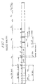
- la Fig. 1 montre schématiquement la structure d'une trame numérique ;
- la Fig. 2 montre schématiquement la structure du champ d'adresse dans une trame ;
- la Fig. 3 montre schématiquement la structure d'une cellule de trame ;
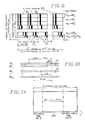
- la Fig. 4 montre en détail la structure d'une cellule du type première cellule de trame ou cellule contenant une trame complète ;
- la Fig. 5 est un bloc-diagramme schématique d'un relais-commutateur de trames conforme à l'invention ;
- la Fig. 6 montre schématiquement la répartition de cellules de trame mémorisées dans la mémoire tampon du relais-commutateur ;
- la Fig. 7 est un bloc-diagramme détaillé d'un bloc de registres d'écriture et d'un bloc de registres de lecture pour la mémoire tampon, inclus dans le relais-commutateur ;
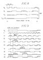
- la Fig. 8 un diagramme temporel montrant l'ensemble des signaux d'adresse de mot de cellule de trame ;
- la Fig. 9 un diagramme temporel montrant des signaux d'horloge produits par une base de temps inclus dans le relais-commutateur ;
- la Fig. 10 montre schématiquement des décalages temporels d'un temps-mot entre des cellules synchronisées provenant de voies d'entrée et appliquées à une matrice de rotation d'entrée incluse dans le relais-commutateur;
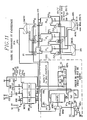
- la Fig. 11 est un bloc-diagramme détaillé d'une unité de commande et d'adressage inclus dans le relais-commutateur ;
- la Fig. 12 est un diagramme temporel montrant des signaux pour mettre à jour des nombres de cellules mémorisées relatives à des trames en cours de mémorisation en mémoire tampon ;
- la Fig. 13 est un diagramme temporel montrant des signaux pour l'incrémentation et la décrémentation de nombres de cellules à retransmettre respectivement vers des voies de sortie du relais-commutateurs ; et
- la Fig. 14 est un schéma concernant la capacité de la mémoire tampon et illustrant une possibilité d'écrasement de cellules.
- Fig. 1 schematically shows the structure of a digital frame;
- Fig. 2 schematically shows the structure of the address field in a frame;
- Fig. 3 schematically shows the structure of a frame cell;
- Fig. 4 shows in detail the structure of a cell of the first frame cell type or cell containing a complete frame;
- Fig. 5 is a schematic block diagram of a frame switch relay according to the invention;
- Fig. 6 schematically shows the distribution of frame cells stored in the buffer memory of the relay-switch;
- Fig. 7 is a detailed block diagram of a block of write registers and a block of read registers for the buffer memory, included in the relay-switch;
- Fig. 8 a time diagram showing all the frame cell word address signals;
- Fig. 9 a time diagram showing clock signals produced by a time base included in the relay-switch;
- Fig. 10 schematically shows time shifts of a time-word between synchronized cells coming from input channels and applied to an input rotation matrix included in the relay-switch;
- Fig. 11 is a detailed block diagram of a control and addressing unit included in the relay-switch;
- Fig. 12 is a time diagram showing signals for updating numbers of stored cells relating to frames in buffer storage courses;
- Fig. 13 is a time diagram showing signals for incrementing and decrementing numbers of cells to be retransmitted respectively to output channels of the relay-switches; and
- Fig. 14 is a diagram relating to the capacity of the buffer memory and illustrating a possibility of overwriting cells.
Préalablement est défini ci-après, à titre d'exemple, le contenu des "cellules de données" constituant des trames numériques que reçoit, commute et transmet un relais-commutateur de trames selon l'invention.Beforehand, the content of the "data cells" constituting digital frames which receive, switch and transmit a frame relay relay switch according to the invention is defined below by way of example.
Dans la suite est adopté un format de trames qui, pour l'essentiel, est schématisé à la Fig. 1. Une trame est établie par un terminal d'un réseau numérique temporel asynchrone RTA dans lequel est inclus le relais-commutateur. Une telle trame est composée d'un champ d'adresses à 4 octets, d'un champ de commande et d'information ayant au moins 2 octets, et d'un champ de séquence de contrôle de trame à deux octets FCS. Chaque trame est découpée en segments de 47 octets, afin d'être transmise dans le réseau RTA ; ainsi, lorsque le nombre d'octets dans le champ de commande et d'information est inférieur à un multiple de 47, la trame est complétée en conséquence par des octets non significatifs.In the following, a frame format is adopted which, for the most part, is shown diagrammatically in FIG. 1. A frame is established by a terminal of an asynchronous digital time network ATR in which the relay-switch is included. Such a frame is composed of a 4-byte address field, a command and information field having at least 2 bytes, and a FCS two-byte frame control sequence field. Each frame is divided into segments of 47 bytes, in order to be transmitted in the RTA network; thus, when the number of bytes in the command and information field is less than a multiple of 47, the frame is completed accordingly with non-significant bytes.
Le champ d'adresse est structuré comme indiqué à la Fig. 2 et comprend un premier octet prédéterminé sans intérêt pour la présente invention, et trois autres octets définissant un identificateur de liaison de données DLI. Cet identificateur est un identificateur logique de connexion, ayant une signification locale. La valeur de cet identificateur est déterminée au moment de l'établissement de la connexion par le terminal devant transmettre la trame, puis par le relais-commutateur traversé par la trame. Il n'est pas nécessaire d'exploiter la totalité des bits de l'identificateur DLI dans chaque relais de trame ; le nombre de bits de l'identificateur exploités détermine la taille d'une mémoire de traduction et d'aiguillage MTA inclus dans le relais.The address field is structured as shown in Fig. 2 and comprises a first predetermined byte of no relevance to the present invention, and three other bytes defining a DLI data link identifier. This identifier is a logical connection identifier, with local meaning. The value of this identifier is determined when the connection is established by the terminal which is to transmit the frame, then by the relay-switch through which the frame passes. It is not necessary to use all the bits of the DLI identifier in each frame relay; the number of bits of the identifier used determines the size of a translation memory and MTA switch included in the relay.
Le champs FCS est une suite de 16 bits permettant, à la réception, de détecter une erreur de transmission.The FCS field is a 16-bit sequence allowing, upon reception, to detect a transmission error.
Chaque segment de 47 octets issu du découpage d'une trame est préalablement inclus dans une cellule de données à 53 octets.Each segment of 47 bytes resulting from the division of a frame is previously included in a data cell with 53 bytes.
Comme montré à la Fig. 3, le format d'une cellule consiste en un en-tête à 5 octets et un champ d'information à 48 octets.As shown in Fig. 3, the format of a cell consists of a 5-byte header and a 48-byte information field.
L'en-tête est, lui-même, structuré en sous-champs, parmi lesquels un champ VPI correspondant aux bits de rang 5 à 12 et un champ VCI correspondant aux bits de rang 13 à 28. Les champs VPI et VCI identifient une liaison temporelle asynchrone. Une cellule ne contenant pas d'information est dite vide, et est signalée par VPI=VCI=0.The header is itself structured in sub-fields, among which a VPI field corresponding to the bits of
Dans le champ d'information d'une cellule, le segment de trame est précédé par un champ d'adaptation ayant un octet. Le champ d'adaptation est structuré en deux sous-champs TC et LG. Le premier sous-champ TC comprend deux bits de type de cellule prenant les valeurs suivantes :
- "10" pour une première cellule BOM d'une trame,
- "00" pour une cellule COM intermédiaire entre les premières et dernières cellules d'une trame,
- "01" pour une cellule EOM de fin d'une trame, et
- "11" pour une cellule SSM contenant une trame complète.
- "10" for a first BOM cell of a frame,
- "00" for a COM cell intermediate between the first and last cells of a frame,
- "01" for an EOM cell at the end of a frame, and
- "11" for an SSM cell containing a complete frame.
Le second sous-champ LG a 6 bits qui sont significatifs dans les cellules EOM et SSM et qui indique le nombre d'octets utiles dans la cellule.The second LG subfield has 6 bits which are significant in the EOM and SSM cells and which indicates the number of useful bytes in the cell.
Quand la segmentation est effectuée sur une trame, la première cellule BOM ou SSM d'une trame contient, comme montré à la Fig. 4, les champs VPI, VCI, TC, LG et DLI, qui sont les seuls champs exploités par le relais-commutateur de trames.When segmentation is performed on a frame, the first BOM or SSM cell of a frame contains, as shown in Fig. 4, the VPI, VCI, TC, LG and DLI fields, which are the only fields used by the frame relay-switch.
Comme montré schématiquement à la Fig. 5, le relais-commutateur de trames comprend essentiellement un étage d'entrée EE, une mémoire tampon MT, un étage de sorties ES, une unité de commande et d'adressage UCA, un processeur de commande de commutation PCC et une base de temps BT.As shown schematically in FIG. 5, the frame relay-switch essentially comprises an input stage EE, a buffer memory MT, an output stage ES, a control and addressing unit UCA, a switching control processor PCC and a time base BT.
Le relais commute des trames sous forme de cellules entre I voies d'entrée numériques temporelles asynchrones VEO à VEI-1 et I voies de sorties temporelles asynchrones VSO à VSI-1. Les trames entrantes dans les voies d'entrée comme les trames sortantes dans les voies de sortie ne sont par entrelacées. En d'autres termes, dans une voie d'entrée ou de sortie, les cellules d'une trame ne sont pas séparées par les cellules d'une autre trame ; toutes les cellules d'une trame arrivent jointives au relais de trames, c'est-à-dire ne sont pas séparées par des cellules vides.The relay switches frames in the form of cells between I asynchronous digital time input channels VE O to VE I -1 and I asynchronous time output channels VS O to VS I -1. Incoming frames in the input channels like outgoing frames in the output channels are not interleaved. In other words, in a route of entry or output cells of a frame are not separated by cells of another frame; all the cells of a frame arrive contiguous to the frame relay, that is to say are not separated by empty cells.
L'étage d'entrée EE a pour rôle d'orienter les données TC et DLI d'une trame qui participe à la fonction de relais, vers l'unité de commande et d'adressage UCA et d'appliquer en écriture des informations résiduelles de chaque trame en mémoire tampon MT. L'unité UCA a pour rôle de déterminer la voie de sortie d'une trame en fonction des informations TC et DLI. L'étage de sortie ES est chargé de transmettre une trame sur la voie de sortie vers laquelle elle a été relayée.The role of the input stage EE is to direct the TC and DLI data of a frame which participates in the relay function, towards the control and addressing unit UCA and to apply in writing residual information. of each frame in MT buffer. The role of the UCA unit is to determine the output channel of a frame as a function of the TC and DLI information. The output stage ES is responsible for transmitting a frame on the output channel to which it has been relayed.
Dans la suite, on considère que le nombre I de voies d'entrée et le nombre I de voies de sortie sont égaux à 16. Ce nombre pourrait, tout aussi bien, être égal à une puissance de 2 inférieure, par exemple 2, 4, ou 8, sans remise en cause de l'organisation du relais-commutateur de trames ; la seule conséquence serait de diminuer les contraintes temporelles. Comme déjà dit, une cellule comprend 53 octets ; cependant pour simplifier la réalisation du relais, chaque cellule est agrandie à 56 octets, ce qui permet de considérer qu'une cellule est composée de R = 16 mots de 28 bits m₀ à m₁₅. En conséquence, les (16 x 28)(6 + 47) 8 = 24 dernier bits dans le dernier mot m₁₅ sont sans signification, et seuls les quatre premiers bits de ce dernier mot sont significatifs, comme montré à la Fig. 6.In the following, we consider that the number I of input channels and the number I of output channels are equal to 16. This number could just as easily be equal to a power of 2 less, for example 2, 4 , or 8, without calling into question the organization of the frame switch relay; the only consequence would be to reduce the time constraints. As already said, a cell has 53 bytes; however, to simplify the implementation of the relay, each cell is enlarged to 56 bytes, which makes it possible to consider that a cell is composed of R = 16 words of 28 bits m₀ to m₁₅. Consequently, the (16 x 28) (6 + 47) 8 = 24 last bits in the last word m₁₅ are meaningless, and only the first four bits of this last word are significant, as shown in Fig. 6.
La base de temps BT comprend classiquement une horloge locale HL à une fréquence multiple entière du débit binaire dans les voies d'entrée et de sortie. A partir de cette horloge locale et au moyen de diviseurs de fréquence, de compteurs et de circuits logiques simples DCT, la base de temps établit de nombreux signaux d'horloge nécessaires aux diverses fonctions du relais-commutateur. Ces signaux sont des signaux principaux H₀ à HQ+M-1 qui définissent des adresses de mot dans la mémoire tampon MT, et des signaux secondaires de fréquence plus grande qui commandent notamment les écritures et lectures de mot et de partie de mot.The time base BT conventionally comprises a local clock HL at an integral multiple frequency of the bit rate in the input and output channels. From this local clock and by means of frequency dividers, counters and simple DCT logic circuits, the time base establishes numerous clock signals necessary for the various functions of the relay-switch. These signals are main signals H₀ to H Q + M-1 which define word addresses in the buffer memory MT, and secondary signals of greater frequency which in particular control the writing and reading of word and part of a word.
Comme montré à la Fig. 7, la mémoire tampon MT est composée de R = 16 sous-mémoires identiques et indépendantes MT₀ à MT₁₅. Une sous-mémoire MTr, où r est en indice entier compris entre 0 et R - 1 = 15, est destinée à stocker les mots mr ayant le rang r dans toutes les cellules. Chaque mot est appliqué sous la forme de 28 bits parallèles pour être écrit dans la mémoire à travers un bus respectif à 28 fils BMEr , et de même, est lu pour être transmis sous la forme de 28 bits parallèles dans un bus respectif de sortie à 28 fils BMSr.As shown in Fig. 7, the buffer memory MT is composed of R = 16 identical and independent sub-memories MT₀ to MT₁₅. A sub-memory MT r , where r has an integer index between 0 and R - 1 = 15, is intended to store the words m r having the rank r in all cells. Each word is applied in the form of 28 parallel bits to be written into the memory through a respective 28-wire bus BME r , and likewise, is read to be transmitted in the form of 28 parallel bits in a respective output bus. with 28 wires BMS r .
Si H₀ est un signal d'horloge dont la demi-période définit un "temps-mot" tm, c'est-à-dire l'intervalle de temps occupé par un mot à 28 bits, il apparaît que Q = 4 signaux d'horloge en phase H₀, H₁, H₂ HQ-1 = H₃ ayant des périodes respectives 2 tm, 4 tm, 8 tm, 2Q tm sont nécessaires pour écrire 1 = 2Q = 16 mots provenant des I voies VE₀ à VEI-1, successivement dans chaque sous-mémoire, et comme on le verra dans la suite, pour écrire les R = 16 mots d'une même cellule respectivement dans les sous-mémoires MT₀ à MT₁₅. Les signaux H₀ à H₃, désignés ensemble par BT0, sont montrés à la Fig. 8 et déterminent ainsi les adresses des sous-mémoires et aussi les adresses des voies d'entrée VE₀ à VE₁₅ dans chacune des sous-mémoires.If H₀ is a clock signal whose half-period defines a "word-time" tm, that is to say the time interval occupied by a 28-bit word, it appears that Q = 4 signals d clock in phase H₀, H₁, H₂ H Q-1 = H₃ having
Selon le schéma de la Fig. 6, les cellules sont stockées obliquement dans les sous-mémoires MT₀ à M₁₅ sous une forme sensiblement parallèle et diagonale, dite "paragonale", comme décrit dans la EP-A-O 113 639. Chaque sous-mémoire MTO à MT₁₅ contient ainsi N blocs de I = 16 mots à 28 bits parallèles, où l'entier N définit la capacité de la mémoire tampon MT en fonction du nombre de cellules moyen par trame et du taux de perte de cellule par voie d'entrée, et donc la capacité de la mémoire à stocker des trames. Pour repérer ces N blocs, la base de temps BT établit M autres signaux d'horloge hQ à HQ+M-1 ayant des périodes (2Q+M tm) = 32 à (2Q+M tm) respectivement désignées ensemble par BT1 dans la suite. Les signaux BTO et BT1 constituent ainsi l'adresse d'écriture d'un mot à 28 bits dans une sous-mémoire MTr.According to the diagram in FIG. 6, the cells are stored obliquely in the sub-memories MT₀ to M₁₅ in a substantially parallel and diagonal form, called "paragonal", as described in EP-AO 113 639. Each sub-memory MT O to MT₁₅ thus contains N blocks of I = 16 words with 28 parallel bits, where the integer N defines the capacity of the buffer memory MT as a function of the average number of cells per frame and the rate of cell loss per input channel, and therefore the capacity of the memory to store frames. To locate these N blocks, the time base BT establishes M other clock signals h Q to H Q + M-1 having periods (2 Q + M tm) = 32 to (2 Q + M tm) respectively designated together. by BT1 below. The signals BTO and BT1 thus constitute the address for writing a 28-bit word in a sub-memory MT r .
Comme montré à la Fig. 9, en dépendance d'un signal d'horloge maître h ayant une demi-période égale à tm/8, la base de temps BT fournit des signaux d'horloge kl et kO de période tm/4 respectivement en phase avec les fronts montants et descendants du signal h, des signaux d'horloge h1 et h0 de demi-période tm/2 respectivement en phase avec des fronts descendants de rangs impairs et pairs du signal h, ainsi que des signaux ![]()
![]()
![]()
![]()
![]()
![]()
![]()
![]()
Ainsi, chaque temps-mot tm est décomposé en deux temps dévolus, l'un à la lecture en mémoire tampon et correspondant à h2 = "0", et l'autre à l'écriture et correspondant à h2 = "1". Pour chaque sous-mémoire MTr, un multiplexeur MXTr sélectionne, sous la commande du signal h2, l'adresse d'écriture ou de lecture. Le signal k1.h2 commande plus précisément l'écriture.Thus, each word-time tm is broken down into two devolved times, one for reading in buffer memory and corresponding to h2 = "0", and the other for writing and corresponding to h2 = "1". For each sub-memory MT r , a multiplexer MXT r selects, under the control of the signal h2, the write or read address. The signal k1.h2 more precisely controls the writing.
D'autres signaux résultant d'opérations logiques simples sur les signaux d'horloge sont également produits, comme montrés aux Figs. 12 à 14, et leur rôle sera justifié dans la suite.Other signals resulting from simple logic operations on the clock signals are also produced, as shown in Figs. 12 to 14, and their role will be justified below.
Comme montré aux Figs. 5 et 7, l'étage d'entrée EE comprend I = 16 interfaces d'entrée IE₀ à IE₁₅ respectivement reliées aux voies VE₀ à VE₁₅, un circulateur MRE et un bloc de registres d'écriture BRE.As shown in Figs. 5 and 7, the input stage EE comprises I = 16 input interfaces IE₀ to IE₁₅ respectively connected to the channels VE₀ to VE₁₅, a circulator MRE and a block of write registers BRE.
Le rôle d'un interface d'entrée IEi est d'assurer la synchronisation du début de cellule et la synchronisation du début de trame en fonction des signaux BT0, et la parallélisation des cellules dans la voie VEi en des mots à 28 bits parallèles dans un bus BEi.The role of an IE i input interface is to ensure the synchronization of the cell start and the synchronization of the start of the frame as a function of the BT0 signals, and the parallelization of the cells in the VE i channel into 28-bit words parallel in a BE bus i .
La synchronisation de cellule consiste à détecter le début d'une cellule dans le flux de bits sérialisées arrivant dans la voie d'entrée VEi Pour cela est utilisé un champ de contrôle d'erreur d'en-tête à 8 bits HEC, les bits du champ HEC correspondant aux bits 33 à 40 (Fig. 4) contenus dans l'en-tête de chaque cellule. Dans le principe, la synchronisation de cellule est déclarée acquise quand le calcul du syndrome sur les 40 bits courants de l'en-tête de cellule donne un résultat nul.Cell synchronization consists in detecting the start of a cell in the serialized bit stream arriving in the input channel VE i For this, an 8-bit HEC header error control field is used, the bits of the HEC field corresponding to
La synchronisation de trame consiste à retrouver le début d'une trame dans le flux de cellules sérialisées arrivant dans la voie VEi. On sait que la première cellule d'une trame a un code TC = "10" pour une cellule BOM, et TC = "11" pour une cellule SSM. A partir du code TC s'effectue la recherche de début de trame. Quand le début d'une trame est détecté, un calcul du syndrome de la trame est déclenché. Ce calcul ne prend en compte ni les en-têtes de cellule ni les champs d'adaptation TC + LG. De plus, seuls les octets significatifs d'une cellule de fin de trame EOM ou SSM, dont leur nombre est indiqué par le champ LG, entrent dans le calcul du syndrome. A la fin du calcul, après les LG octets significatifs d'une cellule EOM ou SSM, la synchronisation de trame est acquise lorsque le résultat du calcul est nul. Dans le cas contraire, une erreur est détectée, à la suite, par exemple, d'une erreur de transmission, ou d'une perte ou d'un gain de cellule.Frame synchronization consists in finding the start of a frame in the flow of serialized cells arriving in the path VE i . We know that the first cell of a frame has a code TC = "10" for a BOM cell, and TC = "11" for an SSM cell. From the TC code, the start of the frame is carried out. When the start of a frame is detected, a calculation of the frame syndrome is triggered. This calculation does not take into account the cell headers or the TC + LG adaptation fields. In addition, only the significant bytes of an EOM or SSM end-of-frame cell, the number of which is indicated by the LG field, are included in the calculation of the syndrome. At the end of the calculation, after the significant LG bytes of an EOM or SSM cell, the frame synchronization is acquired when the result of the calculation is zero. Otherwise, an error is detected, subsequently, by example, a transmission error, or a cell loss or gain.
Chaque cellule sérialisée dans la voie VEi est mise en parallèle sur 28 bits et mémorisée dans un convertisseur série-parallèle et dans une file FIFO inclus dans l'interface IEi. Chaque fois qu'un mot HEC est détecté, l'information de début de cellule sous la forme d'un bit à état prédéterminé di est également mémorisée dans la file. Si une erreur est détectée lors de la validation de la séquence de contrôle de trame FCS inclus dans les deux derniers octets significatifs de la dernière cellule EOM ou SSM de la trame courante, la dernière cellule n'est pas écrite dans la file. L'absence de la dernière cellule de la trame sera exploitée par l'unité de commande et d'adressage UCA pour ne pas retransmettre cette trame.Each cell serialized in the VE i channel is put in parallel on 28 bits and stored in a serial-parallel converter and in a FIFO queue included in the IE i interface. Each time an HEC word is detected, the cell start information in the form of a predetermined state bit d i is also stored in the queue. If an error is detected during the validation of the FCS frame control sequence included in the last two significant bytes of the last EOM or SSM cell of the current frame, the last cell is not written to the queue. The absence of the last cell of the frame will be exploited by the control and addressing unit UCA so as not to retransmit this frame.
Il apparaît ainsi que les interfaces d'entrée IE₀ à IE₁₅ ont des fonctions quelque peu similaires à celles des circuits d'entrée CE₀ à CE₁₅ décrits dans la EP-A-0113639, afin de synchroniser entre elles les cellules et trames respectivement dans les voies d'entrée VE₀ à VE₁₅, et les décaler temporellement les unes par rapport aux autres, d'un temps-mot tm, comme montré à la Fig. 10. Ce décalage temporel résultant d'une conversion parallèle-diagonale impose que les mots de même rang Mr dans des cellules synchrones transmis par les bus BEO à BE₁₅ soient décalés les uns par rapport aux autres du temps-mot tm. Le décalage temporel est commandé par un démultiplexeur d'aiguillage AIG, dont l'entrée de données est à l'état "1", et les entrées de sélection reçoivent les adresses BTO à la période tm pour établir les I = 16 signaux logiques respectivement rythmant la lecture des files FIFO dans les interfaces IE₀ à IE₁₅.It thus appears that the input interfaces IE₀ to IE₁₅ have functions somewhat similar to those of the input circuits CE₀ to CE₁₅ described in EP-A-0113639, in order to synchronize the cells and frames respectively in the channels input VE₀ to VE, and shift them in time relative to each other, by a word time tm, as shown in FIG. 10. This time shift resulting from a parallel-diagonal conversion requires that the words of the same rank M r in synchronous cells transmitted by the buses BE O to BE₁₅ be offset with respect to each other by the time-word tm. The time shift is controlled by an AIG routing demultiplexer, the data input of which is in state "1", and the selection inputs receive the BTO addresses at the period tm to establish the I = 16 logic signals respectively punctuating the reading of FIFO files in the interfaces IE₀ to IE₁₅.
En référence à la Fig. 7, les bus BE₀ à BE₁₅ ayant 28 fils relient respectivement les sorties des files FIFO dans les interfaces IEO à IE₁₅ à des ports d'entrée du circulateur MRE qui est une matrice de rotation. Cette matrice multiplexe les mots à 28 bits parallèles de même rang m₀ à m₁₅ dans les cellules synchrones décalées temporellement, dans les bus BME₀ à BME₁₅. Si r désigne le rang d'un mot dans une cellule et i le rang de la voie d'entrée VEi et du bus BEi, où i et r sont des entiers compris entre 0 et 15, le mot mr de rang r d'une cellule transmise par le bus BEi sort de la matrice MRE par le bus BMEr en même temps que sortent par le bus BMEi le mot mi de rang i d'une cellule transmise par le bus BEr, et par le bus BME₀ le mot m₀de rang 0 d'une cellule transmise par le bus BEi+r . En particulier, il est à noter que le champ de liaison temporelle asynchrone à 24 bits VPI + VCI est transmis par le premier bus BME₀, le champ de type de cellule TC à 2 bits est transmis par le second bus BME₁, et le champ d'identification de liaison DLI à 3 octets est transmis par le troisième bus BME₂.With reference to FIG. 7, the buses BE₀ to BE₁₅ having 28 wires respectively connect the outputs of the FIFO queues in the interfaces IE O to IE₁₅ to input ports of the circulator MRE which is a rotation matrix. This matrix multiplexes the 28-bit parallel words of the same rank m₀ to m₁₅ in the time-shifted synchronous cells, in the buses BME₀ to BME₁₅. If r denotes the rank of a word in a cell and i the rank of the input channel VE i and of the bus BE i , where i and r are integers between 0 and 15, the word m r of rank r of a cell transmitted by the BE bus i leaves the MRE matrix by the BME bus r at the same time as the word m i of rank i leaves a cell transmitted by the bus BE r via the BME bus i , and by the BME₀ bus the
En l'absence du bloc de registres d'écriture BRE, 16 mots de rangs différents et de cellules différentes sont écrits à chaque temps-mot en mémoire tampon, à l'adresse indiquée par le couple (BTO, BT1).In the absence of the block of write registers BRE, 16 words of different ranks and of different cells are written at each word-time in buffer memory, at the address indicated by the pair (BTO, BT1).
Par rapport à une cellule donnée en sortie de la matrice d'entrée MRE, le mot m₀ de la cellule se trouve sur le bus BME₀ au temps tm₀, et le mot mr se trouve sur le bus BMEr au temps tmr. Les informations nécessaires au traitement d'une trame se trouvent dans les mots m₁ et m₂ d'une cellule qui sont alors respectivement retardés de deux temps-mot dans des registres en séries TP0 et TP1 et d'un temps-mot dans un registre TP2 . Ces trois registres possèdent chacun 28 étages parallèles et reçoivent le signal d'horloge h2. Au troisième temps-mot suivent :
Les 24 bits dans les mots VPI et VCI à la sortie du registre TP1 sont décodés par un détecteur de cellule vide DCV sous la forme d'un circuit OU pour déterminer si la cellule est vide, auquel cas le traitement de la cellule est désarmé, en appliquant un signal CNV = "0" à une entrée de validation d'un décodeur de 2 bits DEC.- Les deux bits du mot de type de cellule TC, aux rangs 41
et 42 dans la cellule, sont transmis par le registre TP2 et décodés par le décodeur DEC en un signal "1" sur l'une parmi quatre sorties SB, SS, SC et SE du décodeur DEC, correspondant aux cellules BOM, SSM, COM et EOM lorsque le décodeur DEC est activé par CNV = "1" ; les sorties SB et SS du décodeur DEC sont liées à deux entrées d'une porte OU, PBS, qui fournit un signal DT à l'état "1" pour signaler un début de trame, et les sorties SS et SE du décodeur DEC sont reliées à deux entrées d'une porte OU, PCE, qui fournit un signal FT à l'état "1" pour signaler une fin de trame ; la sortie SC du décodeur DEC est reliée à des entrées inverses des portes PBS et PCE. - Le nouveau mot m₂ de la cellule est déterminé : si on suppose que les deux premiers octets DLIE du champ DLI sont utilisés, les octets DLIE sont transmis à une mémoire de traduction MTA (Fig. 5) qui les remplace par une nouvelle valeur DLIS lorsque la cellule est du type "première" BOM ou SSM, ou les octets DLIE demeurent inchangés lorsque la cellule n'est pas du type "première". Ces dernières opérations sont réalisées par un multiplexeur MXT dont des premières entrées sont reliées au bus BME₂ et des secondes entrées sont reliées à seize sorties DLIS de la mémoire MTA et aux douze derniers fils du bus BME₂ ; ces premières et secondes entrées sont sélectionnées par le signal de début de trame DT.
- The 24 bits in the words VPI and VCI at the output of the register TP1 are decoded by an empty cell detector DCV in the form of an OR circuit to determine whether the cell is empty, in which case the processing of the cell is disarmed, by applying a signal CNV = "0" to a validation input of a 2-bit DEC decoder.
- The two bits of the cell type word TC, at
ranks - The new word m₂ of the cell is determined: if we assume that the first two DLIE bytes of the DLI field are used, the DLIE bytes are transmitted to an MTA translation memory (Fig. 5) which replaces them with a new DLIS value when the cell is of the "first" BOM or SSM type, or the DLIE bytes remain unchanged when the cell is not of the "first" type. These latter operations are carried out by an MXT multiplexer, the first inputs of which are connected to the BME₂ bus and the second inputs of which are connected to sixteen DLIS outputs of the MTA memory and to the last twelve wires of the BME₂ bus; these first and second inputs are selected by the start of frame signal DT.
Les trois mots m₀, m₁ et m₂ de la même cellule donnée sont alors écrits en sous-mémoires MT₀, MT₁ et MT₂ à l'adresse donnée par la valeur courante de (BT0, BT1). Au temps-mot suivant, le mot m₃ de ladite cellule, est écrit en sous-mémoire MT₃ à l'adresse (BT0, BT1) + 1 (mod 16N), etc. La cellule est rangée en mémoire tampon tel qu'indiqué à la Fig. 6.The three words m₀, m₁ and m₂ of the same given cell are then written in sub-memories MT₀, MT₁ and MT₂ at the address given by the current value of (BT0, BT1). At the next word time, the word m₃ of said cell, is written in sub-memory MT₃ at the address (BT0, BT1) + 1 (mod 16N), etc. The cell is stored in buffer memory as shown in FIG. 6.
L'organisation schématique de l'unité de commande et d'adressage UCA est indiquée dans la Fig. 5. Les éléments fonctionnels et essentiels de cette unité UCA sont la mémoire de traduction et d'aiguillage MTA, une mémoire de contexte MCTX, des files d'adresses de voie de sortie FS₀ et FS₁₅ et un circuit de contrôle d'état de file de sortie CEFS.The schematic organization of the UCA control and addressing unit is shown in Fig. 5. The functional and essential elements of this UCA unit are the translation and routing memory MTA, a context memory MCTX, output channel address queues FS₀ and FS₁₅ and a queue status control circuit. CEFS output.
La mémoire de traduction et d'aiguillage MTA montrée à la Fig. 5 est une mémoire RAM contenant (16.2Y) mots de liaison DLIS. L'entier y est inférieur à (8 - 1) x 2 = 14 et désigne le nombre de bits utiles dans un mot DLIE transmis dans le bus BME₂, comme montré à la Fig. 4. A chaque mot DLIE déterminant une adresse d'écriture en combinaison avec l'adresse BTO de la voie d'entrée VE₀ à VE₁₅ à chaque temps-mot tm correspond un nouveau mot de liaison à 16 bits DLIS lu dans la mémoire MTA et associé avec un numéro à 4 bits NVS de la voie de sortie VS₀ à VS₁₅ que doit emprunter la trame dans laquelle est incluse la cellule courante. Le nouveau mot DLIS est appliqué aux secondes entrées du multiplexeur MXT pour être écrit dans la sous-mémoire MT2, et le numéro NVS est fourni à une première "colonne"de la mémoire de contexte MCTX.The MTA translation and referral memory shown in FIG. 5 is a RAM memory containing (16.2Y) DLIS link words. The integer y is less than (8 - 1) x 2 = 14 and designates the number of useful bits in a DLIE word transmitted in the BME₂ bus, as shown in FIG. 4. Each DLIE word determining a write address in combination with the BTO address of the input channel VE₀ to VE₁₅ at each time-word tm corresponds a new 16-bit link word DLIS read in the memory MTA and associated with a 4-bit NVS number of the output channel VS₀ to VS₁₅ to be used by the frame in which the current cell is included. The new word DLIS is applied to the second entries of the MXT multiplexer to be written in the sub-memory MT2, and the NVS number is supplied to a first "column" of the context memory MCTX.
La mémoire de traduction et d'aiguillage MTA est mise à jour par le processeur de commande PCC lors de l'établissement d'une liaison.The translation and routing memory MTA is updated by the control processor PCC when a connection is established.
La mémoire de contexte MCTX contient seize triplets déterminant seize contextes respectivement associés aux trames en cours de traitement reçues par les seize voies d'entrée VE₀ à VE₁₅, et adressés cycliquement par les mots BT0.The context memory MCTX contains sixteen triples determining sixteen contexts respectively associated with the frames being processed received by the sixteen input channels VE₀ to VE₁₅, and addressed cyclically by the words BT0.
Ainsi, à chaque trame en cours de réception, comme montré à la Fig. 11, correspond un contexte incluant le numéro de la voie de sortie NVS à 4 bits lu dans le mémoire MTA, l'adresse AdPC du bloc de la sous-mémoire MT₀ où est écrit la première cellule de la trame, et le nombre NbC des cellules de la trame écrites en mémoire tampon MT. On suppose, à titre d'exemple selon la réalisation illustrée aux Figs. 6 et 11, que la mémoire tampon a une capacité de 2M = 2¹⁰ cellules par voie d'entrée, ce qui conduit à des mots d'adresse d'écriture AdPC déduits des 10 bits de BT1, et que le nombre maximum NC de cellules dans une trame est égal à 2⁶ = 64 < 2M, soit 6 bits pour coder le nombre NbC. Les deux premières colonnes de la mémoire MCTX assignées aux nombres NVS et aux adresses AdPC sont commandées en écriture (E) au début des trames par un signal DT.h1 produit par une porte ET à deux entrées PX1. La troisième colonne de la mémoire MCTX assignée aux nombres NbC est commandée en écriture par un autre signal logique ![]()
![]()
Le nombre NbC est mis à jour au moyen d'un registre d'incrémentation à 6 bits parallèles REG qui incrémente d'une unité le nombre NbC lu en réponse à une cellule de la trame en cours de réception. Le registre REG offre une entrée de remise à zéro RAZ commandé par le signal DT. ![]()
![]()
R = 16 files de sortie FIF0, FS₀ à FS15 , sont respectivement associées aux voies de sortie VS₀ à VS₁₅. Une file de sortie FSi mémorise les adresses à 10 bits AdPC de première cellule des trames qui ont été complètement écrites en mémoire tampon et qui sont destinées à la voie VSi, et quine sont pas complètement lues. Les files FS₀ à FS₁₅ ont des bus d'entrée de données reliées aux 10 sorties de la seconde colonne AdPC de la mémoire de contexte MCTX, et aux 4 sorties BT₀ de la base de temps. Des bus de sortie à 14 fils des files FS₀ à FS₁₅ sont reliés à un multiplexeur d'adresse de lecture MUXL ayant un bus de sortie à 14 fils SFC, et sont sélectionnés cycliquement par les mots BTO dans le multiplexeur MUXL.R = 16 output queues FIF0, FS₀ to FS 15 , are respectively associated with the output channels VS₀ to VS₁₅. An output queue FS i stores the 10-bit AdPC addresses of the first cell of the frames which have been completely written in buffer memory and which are intended for the channel VS i , and which are not completely read. The queues FS₀ to FS₁₅ have data input buses connected to the 10 outputs of the second column AdPC of the context memory MCTX, and to the 4 outputs BT₀ of the time base. 14-wire output buses from lines FS₀ to FS₁₅ are connected to a MUXL read address multiplexer having an SFC 14-wire output bus, and are selected cyclically by the words BTO in the MUXL multiplexer.
Les files FS₀ à FS₁₅ sont commandées en écriture (E) par un démultiplexeur DMUXE recevant des mots NVS à 4 bits lus dans la première colonne de la mémoire MCTX, et par I=16 portes ET à trois entrées PEF₀ à PEF₁₅ ayant des premières entrées reliées respectivement aux I sorties du démultiplexeur DMUXE. Des secondes entrées des portes PEF₀ à PEF₁₅ reçoivent le signal de fin de trame FT. Des troisièmes entrées des portes PEF₀ à PEF₁₅ reçoivent un signal de validation d'écriture VALE du circuit de contrôle CEFS.The files FS₀ to FS₁₅ are commanded in writing (E) by a DMUXE demultiplexer receiving 4-bit NVS words read in the first column of the memory MCTX, and by I = 16 doors AND with three inputs PEF₀ to PEF₁₅ having first inputs connected respectively to the I outputs of the DMUXE demultiplexer. Second inputs of the doors PEF₀ to PEF₁₅ receive the end of frame signal FT. Third inputs of the doors PEF₀ to PEF₁₅ receive a write validation signal VALE from the CEFS control circuit.
Les adresses AdPC + BT0 lues dans les files FS₀ à FS₁₅ sont multiplexées dans un multiplexeur MUXL. La lecture des files est commandée par I = 16 portes ET à quatre entrées PLF₀ à PLF₁₅ ayant des premières entrées directes reliées respectivement aux I sorties d'un démultiplexeur DMUXL. Des secondes entrées inverses des portes PLF₀ à PLF₁₅ reçoivent un signal de trame ST qui est à l'état "1" tant qu'une trame est en cours de lecture pendant le temps-mot cyclique correspondant à la file et la voie associées. Des sorties des files FS₀ à FS₁₅ appliquent à des troisièmes entrées directes des portes PLF₀ à PLF₁₅, des signaux FNV₀ à FNV₁₅, qui sont chacun à l'état "1" tant que la file associée n'est pas vide et donc contient au moins une adresse de première cellule. Enfin, des quatrièmes entrées directes des portes PLF₀ à PLF₁₅ reçoivent le signal logique h2 afin de lire l'une des files FS₀ à FS₁₅ pendant une opération d'écriture dans la mémoire tampon.The AdPC + BT0 addresses read from the queues FS₀ to FS₁₅ are multiplexed in a MUXL multiplexer. The reading of the queues is controlled by I = 16 doors AND with four inputs PLF₀ to PLF₁₅ having first direct inputs connected respectively to the I outputs of a DMUXL demultiplexer. Second reverse inputs of the doors PLF₀ to PLF₁₅ receive a frame signal ST which is in the state "1" as long as a frame is being read during the cyclic word time corresponding to the queue and the associated channel. Outputs of the queues FS₀ to FS₁₅ apply to third direct inputs of the doors PLF₀ to PLF₁₅, signals FNV₀ to FNV₁₅, which are each in the state "1" as long as the associated queue is not empty and therefore contains at least a first cell address. Finally, fourth direct inputs from the doors PLF₀ to PLF₁₅ receive the logic signal h2 in order to read one of the queues FS₀ to FS₁₅ during a write operation in the buffer memory.
Le circuit de contrôle d'état de file de sortie CEFS contient une mémoire MEFS stockant I = 16 nombres NbCRT₀ à NBCRT₁₅ de cellules à retransmettre respectivement vers les voies de sortie VS₀ à VS₁₅ et donc des nombres associés aux files de sortie FS₀ à FS₁₅ . Comme les adresses BT1, les nombres NbCRT₀ à NbCRT₁₅ sont limités par le nombre de cellules pouvant être écrites en mémoire tampon MT et provenant d'une même voie d'entrée, et sont donc limités à N=2M=2¹⁰. La mémoire MEFS est adressée alternativement pendant un temps-mot tm, par le numéro de voie courant NVS lu en mémoire MCTX, en réponse à h2 = "0", et par le numéro de voie d'entrée BT0, en réponse à h2 = "1", à travers un multiplexeur MX1a.The output queue status control circuit CEFS contains a MEFS memory storing I = 16 numbers NbCRT₀ to NBCRT₁₅ of cells to be retransmitted respectively to the output channels VS₀ to VS₁₅ and therefore numbers associated with the output queues FS₀ to FS₁₅. Like the addresses BT1, the numbers NbCRT₀ to NbCRT₁₅ are limited by the number of cells that can be written in buffer MT and coming from the same input channel, and are therefore limited to N = 2 M = 2¹⁰. The MEFS memory is addressed alternately for a word time tm, by the current channel number NVS read in memory MCTX, in response to h2 = "0", and by the input channel number BT0, in response to h2 = "1", through a multiplexer MX1a.
Le circuit CEFS comprend également un registre-totaliseur TOT ayant M=10 premières entrées de données reliées au bus de sortie de données de la mémoire MEFS, et six secondes entrées de données reliées au bus de sortie de la troisième colonne NbC de la mémoire de contexte MCTX, à travers des premières entrées d'un multiplexeur MX1b. Six secondes entrées du multiplexeur MX1b sont portées aux états "000001" représentatifs du chiffre 1. Des entrées de sélection des multiplexeurs MX1a et Mx1b et d'un troisième multiplexeur MX1c dans le circuit CEFS, et une entrée de commande d'incrémentation (+) / décrémentation (-) du registre TOT reçoivent le signal h2. L'incrémentation ou la décrémentation sélectionnée dans le registre TOT est validée par un état "1" à une entrée V de ce registre qui est reliée à une sortie du multiplexeur MX1c. Les entrées du multiplexeur MX1c reçoivent le signal k0 et, à travers une porte ET de validation d'incrémentation à deux entrées PI, le signal (k0.FT). Le bus de sortie à 10 fils du registre -totalisateur TOT est relié aux entrées de données de la mémoire MEFS. Dans cette mémoire, l'écriture est commandée par le signal de validation VALE =
Le principe général de fonctionnement de l'unité de commande et d'adressage UCA est le suivant, en référence avec les Figs. 7 et 11.The general operating principle of the control and addressing unit UCA is as follows, with reference to FIGS. 7 and 11.
A chaque temps-mot tm, l'unité UCA reçoit les signaux de type de cellule DT et FT et les bits d'identificateur DLIE de la cellule reçus par les bus BME₁ et BME₂. Les 14 bits significatifs parmi ces 24 bits d'identificateur sont interprétés comme le champ d'identification DLIE d'une trame, si le champ TC a la valeur BOM ou SSM, c'est-à-dire si DT = "1" et FT = "0".
- Si TC = BOM ou SSM, et donc DT = "1" et FT = "0", DLIE est traduit en DLIS qui détermine le numéro de la voie de sortie ; un contexte (NVS+AdPC+NbC) associé à la trame est créé.
- Si TC = COM, et donc DT = FT = " 0 ", le contexte et particulièrement le nombre NbC est mis à jour.
- Si TC = EOM ou SSM, et donc DT = "0" et FT = "1", toutes les cellules de la trame ont été reçues; l'unité UCA décide si la trame peut être retransmise en fonction de son contexte et de l'état d'occupation de la voie de sortie destinataire.
- If TC = BOM or SSM, and therefore DT = "1" and FT = "0", DLIE is translated into DLIS which determines the number of the output channel; a context (NVS + AdPC + NbC) associated with the frame is created.
- If TC = COM, and therefore DT = FT = "0", the context and particularly the NbC number is updated.
- If TC = EOM or SSM, and therefore DT = "0" and FT = "1", all the cells of the frame have been received; the UCA unit decides whether the frame can be retransmitted according to its context and the busy state of the destination output channel.
Ces opérations sont maintenant détaillées. A chaque temps-mot, la valeur de BT0 indique le numéro de la voie d'entrée qui est prise en compte dans l'unité UCA.These operations are now detailed. At each time-word, the value of BT0 indicates the number of the input channel which is taken into account in the UCA unit.
La mémoire de traduction et d'aiguillage MTA (Fig. 5) est adressée à chaque temps-mot par le couple (BT0, DLIE) pour fournir au multiplexeur MXT (Fig.7) la valeur du nouveau mot DLIS qui sera inclus dans la trame en sortie du relais-commutateur de trames, et le numéro de la voie de sortie NVS vers laquelle doit être retransmise la trame. Le nouveau mot DLIS est écrit dans la sous-mémoire tampon MT₂ (Fig. 7).The MTA translation and referral memory (Fig. 5) is sent to each word-time by the pair (BT0, DLIE) to provide the MXT multiplexer (Fig. 7) with the value of the new DLIS word which will be included in the frame at the output of the frame switch relay, and the number of the NVS output channel to which the frame must be retransmitted. The new word DLIS is written in the buffer sub-memory MT₂ (Fig. 7).
Comme déjà dit, à chaque trame en cours de réception est associé un contexte. La valeur BT0 adresse le contexte courant dans la mémoire MCTX. Chaque contexte contient l'adresse de la première cellule de la trame AdPC en mémoire tampon, le nombre NbC de cellules de cette trame déjà reçues, et le numéro NVS de la voie de sortie vers laquelle la trame doit être retransmise.As already said, a context is associated with each frame being received. The value BT0 addresses the current context in the MCTX memory. Each context contains the address of the first cell of the AdPC frame in buffer memory, the number NbC of cells of this frame already received, and the NVS number of the output channel to which the frame is to be retransmitted.
Si la cellule en cours est une première cellule de trame BOM ou SSM, soit DT = "1", un nouveau contexte est créé en écrivant (E) NVS à la valeur lue NVS dans la mémoire MTA et AdPC à la valeur de BT1, en réponse au signal DT.h1, puis le nombre NbC à 1, en réponse au signal ![]()
![]()
Le signal de chargement pour NbC, le signal de remise à zéro pour le registre REG, le signal d'incrémentation, et le signal de transfert de NbC dans la mémoire MCTX relativement au registre REG sont montrés à la Fig. 12. Si la cellule en cours d'écriture est une cellule intermédiaire COM ou une véritable dernière cellule EOM, soit DT ="0", le nombre de cellules NbC est incrémenté d'une unité, à travers l'entrée + 1 du registre REG. La mise à jour du nombre NbC, par l'intermédiaire du registre REG, s'effectue en quatre temps, tel qu'illustré à la Fig. 12 :
- 1) chargement du registre REG avec la valeur de NbC en réponse à l'adresse de la voie correspondante [BT0] ;
- 2) remise à zéro (RAZ) du registre REG si la cellule incidente est de type BOM ou SSM, soit DT = "1" ;
- 3) incrémentation du registre REG, en réponse à h2.k1 ;
- 4) transfert du contenu du registre REG pour l'écrire dans la troisième colonne de la mémoire MCTX.
- 1) loading of the register REG with the value of NbC in response to the address of the corresponding channel [BT0];
- 2) reset to zero (RESET) of the REG register if the incident cell is of the BOM or SSM type, ie DT = "1";
- 3) incrementation of the REG register, in response to h2.k1;
- 4) transfer of the contents of the REG register to write it in the third column of the MCTX memory.
Si la cellule en cours est une dernière cellule de trame EOM ou SSM, soit FT = "1", l'unité UCA doit décider si cette trame peut être transmise dans la voie de sortie correspondante NVS. Cette décision est basée sur la valeur du compte NbC de la trame et du compte NbCRT de la voie de sortie d'indice NVS. L'évolution du compte NbCRT indiquant à tout moment le nombre de cellules qui doivent être transmises vers la voie de sortie NVS et donc qui appartenait à des trames pour lesquelles la décision de transmission a été prise, sera détaillée plus loin.If the current cell is a last EOM or SSM frame cell, ie FT = "1", the UCA unit must decide whether this frame can be transmitted in the corresponding output channel NVS. This decision is based on the value of the NbC account of the frame and the NbCRT account of the NVS index output channel. The evolution of the NbCRT account indicating at any time the number of cells which must be transmitted to the NVS output channel and therefore which belonged to frames for which the transmission decision has been taken, will be detailed below.
On rappelle que la gestion de la mémoire tampon MT est non optimisée, les adresses d'écriture BT0 étant cycliques. A chaque voie d'entrée VE₀ à VE₁₅ correspond une capacité de 2¹⁰ = N places en mémoire tampon. Ces places sont gérées cycliquement en écriture de telle manière qu'une cellule arrivant sur la voie d'entrée VEi et mémorisée à l'adresse k en mémoire tampon sera écrasée N temps-cellule, soit N(16.tm) plus tard, par une cellule arrivant par la même voie d'entrée VEi ; en fait, l'adresse k est l'adresse d'un mot de rang donné de la cellule, de préférence l'adresse du premier mot m₀. Une cellule peut donc attendre au maximum N temps-cellule en mémoire MT avant d'être retransmise. Comme une trame est composée de plusieurs cellules, le mécanisme de prévention d'écrasement doit connaître le temps de séjour de la première cellule de chaque trame en mémoire tampon. La Fig. 14 illustre ce problème.It will be recalled that the management of the buffer memory MT is not optimized, the write addresses BT0 being cyclical. Each input channel VE₀ to VE₁₅ corresponds to a capacity of 2¹⁰ = N places in the buffer memory. These places are managed cyclically in writing so that a cell arriving on the input channel VE i and stored at address k in the buffer memory will be overwritten N cell-time, ie N (16.tm) later, by a cell arriving by the same entry channel VE i ; in fact, the address k is the address of a word of given rank in the cell, preferably the address of the first word m₀. A cell can therefore wait at most N cell time in memory MT before being retransmitted. As a frame is composed of several cells, the overwrite prevention mechanism must know the residence time of the first cell of each frame in the buffer memory. Fig. 14 illustrates this problem.
La première cellule d'une trame ayant (1 - k) cellules et arrivant sur la voie d'entrée VEi est mémorisée à l'adresse k. La dernière cellule de la trame est mémorisée à l'adresse 1. Le compte NbC associé à la trame, qui indique le nombre de cellules reçues de la trame, indique aussi le temps de séjour, exprimé en temps-cellule, de la première cellule de la trame dans la mémoire tampon jusqu'à la mémorisation complète de la trame. Cette première cellule sera donc écrasée au bout de [X = N - (1-k) mod N] temps-cellule après que la dernière cellule ait été mémorisée. Comme on le verra dans la suite, le circuit de contrôle CEFS ne décide de retransmettre la trame que si moins de X cellules doivent préalablement être transmises sur la même voie de sortie VSi, donc si NbC + NbCRT < N. Le signal de débordement de mémoire DEB est affirmé à l'état "1" quand la trame ne peut être transmise ; dans ce cas, le signal de validation d'écriture VALE est "0", et l'adresse AdPC de la trame n'est pas écrite dans la file FSi (Fig. 11).The first cell of a frame having (1 - k) cells and arriving on the input channel VE i is stored at address k. The last cell of the frame is stored at
A chaque voie de sortie correspond une file de sortie. Cette file mémorise les adresses des premières cellules des trames à transmettre dans la voie de sortie. Le fonctionnement de l'unité UCA garantit qu'une trame, dont l'adresse est rangée dans une file de sortie, sera transmise sans risque d'écrasement. L'écriture et la lecture d'adresse AdPC dans les files se déroulent comme ci-après. Les 16 mots BT0 fournis successivement par la base de temps servent d'adresses pour la mémoire de contexte MCTX, en relation avec la voie d'entrée, et donc de compléments aux adresses AdPC écrites dans les files respectives.Each exit channel corresponds to an exit queue. This queue stores the addresses of the first cells of the frames to be transmitted in the output channel. The operation of the UCA unit guarantees that a frame, the address of which is stored in an output queue, will be transmitted without risk of overwriting. The writing and reading of AdPC addresses in the queues takes place as follows. The 16 words BT0 supplied successively by the time base serve as addresses for the context memory MCTX, in relation to the input channel, and therefore as complements to the AdPC addresses written in the respective queues.
A chaque temps-mot BT0, si la cellule reçue est une dernière cellule d'une trame EOM ou SSM indiquée par FT = "1" aux secondes entrées des portes ET PEF₀ à PEF₁₅ et que le circuit CEFS valide la transmission de la trame correspondante par DEB = "0", la porte correspondante PEFi[BT0] est ouverte, et l'adresse de première cellule AdPC[BT0], lue dans la mémoire de contexte est écrite dans la file FSi dont l'indice i est égal en code binaire à NVS[BT0].At each word time BT0, if the cell received is a last cell of an EOM or SSM frame indicated by FT = "1" at the second inputs of the gates AND PEF₀ to PEF₁₅ and the CEFS circuit validates the transmission of the corresponding frame by DEB = "0", the corresponding door PEF i [BT0] is open, and the address of first cell AdPC [BT0], read in the context memory is written in the queue FS i whose index i is equal in binary code to NVS [BT0].
En lecture, les 16 files sont également considérées cycliquement, une par temps-mot. Le mot d'adresse de file BT0, décodé par le démultiplexeur DMUXL, valide l'une des portes PLFi. La file courante FSi est lue si elle n'est pas vide, soit FNVi = "1", et si la trame précédente a été retransmise complètement dans la voie de sortie associé VSi, soit ST = "0".In reading, the 16 queues are also considered cyclically, one per word-time. The queue address word BT0, decoded by the DMUXL demultiplexer, validates one of the PLF gates i . The current queue FS i is read if it is not empty, that is FNV i = "1", and if the previous frame has been completely retransmitted in the associated output channel VS i , that is ST = "0".
Le mot à 14 bits SFC = [AdPC, BT0] lu dans la file FSi est alors appliqué par le multiplexeur MUXL à des premières entrées d'un multiplexeur d'adresses de lecture MXAL inclus dans un bloc de registres de lecture BRL de l'étage de sortie ES (Figs. 5 et 7).The 14-bit word SFC = [AdPC, BT0] read from the queue FS i is then applied by the multiplexer MUXL to the first inputs of a read address multiplexer MXAL included in a register block BRL readout of the output stage ES (Figs. 5 and 7).
Le fonctionnement du circuit de contrôle d'état de file CEFS est décrit ci-après. Chaque mot NbCRTi indique le nombre de cellules devant être retransmises dans la voie de sortie VSi. Comme montré à la Fig. 13, chaque temps-mot tm est divisé en deux demi-périodes définies par le signal h2 et dévolues l'une à l'incrémentation et l'autre à la décrémentation du nombre NbCRTi, respectivement pour h2 = "0" et h2 = "1". Les multiplexeurs MX1a, MX1b et MX1c sélectionnent les entrées à prendre en compte, en fonction de l'état du signal logique h2.The operation of the CEFS queue status control circuit is described below. Each word NbCRT i indicates the number of cells to be retransmitted in the output channel VS i . As shown in Fig. 13, each time-word tm is divided into two half-periods defined by the signal h2 and assigned one to the incrementation and the other to the decrementation of the number NbCRT i , respectively for h2 = "0" and h2 = "1". The multiplexers MX1a, MX1b and MX1c select the inputs to be taken into account, depending on the state of the logic signal h2.
Le nombre NbCRTi est incrémenté en réponse à une dernière cellule EOM ou SSM d'une trame à retransmettre vers la voie de sortie, signalée par FT="1" en entrée de la porte PI et indiquée par l'adresse NVS[BT0] pour lire, à travers le multiplexeur MX1a (h2 = "0"), le nombre NbCRTi associé à la sortie NVS. Dans le registre-totalisateur TOT, NbCRTi et NbC[BT0] sont additionnés, et la somme est comparée au nombre maximum de cellule N. Si la somme des nombres NbCRTi et NbC[BT0] est supérieure à N, la trame est abandonnée ; ce débordement se traduit par DEB = "1" en sortie du registre TOT, et VALE = "0" en sortie de la porte PV, ce qui maintient fermée la porte ET PEFi correspondant à i = NVS[BT0] et, par suite, l'adresse AdPC[BT0] n'est pas écrite dans la file correspondante FSi, et la trame est abandonnée. Dans le cas contraire, la porte PV est ouverte, la somme NbC+NbCRTi est écrite en tant que nouvelle valeur de NbCRTi dans la mémoire MEFS, et l'adresse AdPC est écrite en file FSi.The number NbCRT i is incremented in response to a last EOM or SSM cell of a frame to be retransmitted to the output channel, signaled by FT = "1" at the input of the gate PI and indicated by the address NVS [BT0] to read, through the multiplexer MX1a (h2 = "0"), the number NbCRT i associated with the NVS output. In the totalizing register TOT, NbCRT i and NbC [BT0] are added, and the sum is compared to the maximum number of cell N. If the sum of the numbers NbCRT i and NbC [BT0] is greater than N, the frame is dropped ; this overflow is reflected by DEB = "1" at the output of the TOT register, and VALE = "0" at the output of the PV gate, which keeps the AND gate PEF closed i corresponding to i = NVS [BT0] and, consequently , the AdPC address [BT0] is not written to the corresponding queue FS i , and the frame is dropped. Otherwise, the PV gate is opened, the sum NbC + NbCRT i is written as a new value of NbCRT i in the MEFS memory, and the AdPC address is written in file FS i .
Le nombre NbCRTi est décrémenté de 1 à chaque fois que la file de sortie FSi devient la file courante, soit h2 = "1" sur le multiplexeur MX1a, en considérant qu'une cellule a été transmise en réponse au mot [BTO]i correspondant. Cette décrémentation n'a lieu que tant que le nombre NbCRTi est supérieur à 0.The number NbCRT i is decremented by 1 each time the output queue FS i becomes the current queue, ie h2 = "1" on the multiplexer MX1a, considering that a cell has been transmitted in response to the word [BTO] i corresponding. This decrementation takes place only as long as the number NbCRT i is greater than 0.
Lors de la phase de décrémentation, h2 ="1", le nombre NbCRTi est sélectionné par la valeur de BT0 correspondant à la file de sortie courante FSi, à travers le multiplexeur MX1a, en considérant qu'une cellule a été transmise par le mot correspondant [BTO]i. La décrémentation d'une unité est validée dans le multiplexeur MX1c, afin que le multiplexeur MX1b applique "000001" aux secondes entrées de données du registre TOT. La valeur décrémentée (NbCRTi-1) est alors écrite dans la mémoire MEFS en réponse au signal de validation d'écriture VALE = " 1 " .During the decrementation phase, h2 = "1", the number NbCRT i is selected by the value of BT0 corresponding to the current output queue FS i , through the multiplexer MX1a, considering that a cell has been transmitted by the corresponding word [BTO] i . The decrementing of a unit is validated in the multiplexer MX1c, so that the multiplexer MX1b applies "000001" to the second data entries of the TOT register. The decremented value (NbCRT i -1) is then written in the MEFS memory in response to the write validation signal VALE = "1".
En se reportant à la Fig. 7, l'étage de sortie ES comprend le bloc de registres de lecture de la mémoire tampon BRL, un circulateur MRS et des interfaces de sortie IRS₀ à IRS₁₅.Referring to FIG. 7, the output stage ES comprises the block of read registers of the buffer memory BRL, a circulator MRS and output interfaces IRS₀ to IRS₁₅.
Le bloc de registres de lecture BRL, qui est détaillé à la Fig. 7, est prévu pour fournir les adresses de lecture des cellules à transmettre aux sous-mémoires tampons MT₀ à MT₁₅, et plus précisément, les adresses successives des R = 16 mots m₀ à m₁₅ de chacune des cellules à transmettre respectivement à des secondes entrées des multiplexeurs MXT₀ à MTX₁₅ reliés aux entrées d'adressage des sous-mémoires tampons MT₀ à MT₁₅. Le bloc BRL comprend R = 16 registres tampons de lecture RPL₀ à RPL₁₅ connectés en cascade et dont les bus de sortie à M+Q=14 fils sont reliés respectivement aux secondes entrées des multiplexeurs MXT₀ à MXT₁₅. Aux registres RPL₂ à RPL₁₅ sont respectivement adjoints des registres tampons à un étage T₂ à T₁₅ qui sont connectés en cascade. Une entrée inverse du premier registre T₂ est reliée au second fil du bus de sortie BMS₁ de la seconde sous-mémoire tampon MT₁ qui convoie le bit b₄₂ du sous-champ TC indiquant à l'état "1" une cellule de "fin de trame" EOM ou SSM (Fig. 4). Le dernier registre T₁₅ produit ainsi le signal ST appliqué à une entrée de sélection du registre MXAL et aux secondes entrées inverses des portes PLF₀ à PLF₁₅ (Fig. 11).The BRL read register block, which is detailed in FIG. 7, is provided to supply the read addresses of the cells to be transmitted to the buffer sub-memories MT₀ to MT₁₅, and more precisely, the successive addresses of the R = 16 words m₀ to m₁₅ of each of the cells to be transmitted respectively to second inputs of the multiplexers MXT₀ to MTX₁₅ connected to the addressing inputs of the buffer sub-memories MT₀ to MT₁₅. The BRL block includes R = 16 read buffer registers RPL₀ to RPL₁₅ connected in cascade and whose output buses at M + Q = 14 wires are respectively connected to the second inputs of the multiplexers MXT₀ to MXT₁₅. The registers RPL₂ to RPL₁₅ are respectively associated with one-stage buffer registers T₂ to T₁₅ which are connected in cascade. An inverse input of the first register T₂ is connected to the second wire of the output bus BMS₁ of the second buffer sub-memory MT₁ which conveys the bit b₄₂ of the TC sub-field indicating in state "1" a cell at "end of frame "EOM or SSM (Fig. 4). The last register T₁₅ thus produces the signal ST applied to a selection input of the register MXAL and to the second reverse inputs of the doors PLF₀ to PLF₁₅ (Fig. 11).
Le bus d'entrée du premier registre RPL₀ est relié aux sorties du multiplexeur MXAL , et les bus d'entrée des registres RPL₁ et RPL₂ sont directement reliés aux sorties des registres précédents RPL₀ et RPL₁ respectivement, puisque les mots m₀, m₁ et m₂ d'une cellule ont été écrits simultanément avec une même adresse d'écriture (BT0, BT1) dans les sous-mémoires MT₀, MT₁ et MT₂, grâce aux registres tampons TP0, TP1 et TP2. Les bus d'entrée des autres registres de lecture RPL₃ à RPL₁₅ sont reliés aux sorties des registres précédents RPL₂ à RPL₁₄ à travers des additionneurs d'une unité AD₃ à AD₁₅, respectivement. Le bus de sortie du dernier registre de lecture RPL₁₅ est relié à des secondes entées du multiplexeur MXAL à travers un additionneur ADD du chiffre trois. Dans ces conditions, après 16 temps-mot succédant à l'inscription de l'adresse du premier mot m₀ d'une cellule dans le registre RPL₀ et rythmés par le signal d'horloge h2 appliqué aux registres RPL₀ à RPL₁₅, l'adresse du premier mot d'une seconde cellule consécutive à la cellule précédente dans la même trame est appliquée au registre RPL₀ à travers le multiplexeur MXAL . En effet, il est rappelé que le rangement des cellules dans la mémoire tampon MT n'est pas optimisé et donc que deux cellules consécutives dans une même trame ont des adresses a et b telles que :![]()
![]()
Les mots d'une cellule étant rangés de manière quasiment diagonale en mémoire tampon, comme montré à la Fig. 6, l'adresse des trois premiers mots d'une cellule est égale à l'adresse du dernier mot de la cellule précédente issue de la même voie d'entrée, augmentée du chiffre trois. Dans les bus de sortie à 28 fils BMS₀ à BMS₁₅ des sous-mémoires MT₀ à MT₁₅, les mots m₀ à m₁₅ d'une cellule sont ainsi tous transmis successivement sous forme diagonale. Il en résulte qu'à chaque temps-mot, le bloc BRL lit 16 mots de rangs différents, respectivement dans 16 cellules différentes, à destination de 16 voies de sorties différentes.The words of a cell being stored almost diagonally in buffer memory, as shown in FIG. 6, the address of the first three words of a cell is equal to the address of the last word of the previous cell from the same input channel, increased by the number three. In the 28-wire output buses BMS₀ to BMS₁₅ of the sub-memories MT₀ to MT₁₅, the words m₀ to m₁₅ of a cell are thus all transmitted successively in diagonal form. As a result, at each word time, the BRL block reads 16 words of different ranks, respectively in 16 different cells, destined for 16 different output channels.
On considère la transmission d'une cellule particulière. A un premier temps-mot, le registre RPL₀ contient l'adresse du premier mot m₀ de la cellule ; au temps-mot suivant, cette adresse est transférée dans le registre RPL₁ et constitue l'adresse du deuxième mot m₁. Pour tenir compte du rangement diagonalement temporel d'une cellule en mémoire, lors du transfert d'adresse du registre RPL₂ au registre RPL₃, puis du registre RPLr au registre RPLr+1, jusqu'au registre RPL₁₅, l'adresse est incrémentée d'une unité. On notera que l'additionneur ADD donne l'adresse du premier mot de la cellule suivante issue de la même voie d'entrée.We consider the transmission of a particular cell. At a first word-time, the register RPL₀ contains the address of the first word m₀ of the cell; at the next word-time, this address is transferred to the register RPL₁ and constitutes the address of the second word m₁. To take account of the diagonally temporal arrangement of a cell in memory, during the transfer of address from the register RPL₂ to the register RPL₃, then from the register RPL r to the register RPL r + 1 , up to the register RPL₁₅, the address is incremented of a unit. Note that the adder ADD gives the address of the first word of the next cell from the same input channel.
Le processus de lecture et transmission d'une trame vers une voie de sortie destinataire VSi se déroule comme suit.The process of reading and transmitting a frame to a destination output channel VS i takes place as follows.
Suite à la lecture de la file de sortie FSi, les sorties SFC du multiplexeur MUXL délivrent l'adresse du premier mot m₀ de la première cellule de la trame à transmettre ; ST étant égal à "0", cette adresse est chargée dans le registre RPL₀ pour lire le mot m₀ de la cellule. Puis à chacun des 15 temps-mot suivants, la même adresse est transférée d'un registre de lecture à l'autre pour permettre la lecture des 15 mots suivants de la cellule.Following the reading of the output queue FS i , the SFC outputs of the multiplexer MUXL deliver the address of the first word m₀ of the first cell of the frame to be transmitted; ST being equal to "0", this address is loaded into the register RPL₀ to read the word m₀ of the cell. Then at each of the following 15 time-words, the same address is transferred from one reading register to another to allow the reading of the next 15 words from the cell.
Lors de la lecture du deuxième mot dans la sous-mémoire MT₁, le bit b42 est mémorisé dans le registre T₂. Les états "1" et "0" de ce bit indiquent si la cellule est ou n'est pas la dernière de la trame. Le bit est propagé à chaque temps-mot du registre Ti au registre Ti+1, jusqu'au registre T₁₅. Quand une nouvelle cellule est à transmettre sur la voie de sortie VSi, deux cas se présentent.
- 1) La cellule qui vient d'être transmise était la dernière de la trame, soit ST = "0". La porte PLFi (Fig. 11) est ouverte pour lire la file FSi, et donc transmettre la trame suivante vers la voie de sortie VSi. Les premières entrées du multiplicateur MXAL sont sélectionnées pour transférer l'adresse de la première cellule de la trame suivante, de la file FSi au registre RPL₀.
- 2) La cellule qui vient d'être transmise n'est pas la dernière de la trame, soit ST = "1". La porte PLFi demeure fermée et les secondes entrées du multiplexeur MXAL sont sélectionnées pour charger le registre RPL₀ avec l'adresse transmise par l'additionneur ADD. La cellule suivante de la trame, dont l'adresse du premier mot est produite par l'additionneur ADD, est alors lue en mémoire tampon.
- 1) The cell which has just been transmitted was the last of the frame, ie ST = "0". The door PLF i (Fig. 11) is open to read the queue FS i , and therefore transmit the next frame to the output channel VS i . The first inputs of the multiplier MXAL are selected to transfer the address of the first cell of the following frame, from the queue FS i to the register RPL₀.
- 2) The cell which has just been transmitted is not the last of the frame, ie ST = "1". The door PLF i remains closed and the second inputs of the multiplexer MXAL are selected to load the register RPL₀ with the address transmitted by the adder ADD. The next cell of the frame, the address of the first word of which is produced by the adder ADD, is then read in buffer memory.
Si la file de sortie FSi est vide, soit FNVi = "0", lorsqu'une nouvelle trame doit être transmise dans la voie de sortie VSi, la valeur d'adresse chargée dans le registre RPL₀ n'est pas significative ; néanmoins, le processus de lecture en mémoire tampon MT se déroule de la même manière. Dans ce cas, les bits 5 à 28 du mot lu dans la sous-mémoire MT₀, qui correspondent aux champs VPI et VCI de l'en-tête d'une cellule (Fig. 4), sont mis à "0", faisant considérer la cellule transmise comme une cellule vide.If the output queue FS i is empty, ie FNV i = "0", when a new frame is to be transmitted in the output channel VS i , the address value loaded in the register RPL₀ is not significant; however, the MT buffer read process works the same way. In this case,
A cette fin est prévu un multiplexeur générateur de cellule vide MXGCV dont 28 premières entrées sont reliées au bus BMS₀ de la sous-mémoire MT₀. Dans un groupe de 28 secondes entrées du multiplexeur MXGCV, quatre sont reliées aux premiers fils du bus BMS₀ correspondant aux bits 1 à 4 d'un mot m₀, et les vingt-quatre autres entrées sont portées à "0". Ces deux groupes d'entrées sont sélectionnés par la sortie CV d'un multiplexeur de signalisation de cellule vide MXCDV ayant seize entrées reliées à des sorties de portes ET à deux entrées PCV₀ à PCV₁₅ et sélectionnées par le mot BTO. Une porte PCVi a une entrée inverse recevant le signal ST et une entrée directe recevant le signal FNVi. Ainsi, pour chaque voie de sortie VSi, le multiplexeur MXGCV est commandé par le signal CV qui indique qu'il faut transmettre une nouvelle trame sur la voie de sortie d'indice i=BT0, lorsque ST = "0", et l'état vide la file de sortie FSi.To this end, an empty cell generator multiplexer MXGCV is provided, the first 28 inputs of which are connected to the bus BMS₀ of the sub-memory MT₀. In a group of 28 second inputs of the MXGCV multiplexer, four are connected to the first wires of the BMS₀ bus corresponding to
Le circulateur de sortie MRS est une matrice de rotation analogue au circulateur MRE. Le premier port d'entrée et les quatorze autres ports d'entrée du circulateur MRS sont reliés respectivement au bus de sortie du multiplexeur MXGCV et aux bus BMS₁ à BMS₁₅.The MRS output circulator is a rotation matrix analogous to the MRE circulator. The first input port and the fourteen other input ports of the MRS circulator are connected respectively to the output bus of the MXGCV multiplexer and to the buses BMS₁ to BMS₁₅.
A chaque temps-mot, seize mots de 28 bits m₀ à m₁₅ sont présents à l'entrée du circulateur MRS. Ces 16 mots appartiennent à 16 cellules différentes, ont des rangs différents et sont destinés à des voies de sortie différentes. Le rôle du circulateur MRS est de présenter chaque mot dans la voie de sortie à 28 fils parallèles BSi devant l'interface de sortie destinataire ISi à travers laquelle ledit mot sera transmis. Au cours de 16 temps-mot successifs, les 16 mots d'une cellule sont réorientés vers la même voie de sortie destinataire. Ce cycle de 16 tm dépend des adresses ![]()
![]()
Une interface de sortie IRSi a pour rôle de recalculer la séquence de contrôle de trame FCS d'une trame à retransmettre, de générer une cellule vide en cas d'absence de trame à transmettre, et enfin d'assurer l'adaptation au support de transmission constituant la voie de sortie VSi.The role of an IRS i output interface is to recalculate the FCS frame control sequence of a frame to be retransmitted, to generate an empty cell in the absence of a frame to be transmitted, and finally to adapt it to the medium. transmission constituting the output channel VS i .
La trame ayant été modifiée dans le relais-commutateur de trames, par traduction du champ DLIE en champ DLIS dans la mémoire MTA (Fig. 5) et à travers le multiplexeur MXT (Fig. 7), il est nécessaire de recalculer la séquence FCS avant de retransmettre la trame. Le calcul est déclenché dès le début de la trame, c'est-à-dire au début d'une première cellule BOM ou SSM et est arrêté à la fin d'une dernière cellule EOM ou SSM, en ne faisant intervenir dans le calcul que les LG-2 premiers octets significatifs du segment.The frame having been modified in the frame relay-switch, by translation of the DLIE field into the DLIS field in the MTA memory (Fig. 5) and through the MXT multiplexer (Fig. 7), it is necessary to recalculate the FCS sequence before retransmitting the frame. The calculation is triggered at the start of the frame, that is to say at the start of a first BOM or SSM cell and is stopped at the end of a last EOM or SSM cell, by not intervening in the calculation than the first significant LG-2 bytes in the segment.
Dans le multiplexeur MXGCV du bloc BRL (Fig. 7), les champs VPI et VCI de l'en-tête de cellule sont mis à "0" si la file de sortie FSi est vide. L'interface ISi détecte cet en-tête ayant les 24 derniers bits du premier mot m₀ à "0" pour générer une cellule vide.In the MXGCV multiplexer of the BRL block (Fig. 7), the VPI and VCI fields of the cell header are set to "0" if the output queue FS i is empty. The interface IS i detects this header having the last 24 bits of the first word m₀ at "0" to generate an empty cell.
Dans la réalisation décrite ci-dessus, il a été supposé que le relais-commutateur de trames est inclus dans un réseau temporel asynchrone RTA; les voies d'entrée VE₀ à VE₁₅ et les voies de sortie VS₀ à VS₁₅ sont des voies multiplex temporelles asynchrones dans lesquelles les trames sont transmises sous forme de cellules successives.In the embodiment described above, it has been assumed that the frame relay-switch is included in an asynchronous RTA time network; the input channels VE₀ to VE₁₅ and the output channels VS₀ to VS₁₅ are asynchronous time multiplex channels in which the frames are transmitted in the form of successive cells.
Toutefois, le relais de trames qui vient d'être décrit peut être également utilisé dans un réseau non temporel asynchrone RNTA. Les trames, transmises dans les voies d'entrée et de sortie, sont précédées et suivies d'un fanion de configuration binaire normalisée "01111110". Deux trames successives sont séparées par un ou plusieurs fanions. Pour garantir qu'aucune suite de 8 bits dans la trame n'imite un fanion, le terminal transmettant des trames insère un bit "0" après 5 bits "1" consécutifs de trame ; à l'inverse, un terminal recevant des trames supprime tout bit "0" qui suit 5 bits "1" consécutifs de trame. Seules les interfaces IE₀ à IE₁₅ et IS₀ à IS₁₅ sont à adapter à ce nouvel environnement.However, the frame relay which has just been described can also be used in an asynchronous non-time network RNTA. The frames, transmitted in the input and output channels, are preceded and followed by a flag of standard binary configuration "01111110". Two successive frames are separated by one or more flags. To guarantee that no 8-bit sequence in the frame imitates a flag, the terminal transmitting frames inserts a "0" bit after 5 consecutive "1" bits of the frame; conversely, a terminal receiving frames deletes any "0" bit that follows 5 consecutive "1" bits of frame. Only the interfaces IE₀ to IE₁₅ and IS₀ to IS₁₅ are to be adapted to this new environment.
Une interface d'entrée pour réseau RNTA assure la synchronisation de trame, la cellulisation et la parallélisation. La parallélisation est semblable à celle effectuée dans une interface IEi pour réseau temporel asynchrone et déjà décrite.An input interface for RNTA network ensures frame synchronization, cellulization and parallelization. The parallelization is similar to that performed in an IE i interface for asynchronous time network and already described.
La synchronisation de trame consiste d'abord à retrouver le début d'une trame dans le flux de bits arrivant par une voie d'entrée. Dès qu'un fanion est reconnu, tout élément binaire "0" qui suit 5 éléments binaires "1" consécutifs est supprimé, et le calcul du syndrome de la trame est déclenché. A la réception du fanion de fin de trame, le résultat du calcul doit être nul.Frame synchronization first consists of finding the start of a frame in the bit stream arriving via an input channel. As soon as a flag is recognized, any binary element "0" which follows 5 consecutive binary elements "1" is deleted, and the calculation of the frame syndrome is triggered. When the end of frame flag is received, the calculation result must be zero.
Chaque trame, au fur et à mesure de sa réception, est découpée en cellules. Cette cellulisation est conforme au processus déjà décrit ; les champs TC et LG de l'en-tête de cellule sont créés.Each frame, as it is received, is cut into cells. This cellulization conforms to the process already described; the TC and LG fields of the cell header are created.
Une interface de sortie pour réseau RNTA recalcule la séquence FCS pour chaque trame et la retransmet dans le réseau. Le calcul de la séquence FCS est semblable à celui effectué dans une interface ISi pour réseau temporel asynchrone.An output interface for RNTA network recalculates the FCS sequence for each frame and retransmits it in the network. The calculation of the FCS sequence is similar to that performed in an IS i interface for asynchronous time network.
Lors de la retransmission d'une trame, les 47 octets significatifs dans chaque cellule BOM, COM et les LG octets significatifs dans chaque cellule EOM, SSM sont seulement retransmis dans la voie VSi. Un élément binaire "0" est inséré après toute séquence de cinq éléments binaires "1" consécutifs, afin de garantir qu'un fanion n'est pas simulé à l'intérieur de la trame. Au moins un fanion de séparation est émis entre deux trames consécutives mais, la plupart du temps, introduire plus d'un fanion intertrame est nécessaire. En effet :
- 1) Puisque dans une voie de sortie ne sont retransmis ni les octets d'en-tête de cellule, ni l'octet d'adaptation (TC + LG), ni les octets de bourrage au nombre de 3 = 50 - 47 selon la réalisation précédente, il est donc nécessaire de disposer, dans l'interface de sortie, d'un registre tampon permettant de ne commencer la retransmission d'une trame que lorsqu'on dispose d'une quantité d'information suffisante pour ne pas provoquer de "coupure" d'une trame. Pendant cette attente, des fanions supplémentaire sont transmis.
- 2) De même, en cas d'absence de trames à transmettre, absence signalée par des cellules vides venant du circulateur de sortie MRS, des fanions intertrames sont transmis.
- 1) Since in an output channel neither the cell header bytes, nor the adaptation byte (TC + LG), nor the
padding bytes 3 = 50 - 47 are transmitted, depending on the previous embodiment, it is therefore necessary to have, in the output interface, a buffer register making it possible to begin retransmission of a frame only when there is a quantity of information sufficient to not cause "cut" of a frame. During this wait, additional flags are transmitted. - 2) Similarly, in the absence of frames to be transmitted, absence signaled by empty cells coming from the MRS output circulator, interframe flags are transmitted.
Claims (6)
caractérisé en ce qu'il comprend
characterized in that it includes
pour chaque voie d'entrée, le signal de début de trame respectif (DT) commandant l'écriture de l'adresse de voie de sortie destinataire (NVS) et de l'adresse de la première cellule de trame (AdPC) dans la mémoire de contexte (MCTX), et la remise à zéro du nombre de cellule de la trame (Nbc),
pour chaque voie de sortie (VSi), le signal de fin de trame (FT) commandant l'incrémentation du nombre de cellules à retransmettre (NbcRTi) et, lorsque ladite somme est inférieure à ladite capacité de mémoire tampon (N), le transfert de l'adresse de la première cellule de trame (AdPc), de la mémoire de contexte (McTX) aux moyens d'adressage en lecture associés (FSi). 2 - Relay-switch according to claim 1, characterized in that it comprises means (BRE) for detecting in each of the multiplexed cells a cell type word (TC) in order to produce a start of frame signal in response to a first cell (BOM) in a frame containing several cells or in response to a cell (SSM) containing a complete frame, and an end of frame signal (FT) in response to a last cell (EOM) in a frame containing several cells or in response to a cell (SSM) containing a complete frame,
for each input channel, the respective start of frame signal (DT) controlling the writing of the destination output channel address (NVS) and the address of the first frame cell (AdPC) in the memory context (MCTX), and resetting the cell number of the frame (Nbc),
for each output channel (VS i ), the end of frame signal (FT) controlling the incrementation of the number of cells to be retransmitted (NbcRT i ) and, when said sum is less than said buffer memory capacity (N), the transfer of the address of the first frame cell (AdPc), of the context memory (McTX) to the associated read addressing means (FS i ).
Applications Claiming Priority (2)
| Application Number | Priority Date | Filing Date | Title |
|---|---|---|---|
| FR9004438A FR2660818B1 (en) | 1990-04-06 | 1990-04-06 | FRAME SWITCHER FOR ASYNCHRONOUS DIGITAL NETWORK. |
| FR9004438 | 1990-04-06 |
Publications (2)
| Publication Number | Publication Date |
|---|---|
| EP0451029A1 true EP0451029A1 (en) | 1991-10-09 |
| EP0451029B1 EP0451029B1 (en) | 1994-07-20 |
Family
ID=9395512
Family Applications (1)
| Application Number | Title | Priority Date | Filing Date |
|---|---|---|---|
| EP91400850A Expired - Lifetime EP0451029B1 (en) | 1990-04-06 | 1991-03-29 | Connexion circuit switch for through-connecting frames in an asynchronous digital network |
Country Status (5)
| Country | Link |
|---|---|
| US (1) | US5237564A (en) |
| EP (1) | EP0451029B1 (en) |
| JP (1) | JPH0669961A (en) |
| DE (1) | DE69102925T2 (en) |
| FR (1) | FR2660818B1 (en) |
Families Citing this family (83)
| Publication number | Priority date | Publication date | Assignee | Title |
|---|---|---|---|---|
| US6847611B1 (en) | 1990-12-10 | 2005-01-25 | At&T Corp. | Traffic management for frame relay switched data service |
| FR2674084B1 (en) * | 1991-03-13 | 1993-12-24 | Michel Servel | DEVICE FOR TRIGGERING MULTIPLE TIMERS. |
| GB9200267D0 (en) * | 1992-01-08 | 1992-02-26 | Plessey Telecomm | Stm switching arrangement |
| JPH0646080A (en) * | 1992-07-22 | 1994-02-18 | Toshiba Corp | Delay aluctuation absorption control system |
| EP0602282B1 (en) * | 1992-11-30 | 2002-01-23 | Alcatel | Resequencing means for a cell switching system node |
| US5412655A (en) * | 1993-01-29 | 1995-05-02 | Nec Corporation | Multiprocessing system for assembly/disassembly of asynchronous transfer mode cells |
| JPH06276214A (en) * | 1993-03-18 | 1994-09-30 | Hitachi Ltd | Stm/atm signal mixture processing method and switching system |
| JP3124647B2 (en) * | 1993-03-19 | 2001-01-15 | 富士通株式会社 | Frame relay module control method |
| US6771617B1 (en) | 1993-06-17 | 2004-08-03 | Gilat Satellite Networks, Ltd. | Frame relay protocol-based multiplex switching scheme for satellite mesh network |
| US5434850A (en) | 1993-06-17 | 1995-07-18 | Skydata Corporation | Frame relay protocol-based multiplex switching scheme for satellite |
| US5394394A (en) * | 1993-06-24 | 1995-02-28 | Bolt Beranek And Newman Inc. | Message header classifier |
| US5734654A (en) * | 1993-08-05 | 1998-03-31 | Fujitsu Limited | Frame relay switching apparatus and router |
| JPH0766833A (en) * | 1993-08-24 | 1995-03-10 | Mitsubishi Electric Corp | Frame repeater, frame repeater group and relay method |
| SE501296C2 (en) * | 1993-10-12 | 1995-01-09 | Ellemtel Utvecklings Ab | Signal processing unit with internal clock signal |
| US5519690A (en) * | 1993-11-08 | 1996-05-21 | Hitachi, Ltd. | Communication control apparatus having function for limiting frame reception and switching system with the same |
| US5442628A (en) * | 1993-11-15 | 1995-08-15 | Motorola, Inc. | Local area network data processing system containing a quad elastic buffer and layer management (ELM) integrated circuit and method of switching |
| US5504743A (en) * | 1993-12-23 | 1996-04-02 | British Telecommunications Public Limited Company | Message routing |
| US5528592A (en) * | 1994-01-27 | 1996-06-18 | Dsc Communications Corporation | Method and apparatus for route processing asynchronous transfer mode cells |
| US5448564A (en) * | 1994-01-31 | 1995-09-05 | Advanced Micro Devices, Inc. | Modular architecture for fast-packet network |
| US5509006A (en) * | 1994-04-18 | 1996-04-16 | Cisco Systems Incorporated | Apparatus and method for switching packets using tree memory |
| US5519704A (en) * | 1994-04-21 | 1996-05-21 | Cisco Systems, Inc. | Reliable transport protocol for internetwork routing |
| EP0692893B1 (en) * | 1994-07-12 | 2000-03-01 | Ascom AG | Equipment for switching in digital ATM networks |
| JP2848784B2 (en) * | 1994-08-02 | 1999-01-20 | 沖電気工業株式会社 | Packet switching method |
| US5615126A (en) * | 1994-08-24 | 1997-03-25 | Lsi Logic Corporation | High-speed internal interconnection technique for integrated circuits that reduces the number of signal lines through multiplexing |
| US5867666A (en) * | 1994-12-29 | 1999-02-02 | Cisco Systems, Inc. | Virtual interfaces with dynamic binding |
| US5793978A (en) * | 1994-12-29 | 1998-08-11 | Cisco Technology, Inc. | System for routing packets by separating packets in to broadcast packets and non-broadcast packets and allocating a selected communication bandwidth to the broadcast packets |
| US5533009A (en) * | 1995-02-03 | 1996-07-02 | Bell Communications Research, Inc. | Bandwidth management and access control for an ATM network |
| US6097718A (en) | 1996-01-02 | 2000-08-01 | Cisco Technology, Inc. | Snapshot routing with route aging |
| US6147996A (en) | 1995-08-04 | 2000-11-14 | Cisco Technology, Inc. | Pipelined multiple issue packet switch |
| US6182224B1 (en) | 1995-09-29 | 2001-01-30 | Cisco Systems, Inc. | Enhanced network services using a subnetwork of communicating processors |
| US6917966B1 (en) | 1995-09-29 | 2005-07-12 | Cisco Technology, Inc. | Enhanced network services using a subnetwork of communicating processors |
| US7246148B1 (en) | 1995-09-29 | 2007-07-17 | Cisco Technology, Inc. | Enhanced network services using a subnetwork of communicating processors |
| US5654966A (en) * | 1995-11-14 | 1997-08-05 | Paradyne Corporation | Circuit and method for multiplexing a frame-relay virtual circuit and frame-relay system having multiplexed virtual circuits |
| US6091725A (en) | 1995-12-29 | 2000-07-18 | Cisco Systems, Inc. | Method for traffic management, traffic prioritization, access control, and packet forwarding in a datagram computer network |
| US6035105A (en) | 1996-01-02 | 2000-03-07 | Cisco Technology, Inc. | Multiple VLAN architecture system |
| US5737332A (en) * | 1996-01-31 | 1998-04-07 | Motorola, Inc. | Data link control method |
| SE514992C2 (en) * | 1996-05-22 | 2001-05-28 | Ericsson Telefon Ab L M | Method and apparatus for connecting various large TDM channels |
| US6308148B1 (en) | 1996-05-28 | 2001-10-23 | Cisco Technology, Inc. | Network flow data export |
| US6243667B1 (en) | 1996-05-28 | 2001-06-05 | Cisco Systems, Inc. | Network flow switching and flow data export |
| US5825770A (en) * | 1996-06-06 | 1998-10-20 | Northern Telecom Limited | Multiple algorithm processing on a plurality of digital signal streams via context switching |
| US6212182B1 (en) | 1996-06-27 | 2001-04-03 | Cisco Technology, Inc. | Combined unicast and multicast scheduling |
| US6434120B1 (en) | 1998-08-25 | 2002-08-13 | Cisco Technology, Inc. | Autosensing LMI protocols in frame relay networks |
| US6304546B1 (en) | 1996-12-19 | 2001-10-16 | Cisco Technology, Inc. | End-to-end bidirectional keep-alive using virtual circuits |
| US6122272A (en) * | 1997-05-23 | 2000-09-19 | Cisco Technology, Inc. | Call size feedback on PNNI operation |
| US6356530B1 (en) | 1997-05-23 | 2002-03-12 | Cisco Technology, Inc. | Next hop selection in ATM networks |
| US5999535A (en) * | 1997-05-28 | 1999-12-07 | 3Com Corporation | Short cut forwarding of local cells-in-frames traffic within local-area-networks |
| US6862284B1 (en) | 1997-06-17 | 2005-03-01 | Cisco Technology, Inc. | Format for automatic generation of unique ATM addresses used for PNNI |
| US6081524A (en) | 1997-07-03 | 2000-06-27 | At&T Corp. | Frame relay switched data service |
| US6078590A (en) * | 1997-07-14 | 2000-06-20 | Cisco Technology, Inc. | Hierarchical routing knowledge for multicast packet routing |
| US6330599B1 (en) | 1997-08-05 | 2001-12-11 | Cisco Technology, Inc. | Virtual interfaces with dynamic binding |
| US6212183B1 (en) | 1997-08-22 | 2001-04-03 | Cisco Technology, Inc. | Multiple parallel packet routing lookup |
| US6157641A (en) * | 1997-08-22 | 2000-12-05 | Cisco Technology, Inc. | Multiprotocol packet recognition and switching |
| US6512766B2 (en) | 1997-08-22 | 2003-01-28 | Cisco Systems, Inc. | Enhanced internet packet routing lookup |
| US6343072B1 (en) | 1997-10-01 | 2002-01-29 | Cisco Technology, Inc. | Single-chip architecture for shared-memory router |
| US7570583B2 (en) | 1997-12-05 | 2009-08-04 | Cisco Technology, Inc. | Extending SONET/SDH automatic protection switching |
| US6111877A (en) * | 1997-12-31 | 2000-08-29 | Cisco Technology, Inc. | Load sharing across flows |
| US6424649B1 (en) | 1997-12-31 | 2002-07-23 | Cisco Technology, Inc. | Synchronous pipelined switch using serial transmission |
| US6853638B2 (en) | 1998-04-01 | 2005-02-08 | Cisco Technology, Inc. | Route/service processor scalability via flow-based distribution of traffic |
| US6920112B1 (en) | 1998-06-29 | 2005-07-19 | Cisco Technology, Inc. | Sampling packets for network monitoring |
| US6370121B1 (en) | 1998-06-29 | 2002-04-09 | Cisco Technology, Inc. | Method and system for shortcut trunking of LAN bridges |
| US6377577B1 (en) | 1998-06-30 | 2002-04-23 | Cisco Technology, Inc. | Access control list processing in hardware |
| US6182147B1 (en) | 1998-07-31 | 2001-01-30 | Cisco Technology, Inc. | Multicast group routing using unidirectional links |
| US6308219B1 (en) | 1998-07-31 | 2001-10-23 | Cisco Technology, Inc. | Routing table lookup implemented using M-trie having nodes duplicated in multiple memory banks |
| US6101115A (en) * | 1998-08-07 | 2000-08-08 | Cisco Technology, Inc. | CAM match line precharge |
| US6389506B1 (en) | 1998-08-07 | 2002-05-14 | Cisco Technology, Inc. | Block mask ternary cam |
| JP3704438B2 (en) * | 1998-12-09 | 2005-10-12 | 株式会社日立製作所 | Variable-length packet communication device |
| US6771642B1 (en) | 1999-01-08 | 2004-08-03 | Cisco Technology, Inc. | Method and apparatus for scheduling packets in a packet switch |
| US7065762B1 (en) | 1999-03-22 | 2006-06-20 | Cisco Technology, Inc. | Method, apparatus and computer program product for borrowed-virtual-time scheduling |
| US6757791B1 (en) | 1999-03-30 | 2004-06-29 | Cisco Technology, Inc. | Method and apparatus for reordering packet data units in storage queues for reading and writing memory |
| US6760331B1 (en) | 1999-03-31 | 2004-07-06 | Cisco Technology, Inc. | Multicast routing with nearest queue first allocation and dynamic and static vector quantization |
| US6603772B1 (en) | 1999-03-31 | 2003-08-05 | Cisco Technology, Inc. | Multicast routing with multicast virtual output queues and shortest queue first allocation |
| US6993048B1 (en) * | 2000-07-31 | 2006-01-31 | Cisco Technology, Inc. | ATM permanent virtual circuit and layer 3 auto-configuration for digital subscriber line customer premises equipment |
| US6356561B1 (en) * | 2000-04-28 | 2002-03-12 | Transwitch Corporation | Method and apparatus for the fair and efficient transfer of variable length packets using fixed length segments |
| DE60039764D1 (en) * | 2000-10-18 | 2008-09-18 | Alcatel Lucent | Data packet switching node for receiving very high-bit-rate interfaces |
| US7095741B1 (en) | 2000-12-20 | 2006-08-22 | Cisco Technology, Inc. | Port isolation for restricting traffic flow on layer 2 switches |
| GB2382899B (en) | 2000-12-29 | 2003-12-17 | Zarlink Semiconductor Ltd | A data queue system |
| GB0031761D0 (en) * | 2000-12-29 | 2001-02-07 | Mitel Semiconductor Ltd | Data queues |
| US7076543B1 (en) | 2002-02-13 | 2006-07-11 | Cisco Technology, Inc. | Method and apparatus for collecting, aggregating and monitoring network management information |
| FR2838898B1 (en) * | 2002-04-19 | 2004-06-18 | Cit Alcatel | CENTRALIZED SWITCHING AND ROUTING NEEDLE DEVICE |
| US7260063B2 (en) * | 2002-10-02 | 2007-08-21 | Ericsson Ab | Frame relay frame shaping per DLCI |
| US7751339B2 (en) | 2006-05-19 | 2010-07-06 | Cisco Technology, Inc. | Method and apparatus for simply configuring a subscriber appliance for performing a service controlled by a separate service provider |
| US7710959B2 (en) * | 2006-08-29 | 2010-05-04 | Cisco Technology, Inc. | Private VLAN edge across multiple switch modules |
| JP5684217B2 (en) | 2012-11-19 | 2015-03-11 | 京セラドキュメントソリューションズ株式会社 | Developing device and image forming apparatus including the same |
Citations (4)
| Publication number | Priority date | Publication date | Assignee | Title |
|---|---|---|---|---|
| EP0113639A1 (en) * | 1982-12-29 | 1984-07-18 | Michel Servel | Switching system for fixed-length synchronous packets |
| WO1988007293A1 (en) * | 1987-03-17 | 1988-09-22 | Antonio Cantoni | Transfer of messages in a multiplexed system |
| EP0296928A1 (en) * | 1987-06-15 | 1988-12-28 | Albert Lespagnol | Equipment for restoration and multiplexing of networks from different sources made up from a variable number of fixed lenght packets |
| EP0299473A2 (en) * | 1987-07-15 | 1989-01-18 | Hitachi, Ltd. | Switching system and method of construction thereof |
Family Cites Families (5)
| Publication number | Priority date | Publication date | Assignee | Title |
|---|---|---|---|---|
| FR2611411B1 (en) * | 1987-02-27 | 1989-04-21 | Francois Joel | HYBRID TIME MULTIPLEX SWITCHING SYSTEM |
| FR2618624B1 (en) * | 1987-07-24 | 1992-04-30 | Michel Servel | HYBRID TIME MULTIPLEX SWITCHING SYSTEM WITH OPTIMIZED BUFFER MEMORY |
| FR2625392B1 (en) * | 1987-12-24 | 1993-11-26 | Quinquis Jean Paul | CIRCUIT FOR MANAGING BUFFER WRITE POINTERS IN PARTICULAR FOR SELF-ROUTING PACKET TIME SWITCH |
| JPH0758963B2 (en) * | 1989-01-27 | 1995-06-21 | 日本電気株式会社 | Cell exchange device |
| JP2531275B2 (en) * | 1989-09-29 | 1996-09-04 | 日本電気株式会社 | ATM cell transfer method |
-
1990
- 1990-04-06 FR FR9004438A patent/FR2660818B1/en not_active Expired - Lifetime
-
1991
- 1991-03-29 EP EP91400850A patent/EP0451029B1/en not_active Expired - Lifetime
- 1991-03-29 DE DE69102925T patent/DE69102925T2/en not_active Expired - Lifetime
- 1991-04-05 US US07/680,197 patent/US5237564A/en not_active Expired - Lifetime
- 1991-04-06 JP JP10187191A patent/JPH0669961A/en not_active Withdrawn
Patent Citations (4)
| Publication number | Priority date | Publication date | Assignee | Title |
|---|---|---|---|---|
| EP0113639A1 (en) * | 1982-12-29 | 1984-07-18 | Michel Servel | Switching system for fixed-length synchronous packets |
| WO1988007293A1 (en) * | 1987-03-17 | 1988-09-22 | Antonio Cantoni | Transfer of messages in a multiplexed system |
| EP0296928A1 (en) * | 1987-06-15 | 1988-12-28 | Albert Lespagnol | Equipment for restoration and multiplexing of networks from different sources made up from a variable number of fixed lenght packets |
| EP0299473A2 (en) * | 1987-07-15 | 1989-01-18 | Hitachi, Ltd. | Switching system and method of construction thereof |
Non-Patent Citations (1)
| Title |
|---|
| The 15th Annual International Symposium on Computer Architecture, Honolulu, 30 Mai - 2 Juin 1988, pages 343 a 354, IEEE Computer Society Press, Washington, US; Y.Tamir et al. : "high-performance multi-queue buffers for VLSI communication switches " * |
Also Published As
| Publication number | Publication date |
|---|---|
| DE69102925D1 (en) | 1994-08-25 |
| FR2660818A1 (en) | 1991-10-11 |
| DE69102925T2 (en) | 1995-01-05 |
| JPH0669961A (en) | 1994-03-11 |
| EP0451029B1 (en) | 1994-07-20 |
| FR2660818B1 (en) | 1992-06-19 |
| US5237564A (en) | 1993-08-17 |
Similar Documents
| Publication | Publication Date | Title |
|---|---|---|
| EP0451029B1 (en) | Connexion circuit switch for through-connecting frames in an asynchronous digital network | |
| EP0300876B1 (en) | Hybrid time-division multiplex switching system with an optimized buffer memory | |
| EP0296928B1 (en) | Equipment for restoration and multiplexing of networks from different sources made up from a variable number of fixed lenght packets | |
| EP0323310A1 (en) | Management circuit of buffer files write pointers, especially for a time-division switching system with self-routing packets | |
| EP0300941B1 (en) | Switching system for informations with priorities | |
| EP0609137A1 (en) | Device for cross-mapping between synchronous and asynchronous transmission formats | |
| EP0113307A1 (en) | Alignment circuit for fixed-length digital information blocks | |
| EP0346164B1 (en) | Routing method for a packet switching network | |
| EP0438009B1 (en) | Method and system for smoothing and monitoring the data rates of asynchronous time division communications | |
| CA2006832C (en) | System for receiving and processing hdlc frames transmitted over a multi-channel time-division pcm link, particularly for a data switch | |
| CA2006831C (en) | System with a single hdlc circuit and a conversion buffer memory for transmitting hdlc frames over a pcm channel | |
| EP0340841B1 (en) | Cross-point element between two data highways | |
| EP0300942A1 (en) | Switching system for data packets with priorities | |
| EP0406077A1 (en) | Complementary connectionless communication system for asynchronous time network | |
| EP1549103B1 (en) | Packet communication system within a communication network node | |
| EP0689319B1 (en) | Routing apparatus for ATM-cells | |
| EP0275743B1 (en) | Equipment for digital multiplexing and demultiplexing of packets with different lengths | |
| EP0301934B1 (en) | Time-division switching system for packets of different lengths | |
| US6618399B1 (en) | System and method for eliminating jitter by using a starve/inspect approach to AAL1 | |
| EP1355453A1 (en) | Device for centralized switching and routing | |
| EP0270471B1 (en) | Packet switching system | |
| EP0403361A1 (en) | Method and system of switching cells for asynchronous time division switching | |
| FR2687031A1 (en) | System for transmission of services by packets, with suppression of repetitive sequences |
Legal Events
| Date | Code | Title | Description |
|---|---|---|---|
| PUAI | Public reference made under article 153(3) epc to a published international application that has entered the european phase |
Free format text: ORIGINAL CODE: 0009012 |
|
| AK | Designated contracting states |
Kind code of ref document: A1 Designated state(s): DE GB IT |
|
| 17P | Request for examination filed |
Effective date: 19911011 |
|
| 17Q | First examination report despatched |
Effective date: 19931118 |
|
| GRAA | (expected) grant |
Free format text: ORIGINAL CODE: 0009210 |
|
| ITF | It: translation for a ep patent filed |
Owner name: ING. PIOVESANA PAOLO |
|
| AK | Designated contracting states |
Kind code of ref document: B1 Designated state(s): DE GB IT |
|
| GBT | Gb: translation of ep patent filed (gb section 77(6)(a)/1977) |
Effective date: 19940725 |
|
| REF | Corresponds to: |
Ref document number: 69102925 Country of ref document: DE Date of ref document: 19940825 |
|
| PLBE | No opposition filed within time limit |
Free format text: ORIGINAL CODE: 0009261 |
|
| STAA | Information on the status of an ep patent application or granted ep patent |
Free format text: STATUS: NO OPPOSITION FILED WITHIN TIME LIMIT |
|
| 26N | No opposition filed | ||
| REG | Reference to a national code |
Ref country code: GB Ref legal event code: IF02 |
|
| PGFP | Annual fee paid to national office [announced via postgrant information from national office to epo] |
Ref country code: IT Payment date: 20100312 Year of fee payment: 20 |
|
| PGFP | Annual fee paid to national office [announced via postgrant information from national office to epo] |
Ref country code: GB Payment date: 20100226 Year of fee payment: 20 |
|
| PGFP | Annual fee paid to national office [announced via postgrant information from national office to epo] |
Ref country code: DE Payment date: 20100302 Year of fee payment: 20 |
|
| REG | Reference to a national code |
Ref country code: DE Ref legal event code: R071 Ref document number: 69102925 Country of ref document: DE |
|
| REG | Reference to a national code |
Ref country code: GB Ref legal event code: PE20 Expiry date: 20110328 |
|
| PG25 | Lapsed in a contracting state [announced via postgrant information from national office to epo] |
Ref country code: GB Free format text: LAPSE BECAUSE OF EXPIRATION OF PROTECTION Effective date: 20110328 |
|
| PG25 | Lapsed in a contracting state [announced via postgrant information from national office to epo] |
Ref country code: DE Free format text: LAPSE BECAUSE OF EXPIRATION OF PROTECTION Effective date: 20110329 |