-
The invention relates to serial data communication systems in general and more particularly to a synchronizing device which aligns a receiver with a transmitted serial data stream.
-
The use of serially communicating devices is well established in the communications industry. Most of these devices include standard or off-the-shelf modules which, in the case of a transmitter, receive data from a sub-assembly of the device and process the data that is transmitted onto the communications medium. In the case of a receiver, the modules receive the serial data stream, process it and deliver the data to the sub-assembly in the device. These modules are generically known as Serial Communications Controller or Universal Synchronous/Asynchronous Receiver/Transmitter (USART). Z8030/Z8530 (marketed by Zilog, Inc.), Intel 82530 (marketed by Intel Corporation) and SCN26562 (marketed by Signetics Corporation) are examples of serial communications controllers.
-
One of the functions which a serial communication controller (SCC) must provide is to synchronize the receiving circuitry with the bit boundary of the transmitted data stream. The prior art SCC requires that the first transmission of received data be on a defined bit/baud cell boundary. More particularly, some of the prior art SCCs require that the first edge seen by its receiver for FM encoding be on a bit cell boundary. If this is not so, these devices set interrupt bits and re-initiate the bit/baud synchronization process again. This requires microcode intervention each time a serial data exchange is initiated, or any time data is corrupted due to poor reception. The reinitiated process requires that the receiving station requests the transmitting station to start at an idle state with no transitions and then start transmitting data with the defined bit/baud restriction. The need for microcode intervention and the retry procedure unnecessarily increase product cost and reduce data throughput.
-
Another prior art synchronization technique requires that sync bits be inserted in the transmitted data stream. The receiver uses these bits to synchronize the receiver with the data. U. S. patent 4,613,979 describes a synchronizer that uses special bits in the data stream for synchronization.
-
There are conditions under which the prior art synchronizing apparatus does not work. One example of such conditions occurs if the digital phase-lock loop (a necessary sub-assembly of the USART) drifts off its intended point due to data corruption. This would require resynchronization and the prior art USART may resynchronize on the wrong baud cell boundary and not see its intended closing sequence.
-
It is therefore a general purpose of the present invention to provide a more efficient USART than was heretofore possible.
-
It is another object to provide a USART in which the microcode is not burdened with the responsibility of establishing received data synchronization, nor is it responsible for re-establishing synchronization if the data is momentarily corrupted.
-
The objects and benefits are achieved by providing a device which synchronizes a received bit stream with a generated clock. The resulting bit stream is then monitored to determine changes in the bit pattern. If there is no change in the bit pattern for a predetermined number of bits or within a set bit time, a control signal is generated and is used to reset a synchronization latch. Thereafter, the receiver is synchronized to the incoming bit stream.
-
More particularly, the synchronizing device of the invention comprises a first circuit for generating clock pulses with a predetermined frequency, a second circuit responsive to the clock pulses for aligning the clock pulses with the serial data received from a transmitting device and outputting pulses DR ,delay means for delaying each pulse DR and generating a pulse BRtherefrom, a third circuit for correlating pulses DR and R and outputting a control signal, a synchronizing latch and a fourth circuit coupled to the synchronizing latch.
-
The foregoing features and advantages of the invention will be more fully described in the accompanying drawings, in which:
-
Figure 1 is a circuit schematic of the synchronizer according to the teachings of the present invention.
-
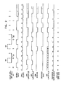
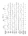
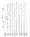
Figures 2-5 are timing diagrams that show the reaction of the circuit for different types of data encoding.
-
Figure 6 shows details of a Code Format Controller (CTRL).
-
The circuit arrangement to be described hereinafter is to be used in a serial communications controller for synchronizing it with bit boundary of an incoming serial data stream. For example, suitable serial communications controller in which the present invention may be used include Z8030/Z8530 serial communications controller (marketed by Zylog, Inc.) SCN26562 (marketed by Signetics Corporation) Intel 82530 (marketed by Intel Corporation) etc. The circuit to be described enables a serial receiver to quickly and continuously synchronize to its transmitters bit cell boundaries for all known serial data encoding methods. The encoded method includes FM0, FM1, Manchester and Differential Manchester. The circuit arrangement also resynchronizes the received data stream if there is a momentary interruption due to noise or low grade cables with a minimal loss of received data due to corruption.
-
Fig. 1 shows a circuit diagram of the invention according to the teachings of the present invention. The circuit diagram includes a clock generator 10 which generates clocking signals on DPLL clock line 12. Preferably, the clock generator 10 is a conventional digital phase lock loop. Since clocking signals that are generated from digital phase lock loop (DPLL) are well known in the technology, a detailed description of a digital phase lock loop for generating clocking signals will not be provided. However, a suitable digital phase lock loop generator is described in the technical manual for the Z8030/Z8530 serial communications controller. Other suitable phase lock loop circuitry is provided in technical reference manuals for serial communications controllers. The clocking signal outputted on DPLL clock 12 is used for clocking serial data into latch L1 13. The output from latch L1 13 is labeled DR and is fed into latch L2 17, logic circuit XOR 14 and logic circuit AOR2 15. Other input signals to logic circuit AOR2 15 are provided by code format controller 16 and logic circuit XNOR 18. It must be noted that circuit AOR2 15 provides first the AND function of the two first inputs, and then the OR function of the resulting signal with the two other inputs. The output from logic circuit AOR2 15 is decoded data which is outputted on the conductor decoded dated 19. Code format controller 16 generates a plurality of controlled status signals on conductors or lines which are labeled NRZ+NRZI, FM1, NRZI+FM0+FM1+DIFF.Man. and NRZ + Manchester. These status or control signals do not change states and their respective values are set depending on the type of encoded data that is being received. In the preferred embodiment of this invention, the line labeled NRZ+NRZI is set to 1 if the serial data that is being received is NRZ or NRZI. The line is a 0 if the serial data is FM0, FM1, Manchester, or Differential Manchester.
-
The line labeled FM1 is set to a 1 if the serial data that is being received is FM1. The line is set to a 0 if the serial data is NRZ, NRZI, FM0, Manchester or Differential Manchester.
-
The line labeled NRZI+FM0+FM1+Diff. Man. is set to a 1 if the serial data is an NRZI, FM0, FM1 or Differential Manchester. It is a 0 if the serial data is NRZ or Manchester.
-
Still referring to Fig. 1, the output of latch L1 13, DR, is clocked into latch L2 17 by the DPLL clock 12. The output (BR) from the positive output signal port Q, of L2 17, is fed into XOR 14. The output from latch L1 13, DR is also fed into XOR 14. The output of XOR 14 on line 24 is fed into logic block AOR1 21 and logic block XNOR 18. The output of AOR1 AR (next) is fed into the data input of synchronization latch L3 23. The negative output of latch L3 is fed into the input of logic block AOR1 21. Note that circuit AOR1 21 provides the AND function of the two first inputs which is then ORed with the third input. The output BR from the positive output of latch L2 17 and DR are fed through logic block XOR 14. The output from XOR 14 is fed into logic blocks AOR1 21 and XNOR 18. The output from AOR1 21, AR (next), is fed into synchronization latch L3 23. The negative output from latch L3 23 is fed back into AOR1 21. The positive output from synchronization latch L3 23 and the DPLL clock are gated by AND gate 20 to provide a clock signal called the coded data clock on decoded data clock line 22. The decoded clock signal and the decoded data signal is fed into latch L4 25. The output of latch L4 25 is the latched data which is provided on conductor labeled latched data (Ltch data). This data is available for use in other parts of the serial communication controller.
-
As stated above, the present circuit is able to handle different types of encoded data. However, the operation of the circuit differs depending on the type of data which is being received. As such, the description of the circuit will be given in terms of the data that is being received.
-
In Figures 2-5, common elements are labelled with like numerals. Figure 2 shows a timing chart when Differential Manchester serial data is received. The bit cells are identified by numeral 20 and the baud cell by numeral 22 (only two of each are marked). Also, "X" in these figures indicates DON'T CARE logic states. Referring again to Figures 1 and 2, the serial data is synchronized by latch L1. This is done to align the serial data to the DPLL clock. The resulting signal is called DR. DR is latched by latch L2 17 to delay DR by one clock cycle. The resulting signal is called BR. Thus, BR(next) is DR. BR(next) denotes the next state of BR. DR is XORed with BR to output a signal on conductor 24 which is ANDed with AR in AOR1 21 to generate the AR(next) input to latch L3 23. The bottom input of AOR1 21 does not affect this function in this case, since it is a zero. The signal (DR XOR BR) on conductor 24 is also inverted through the XNOR 18 since the bottom input is a zero. The signal is passed through AOR2 15 to generate the decoded data signal since the second input on AOR2 15 is a one and the last input is a zero.
-
Latch L3 23 is clocked by the DPLL clock. Its output, AR, is ANDed with the DPLL clock to generate the decoded data clock. Thus, if DR = BR, the serial baud data had not changed, which can occur only at the beginning of bit cell boundaries when DT (transmitted data) is a one. This sets the L3 latch 23 to a zero to resynchronize it. DR = BR indicates the serial data had changed, which occurs at the middle of every bit cell, or at the start of a bit cell whenever DT is a zero. The decoded data clock is used to latch the decoded data to provide the proper data to the downstream logic within the USART (not shown).
-
Figure 3 is the timing chart if frequency modulation 0 (FMO) serial data is received. The circuit, Fig. 1, behaves as follows:
- 1. The serial data is synchronized by latch L1 13. This is done to align the serial data to the DPLL clock. The resultant signal is called DR.
- 2. DR is latched by latch L2 17 to delay DR by one clock cycle. The resultant signal is called BR. Thus, (BR(next) being the next state of L2) is DR.
- 3. DR is XORed with BR. The resultant signal is ANDed with AR in AOR1 21 to generate the AR(next) input to latch L3 23. The bottom input of AOR1 does not affect this function in this case, since it is a zero.
- 4. DR XOR BR is also inverted through the XNOR 18 since the bottom input is a zero. The resultant signal is passed through AOR2 15 to generate the decoded data signal, since the second input on AOR2 15 is a one and the last input is a zero.
- 5. Latch L3 23 is clocked by the DPLL clock. Its output, AR, is ANDed with the DPLL clock to generate the decoded data clock. Thus, if DR = BR, the serial baud data had not changed, which can occur only at the middle of bit cell boundaries when DT is a one. This sets the L3 latch 23 to a zero to resynchronize it. DR = BR indicates the serial data had changed, which occurs at the start of every bit cell or at the middle of a bit cell whenever DT is a zero. The decoded data clock is used to latch the decoded data to provide the proper data to the downstream logic within the USART.
-
Figure 4 is the timing chart for frequency modulation 1 (FM1) serial data. The circuit Figure 1 synchronizes itself to bit cell boundaries each time the transmitted data bit is zero. The circuit of Figure 1 behaves as follows:
- 1. The serial data is synchronized by latch L1 13. This is done to align the serial data to the DPLL clock. The resultant data is called DR.
- 2. DR is latched by latch L2 17 to delay DR by one clock cycle. The resultant data is called BR. Thus, BR(next) is DR.
- 3. DR is XORed with BR. This is ANDed with AR in AOR1 21 to generate the AR(next) input to latch L3 23. The last input of AOR1 21 does not affect this function in this case, since it is a zero.
- 4. DR XOR BR signal on conductor 24 is also passed through the XNOR 18 since the bottom input is a one and is passed through AOR2 15 to generate the decoded data signal since the second input on AOR2 15 is a one and the last input is a zero.
- 5. Latch L3 23 is clocked by the DPLL clock. Its output, AR, is ANDed with the DPLL clock to generate the decoded data clock. Thus, if DR = BR, the serial baud data had not changed, which can occur only at the middle of bit cell boundaries when DT is a zero. This sets the L3 23 latch to a zero to resynchronize it. DR = BR indicates the serial data had changed, which occurs at the start of every bit cell, or at the middle of a bit cell whenever DT is a one. The decoded data clock is used to latch the decoded data to provide the proper data to the downstream logic within the USART.
-
Figure 5 shows a timing chart for Manchester serial data. The circuit synchronizes itself to bit cell boundaries each time a change in the transmitted data bit occurs. The circuit of Figure 1 behaves as follows:
- 1. The serial data is synchronized by latch L1 13. This is done to align the serial data to the DPLL clock and is called DR.
- 2. DR is latched by latch L2 17 to delay DR by one clock cycle. The result is called BR. Thus, BR(next) is DR.
- 3. DR is XORed with BR. The resultant signal on conductor 24 is ANDed with AR in AOR1 21 to generate the AR(next) input to latch L3 23. The bottom input of AOR1 21 does not affect this function in this case, since it is a zero.
- 4. DR is passed through AOR2 15 to generate the decoded data signal, since the second input on AOR2 15 is a zero and the bottom input is a one.
- 5. Latch L3 23 is clocked by the DPLL clock. Its output, AR, is ANDed with the DPLL clock to generate the decoded data clock. Thus, if DR = BR, the serial baud data had not changed, which can occur only at the start of bit cell boundaries when DT changes value. This sets the AR latch to a zero to resynchronize it. DR = BR indicates the serial data had changed, which occurs at the middle of every bit cell, or at the start of a bit cell whenever DT did not change value. The decoded data clock is used to latch the decoded data to provide the proper data to the downstream logic within the USART.
-
For NRZ serial data, the circuit (Figure 1) behaves as follows:
- 1. The serial data is synchronized by latch L1 13. This is done to align the serial data to the DPLL clock and the resultant signal is called DR.
- 2. A one through the bottom input of AOR1 is passed through to latch L3 23 to continuously enable the AND gate so that the DPLL clock and the decoded data clock are equal, which is necessary since the baud and bit rate are equal for NRZ serial data.
- 3. DR is passed through AOR2 15 to generate the decoded data signal since the second input on AOR2 15 is a zero and the bottom input is a one.
-
For NRZI serial data, the circuit (Figure 1) behaves as follows:
- 1. The serial data is synchronized by latch L1 13. This is done to align the serial data to the DPLL clock and the resultant signal is called DR.
- 2. A one through the bottom input of AOR1 is passed through to latch L3 23 to continuously enable the AND gate so that the DPLL clock and the decoded data clock are equal, which is necessary since the baud and bit rate are equal for NRZI serial data.
- 3. DR is XORed with BR in XOR 14 and inverted through the XNOR 18 since the bottom input is a zero and is passed through AOR2 to generate the decoded data signal, since the second input on AOR2 15 is a one and the bottom input is a zero.
-
Figure 6 shows a more detailed circuit diagram for the code format controller 16 of Figure 1. The function of this circuit is to generate and force its outputs to a logical "0" or "1" depending on the encoding format of the received data.
-
Fig. 6 shows a logic circuit diagram for the code format controller. The data format could be decoded of bits B0, B1 and B2, provided from a register or from primary inputs to the chip implementing the alignment function. By way of example, table 1 is a Truth Table setting for the the logical state of the bits for each data format. Thus, for the NRZ format B0, B1 and B2 are all zeros and so forth.
-
The status signals from the circuit diagram would most probably be decodes of 3 bits B0, B1, B2 from a register or from primary inputs to the chip implementing this function. An example of how this decode takes place is shown in Fig. 6.
-
The described self-correcting serial baud/bit alignment circuit improves RAS, shortens error recovery time, eliminates the need for burdensome microcode, and minimal cost in terms of chip real estate.
-
The circuit is in operation continuously. Therefore, correction occurs at all times. The correction sequence does not delay the capture of the received data.
-
The implementation of this circuit eliminates overruns of receiving stations, receiving buffers and the resulting loss of subsequent frames due to a failure to recognize ending delimiters.
-
The circuit does not require stations to start at idle states.
-
While the invention has been particularly shown and described with reference to the preferred embodiments thereof, it will be understood by those skilled in the art that various changes in form and details may be made therein without departing from the spirit and scope of the invention.
-
Having thus described our invention, what we claim as new and desire to secure by Letters Patent is: