EP0339154A2 - carte mémoire - Google Patents
carte mémoire Download PDFInfo
- Publication number
- EP0339154A2 EP0339154A2 EP88308502A EP88308502A EP0339154A2 EP 0339154 A2 EP0339154 A2 EP 0339154A2 EP 88308502 A EP88308502 A EP 88308502A EP 88308502 A EP88308502 A EP 88308502A EP 0339154 A2 EP0339154 A2 EP 0339154A2
- Authority
- EP
- European Patent Office
- Prior art keywords
- patterns
- wiring patterns
- board
- chip
- unit
- Prior art date
- Legal status (The legal status is an assumption and is not a legal conclusion. Google has not performed a legal analysis and makes no representation as to the accuracy of the status listed.)
- Granted
Links
Images


Classifications
-
- H—ELECTRICITY
- H05—ELECTRIC TECHNIQUES NOT OTHERWISE PROVIDED FOR
- H05K—PRINTED CIRCUITS; CASINGS OR CONSTRUCTIONAL DETAILS OF ELECTRIC APPARATUS; MANUFACTURE OF ASSEMBLAGES OF ELECTRICAL COMPONENTS
- H05K1/00—Printed circuits
- H05K1/02—Details
- H05K1/14—Structural association of two or more printed circuits
- H05K1/141—One or more single auxiliary printed circuits mounted on a main printed circuit, e.g. modules, adapters
-
- H—ELECTRICITY
- H01—ELECTRIC ELEMENTS
- H01L—SEMICONDUCTOR DEVICES NOT COVERED BY CLASS H10
- H01L23/00—Details of semiconductor or other solid state devices
- H01L23/52—Arrangements for conducting electric current within the device in operation from one component to another, i.e. interconnections, e.g. wires, lead frames
- H01L23/538—Arrangements for conducting electric current within the device in operation from one component to another, i.e. interconnections, e.g. wires, lead frames the interconnection structure between a plurality of semiconductor chips being formed on, or in, insulating substrates
- H01L23/5385—Assembly of a plurality of insulating substrates
-
- H—ELECTRICITY
- H01—ELECTRIC ELEMENTS
- H01L—SEMICONDUCTOR DEVICES NOT COVERED BY CLASS H10
- H01L23/00—Details of semiconductor or other solid state devices
- H01L23/52—Arrangements for conducting electric current within the device in operation from one component to another, i.e. interconnections, e.g. wires, lead frames
- H01L23/538—Arrangements for conducting electric current within the device in operation from one component to another, i.e. interconnections, e.g. wires, lead frames the interconnection structure between a plurality of semiconductor chips being formed on, or in, insulating substrates
- H01L23/5386—Geometry or layout of the interconnection structure
-
- H—ELECTRICITY
- H01—ELECTRIC ELEMENTS
- H01L—SEMICONDUCTOR DEVICES NOT COVERED BY CLASS H10
- H01L2224/00—Indexing scheme for arrangements for connecting or disconnecting semiconductor or solid-state bodies and methods related thereto as covered by H01L24/00
- H01L2224/01—Means for bonding being attached to, or being formed on, the surface to be connected, e.g. chip-to-package, die-attach, "first-level" interconnects; Manufacturing methods related thereto
- H01L2224/42—Wire connectors; Manufacturing methods related thereto
- H01L2224/47—Structure, shape, material or disposition of the wire connectors after the connecting process
- H01L2224/48—Structure, shape, material or disposition of the wire connectors after the connecting process of an individual wire connector
- H01L2224/4805—Shape
- H01L2224/4809—Loop shape
- H01L2224/48091—Arched
-
- H—ELECTRICITY
- H01—ELECTRIC ELEMENTS
- H01L—SEMICONDUCTOR DEVICES NOT COVERED BY CLASS H10
- H01L2224/00—Indexing scheme for arrangements for connecting or disconnecting semiconductor or solid-state bodies and methods related thereto as covered by H01L24/00
- H01L2224/01—Means for bonding being attached to, or being formed on, the surface to be connected, e.g. chip-to-package, die-attach, "first-level" interconnects; Manufacturing methods related thereto
- H01L2224/42—Wire connectors; Manufacturing methods related thereto
- H01L2224/47—Structure, shape, material or disposition of the wire connectors after the connecting process
- H01L2224/48—Structure, shape, material or disposition of the wire connectors after the connecting process of an individual wire connector
- H01L2224/481—Disposition
- H01L2224/48151—Connecting between a semiconductor or solid-state body and an item not being a semiconductor or solid-state body, e.g. chip-to-substrate, chip-to-passive
- H01L2224/48221—Connecting between a semiconductor or solid-state body and an item not being a semiconductor or solid-state body, e.g. chip-to-substrate, chip-to-passive the body and the item being stacked
- H01L2224/48225—Connecting between a semiconductor or solid-state body and an item not being a semiconductor or solid-state body, e.g. chip-to-substrate, chip-to-passive the body and the item being stacked the item being non-metallic, e.g. insulating substrate with or without metallisation
- H01L2224/48227—Connecting between a semiconductor or solid-state body and an item not being a semiconductor or solid-state body, e.g. chip-to-substrate, chip-to-passive the body and the item being stacked the item being non-metallic, e.g. insulating substrate with or without metallisation connecting the wire to a bond pad of the item
-
- H—ELECTRICITY
- H05—ELECTRIC TECHNIQUES NOT OTHERWISE PROVIDED FOR
- H05K—PRINTED CIRCUITS; CASINGS OR CONSTRUCTIONAL DETAILS OF ELECTRIC APPARATUS; MANUFACTURE OF ASSEMBLAGES OF ELECTRICAL COMPONENTS
- H05K2201/00—Indexing scheme relating to printed circuits covered by H05K1/00
- H05K2201/10—Details of components or other objects attached to or integrated in a printed circuit board
- H05K2201/10613—Details of electrical connections of non-printed components, e.g. special leads
- H05K2201/10621—Components characterised by their electrical contacts
- H05K2201/10689—Leaded Integrated Circuit [IC] package, e.g. dual-in-line [DIL]
-
- H—ELECTRICITY
- H05—ELECTRIC TECHNIQUES NOT OTHERWISE PROVIDED FOR
- H05K—PRINTED CIRCUITS; CASINGS OR CONSTRUCTIONAL DETAILS OF ELECTRIC APPARATUS; MANUFACTURE OF ASSEMBLAGES OF ELECTRICAL COMPONENTS
- H05K2203/00—Indexing scheme relating to apparatus or processes for manufacturing printed circuits covered by H05K3/00
- H05K2203/15—Position of the PCB during processing
- H05K2203/1572—Processing both sides of a PCB by the same process; Providing a similar arrangement of components on both sides; Making interlayer connections from two sides
-
- H—ELECTRICITY
- H05—ELECTRIC TECHNIQUES NOT OTHERWISE PROVIDED FOR
- H05K—PRINTED CIRCUITS; CASINGS OR CONSTRUCTIONAL DETAILS OF ELECTRIC APPARATUS; MANUFACTURE OF ASSEMBLAGES OF ELECTRICAL COMPONENTS
- H05K3/00—Apparatus or processes for manufacturing printed circuits
- H05K3/30—Assembling printed circuits with electric components, e.g. with resistor
- H05K3/32—Assembling printed circuits with electric components, e.g. with resistor electrically connecting electric components or wires to printed circuits
- H05K3/34—Assembling printed circuits with electric components, e.g. with resistor electrically connecting electric components or wires to printed circuits by soldering
- H05K3/341—Surface mounted components
- H05K3/3431—Leadless components
- H05K3/3442—Leadless components having edge contacts, e.g. leadless chip capacitors, chip carriers
-
- H—ELECTRICITY
- H05—ELECTRIC TECHNIQUES NOT OTHERWISE PROVIDED FOR
- H05K—PRINTED CIRCUITS; CASINGS OR CONSTRUCTIONAL DETAILS OF ELECTRIC APPARATUS; MANUFACTURE OF ASSEMBLAGES OF ELECTRICAL COMPONENTS
- H05K3/00—Apparatus or processes for manufacturing printed circuits
- H05K3/36—Assembling printed circuits with other printed circuits
- H05K3/368—Assembling printed circuits with other printed circuits parallel to each other
Definitions
- This invention relates to an IC package having a plurality of multiterminal IC chips, such as a memory card.
- the above IC chips for semiconductor memories have each thirty to fifty connecting terminals, and these connecting terminals are common connecting terminals such as data bus terminals and control bus terminals, with the exception of some individual terminals such as a chip enable terminal.
- these connecting terminals are common connecting terminals such as data bus terminals and control bus terminals, with the exception of some individual terminals such as a chip enable terminal.
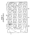
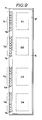
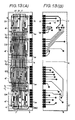
- FIG. 1 is a plan view of a conventional memory card
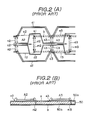
- FIG. 2(A) is a partially plan view illustrating connecting and wiring between IC chips of the conventional memory card
- FIG. 2(B) is a partially sectional view thereof.
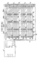
- a substrate 50 which forms a memory card 5 is a double-sided wiring board, as shown in FIG. 2(B).
- On an upper surface 50a twenty IC chips denoted at A1 to A20 are bonded, and upper surface patterns "a” each shown by a solid line, bonding patterns "n” each shown by a solid circle and through-hole patterns "m” each shown by an open circle are provided.
- lower surface patterns "b” each shown by a dashed line are provided and connected to upper surface 50a by means of through-hole patterns "m”.
- each IC chip “A” is square-shaped and one pair of opposite edges "c” and “d” are each provided with twenty connecting terminals, while the other pair of opposite edges “e” and “f” are not provided with any connecting terminal. And all the connecting terminals provided along edge “c” are common connecting terminals, and among the connecting terminals provided along edge "d", nineteen terminals are common connecting terminals and one terminal is a chip enable terminal.
- connecting terminals provided along edge c2 of IC chip A2 are connected to respective bonding patterns n2, and twenty connecting terminals provided along edge d2 are connected to respective through-hole patterns m2 each by wire bonding.
- connecting terminals along edge c3 are connected to respective bonding patterns n3
- connecting terminals along edge d3 are connected to respective through-hole patterns m3 each by wire bonding.
- Half (ten in number) of bonding patterns n2 connected to connecting terminals of IC chip A2 are connected to respective bonding patterns n3 connected to the common connecting terminals of IC chip A3, by means of ten upper surface patterns a1 which are arranged on the upper part of IC chip A2 so as to avoid through-hole patterns m2, and the remaining bonding patterns n2 are connected to the corresponding bonding patterns of IC chip A3 by means of ten upper surface patterns a2 which are arranged on the lower part of IC chip A2.
- Furthermore through-hole patterns m2 connected to connecting terminals of IC chip A2 are directly connected to through-hole patterns m3 of IC chip A3 by means of lower surface patterns "b" arranged on the lower surface of substrate 50.
- the above-mentioned structure allows connections between common connecting terminals which are provided along one edge of each IC chip to be made on upper surface 50a to which IC chips are bonded.
- connection structure between the respective IC chips. Next, the entire connection structure will be described with reference to FIG. 1.
- IC chips A1 to A20 are arranged and bonded in four rows in the arrangement direction of IC chips on substrate 50, as shown by arrow B.
- the IC chips can be connected on the same plane without crossing the connections between IC chips throughout each of rows.
- the conventional memory card is designed so that many IC chips are directly packaged on a single circuit board. Therefore, wiring between common connecting terminals must be divided into the upper surface and the lower surface of the substrate. As a result, since the circuit board needs a lot of through-hole patterns and high-density wiring patterns, there are problems of increased costs caused by a costly process for making through-hole patterns and of decreased yields caused by high-density packaging of IC chips onto high-density wiring patterns.
- the object of the present invention is to provide an IC package which is free of the above problems, low in cost and has a high packaging density.
- An IC package comprising: (a) a main board including a plurality of external connecting terminal patterns aligned along one of the edges of the board, and a plurality of wiring patterns running in a row direction of the board on at least a front side of the board, the external connecting terminal patterns and the wiring patterns being connected by means of wiring patterns without crossing each other on the front side of the board; and (b) a plurality of IC chip units each having a single auxiliary board and a plurality of IC chips mounted on a front side of the single auxiliary board, the auxiliary board being rectangular and including a plurality of unit-connecting terminal patterns aligned along one of the longitudinal edges of the auxiliary board, the auxilairy board unit-connecting terminal patterns corresponding to the plurality of main board row-direction wiring patterns, the auxiliary board further including plural columns of wiring patterns running in a column direction of the auxiliary board, and the plurality of IC chips being mounted on the plural columns of wiring patterns
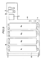
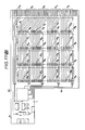
- FIG. 3 is a plan view of a memory card of a first embodiment of the present invention
- a circuit board 1 which forms a memory card 10 is provided with a cutout portion 1a for holding a power supply device; a memory package portion 1b; and a decoder (chip selecting circuit) package portion 1c.
- a plurality of external connecting terminals T are provided.
- chip units B1, B2, B3 and B4 as will be discussed later are aligned, and a plurality of chip components are arranged around the chip units. Also on the decoder package portion 1c, elements such as a decoder IC 2 and a capacitor 3 are packaged.
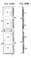
- FIGS. 4(A) and 4(B) are a plan view and a sectional view of the chip unit B1 shown in FIG. 3.
- the chip unit B1 has four memory IC chips D1 to D4 packaged as one group on an auxiliary board 4 and encapsulated with an encapsulating resin 6.
- a plurality of unit-connecting terminals t are provided and they are divided into four blocks t1 to t4.
- the respective connecting terminals of the four IC chips D1 to D4 are connected in common by means of common connecting patterns on the auxiliary board 4.
- each block is provided with a chip enable connecting terminal te (CE connecting terminal) for connecting each of chip enable terminals of IC chips D1 to D4.
- CE connecting terminal CE connecting terminal
- the number of the unit-connecting terminals t of the chip unit B1 reaches a total of thirty-two (the twenty-eight common connecting terminals and four chip enable terminals, each enable terminal being provided in each of IC chips D1 to D4). These thirty-two terminals are divided into the respective blocks t1 to t4, each eight.
- chip units B2, B3 and B4 shown in FIG. 3 are of the same construction as chip unit B1 including the number and arrangement of unit-connecting terminals.
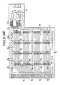
- FIGS. 5(A) and 5(B) are a front view and a back view of the circuit board 1 shown in FIG. 3 and show wiring patterns respectively.
- the memory package portion 1b on the front of the circuit board 1 is formed with bonding patterns P1, P2, P3, P4 and P d corresponding to the positions of the respective unit-connecting terminals t1, t2, t3, t4 and t e when chip units B1, B2, B3 and B4 shown in FIG.
- the decoder IC (chip selecting circuit) 2 is packaged by means of bonding patterns Ps.
- the unit-connecting terminals t1, t2, t3 and t4 of the chip unit B1 which is mounted on the position shown by the dot and dash line are located on the bonding patterns P1, P2, P3 and P4 on the circuit board 1. By soldering the terminals in this state, the packaged state shown in FIG. 3 is established.
- each CE connecting terminal t e provided in each block of unit-connecting terminals of chip unit B1 is soldered and connected via a through-hole pattern to the back of the circuit board 1.
- the respective bonding patterns P1, P2, P3 and P4 except CE bonding patterns P d are connected to the respective blocks of T1, T2, T3 and T4 of the corresponding external connecting terminals.
- the back of the circuit board 1 is provided with through-hole patterns P d ′ connected to the front CE bonding patterns P d .
- All the CE connecting terminals t e are connected via throughhole patterns Pd′ to the decoder IC (chip selecting circuit) 2 by means of the wiring patterns.
- the decoder IC 2 is supplied with the decoder (chip selecting circuit) control signals via external connecting terminals T0 for enable control of IC chips packaged on each of the chip units.
- the chip unit structure in which a plurality of IC chips are compactly packaged allows the wiring density on the circuit board 1 to be decreased, and the number of through-hole patterns and the number of soldering terminals are remarkably decreased.
- the number of soldering operations of the present invention is less than 1/3 of that of the conventional example.
- the number of wires and the number of through-hole patterns can be considerably decreased, and a large space between wiring patterns can be provided.
- FIGS. 6 and 7 show a memory card according to the second embodiment of the invention, in which FIG. 6(A) is a plan view thereof and FIG. 6(B) is a sectional view taken along the line VIB-VIB of FIG. 6(A).
- the memory package portion 1b on the front side of the circuit board 1 is provided with the chip units B1, B2, B3 and B4 identical with those discussed with reference to FIGS. 4(A) and 4(B) (first embodiment), and the memory package portion 1b′ on the back side of the circuit board 1 is provided with chip units B5, B6 and B7.
- FIGS. 7(A) and 7(B) are a front view and a back view of the circuit board 1 shown in FIG. 6(A) and show wiring patterns respectively.
- the memory package portion 1b on the front of the circuit board 1 is formed with bonding patterns P1, P2, P3, P4 and P e corresponding to the positions of the respective unit-connecting terminals t1, t2, t3, t4 and t e when chip units B1, B2, B3, and B4 are aligned as shown in FIG.
- the decoder IC chip selecting circuit
- the respective chip enable bonding patterns P e CE bonding patterns of the bonding patterns P1, P2, P3, P4 and P e are connected.
- bonding patterns P1, P2, P3, P4 and P e are formed corresponding to the positions of the respective unit-connecting terminals t1, t2, t3, t4 and t e when chip units B5, B6 and B7 are aligned as shown by dot and dash lines, and like the front memory package portion 1b, common bonding patterns P1, P2, P3 and P4 for each chip unit B5, B6 and B7 and the external connecting terminals T1, T2, T3 and T4 corresponding to these bonding patterns P1, P2, P3 and P4 are connected in common by means of wiring patterns.
- the packaging and connecting/wiring on the memory package portions 1b and 1b′ will be explained, taking, as an example, the chip units B1 and B5.
- the unit-connecting terminals t1, t2, t3 and t4 (FIG. 4(A)) of the chip unit B1 which is mounted on the position shown by the dot and dash line, with the unit-connecting terminals placed in the direction of arrow, are located on the bonding patterns P1, P2, P3 and P4 on the circuit board 1.
- the packaged state shown in FIG. 6(A) is established.
- the respective bonding patterns P1, P2, P3 and P4 except CE bonding patterns P e are, as mentioned above, connected to the respective blocks of T1, T2, T3, and T4 of the corresponding external connecting terminals.
- chip units B5 to B7 identical with the front chip units B1 to B4 are mounted, with the connecting terminals placed in the direction opposite to the direction shown by the arrows for the chip units B1 to B4.
- the respective unit-connecting terminals t1, t2, t3 and t4 of chip unit B5 are located on the bonding patterns P1, P2, P3 and P4 on the circuit board 1.
- FIGS. 8 to 10 show a memory card according to the third embodiment of the invention, in which FIG. 8(A) is a plan view thereof and FIG. 8(B) is a sectional view taken along the line VIIIB-VIIIB of FIG. 8(A).
- the memory package portion 1b on the front of the circuit board is provided with the first chip units (those shown in FIGS. 4(A) and 4(B)) identical with the chip units of the first and the second embodiments.
- the second chip units B101, B102, B103 and B104 different from the chip units in the above embodiments are aligned, as will be discussed later.
- the plan view of the circuit board 1 shown in FIG. 10(A) is identical with the plan view of the circuit board 1 according to the second embodiment (FIG. 7(A)).
- the memory package portion 1b on the front of the circuit board 1 is formed with bonding patterns P1, P2, P3, P4 and P e corresponding to the positions of the respective unit connecting terminals t1, t2, t3, t4 and t e when chip units B1, B2, B3 and B4 shown in FIG. 4(A) are aligned as shown by dot and dash lines, and common bonding patterns P1, P2, P3 and P4 for each chip unit and external connecting terminals T1, T2, T3 and T4 corresponding to bonding patterns P1, P2, P3 and P4 are connected in common by means of wiring patterns.
- the decoder IC 2 is packaged and to this decoder IC 2, the respective chip enable bonding patterns P e (CE bonding patterns) of the bonding patterns P1, P2, P3, P4 and P e are connected.
- FIG. 9 is a plan view of a second chip unit B′ which forms each chip unit B101, B102, B103 and B104 shown in FIG. 8(B).
- the second chip unit B′ is the same as the first unit B shown in FIG. 4(A) in the basic construction but different in the arrangement of connecting terminals.
- the other edge in the longitudinal direction of the auxiliary board (the edge opposite to the first chip unit B (B1, B2, B3 and B4)) has a plurality of unit connecting terminals divided into four blocks t1 to t4.
- FIG. 10(B) is a back view of the circuit board 1 and shows the respective wiring patterns.
- bonding patterns P1, P2, P3 and P4 are formed corresponding to the positions of the respective unit connecting terminals t1, t2, t3, t4 and t e when chip units B101, B102, B103 and B104 are aligned as shown by dot and dash lines, and like the front memory package portion 1b, common bonding patterns P1, P2, P3 and P4 of each chip unit and the external connecting terminals T1, T2, T3 and T4 corresponding to these bonding patterns are connected in common by means of wiring patterns.
- the bonding patterns P1, P2, P3, P4 and P e and external connecting terminals T1, T2, T3 and T4 are provided in corresponding positions on two sides of the circuit board.
- each CE bonding pattern P e is connected to back patterns of the decoder IC 2, and part of the back patterns are in turn connected to external connecting terminals T0.
- the aforementioned chip units B1 to B4 are mounted on the positions each shown by a dot and dash line, with the chip units B1, B2, B3 and B4 placed in the direction of arrows.
- the unit-connecting terminals t1, t2, t3 and t4 of each chip unit B1 to B4 are located on the bonding patterns P1, P2, P3 and P4 on the circuit board 1.
- each CE connecting terminal t e provided in each block of unit-connecting terminals of chip units B1 to B4 is soldered.
- the respective bonding patterns P1, P2, P3 and P4 except CE bonding patterns P e are, as mentioned above, connected to the respective blocks of T1, T2, T3 and T4 of the corresponding external connecting terminals.
- the common unit-connecting terminals of each chip unit are linearly connected by means of the wiring patterns, and by conforming bonding patterns P1, P2, P3 and P4 to external connecting terminals T1, T2, T3 and T4 in arrangement and procedure, plane connections can be made without crossing connections.
- FIG. 10(B) on the positions shown by dot and dash lines, the second chip units B101 to B104 are mounted, with the connecting terminals placed in the direction shown by the arrows.
- the respective unit-connecting terminals t1, t2, t3 and t4 of chip units B101 to B104 are located on the bonding patterns P1, P2, P3 and P4.
- the respective CE connecting terminals te provided in the respective blocks of unit-connecting terminals of chip units B101 to B104 are soldered.
- the respective bonding patterns P1, P2, P3 and P4 except CE bonding patterns P e are, as mentioned above, connected to the corresponding external connecting terminals T1, T2, T3 and T4.
- CE connecting terminals t e are connected via EC bonding patterns P e to the decoder IC 2 by means of the wiring patterns. Then, the decoder IC 2 is supplied with the decoder control signals via external connecting terminals T0 for enable control of IC chip packaged on each of the chip units.
- the same wiring patterns are formed, and the corresponding patterns are connected by means of a series of through-hole patterns.
- two types of chip units whose unit-connecting terminals are reversed in direction are packaged on both sides of the circuit board 1. As a result, the packaging density is remarkably enhanced.
- FIGS. 11(A) and 11(B) illustrate a fourth embodiment of the present invention, in which FIG. 11(A) is a plan view of the circuit board and FIG. 11(B) is a back view thereof.
- Connections between the external connecting patterns T0 on the board and the input terminals of the decoder IC (chip selecting circuit) 2 and connections between the output terminals of the decoder and the chip enable terminals P e on the board are made by means of the wiring patterns on the board.
- connections between the board and the components to be mounted on the board can be made only on the front (one side) of the board.
- FIG. 11(B) shows its back side.
- connections between the board and the components to be mounted on the board can be made only on the back side (one side).
- the back wiring patterns correspond to the front wiring patterns so as to make the arrangement similar to that of the third embodiment.
- both the front and back sides are independent, they can be made into different types from each other.
- FIGS. 12(A) and 12(B) are a plan view and a sectional view illustrating another embodiment of the chip unit B according to the present invention.
- This embodiment is different from the embodiment of FIG. 4 in that the encapsulating resin 6 is divided into an encapsulating resin block 6a for encapsulating IC chips D1 and D2 and an encapsulating resin block 6b for encapsulating IC chips D3 and D4 so as to be divided into a first block Ba and a second block Bb, with a center line K shown by a dashed line being a border, and in that a plurality of common connecting patterns L are exposed between the encapsulating resing blocks 6a and 6b of the auxiliary board 4.
- the purpose of the aforementioend embodiment is to further improve the total yield by chip unit structure.
- the reliability of chip unit B is checked with reference to the first block Ba and the second block Bb. Should any one be found to be defective, the chip unit B is cut to separate along the center line K, and instead of the defective block, a good block is joined along the center line K and at the same time, common connecting patterns L are connected by a method such as soldering so as to complete a reproduced chip unit B.
- the four IC chips packaged on the chip unit are discarded, but in the present embodiment, only two IC chips are discarded and the remaining two IC chips are saved.
- the total yield can be improved.
- the number of the IC chips packaged within the chip unit and the number of the chip units packaged on the circuit board can be selected at will.
- FIG. 13(A) is a plan view of the auxiliary board for the chip unit shown in FIG. 12(A) (mold and IC chips are removed), and FIG. 13(B) is its back view.
- the auxiliary board 4 is rectangular, has unit-connecting terminal patterns along one edge of the longitudinal edges (right side in this embodiment) and the plural columns of wiring patterns which are in parallel with the aligned unit-connecting terminals.
- Each of the plural columns of wiring patterns, for example, b is bonded to each of the corresponding terminals a1, a2, a3 and a4 of IC chips D1, D2, D3 and D4 mounted on the auxiliary board at the corresponding positions (bonding portions) b1, b2, b3 and b4. These bonding portions are made wider than the other portions for facilitating bonding operations.
- the back side is coated with an insulating coating 4′ except the unit-connecting terminal patterns.
- the wiring pattern b is provided with a through-hole pattern c leading to the back side. This through-hole pattern is connected to the back wiring pattern d and connected to the unit-connecting terminal pattern A by means of the back wiring pattern d.
- a GND terminal is connected from a unit-connecting terminal pattern GND to the column-direction wiring pattern g by means of a separately provided front wiring pattern f.
- the surface of the auxiliary board 4 is coated with the insulating coating 4′ except for the regions of the bonding portions of the front wiring patterns and the middle portion K.
- IC chips D1, D2, D3 and D4 are mounted and then molded with resin 6. Thus IC chips shown in FIG. 12 are completed.
- the present invention has a great effect on the improvement in the marketability of IC packages.
Landscapes
- Physics & Mathematics (AREA)
- Engineering & Computer Science (AREA)
- Microelectronics & Electronic Packaging (AREA)
- Condensed Matter Physics & Semiconductors (AREA)
- General Physics & Mathematics (AREA)
- Computer Hardware Design (AREA)
- Power Engineering (AREA)
- Geometry (AREA)
- Credit Cards Or The Like (AREA)
- Structures For Mounting Electric Components On Printed Circuit Boards (AREA)
Applications Claiming Priority (6)
| Application Number | Priority Date | Filing Date | Title |
|---|---|---|---|
| JP102998/88 | 1988-04-26 | ||
| JP63102998A JP2664720B2 (ja) | 1988-04-26 | 1988-04-26 | Ic実装装置 |
| JP118169/88 | 1988-05-17 | ||
| JP63118169A JP2608915B2 (ja) | 1988-05-17 | 1988-05-17 | Ic実装装置 |
| JP136856/88 | 1988-06-03 | ||
| JP63136856A JPH01305554A (ja) | 1988-06-03 | 1988-06-03 | Ic実装装置 |
Publications (3)
| Publication Number | Publication Date |
|---|---|
| EP0339154A2 true EP0339154A2 (fr) | 1989-11-02 |
| EP0339154A3 EP0339154A3 (en) | 1990-09-12 |
| EP0339154B1 EP0339154B1 (fr) | 1994-11-17 |
Family
ID=27309860
Family Applications (1)
| Application Number | Title | Priority Date | Filing Date |
|---|---|---|---|
| EP88308502A Expired - Lifetime EP0339154B1 (fr) | 1988-04-26 | 1988-09-14 | carte mémoire |
Country Status (3)
| Country | Link |
|---|---|
| US (1) | US4942453A (fr) |
| EP (1) | EP0339154B1 (fr) |
| DE (1) | DE3852131T2 (fr) |
Cited By (6)
| Publication number | Priority date | Publication date | Assignee | Title |
|---|---|---|---|---|
| GB2237691A (en) * | 1989-10-30 | 1991-05-08 | Mitsubishi Electric Corp | Semiconductor device and wiring board module |
| EP0680082A1 (fr) * | 1993-11-12 | 1995-11-02 | Seiko Epson Corporation | Structure et procede de montage de dispositif a semi-conducteurs et dispositif d'affichage a cristaux liquides |
| US5490041A (en) * | 1993-11-15 | 1996-02-06 | Matsushita Electric Industrial Co., Ltd. | Semiconductor integrated circuit module and a semiconductor integrated circuit device stacking the same |
| FR2727223A1 (fr) * | 1994-11-23 | 1996-05-24 | Fast France Adv Sys Tech Sarl | Terminal securise multifonction de saisie et de traitement, utilisable notamment dans le domaine bancaire, dans le domaine des jeux et dans le domaine de la gestion electronique de documents |
| EP0720232A1 (fr) * | 1993-09-14 | 1996-07-03 | Kabushiki Kaisha Toshiba | Circuit multipuce |
| EP0786809A1 (fr) * | 1991-02-28 | 1997-07-30 | Hitachi, Ltd. | Empaquetage pour circuit électronique |
Families Citing this family (13)
| Publication number | Priority date | Publication date | Assignee | Title |
|---|---|---|---|---|
| US5663901A (en) * | 1991-04-11 | 1997-09-02 | Sandisk Corporation | Computer memory cards using flash EEPROM integrated circuit chips and memory-controller systems |
| JP3484705B2 (ja) * | 1991-07-18 | 2004-01-06 | ソニー株式会社 | 半導体ウエハ |
| JP3123616B2 (ja) * | 1991-10-09 | 2001-01-15 | キヤノン株式会社 | 液晶表示装置の実装方法 |
| US5243497A (en) * | 1992-09-29 | 1993-09-07 | Texas Instruments | Chip on board assembly |
| US5754399A (en) * | 1992-09-30 | 1998-05-19 | International Business Machines Corporation | Direct coupled CPU package |
| JP3396541B2 (ja) * | 1993-08-30 | 2003-04-14 | 株式会社東芝 | 混成集積回路装置を搭載した回路基板 |
| US5691569A (en) * | 1995-12-20 | 1997-11-25 | Intel Corporation | Integrated circuit package that has a plurality of staggered pins |
| JP2005123362A (ja) * | 2003-10-16 | 2005-05-12 | Hitachi Ltd | 接続用取付基板及びディスクアレイ制御装置の接続用取付基板 |
| JP2007059693A (ja) * | 2005-08-25 | 2007-03-08 | Toshiba Corp | 半導体メモリカードおよび半導体メモリカードの製造方法 |
| US7935899B2 (en) * | 2005-08-31 | 2011-05-03 | Sanyo Electric Co., Ltd. | Circuit device and method of manufacturing the same |
| JP2009182104A (ja) * | 2008-01-30 | 2009-08-13 | Toshiba Corp | 半導体パッケージ |
| JP5193837B2 (ja) * | 2008-03-21 | 2013-05-08 | 株式会社東芝 | 半導体メモリカード |
| US8472199B2 (en) * | 2008-11-13 | 2013-06-25 | Mosaid Technologies Incorporated | System including a plurality of encapsulated semiconductor chips |
Citations (2)
| Publication number | Priority date | Publication date | Assignee | Title |
|---|---|---|---|---|
| WO1980001220A1 (fr) * | 1978-11-29 | 1980-06-12 | Hughes Aircraft Co | Dispositif microelectronique a structure tridimensionnelle |
| FR2513477A1 (fr) * | 1980-09-29 | 1983-03-25 | Asea Ab | Equipement electrique du type comprenant plusieurs cartes de circuit imprime raccordees a un plan de connexions |
Family Cites Families (8)
| Publication number | Priority date | Publication date | Assignee | Title |
|---|---|---|---|---|
| US3300686A (en) * | 1963-07-30 | 1967-01-24 | Ibm | Compatible packaging of miniaturized circuit modules |
| US3260982A (en) * | 1963-12-31 | 1966-07-12 | Ibm | Flat cable strain relief |
| JPS57181161A (en) * | 1981-04-30 | 1982-11-08 | Sanyo Electric Co Ltd | Transistor |
| JPS5830176A (ja) * | 1981-08-14 | 1983-02-22 | Nippon Telegr & Teleph Corp <Ntt> | 超伝導素子実装用部品の製作方法 |
| US4439809A (en) * | 1982-02-22 | 1984-03-27 | Sperry Corporation | Electrostatic discharge protection system |
| JPS6099566U (ja) * | 1983-12-10 | 1985-07-06 | アルプス電気株式会社 | プリント基板端子部の接続構造 |
| US4704599A (en) * | 1984-06-20 | 1987-11-03 | Kimmel Arthur T | Auxiliary power connector and communication channel control circuit |
| US4780792A (en) * | 1986-08-15 | 1988-10-25 | Honeywell Inc. | Sliding circuit card ejection apparatus and method |
-
1988
- 1988-09-14 DE DE3852131T patent/DE3852131T2/de not_active Expired - Fee Related
- 1988-09-14 EP EP88308502A patent/EP0339154B1/fr not_active Expired - Lifetime
- 1988-09-15 US US07/244,794 patent/US4942453A/en not_active Expired - Fee Related
Patent Citations (2)
| Publication number | Priority date | Publication date | Assignee | Title |
|---|---|---|---|---|
| WO1980001220A1 (fr) * | 1978-11-29 | 1980-06-12 | Hughes Aircraft Co | Dispositif microelectronique a structure tridimensionnelle |
| FR2513477A1 (fr) * | 1980-09-29 | 1983-03-25 | Asea Ab | Equipement electrique du type comprenant plusieurs cartes de circuit imprime raccordees a un plan de connexions |
Non-Patent Citations (1)
| Title |
|---|
| INTERNATIONAL ELECTRON DEVICES 6 September 1987, WASHINGTON, pages 104 - 106; MALHI ET AL.: "ORTHOGONAL CHIP MOUNT- A 3D HYBRID WAFER SCALE INTEGRATION TECHNOLOGY" * |
Cited By (11)
| Publication number | Priority date | Publication date | Assignee | Title |
|---|---|---|---|---|
| GB2237691A (en) * | 1989-10-30 | 1991-05-08 | Mitsubishi Electric Corp | Semiconductor device and wiring board module |
| GB2237691B (en) * | 1989-10-30 | 1993-08-25 | Mitsubishi Electric Corp | Electronic device |
| EP0786809A1 (fr) * | 1991-02-28 | 1997-07-30 | Hitachi, Ltd. | Empaquetage pour circuit électronique |
| EP0720232A1 (fr) * | 1993-09-14 | 1996-07-03 | Kabushiki Kaisha Toshiba | Circuit multipuce |
| EP0720232A4 (fr) * | 1993-09-14 | 1996-11-13 | Toshiba Kk | Circuit multipuce |
| EP0680082A1 (fr) * | 1993-11-12 | 1995-11-02 | Seiko Epson Corporation | Structure et procede de montage de dispositif a semi-conducteurs et dispositif d'affichage a cristaux liquides |
| EP0680082A4 (fr) * | 1993-11-12 | 1997-04-02 | Seiko Epson Corp | Structure et procede de montage de dispositif a semi-conducteurs et dispositif d'affichage a cristaux liquides. |
| US5490041A (en) * | 1993-11-15 | 1996-02-06 | Matsushita Electric Industrial Co., Ltd. | Semiconductor integrated circuit module and a semiconductor integrated circuit device stacking the same |
| FR2727223A1 (fr) * | 1994-11-23 | 1996-05-24 | Fast France Adv Sys Tech Sarl | Terminal securise multifonction de saisie et de traitement, utilisable notamment dans le domaine bancaire, dans le domaine des jeux et dans le domaine de la gestion electronique de documents |
| EP0714075A1 (fr) * | 1994-11-23 | 1996-05-29 | F.A.S.T. -France Advanced Systems Technology S.A.R.L. | Terminal sécurisé multifonction de saisie et de traitement, utilisable notamment dans les domaines bancaire, de jeux et de la gestion électronique de documents |
| US6011850A (en) * | 1994-11-23 | 2000-01-04 | Jean-Marie Gatto | Securized, multifunction, acquisition and processing terminal usable in the banking sector, in connection with games and in the electronic management of documents |
Also Published As
| Publication number | Publication date |
|---|---|
| DE3852131T2 (de) | 1995-05-18 |
| EP0339154B1 (fr) | 1994-11-17 |
| EP0339154A3 (en) | 1990-09-12 |
| DE3852131D1 (de) | 1994-12-22 |
| US4942453A (en) | 1990-07-17 |
Similar Documents
| Publication | Publication Date | Title |
|---|---|---|
| EP0339154A2 (fr) | carte mémoire | |
| US5313096A (en) | IC chip package having chip attached to and wire bonded within an overlying substrate | |
| US6788560B2 (en) | Semiconductor device and process for manufacturing the same | |
| EP0430458A2 (fr) | Empaquetages pour puces semi-conductrices | |
| US5789816A (en) | Multiple-chip integrated circuit package including a dummy chip | |
| EP0595021A1 (fr) | Empaquetage à cadre de conducteurs perfectionné pour dispositifs électroniques | |
| EP0408779B1 (fr) | Module semi-conducteur de mémoire à haute densité | |
| WO1996032745A1 (fr) | Empilage de puces et procede de fabrication correspondant | |
| EP0294015B1 (fr) | Dispositif ayant une platine pour connexion de plusieurs puces de circuits intégrés | |
| US4710680A (en) | Driver device mounting for a flat matrix display panel | |
| KR20020020225A (ko) | 스택된 모듈을 포함한 전자 부품 및 그의 제조 방법 | |
| US5640308A (en) | Field programmable circuit module | |
| EP1118121B1 (fr) | Montage de dispositif a semiconducteur configure par codage de plages de connexion adjacentes | |
| US6222211B1 (en) | Memory package method and apparatus | |
| JPH01144664A (ja) | 半導体メモリ用集積回路装置 | |
| EP0352805A2 (fr) | Ligne à retard à constantes distribuées et son procédé de fabrication | |
| US6084303A (en) | Integrated circuit comprising connection pads emerging on one surface | |
| US7274109B2 (en) | Modular bonding pad structure and method | |
| JP2664720B2 (ja) | Ic実装装置 | |
| JPS6356950A (ja) | 複合化集積回路装置 | |
| US6225821B1 (en) | Package migration for related programmable logic devices | |
| JPS58184735A (ja) | 集積回路チツプ | |
| JPH04355192A (ja) | Icカード | |
| JPH07183320A (ja) | ボンディングワイヤ接続構造及びボンディングワイヤ接続方法 | |
| JPH05291724A (ja) | ハイブリッドic |
Legal Events
| Date | Code | Title | Description |
|---|---|---|---|
| PUAI | Public reference made under article 153(3) epc to a published international application that has entered the european phase |
Free format text: ORIGINAL CODE: 0009012 |
|
| AK | Designated contracting states |
Kind code of ref document: A2 Designated state(s): DE FR GB |
|
| PUAL | Search report despatched |
Free format text: ORIGINAL CODE: 0009013 |
|
| RHK1 | Main classification (correction) |
Ipc: H01L 23/538 |
|
| AK | Designated contracting states |
Kind code of ref document: A3 Designated state(s): DE FR GB |
|
| 17P | Request for examination filed |
Effective date: 19901210 |
|
| 17Q | First examination report despatched |
Effective date: 19921111 |
|
| GRAA | (expected) grant |
Free format text: ORIGINAL CODE: 0009210 |
|
| AK | Designated contracting states |
Kind code of ref document: B1 Designated state(s): DE FR GB |
|
| REF | Corresponds to: |
Ref document number: 3852131 Country of ref document: DE Date of ref document: 19941222 |
|
| ET | Fr: translation filed | ||
| PLBE | No opposition filed within time limit |
Free format text: ORIGINAL CODE: 0009261 |
|
| STAA | Information on the status of an ep patent application or granted ep patent |
Free format text: STATUS: NO OPPOSITION FILED WITHIN TIME LIMIT |
|
| 26N | No opposition filed | ||
| PGFP | Annual fee paid to national office [announced via postgrant information from national office to epo] |
Ref country code: DE Payment date: 20000904 Year of fee payment: 13 |
|
| PGFP | Annual fee paid to national office [announced via postgrant information from national office to epo] |
Ref country code: FR Payment date: 20000912 Year of fee payment: 13 |
|
| PGFP | Annual fee paid to national office [announced via postgrant information from national office to epo] |
Ref country code: GB Payment date: 20000913 Year of fee payment: 13 |
|
| PG25 | Lapsed in a contracting state [announced via postgrant information from national office to epo] |
Ref country code: GB Free format text: LAPSE BECAUSE OF NON-PAYMENT OF DUE FEES Effective date: 20010914 |
|
| REG | Reference to a national code |
Ref country code: GB Ref legal event code: IF02 |
|
| GBPC | Gb: european patent ceased through non-payment of renewal fee |
Effective date: 20010914 |
|
| PG25 | Lapsed in a contracting state [announced via postgrant information from national office to epo] |
Ref country code: FR Free format text: LAPSE BECAUSE OF NON-PAYMENT OF DUE FEES Effective date: 20020531 |
|
| PG25 | Lapsed in a contracting state [announced via postgrant information from national office to epo] |
Ref country code: DE Free format text: LAPSE BECAUSE OF NON-PAYMENT OF DUE FEES Effective date: 20020601 |
|
| REG | Reference to a national code |
Ref country code: FR Ref legal event code: ST |