EP0326007A2 - Center frequency high resolution digital phase-loop circuit - Google Patents
Center frequency high resolution digital phase-loop circuit Download PDFInfo
- Publication number
- EP0326007A2 EP0326007A2 EP89100813A EP89100813A EP0326007A2 EP 0326007 A2 EP0326007 A2 EP 0326007A2 EP 89100813 A EP89100813 A EP 89100813A EP 89100813 A EP89100813 A EP 89100813A EP 0326007 A2 EP0326007 A2 EP 0326007A2
- Authority
- EP
- European Patent Office
- Prior art keywords
- phase
- clock
- delay
- high resolution
- center frequency
- Prior art date
- Legal status (The legal status is an assumption and is not a legal conclusion. Google has not performed a legal analysis and makes no representation as to the accuracy of the status listed.)
- Withdrawn
Links
- 238000012937 correction Methods 0.000 claims abstract description 90
- 230000001934 delay Effects 0.000 claims abstract description 19
- 238000011084 recovery Methods 0.000 claims description 27
- 230000007704 transition Effects 0.000 claims description 23
- 239000000872 buffer Substances 0.000 claims description 7
- 230000005540 biological transmission Effects 0.000 claims description 5
- 238000005516 engineering process Methods 0.000 claims description 5
- 239000000835 fiber Substances 0.000 claims description 5
- 230000010363 phase shift Effects 0.000 claims description 4
- JBRZTFJDHDCESZ-UHFFFAOYSA-N AsGa Chemical compound [As]#[Ga] JBRZTFJDHDCESZ-UHFFFAOYSA-N 0.000 claims description 2
- 238000012935 Averaging Methods 0.000 claims description 2
- 229910001218 Gallium arsenide Inorganic materials 0.000 claims description 2
- 230000008878 coupling Effects 0.000 claims 2
- 238000010168 coupling process Methods 0.000 claims 2
- 238000005859 coupling reaction Methods 0.000 claims 2
- 238000001514 detection method Methods 0.000 claims 1
- 238000000034 method Methods 0.000 abstract description 7
- 230000003111 delayed effect Effects 0.000 abstract description 5
- 101000885321 Homo sapiens Serine/threonine-protein kinase DCLK1 Proteins 0.000 description 17
- 102100039758 Serine/threonine-protein kinase DCLK1 Human genes 0.000 description 17
- 238000010586 diagram Methods 0.000 description 9
- 238000005070 sampling Methods 0.000 description 8
- 239000013078 crystal Substances 0.000 description 7
- 238000013459 approach Methods 0.000 description 2
- 239000003990 capacitor Substances 0.000 description 2
- 238000004891 communication Methods 0.000 description 2
- 230000007423 decrease Effects 0.000 description 2
- 102000020897 Formins Human genes 0.000 description 1
- 108091022623 Formins Proteins 0.000 description 1
- 230000002457 bidirectional effect Effects 0.000 description 1
- 230000001419 dependent effect Effects 0.000 description 1
- 238000011156 evaluation Methods 0.000 description 1
- 238000003780 insertion Methods 0.000 description 1
- 230000037431 insertion Effects 0.000 description 1
- 239000013307 optical fiber Substances 0.000 description 1
- 230000000737 periodic effect Effects 0.000 description 1
- 238000000819 phase cycle Methods 0.000 description 1
- 238000012545 processing Methods 0.000 description 1
- 230000000630 rising effect Effects 0.000 description 1
- 238000010845 search algorithm Methods 0.000 description 1
- 238000009966 trimming Methods 0.000 description 1
Images


Classifications
-
- H—ELECTRICITY
- H04—ELECTRIC COMMUNICATION TECHNIQUE
- H04L—TRANSMISSION OF DIGITAL INFORMATION, e.g. TELEGRAPHIC COMMUNICATION
- H04L7/00—Arrangements for synchronising receiver with transmitter
- H04L7/02—Speed or phase control by the received code signals, the signals containing no special synchronisation information
- H04L7/033—Speed or phase control by the received code signals, the signals containing no special synchronisation information using the transitions of the received signal to control the phase of the synchronising-signal-generating means, e.g. using a phase-locked loop
- H04L7/0337—Selecting between two or more discretely delayed clocks or selecting between two or more discretely delayed received code signals
Abstract
Description
- James S. Butcher, U.S. Serial No. 125,523 filed November 25, 1987 titled High Resolution Digital Phase-Lock Loop Circuit, assigned to the same assignee as the present application.
- The present invention relates generally to data communications and to clock recovery circuits useful in DS1, DS2 and DS3 telecommunications transmission equipment. The present invention relates specifically to the provision of an improved digital phase-locked loop for replacing analog phase-locked loops which use voltage controlled or tank-tuned oscillators. The present invention also relates to low jitter clock recovery circuits for an Integrated System Digital Network (ISDN) two wire bidirectional telecommunication interface between a telephone central office line terminal and subscriber network terminals, called an ISDN U interface. The invention is also applicable to high and low speed transmission multiplexers and subscriber line interface circuits (SLIC's).
- In the known prior art, digital phase-lock loops required a much higher input clock reference frequency than the desired output frequency to allow small clock phase adjustments to be made at the output. The input clock in such prior art systems is divided down to the required output frequency which can be phase corrected by a minimum of one input clock period. Typically a prior art digital phase-locked loop used in a data clock recovery circuit requires an
input reference frequency 10 to 100 times the output clock frequency to provide the desired receiver signal-to-noise performance. For example, a low speed optical fiber telecommunications DS2 receiver with a 13.056 Mhz Manchester data sampling clock would require an input reference frequency of 208.9 Mhz (16 times the sampling clock frequency) to provide +/- 4.8 nsec sampling resolution. Manchester encoding is non return-to-zero data which consists of a transition in the middle of each symbol where a one is represented as a + pulse followed by a - pulse and a zero is represented by a - pulse followed by a + pulse (or vice versa). - In a special application, such as an ISDN U interface echo cancelling clock recovery circuit for 80 Kbps, 2B1Q data, a minimum input clock reference frequency of 1000 times the bit rate (80 Mhz) is required to provide adequate cancellation of the transmitted signal and the return echo. 2B1Q data format is well known and consists of two binary bits mapped into one quatenary or four level symbol.
- There are several disadvantages in using high (>25 Mhz) instead of low (<25 Mhz) frequency reference clocks for digital phase-locked loops. The high speed interface circuitry required is more costly, consumes more power, and generates more radio frequency interference. Also, the crystals used for the high frequency reference do not operate in the fundamental mode but rather in harmonic modes and are consequently less efficient and more costly. High frequency crystals are also more susceptible to frequency drift due to stray capacitance and humidity. Because of these problems, an analog VCO or tuned tank oscillator is generally used in such high frequency applications even though they require initial adjustment or trimming and drift with temperature.
- In the aforementioned cross-referenced application Serial No. 125,523, a low frequency reference clock is used as does the present invention, but the input clock reference therein must be slightly higher in frequency than the output phase-locked frequency. This can be a limitation in some applications where a standard crystal or external frequency is desired. Also large amounts of jitter cannot be tracked since the advance drift correction per bit time is much smaller than the retard correction. Output jitter is inherent in a high resolution digital phase locked loop to maintain phase-lock since continuous retards must occur.
- The center frequency high resolution phase-locked loop of the present invention allows the use of an input frequency which is equal to the desired output phase-locked frequency while yielding output clock phase adjustments as small as two NAND gate propagation delays. For 2 u CMOS technology, this is about 4 nsec which is equivalent to a 250 Mhz reference clock with a conventional digital phase-locked loop. A DS2 Manchester data receiver requires only a 13.056 Mhz crystal to provide 4-nsec phase adjustments. An ISDN U interface clock recovery circuit could use a 10.24 Mhz crystal to also provide 4 nsec phase adjustments (1/3125th of a bit period). The 10.24 Mhz phase corrected output is divided by 128 to derive the 80 Khz receive clock. The 10.24 Mhz clock is also used to drive digital signal processing hardware.
- The center frequency phase-locked loop of the present invention uses an input clock reference which is centered at the frequency at which phase locking is to occur. This allows the use of standard crystals or available system clocks which are equal to or integer multiples of the phase-locked frequency. Equal advance and retard correction increments about the center frequency improve the ability to track large amounts of jitter such as required on standard telecommunications T1 repeaters. Also an accurate phase shift of the input clock reference can be maintained with no jitter and only occasional phase advance or phase retard corrections.
- Digital phase-lock loop circuitry is generally well known in the prior art, as exemplified by U.S. Patent Nos. 3,585,298, Timing Recovery Circuit with Two Speed Phase Correction; 3,646,452, Second Order Digital Phase-Lock Loop; 3,697,689, Fine Timing Recovery System; 3,777,272, Digital Second-Order Phase-Locked Loop; 4,288,874, Timing Data Reproduction System; and 4,400,817, Method and Means of Clock Recovery in a Received Stream of Digital Data.
- A further example of the prior art is the digital phase-lock loop used in the NEC uPD9306/A CMOS hard-disk interface IC. This integrated circuit is described in the NEC Microcomputer Products 1987 Data Book Vol. 2 of 2, pages 6-125, 6-126 and 6-127. A delay line with ten 10 nsec taps is required by the described NEC IC, which is not as cost effective as the present invention and does not provide the resolution possible with the present invention, as ten external leads from the delay line must interface the NEC IC.
- A center frequency high resolution digital phase-lock loop circuit is provided with an input clock reference frequency which is equal to the output phase-locked frequency. The output is derived from delaying the input clock a variable number of gate delays ranging from no delay to one period of the input clock. A shift register controls the number of gate delays. A 360 degree phase detector initializes the shift register to provide no delay when the output is delayed by almost one period of the input clock and a phase retard correction occurs. An advance correction from no delay causes a fast shift to occur to locate one period of phase delay while the output is held at no delay. The output is then switched to slightly less than one period of delay to allow further advance corrections to occur. Gate delay variations due to integrated circuit process, voltage and temperature are compensated for to provide a relatively constant clock phase correction.
- It is therefore a primary object of the present invention to provide a center frequency high resolution digital phase lock loop for low speed fiber optic transmission telecommunications equipment.
- It is another object of the present invention to provide a center frequency high resolution digital phase lock loop for use as an ISDN clock recovery circuit.
- Another object of the present invention is to provide a center frequency high resolution digital phase lock loop in data communications or telecommunications application in which a digital phase lock loop can be used without the requirement of a high frequency reference.
- Another object of the present invention is the provision of a center frequency high resolution digital phase lock loop circuit to implement a delay line wherein the delay is based upon a clock reference and established by a programmable percentage of the average net phase retard count.
- The foregoing and other objects and advantages of the invention will become apparent with reference to the following detailed description of a preferred embodiment and to the accompanying drawings, wherein:
-
- Fig. 1 is a block diagram of a high resolution digital phase lock loop.
- Fig. 2 is a block diagram of a high resolution center frequency high resolution digital phase correction circuit in accordance with the present invention
- Fig. 3 is a schematic of the high resolution digital phase correction circuit described with reference to Fig. 2.
- Fig. 4A is a phase detector circuit useful in connection with the present invention.
- Fig. 4B is a series of timing diagrams useful in explaining the operation of the phase detector circuit described with reference to Fig. 4A.
- Fig. 5 is a series of waveforms useful in describing the 180 degree inhibit circuit operation of the present invention.
- Fig. 6 is a series of waveforms diagrams useful in explaining the shift overrun advance sequencer timing of the present invention.
- Fig. 7 is a clock control circuit with gate delay compensation in accordance with a feature of the present invention.
- Figure 1 shows a block diagram of the center frequency high resolution digital phase-locked loop in a clock recovery circuit implementation. The circuit consists of a center frequency high resolution digital
phase correction circuit 1, a divide byK circuit 2, and aphase detector circuit 3. The centerfrequency correction circuit 1 generates a CLK OUT signal (f) which is divided by K (K≧1) in frequency to produce a RECEIVE CLK phase locked to the data transitions of a LIMITED DATA input. - The clock reference input (CLK REF) to the
phase correction circuit 1 is equal in frequency to the transmit clock frequency of the LIMITED DATA input. Advance or retard phase corrections are required to maintain phase lock to the LIMITED DATA signal transitions. Thephase detector 3 generates an advance (ADV) or retard (RET) signal whenever the RECEIVE CLK is too late or too early, respectively, relative to the LIMITED DATA signal transitions. Each ADV or RET signal causes the phase lock loop to remove or introduce, respectively, a fixed delay (f) of CLK OUT and then output a clear correct signal (CLR CORRECT) which resets the phase detector ADV or RET output. The fixed delay (f) correction is in integer multiples of the propagation delay of two NAND gates, described hereinafter in greater detail. A RESET input to thephase control circuit 1 is used for initialization. - Fig. 2 shows a block diagram of the center frequency high resolution digital
phase correction circuit 1. Thedigital delay line 10 provides an incremental delay between 0 and 360 degrees of the CLK REF period.Shift register 11 selects the desired number of two NAND gate delays between 0 and n, where n is an integer greater than the CLK REF period divided by the worst case minimum two NAND gate delay. Clockcorrect control circuit 12 provides SHIFT CLK and left/right (L/-R) information to theshift register 11 based on the phase advance and phase retard input signals. In a high resolution mode each phase advance or phase retard input request produces a shift right or shift left clock edge, which removes or inserts, respectively, two NAND gates of delay at the DCLK output ofdigital delay line 10. After each phase advance or phase retard request is executed, CLR CORRECT occurs to reset the request. - The 360 degree phase detect
circuit 13 outputs a 360 DEG DETECT signal to the clockcorrect control circuit 12 when the DCLK output has been retarded by 360 degrees of the CLK REF period. This generates ashift register 11 initialization signal (SR INIT) which establishes zero delay in thedigital delay line 10. Additional phase retard corrections can then occur. Thus, even though thedigital delay line 10 only provides up to one CLK REF period of actual delay, it appears as an infinite delay line at the DCLK signal for phase retard requests. The 360degree phase detector 13 uses the Qo through Qx taps of theshift register 11 to prevent false 360 degree phase detects for x-1 left shift clocks after SR INIT occurs. - The shift overrun advance detector (SOA) 16 outputs an SOA signal to
selector 15 and theSOA sequencer 17 when the DCLK signal is at zero delay and a phase advance occurs. This causesselector 15 to switch from the normally selected DCLK input to the BCLK REF input. While CLK OUT (f) provides a BCKL REF signal, the SOA sequencer overrides the ADV-RET inputs to clockcorrect control circuit 12 and executes a fast phase retard at the CLK REF frequency in search of 360 degree phase. Five signals from the SOA sequencer direct control of this fast phase retard: INH SR INIT, SR INIT C, FAST SHIFT, RET S, and RES SOA. When 360 degree phase detect occurs, the SOA sequencer commands several advance shifts to compensate for phase retard overshoot. RES SOA then occurs which inactivates shift overrun advance, switchingselector 15 back to DCLK and allowing the ADV and RET signals to control the clockcorrect control circuit 12. Now additional advance corrections can occur with right shifts for one period of CLK REF where SOA again occurs and 360 degrees of phase delay is introduced. - The combination of the 360 degree phase detect and SOA detect
circuits digital delay line 10 to look like an infinite delay line for both phase advance and phase retard phase corrections. Although the infinite delay line is not simulated perfectly during 0 to 360 degree and 360 to 0 degree phase transitions, the error is insignificant in most applications. - The RESET input initializes the
SOA sequencer 17 which outputs a BRESET signal to clockcorrect control circuit 12 and SOA detectcircuit 16.Buffer 9 provides a buffered clock reference (BCLK REF) which is primarily required to drive thedigital delay line 10.Buffer 14buffers selector 15 output (UBCLK OUT) and provides drive capability for CLK OUT (f). - Figure 3 shows a detailed embodiment of the
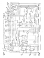
correction circuit 1. Thedigital delay line 10 is implemented using a serial chain of 1 of 2 data selectors (S0 - Sn). The selectors are non-inverting and can be implemented with NAND gates or with an equivalent such as AND-OR gates. Alogic 0 orlogic 1 on the bottom control lead selects thelogic 0 orlogic 1 input, respectively. The number of data selectors, n (not including S0), must be greater than the CLK REF period divided by the worst case minimum selector propagation delay. The Q outputs ofshift register 11 control the selectors of thedigital delay line 10. - The 360
degree phase detector 13 consists of a 360 degree positive edge detector includingflip flop 26, inverter 27, ANDgate 28, and an inhibit circuit which prevents false 360 degree phase detects. The inhibit circuit consists of a 0 DEG inhibit circuit comprised of Exclusive NORgate 29, ANDgate 31 andflip flop 32 and a 180 DEG inhibit circuit comprised ofgates flip flop 32. - The clock
correct control circuit 12A is a shift clock and direction control circuit consisting of gates and flipflops 33 through 45, which provides an asynchronous phase advance and phase retard signal interface to the limiteddata phase detector 3 via the ADV, RET and CLR CORRECT signals. Figure 4 shows an embodiment of aphase detector 3 which will be described hereinafter. - The shift overrun advance (SOA)
detector 16 detects a shift right overrun which starts the SOA sequencer via the SOA signal. The SOA detector consists of gates and flip flop 20-25. TheSOA sequencer 17 is a state machine which controls the clockcorrect control circuit 12A when searching for 360 degree delay. - The operation of the center frequency
phase correction circuit 1 of Figure 3 will now be described for (a) the reset state, (b) retard corrections from 0 to 180 degrees, (c) retard corrections from 180 to 360 degrees, (d) advance correction at 0 degrees and (e) advance corrections from 360 to 0 degrees. - If a reset pulse is applied to the
SOA sequencer 17, all its outputs are forced to 0 and BRESET pulses high which resets flip-flops shift register 11 outputs to alllogic 0's except for Q0 and Q1 which are set tologic 1. In the reset state the digital delay line output (DCLK) is just the BCLK REF signal delayed by the S0 selector "1" input-to-output path. This is the zero degree phase reference of DCLK for the 360 degreephase detector circuit 13. Since SOA is low, DCLK passes throughselector 15 to become UB CLK OUT. - Edge
detector shift register 26 samples the DCLK signal at its D input on the falling edge of the BCLK REF signal. In the reset condition, the edge detector typically samples thedigital delay line 10 output just before a falling edge. Theshift register 26 thus typically contains alllogic 1's, but due to worst case IC propagation delays alllogic 0's orsporadic logic 0's and 1's could occur. - The 0 DEG -INH output of NOR
gate 29 is low since Q0 & Q1 = 1. This forces the -INH lead low via ANDgate 31 and D flip-flop 32 after a negative edge of BCLK REF occurs. The 360 DEG DET lead is also forced low via ANDgate 28. Thus SR INIT is inhibited from pulsing high even if the edge detector detects positive edges. The state of the 180 DEG -INH lead is high, but is a "don't care" state since the output of ANDgate 31 is forced low by the 0 DEG -INH lead. - On the first negative BCLK REF edge after the RESET input goes low, A/R SHIFT CLK goes high. On the second negative BCLK REF edge after the RESET input goes low, CLR CORRECT goes low which removes the reset on Figure 4 flip-
flops - When a high phase retard signal is received on the RET input from the
phase detector 3, the l/-R input to shiftregister 11 goes "high" on the next negative edge of buffer clock reference (BCLK REF) setting up a left shift. A/R SHIFT CLK goes "low" on the next negative edge of BCLK REF causing SHIFT CLK to go "low" after passing throughselector 44 anddelay 45. This shifts a pair of logic "1's" inshift register 11 at taps Q0 and Q1 to taps Q1 and Q2 and places a logic "0" into Qo which causes selector S1 to insert a delay of dT in thedigital delay line 10 path from CLK REF to CLK OUT. All following rising and falling edges of CLK OUT will thus be delayed by an additional delay of dT. - The CLR CORRECT signal goes "high" on the third negative edge of BCLK REF to reset flip-
flops flops - Errors in the CLK OUT signal are avoided during insertion of the dT delay by not changing the Q0 output of
shift register 11 from logic "1" to logic "0" until both selector S0 inputs are at logic "0". This condition occurs after the BCLK REF "high" to "low" transition propagates through selector S1. Thedelay block 45 delay is chosen so that this condition is guaranteed under worst case conditions. The delay, if required, can be implemented with conventional inverters or gates. The leftmost logic "1" of the shifted pair of logic "1's" which was at Q1 before the shift, and now is at Q2, sets up the delay path which will be inserted upon each shift and completely isolates the digital delay line output from the data selector to the left. - Each new phase retard request received, causes the pair of "one's" in
shift register 11 to shift left one position which adds an additional dT of delay to the CLK OUT signal. When the pair of logic one's are shifted past Qx, the 0 DEG -INH line goes "high" since all logic "0's" are present on the inputs of NORgate 29. The output of ANDgate 31 then goes logic high assuming the 180 DEG -INH line is still high.After one CLK REF period, -INH goes high which enables the 360degree detector 13. - The Qx tap is chosen to inhibit a positive edge detect which otherwise might occur near zero degree phase and cause a shift register initialize (SR INIT) before 360 degree phase delay is reached. With worst case maximum selector propagation delays determine the Q output where 360 degree phase delay is selected. Qx is preferably selected to be about two taps before this tap. This ensures that the zero degree inhibit circuit will never mask valid 360 degree detects.
- Until CLK OUT is delayed by 180 degrees relative to BCLK REF, the edge
detector shift register 26 will sample logic "1's" and thus Q0 = Q1 = Q2 = 1. When 180 degree phase delay occurs, logic "0's" will be sampled and thus Q0 = Q1= Q2 = 0. The 180 degree inhibit circuit, comprised ofgates flip flop 32 and the illustrated resistor R and capacitor C inhibits positive edges which look like 360 degree phase detect edges (Q1 = 1, Q2 = 0) from causing a false SR INIT signal at 180 degrees instead of at 360 degrees delay. CLK REF jitter or variations in selector gate delays can cause the foregoing condition to occur. -
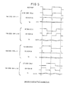
EX-NOR gate 30 monitors the phase of BCLK REF and DCLK and charges capacitor C via resistor R to the average DC output voltage. - Figure 5 shows the 180 degree inhibit circuit waveforms for the
states gate 31 and the -INH lead are logic low from about>90 degrees to<270 degrees of phase delay. This assumes that the input switching threshold of ANDgate 31 is at 2.5 volts. Input threshold variation will not affect the performance of the inhibit circuit, although the inhibit phase zone about 180 degrees will increase or decrease with a high or low threshold, respectively. The inhibit phase zone will never include the phase near 360 (or 0) degrees. This ensures that the 180 degree inhibit function will never mask valid 360 degree detects. Note that the 180 degree inhibit function can overlap with the 0 degree inhibit function and normally will do so with worst case maximum selector delays. - The RC time constant is chose such that it is large enough to maintain a valid logic low when near 180 degrees of phase delay but small enough to not mask the 360 degree detect during fast retard with a worst case maximum average selector delay (minimum number of shifts to 360 degrees).
- The EX-NOR, R and
C 180 degree inhibit circuit will always accurately mask the edge detects near 180 degrees whether 180 degrees is approached with phase advance or phase retard corrections. Even if no corrections occur and the delay line delay decreases from>180 degrees to<180 degrees due to temperature variations, the positive edge detect will be masked. An all digital 180 degree inhibit circuit would not perform as well. - As additional retard corrections occur and 360 degree phase delay is approached, the edge
detector shift register 26 outputs are 0 and the 360 degree detector is enabled. When Q1 ofshift register 26 goes tologic gate 28, OR gate 41 and ANDgate 40.Shift register 11 is initialized just as during reset with Q0 = Q1 = 1 and Q2 through Qn = 0. Taps Q0 and Q1 ofshift register 11force 0 DEG -INH low via NORgate 29. SR INIT returns low when flip-flop 32 samples the low output of ANDgate 31. The correction circuit has now completed a 0 to 360 and back to 0 degree phase cycle. The correction circuit is now ready for additional phase retard requests. - The Q0 output of
shift register 26 is not used to allow metastable states to settle out during one period of CLK REF. The DCLK is asychronous relative to the sampling clock, BCLK REF, due to the incremental delays of thedigital delay line 10. A metastable state could potentially delay the SR INIT pulse to occur after the BCLK REF returns high and cause an error condition in CLK OUT. - In order to avoid error conditions in CLK OUT, the BCLK REF input at the logic "1" inputs of selectors S1 and S0 must be low before the Q1 or Q0 outputs go high as a result of SR INIT pulsing high. The inherent worst case minimum delays of gates, flip flop and register 26, 28, 41, 40 and 11 respectively typically provide an adequate total delay to compensate for maximum high-to-low transition time of BCLK REF, input threshold differences or layout variations.
- An advance request at 0 degrees requires that one CLK REF period delay be found to allow shift advance corrections to occur without overrunning the end of the
shift register 11. This is done by performing a fast retard shift under the control of the shift overrun-advance (SOA)sequencer 17. - When a high advance signal is received on the ADV input from
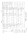
phase detector 3, the L/-R input to shiftregister 11 stays low setting up a right shift. The A/R SHIFT CLK goes low on the next negative edge of BCLK REF causing SHIFT CLK to go low after passing throughselector 44 anddelay 45. This shifts the logic "1" at Q0 ofshift register 11 to flip-flop 25 viagates gate 22 and ANDgate 23 until RES SOA goes high.Selector 15 connects BCLK REF to unbuffered clock out (UB CLK OUT). Flip-flop 37 is also set to hold CLR CORRECT low until the RES SOA signal goes high. - Figure 6 shows the timing as waveform diagrams for the
SOA sequencer 17. TheSOA sequencer 17 begins its control sequence when the SOA signal goes high. The basic operation of theSOA sequencer 17 is as follows: - (1) SOA goes high.
- (2) SR INIT C pulses high for one CLK REF period to initialize
shift register 11. - (3) While SR INIT C is high, FAST SHIFT goes high which connects the SHIFT CLK to BCLK REF via
selector 44 anddelay 45. RET S also goes high which sets flip-flop 34 (Q = R*), resulting in L/-R ofshift register 11 going high. - (4) When SR INIT C returns low, INH SR INIT goes high to prevent shift register initialization when 360 degree delay is reached.
- (5) The next negative edge of SHIFT CLK after SR INIT C goes low, shifts the pair of 1's at Q1 and Q0 left by one tap. Each following negative edge of SHIFT CLK again shifts the pair of 1's left by one tap. While this fast retard shift occurs. CLK OUT remains connected to CLK REF via
buffer 9,selector 15 andbuffer 14. - (6) The fast retard shift continues with the 0 and 180 degree inhibit circuits functioning as described earlier. When the 360 DEG DET line pulses high, RET S goes low and flip-flop 34 (Q = R*) is reset via
OR gate 43. The SR INIT does not occur at this time as INH SR INIT is still high. - (7) The next four negative edges of SHIFT CLK shift the pair of one's in
shift register 11 right four taps. This compensates for the over-shoot which occurs due to the inherent two cycle delay in detecting 360 degree phase delay and ensures that DCLK will be early relative to BCLK REF so that with worst case gate delays, the 360 degree phase detector will not detect 360 degree delay. - (8) FAST SHIFT goes low when the fourth right SHIFT CLK occurs which forces SHIFT CLK low to stop shifting of
shift register 11. - (9) RES SOA pulses high on the positive edge of BCLK REF before the fourth negative edge of SHIFT CLK occurs. When the fourth negative edge of SHIFT CLK occurs, SOA goes low which switches
selector 15 to DCLK. No errors will occur during this switch since both BCLK REF and DCLK are low when the switch occurs. - (10) The set to flip-
flop 37 goes low with SOA and on the next negative edge of BCLK REF the CLR CORRECT line goes high and clears the ADV and RET signals from the phase detector. - (11) INH SR INIT goes low a half cycle after SOA goes low to enable a future 360 degree detect to produce an SR INIT.
- (12) When CLR CORRECT returns low the clock correct control circuit is ready to receive another ADV or RET correction.
- A maximum of n + 11 CLK REF periods are required to complete the 360 degree phase retard search, where n is the number of selectors less one. In most applications this delay will not significantly affect clock correction accuracy, particularly when K of the divide by
K circuit 2 of Figure 1 is large. - Advance corrections from 360 to 0 degrees are performed essentially in the same manner as retard corrections except that the pair of logic one's in
shift register 11 are shifted to the right instead of left. Each right shift removes a selector delay dT, which causes DCLK to advance relative to BCLK REF. The 0 to 180 degree inhibit circuits function the same as previously described for retard corrections. - Referring now to Figure 4 A, a
phase detector 3 which attempts to center the negative edge of the RECEIVE CLK between incoming or limited data transitions is shown. It is to be understood that this is only an example of one type of phase detector which may be used with the present invention. Figure 4B shows the phase detector timing. Data flip-flops sample 1′) edges of the RECEIVE CLK, respectively as illustrated. The three samples are provided to a logic circuit comprised ofgates 53 to 57 for evaluation and the result is output as a phase ADV or phase RET information signal upon the negative update edge of the RECEIVE CLK. Flip-flops gates - If
sample 1 is different thansample 2, the RECEIVE CLK is early and the RET output goes high on the update sample. Ifsample 2 is different fromsample 1′, the RECEIVE CLK is late and the ADV output goes high on the update sample. The foregoing is illustrated by the Fig. 4B waveforms. In both cases the samples on either side of the center sample must be different or else phase ADV and phase RET remain low. This maintains improved center sampling and prevents unnecessary ADV - RET corrections when the limited data has bias distortion eg., where + data pulses are wider than - data pulses or vice versa. - The RECEIVE CLK is corrected in increments of dT to maintain the negative edge of RECEIVE CLK approximately centered between limited data transitions. The
shift register 11 of the center frequency phase-lock loop will shift the pair of logic "1's" left or right as required to phase-lock the RECEIVE CLK to the incoming LIMITED DATA. - One preferred application of the center frequency phase-lock loop of the present invention shown in Figures 1 through 4 is in a Manchester data clock recovery circuit. This application uses the capability of the center frequency phase-lock loop to make small phase corrections to the output clock which is at the same frequency as the input CLK REF frequency. Referring again to Figure 1, 6.528 M bps limited Manchester data may be provided to
phase detector 3. A 13.056 Mhz crystal can be used to generate CLK REF with a worst case duty cycle of 40-60%. CLK OUT is then divided by K = 1 to yield the RECEIVE CLK. With reference to Figure 3, the typical selector delay is assumed as 4 nsec +/- 80% including process, temperature and voltage variations. The minimum and maximum selector delays are thus 0.8 nsec and 7.2 nsec, respectively. - The number of selectors required is determined by dividing the CLK REF period by the minimum selector delay or 76.593 nsec/.8 nsec = 95.7. An actual embodiment would use 97 selectors minimum to be on the safe side, so n = 97. The Qx tap is determined by dividing the CLK REF period by the maximum selector delay and subtracting two for a safety margin. Thus 76.593 nsec/7.2 nsec - 2 = 10.6 -2 = 8.6. Qx would then equal Q8 to be on the safe side. The RC time constant of the 180 degree inhibit circuit should be approximately 100 nsec. The RC circuit values of R = 4 pF and C = 25K ohm would be appropriate.
- The accuracy of center sampling is dependent on the duty cycle of CLK REF. With a 60-40% duty cycle a +/- 10% sampling error can occur. The
digital delay line 10 will not degrade the duty cycle of CLK REF at CLK OUT even if the selector NAND gate high-to-low and low-to-high propagation delays are not equal. Since two NAND gates are used in each selector, each selector has a total delay equal to the low-to-high plus high-to-low propagation delays for either type of input transition. If very accurate center sampling is required, CLK OUT should be divided by 2 (K=2) to eliminate any duty cycle inaccuracy. This of course doubles the required input frequency at CLK REF. - Another preferred embodiment and application of the present invention is an ISDN U interface clock recovery at the line terminal (LT),and ideally requires that CLK OUT be phase locked between 0 and 360 degrees relative to the CLK REF input with no jitter. Occasional small phase steps are required to track the slowly changing phase of the limited data transitions from the network terminals due primarily to cable temperature variations. The present invention is well suited for this application. The IC technology employed provides that the maximum selector delay provides an acceptably small phase step (<1/1000 baud period). This ensures that the far end signal from the network terminal NT can be extracted from a signal which also includes the near end line terminal LT transmitted and echo signals with a minimum of error.
- Typically examplary ISDN U interface clock recovery specifications are:
Transmission Echo canceller with hybrid Line 2B1Q Rcv baud rate 80 K +/- 5 ppm CLK REF freq (f) 10.24 Mhz (+/-10 ppm) CLK REF period 97.652 nsec (40-60% duty cycle) CLK OUT (f) 10.24 Mhz +/- 5 ppm (when phase locked) divide by K (fig. 1) K=128 RECEIVE CLK freq. 80 Khz +/- 5 ppm RECEIVE CLK period 12.5 usec 2 u CMOS selector delay 4 nsec +/- 80% (0.8 nsec min, 7.2 nsec - For the aforementioned application, LIMITED DATA as shown in Fig. 1 is actually zero crossing transition information from the four level 2B1Q signal derived via a zero crossing comparator. The
phase detector 3 can be implemented with the circuit shown in Figure 4A. An averaging advance-retard counter circuit can be inserted between thephase detector 3 and center frequency phase-lock loop 1 to output only one correction request every few seconds. This provides the ability to track slow LIMITED DATA phase shifts due to cable temperature variations, while not following the high frequency jitter from the far end (NT). - To provide compatibility with the aforementioned Manchester data clock recovery circuit and also operation over CLK REF frequencies of 10 Mhz to 15 Mhz the number of selectors is chosen to equal 127 and Qx = Q7, R equals 25K ohms and C equals 4pF.
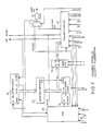
- Figure 7 shows a block diagram of a clock correct control circuit with gate delay compensation (12B). This clock correct control circuit can be used in place of the
circuit 12 shown in Figure 3 to provide the additional features of gate delay compensation, bandwidth mode control, andshift register 11 all zero's recovery. - Gate delay compensation reduces the worst case min-max dT correction range to 1:2 or better by using multiple dT corrections to build up the minimum dT correction. Bandwidth mode control allows control over the min-max correction range.
Shift register 11 all zero's recovery prevents an all zero's lock-up state. - Gate delay compensation of the phase-lock loop is required in many applications to provide a tighter tolerance correction. Since there is no high frequency reference to base each correction on, as in a conventional digital phase-lock loop, another approach must be taken. First the average selector propagation delay can be determined by counting the number of net retard shifts necessary to provide one CLK REF period delay. The average selector delay is then just the CLK REF period divided by this count. The desired minimum correction time is divided by this average selector delay to provide the number of dT corrections necessary to achieve this time. The minimum correction time must be greater than half the maximum dT correction. The worst case correction time accuracy covers a 1:2 min-max range regardless of the IC gate delay variation. The following equations summarize the above description and illustrate how the division operation can be simplified.

- INT(x/y) means the integer portion only of x/y after the division. To simplify the division implementation, the desired minimum correction time should be chosen to yield a 1/2**n result for MIN CORRECT TIME/CLK REF PERIOD in Eq. (3) where n is an integer. Simple binary division of AVG NET RET COUNT can then be performed by shifting left n times toward the most significant bit.
- The block diagram of Figure 7 illustrates a technique which uses binary division to compensate for gate delay variations. Average
net retard counter 64 holds the average number ofshift register 11 shift left-minus-right clocks required to go from 0 to 360 degree delay. This up/down counter is incremented or decremented one count each time SR INIT or RES SOA occurs vialogic 65. Just before SR INIT or RES SOA occurs, thenet retard counter 62 count A is compared to the average net retard counter count B bymagnitude comparator 63. If A: B, then the average net retard count is incremented, otherwise it is decremented. The three most significant bits of the average net retard count (B6-B4) are provided to amode control circuit 66. A binary divide-by-16 of B6-B0 is accomplished by using only B6-B4 which is equivalent to shifting left four bits. - The mode control circuit maps B6-B4 to P2-P0 based on the C and D inputs. B6-B4 is passed straight through (CD=11), divided by 2 (CD=10), divided by 4 (CD=01), or divided by 8 (CD=00). Divide by 8 just results in P2=P1=P0=0 which is the
narrowband mode 0. A programmableshift count generator 67 translates the P2-P0 input to the appropriate number of shift clocks for each phase advance or phase retard request. The binary count of P2-P0 plus 1 equals the number of shift clocks.Mode 0 is equivalent to no gate delay compensation since only one shift clock occurs for each correction. - The clock correct control circuit of Fig. 7 can also be used in
mode 0 for the Manchester data or ISDN LT clock recovery applications. Gate delay compensation is not required for either of these applications since even the worst case minimum phase step is still sufficient to track the data. - If 128 net retards have occured with no SR INIT or RES SOA, then shift
register 11 must be in an undesired "all zero's" state. In this state A7 goes high and vialogic 65 generates an SR INIT and resets the twocounters shift register 11. - The SOA sequencer used with the clock
correct control circuit 12 B requires a special power-up circuit. This circuit quickly establishes the correct average net retard count even with a limited data transition source which is close in frequency to CLK REF. This start-up circuit forces the fast shift mode for 128 x 128 = 16,384 periods of CLK REF. This allows sufficient shift clocks to update the average net retard counter to its full count with a worst case minimum selector delay. - The circuit of Figure 7 is based on a range of .8 to 7.2 nsec selector delays and a minimum CLK REF frequency of 10 Mhz. The counter sizes, mode control operation and programmable shift count generator can be modified for other applications.
- A clock recovery application for an ISDN U interface at the network terminal (NT) illustrates the technique used for gate delay compensation and mode control. Requirements are similar to clock recovery at the line terminal (LT), except that a minimum correction of about 6 nsec is required to track the data under minimum transition and maximum jitter conditions. A maximum of 12.2 nsec results due to the
worst case 1 to 2 range for gate delay compensation. This is still less than the maximum correction limit of about 1/1000 baud period (12.5 nsec).
Substituting in the first fraction of Eq. (3):
- Then approximate 1/16.2 with 1/16 = 1/2**4 to allow division to be implemented by a shift left 4 x and substitute in Eq. (3):
INT(1/16* AVG RET COUNT)+1 = NO. OF dT CORRECTIONS - Table 1 shows the max and min average selector delay (dT), B6 B5 B4 and the no. of dT corrections for any average retard count from 0 to 127. This table is derived from Eq. (1) and the above.
- Tables 2A through 2D show B6 B5 B4, P2 P1 P0, the number of shift clocks per retard request and the correct time for
modes Mode 0 is equivalent to clockcorrect control circuit 12A in Figure 3 since only one shift clock is generated per retard request regardless of the average selector delay. Themode 0 correct time range is .769 to 7.2 nsec which is a 1:9.4 range.Modes 1 to 3 reduce the correction time range by increasing the minimum correction time:Mode 0 =.769 - 7.2 nsec, 1:9.4 Mode 1 =1.538 - 7.2 nsec, 1:4.7 Mode 2 =3.076 - 7.2 nsec, 1:2.3 Mode 3 =6.152 - 12.2 nsec, 1:2 - The
mode 3 correction time range meets the requirements for clock recovery at the network terminalTABLE 1 AVG RET COUNT AVG SELECTOR DELAY B6 B5 B4 NO. OF dT CORRECTS MAX(NS) MIN(NS) 0 - 15 - 6.510 0 0 0 1 16 - 31 6.100 3.150 0 0 1 2 32 - 47 3.052 2.078 0 1 0 3 48 - 63 2.035 1.550 0 1 1 4 64 - 79 1.526 1.236 1 0 0 5 80 - 95 1.221 1.028 1 0 1 6 96 - 111 1.017 .880 1 1 0 7 112 - 127 .872 .769 1 1 1 8 TABLE 2A (MODE 0, AB=00) B6 B5 B4 P2 P1 P0 SHIFT CLKS CORRECT TIME MAX(ns) MIN(ns) 0 0 0 0 0 0 1 (7.2) 6.510 0 0 1 0 0 0 1 6.100 3.150 0 1 0 0 0 0 1 3.052 2.078 0 1 1 0 0 0 1 2.035 1.550 1 0 0 0 0 0 1 1.526 1.236 1 0 1 0 0 0 1 1.221 1.028 1 1 0 0 0 0 1 1.017 .880 1 1 1 0 0 0 1 .872 .769 TABLE 2B (MODE 1, AB=01) B6 B5 B4 P2 P1 P0 SHIFT CLKS CORRECT TIME MAX(ns) MIN(ns) 0 0 0 0 0 0 1 (7.2) 6.510 0 0 1 0 0 0 1 6.100 3.150 0 1 0 0 0 0 1 3.052 2.078 0 1 1 0 0 0 1 2.035 1.550 1 0 0 0 0 1 2 3.052 2.472 1 0 1 0 0 1 2 2.442 2.056 1 1 0 0 0 1 2 2.034 1.760 1 1 1 0 0 1 2 1.744 1.538 TABLE 2C (MODE 2, AB=10) B6 B5 B4 P2 P1 P0 SHIFT CLKS CORRECT TIME MAX(ns) MIN(ns) 0 0 0 0 0 0 1 (7.2) 6.510 0 0 1 0 0 0 1 6.100 3.150 0 1 0 0 0 1 2 6.104 4.156 0 1 1 0 0 1 2 4.070 3.100 1 0 0 0 1 0 3 4.578 3.708 1 0 1 0 1 0 3 3.663 3.084 1 1 0 0 1 1 4 4.068 3.520 1 1 1 0 1 1 4 3.488 3.076 TABLE 2D (MODE 3, AB=11) B6 B5 B4 P2 P1 P0 SHIFT CLKS CORRECT TIME MAX(ns) MIN(ns) 0 0 0 0 0 0 1 (7.2) 6.510 0 0 1 0 0 1 2 12.200 6.300 0 1 0 0 1 0 3 9.156 6.234 0 1 1 0 1 1 4 8.140 6.200 1 0 0 1 0 0 5 7.630 6.180 1 0 1 1 0 1 6 7.326 6.168 1 1 0 1 1 0 7 7.119 6.160 1 1 1 1 1 1 8 6.976 6.152 - While the present invention has been described in connection with a preferred embodiment thereof, other embodiments and applications will become apparent to those skilled in the art. For example, an alternative implementation of the center frequency high resolution digital phase locked loop reduces the 360 degree search time after SOA occurs. This consists of initializing
shift register 11 only on power up. Retard corrections occur as described earlier except thatshift register 11 R2 - Rn reset inputs are never pulsed during SR INIT, only S1 and S0. During phase advance corrections, a pair of logic "1's" are injected at the left end ofshift register 11 at SRD based on the average net phase retard count. Each time SOA occurs, a pair of logic "1's" will be near 360 degrees of phase delay and an advance-retard search algorithm locates 360 degrees. In this approach it is difficult to recover from undesired shift register states. - There are many other applications of the invention besides the low speed optic fiber and ISDN clock recovery circuits described herein. High speed fiber optic data and clock recovery circuits can also be implemented if high speed IC technology is used. For example a 500 Mbit/sec NRZ clock recovery circuit could be designed using a 500 Mhz CLK REF input to a gallium arsenide IC implementation of the invention. On-chip 100 psec selector delays would provide a resolution of 20 samples per bit. A conventional digital phase locked loop would require a very high 10 Ghz CLK REF input. The invention can be used in any application where a DPLL can be used without the requirement of a high frequency reference. A T1 1.544 Mhz clock recovery circuit can also be implemented using the invention with an appropriate phase detector and gate delay compensated correction time.
- The invention can also be used to implement a delay line with delay based on a clock reference. The delay is established by a programmable percentage of the average net retard count. IC process delay variations are compensated for upon initialization, and periodic calibration cycles compensate for temperature and voltage changes. The foregoing is all included within the spirit and scope of the invention as set forth by the claims appended hereto.
Claims (24)
digital phase correction means, having coupled thereto an input clock reference signal with a frequency f, and coupled therefrom a clock output phase-locked frequency, where f, is centered at said output phase locked frequency;
divided-by-K circuit means for dividing said clock output phase-locked frequency by an integer K, to derive a data receive clock phase-locked to incoming data transitions;
phase detector means having said data receive clock an said incoming data coupled thereto for generating phase correction signals whenever said data receive clock does not coincide in time with said incoming data transitions, and for coupling said phase correction signals to said digital phase correction means to selectively introduce a fixed delay in said clock output phase locked frequency, such that said clock output phase locked frequency equals said clock reference signal frequency;
said phase detector means including means for generating phase correction signals which are either phase advance or phase retard signals respectively, when said data receive clock is either late or early, respectively, with respect to said incoming data transitions;
wherein said digital phase correction means includes means for resetting said phase advance or phase retard signals after the phase of said clock output signal is corrected and a digital delay line means for providing an incremental delay from 0 to 360 degrees of the period of said clock reference signal; and
shift register means for selecting a desired incremental delay from said delay line; and
clock correction control means for controlling said shift register means in accordance with said phase advance and phase retard signals to select said incremental delay from said delay line.
the smallest increment of said incremental delay is the propagation delay of two serially connected logic gates in said digital delay line.
three hundred sixty degree phase detection circuit means for initializing said shift register means when the output of said digital delay line has been phase retarded by 360 degrees, such that said digital delay line functions as an infinite delay line while providing only one clock period of actual delay.
shift overrun advance detector means for detecting phase advance overshoot condition, and for overriding phase correction signals in response to sequencer control signals; and
shift overrun advance sequencer means for generating said sequencer control signals to enable a selector means to modify the clock output frequency to compensate for said phase advance overshoot condition, such that an apparent infinite delay line is provided for both phase advance and phase retard corrections.
means for providing a digital delay line reset;
means for providing phase retard correction signals from 0 to 180 degrees;
means for providing phase retard correction signals from 180 degrees to 360 degrees;
means for providing phase advance correction signals from 0 to 180 degrees;
means for providing phase advance correction signals from 180 to 360 degrees.
inhibit circuit means for tracking gate delay variations when no shift clocks are present.
buffer amplifier means for providing a buffered clock reference to drive said digital delay line.
said digital delay line is comprised of a serial chain of non-inverting NAND or equivalent logic gates.
means for centering the negative edge of a received clock between the data transitions of incoming data.
digital phase correction means, having coupled thereto an input clock reference signal with a frequency f, and coupled therefrom a clock output phase locked frequency, where f, is centered at said output phase locked frequency;
divide-by-K circuit means for dividing said clock output phase-locked frequency by an integer K, to derive a data receive clock phase-locked to incoming data transitions, said incoming data being 2B1Q line code for providing zero crossing transition information;
phase detector means having said data receive clock and said incoming data coupled thereto for generating phase correction signals whenever said data receive clock does not coincide in time with said incoming data transitions, and for coupling said phase corrections signals to said digital phase correction means to selectively introduce a predetermined delay in said clock output phase locked frequency, such that said clock output phase locked frequency equals said clock reference signal frequency and means for tracking phase shifts in said incoming data due to cable temperature variations, while not following high frequency jitter.
an averaging phase advance-phase retard counter for deriving correction requests once every several seconds.
Applications Claiming Priority (2)
| Application Number | Priority Date | Filing Date | Title |
|---|---|---|---|
| US07/149,459 US4789996A (en) | 1988-01-28 | 1988-01-28 | Center frequency high resolution digital phase-lock loop circuit |
| US149459 | 1988-01-28 |
Publications (2)
| Publication Number | Publication Date |
|---|---|
| EP0326007A2 true EP0326007A2 (en) | 1989-08-02 |
| EP0326007A3 EP0326007A3 (en) | 1990-10-17 |
Family
ID=22530370
Family Applications (1)
| Application Number | Title | Priority Date | Filing Date |
|---|---|---|---|
| EP19890100813 Withdrawn EP0326007A3 (en) | 1988-01-28 | 1989-01-18 | Center frequency high resolution digital phase-loop circuit |
Country Status (3)
| Country | Link |
|---|---|
| US (1) | US4789996A (en) |
| EP (1) | EP0326007A3 (en) |
| NO (1) | NO890378L (en) |
Cited By (2)
| Publication number | Priority date | Publication date | Assignee | Title |
|---|---|---|---|---|
| AU614138B2 (en) * | 1988-06-03 | 1991-08-22 | Alcatel N.V. | A bit clock recovery method |
| CN101562450B (en) * | 2008-04-16 | 2012-07-18 | 北京兆易创新科技有限公司 | Gradually approaching delay phase-locked loop circuit and method for adjusting clock signal |
Families Citing this family (69)
| Publication number | Priority date | Publication date | Assignee | Title |
|---|---|---|---|---|
| US4964118A (en) * | 1988-10-24 | 1990-10-16 | Northern Telecom Limited | Apparatus and method for echo cancellation |
| US5087829A (en) * | 1988-12-07 | 1992-02-11 | Hitachi, Ltd. | High speed clock distribution system |
| GB8924202D0 (en) * | 1989-10-27 | 1989-12-13 | Ncr Co | Digital phase lock loop decoder |
| US5012494A (en) * | 1989-11-07 | 1991-04-30 | Hewlett-Packard Company | Method and apparatus for clock recovery and data retiming for random NRZ data |
| FR2658015B1 (en) * | 1990-02-06 | 1994-07-29 | Bull Sa | LOCKED PHASE CIRCUIT AND RESULTING FREQUENCY MULTIPLIER. |
| US5109394A (en) * | 1990-12-24 | 1992-04-28 | Ncr Corporation | All digital phase locked loop |
| US5295164A (en) * | 1991-12-23 | 1994-03-15 | Apple Computer, Inc. | Apparatus for providing a system clock locked to an external clock over a wide range of frequencies |
| US5451894A (en) * | 1993-02-24 | 1995-09-19 | Advanced Micro Devices, Inc. | Digital full range rotating phase shifter |
| JP3247190B2 (en) * | 1993-04-13 | 2002-01-15 | 三菱電機株式会社 | Phase locked loop circuit and integrated circuit device |
| US5552726A (en) * | 1993-05-05 | 1996-09-03 | Texas Instruments Incorporated | High resolution digital phase locked loop with automatic recovery logic |
| US5506874A (en) * | 1993-11-01 | 1996-04-09 | Texas Instruments Incorporated | Phase detector and method |
| JP2704103B2 (en) * | 1993-11-09 | 1998-01-26 | 日本電気エンジニアリング株式会社 | Phase comparison circuit |
| US5515403A (en) * | 1994-06-21 | 1996-05-07 | Dsc Communications Corporation | Apparatus and method for clock alignment and switching |
| US5828250A (en) * | 1994-09-06 | 1998-10-27 | Intel Corporation | Differential delay line clock generator with feedback phase control |
| JPH0884161A (en) * | 1994-09-13 | 1996-03-26 | Fuji Electric Co Ltd | Reception detecting circuit device for serial communication equipment using bi-phase code |
| US5796673A (en) * | 1994-10-06 | 1998-08-18 | Mosaid Technologies Incorporated | Delay locked loop implementation in a synchronous dynamic random access memory |
| JP3561792B2 (en) * | 1995-09-06 | 2004-09-02 | 株式会社ルネサステクノロジ | Clock generation circuit |
| JP2926651B2 (en) * | 1995-11-02 | 1999-07-28 | 株式会社鷹山 | Matched filter circuit |
| JPH09307407A (en) * | 1996-05-09 | 1997-11-28 | Internatl Business Mach Corp <Ibm> | Clock oscillator, clock generator circuit and oscillating method for clock pulse |
| US5991609A (en) * | 1996-12-26 | 1999-11-23 | Delco Electronics Corporation | Low cost digital automatic alignment method and apparatus |
| US5974105A (en) * | 1997-03-13 | 1999-10-26 | Industrial Technology Research Institute | High frequency all digital phase-locked loop |
| CA2204089C (en) * | 1997-04-30 | 2001-08-07 | Mosaid Technologies Incorporated | Digital delay locked loop |
| US5990719A (en) * | 1997-10-07 | 1999-11-23 | Intel Corporation | Adaptive filtering scheme for sampling phase relations of clock networks |
| US6075832A (en) * | 1997-10-07 | 2000-06-13 | Intel Corporation | Method and apparatus for deskewing clock signals |
| US6084933A (en) * | 1997-11-17 | 2000-07-04 | Advanced Micro Devices, Inc. | Chip operating conditions compensated clock generation |
| JP3048134B2 (en) * | 1997-12-02 | 2000-06-05 | 日本電気株式会社 | Clock signal regeneration device |
| US6069506A (en) * | 1998-05-20 | 2000-05-30 | Micron Technology, Inc. | Method and apparatus for improving the performance of digital delay locked loop circuits |
| US6069507A (en) * | 1998-05-22 | 2000-05-30 | Silicon Magic Corporation | Circuit and method for reducing delay line length in delay-locked loops |
| KR100295052B1 (en) * | 1998-09-02 | 2001-07-12 | 윤종용 | Delay locked loop including a controller capable of changing a number of unit delay in voltage controlled delay line |
| EP0987853A1 (en) | 1998-09-17 | 2000-03-22 | STMicroelectronics S.r.l. | A fully digital phase aligner |
| KR100301048B1 (en) | 1998-10-19 | 2001-09-06 | 윤종용 | Delay lock loop having variable stage and operating method |
| US6415008B1 (en) | 1998-12-15 | 2002-07-02 | BéCHADE ROLAND ALBERT | Digital signal multiplier |
| JP3292169B2 (en) * | 1999-02-24 | 2002-06-17 | 日本電気株式会社 | Semiconductor integrated circuit |
| IT1311463B1 (en) * | 1999-12-31 | 2002-03-12 | Cit Alcatel | METHOD OF RECOVERY OF THE CLOCK SIGNAL IN A SYSTEM OF TELECOMMUNICATIONS AND RELATED CIRCUIT. |
| US6774693B2 (en) * | 2000-01-18 | 2004-08-10 | Pmc-Sierra, Inc. | Digital delay line with synchronous control |
| US6273251B1 (en) * | 2000-04-24 | 2001-08-14 | Tim Rust | Travel protector for golf club heads |
| US6950487B2 (en) * | 2001-05-18 | 2005-09-27 | Micron Technology, Inc. | Phase splitter using digital delay locked loops |
| US7062004B1 (en) * | 2001-06-06 | 2006-06-13 | Silicon Image, Inc. | Method and apparatus for adaptive control of PLL loop bandwidth |
| DE10149584B4 (en) | 2001-10-08 | 2007-11-22 | Infineon Technologies Ag | Delay locked loop |
| DE10149585C2 (en) * | 2001-10-08 | 2003-11-20 | Infineon Technologies Ag | Integrable, controllable delay device, use of a delay device and method for operating a delay device |
| US7221723B2 (en) * | 2001-11-27 | 2007-05-22 | Agilent Technologies, Inc. | Multi-phase sampling |
| US7546097B2 (en) * | 2002-03-06 | 2009-06-09 | Qualcomm Incorporated | Calibration techniques for frequency synthesizers |
| US20030194046A1 (en) * | 2002-04-11 | 2003-10-16 | Shirar Jerry Lester | Method for period counting using a tunable oscillator |
| US7098707B2 (en) * | 2004-03-09 | 2006-08-29 | Altera Corporation | Highly configurable PLL architecture for programmable logic |
| KR100713082B1 (en) * | 2005-03-02 | 2007-05-02 | 주식회사 하이닉스반도체 | Delay locked loop for controlling duty rate of clock |
| GB2452748A (en) * | 2007-09-13 | 2009-03-18 | Cambridge Silicon Radio Ltd | Digital phase locked loop |
| US7893788B2 (en) * | 2008-02-19 | 2011-02-22 | Mediatek Inc. | Charge pump-based frequency modulator |
| JP4562787B2 (en) * | 2008-07-30 | 2010-10-13 | ルネサスエレクトロニクス株式会社 | PLL circuit |
| JP4787870B2 (en) * | 2008-10-02 | 2011-10-05 | 日本電波工業株式会社 | Frequency synthesizer |
| GB0821772D0 (en) * | 2008-11-28 | 2009-01-07 | Zarlink Semiconductor Inc | Soft reference switch for phase locked loop |
| CN101764608B (en) * | 2008-12-25 | 2012-07-04 | 北京兆易创新科技有限公司 | Bit-by-bit approaching delay phase-locked loop circuit and method for regulating input clock signal |
| US7973612B2 (en) * | 2009-04-26 | 2011-07-05 | Qualcomm Incorporated | Supply-regulated phase-locked loop (PLL) and method of using |
| US8169265B2 (en) * | 2009-04-29 | 2012-05-01 | Mediatek Inc. | Phase lock loop circuits |
| US8368480B2 (en) * | 2009-06-24 | 2013-02-05 | Mediatek Inc. | Phase locked loop circuits and gain calibration methods thereof |
| CN101964658B (en) * | 2009-07-23 | 2012-10-17 | 财团法人工业技术研究院 | Digital phase-locked loop and digital-phase frequency detector thereof |
| CN102045061B (en) * | 2009-10-16 | 2013-04-24 | 晨星软件研发(深圳)有限公司 | Loop bandwidth control device and method of phase locked loop |
| CN102045064B (en) * | 2009-10-20 | 2013-03-13 | 群联电子股份有限公司 | Phase locked loop and voltage controlled oscillator |
| CN102104376B (en) * | 2009-12-16 | 2013-05-22 | 晨星软件研发(深圳)有限公司 | Phase generation device and phase generation method |
| CN102158227B (en) * | 2010-02-11 | 2013-04-17 | 奇景光电股份有限公司 | Non-integer N type phase-locked loop |
| JP4933635B2 (en) * | 2010-02-19 | 2012-05-16 | 日本電波工業株式会社 | PLL circuit |
| CN102307047B (en) * | 2010-06-01 | 2013-04-24 | 钰创科技股份有限公司 | Circuit and method for generating clock pulse data reply signal phase locked index |
| CN101860361B (en) * | 2010-06-03 | 2012-05-09 | 无锡中星微电子有限公司 | Delay-locked loop |
| CN101951260B (en) * | 2010-10-11 | 2012-10-17 | 上海电力学院 | Digital delay phase locked loop circuit |
| US8400199B2 (en) * | 2010-11-26 | 2013-03-19 | Mediatek Inc. | Charge pump, phase frequency detector and charge pump methods |
| CN102185607B (en) * | 2011-01-25 | 2013-11-06 | 上海华为技术有限公司 | Phase difference detection method, device and circuit in phase-locked loop circuit |
| CN102130680B (en) * | 2011-03-30 | 2013-05-08 | 苏州麦格芯微电子有限公司 | Temperature compensation type crystal oscillator and communication method thereof |
| CN102130679B (en) * | 2011-04-12 | 2013-01-30 | 广州润芯信息技术有限公司 | Active RC (Resistance-Capacitance) filter bandwidth calibration method |
| CN102299709A (en) * | 2011-04-27 | 2011-12-28 | 广州润芯信息技术有限公司 | High precision pulse width comparator based on time-to-digit conversion |
| DE102012216326B4 (en) | 2012-09-13 | 2020-06-18 | TRUMPF Hüttinger GmbH + Co. KG | RF power inverter system |
Citations (3)
| Publication number | Priority date | Publication date | Assignee | Title |
|---|---|---|---|---|
| US3509471A (en) * | 1966-11-16 | 1970-04-28 | Communications Satellite Corp | Digital phase lock loop for bit timing recovery |
| EP0157701A2 (en) * | 1984-03-29 | 1985-10-09 | Fujitsu Limited | Phase synchronization circuit |
| EP0240232A2 (en) * | 1986-04-01 | 1987-10-07 | Hewlett-Packard Company | Digital phase lock loop |
Family Cites Families (3)
| Publication number | Priority date | Publication date | Assignee | Title |
|---|---|---|---|---|
| US4418318A (en) * | 1981-03-10 | 1983-11-29 | Frederick Electronics Corporation | Digital phase-locked loop circuit |
| US4385396A (en) * | 1981-06-05 | 1983-05-24 | Phillips Petroleum Company | NRZ Digital data recovery |
| US4574243A (en) * | 1984-01-03 | 1986-03-04 | Motorola, Inc. | Multiple frequency digital phase locked loop |
-
1988
- 1988-01-28 US US07/149,459 patent/US4789996A/en not_active Expired - Lifetime
-
1989
- 1989-01-18 EP EP19890100813 patent/EP0326007A3/en not_active Withdrawn
- 1989-01-30 NO NO89890378A patent/NO890378L/en unknown
Patent Citations (3)
| Publication number | Priority date | Publication date | Assignee | Title |
|---|---|---|---|---|
| US3509471A (en) * | 1966-11-16 | 1970-04-28 | Communications Satellite Corp | Digital phase lock loop for bit timing recovery |
| EP0157701A2 (en) * | 1984-03-29 | 1985-10-09 | Fujitsu Limited | Phase synchronization circuit |
| EP0240232A2 (en) * | 1986-04-01 | 1987-10-07 | Hewlett-Packard Company | Digital phase lock loop |
Non-Patent Citations (3)
| Title |
|---|
| IEEE INTERNATIONAL CONFEREENCE ON COMMUNICATIONS, Seattle, Washington, 7th - 10th June 1987, vol. 1, paper 18.2, pages 596-600, IEEE, New York, US; M. FUKIDA et al.: "An echo canceller LSI for ISDN subscriber loop transmission" * |
| IEEE TRANS. CIRCUITS & SYST., vol. CAS-25, no. 4, April 1978, pages 222-228; W.C. LEUNG: "Optimum LSI implementation for a digital phase-locked loop" * |
| INTERNATIONAL SWITCHING SYMPOSIUM, Phoenix, Arizona, 15th - 20th March 1987, pages 571-576, IEEE, New York, US; R. DIERCKX et al.: "ITT VLSI chip set for ISDN" * |
Cited By (2)
| Publication number | Priority date | Publication date | Assignee | Title |
|---|---|---|---|---|
| AU614138B2 (en) * | 1988-06-03 | 1991-08-22 | Alcatel N.V. | A bit clock recovery method |
| CN101562450B (en) * | 2008-04-16 | 2012-07-18 | 北京兆易创新科技有限公司 | Gradually approaching delay phase-locked loop circuit and method for adjusting clock signal |
Also Published As
| Publication number | Publication date |
|---|---|
| NO890378D0 (en) | 1989-01-30 |
| US4789996A (en) | 1988-12-06 |
| EP0326007A3 (en) | 1990-10-17 |
| NO890378L (en) | 1989-07-31 |
Similar Documents
| Publication | Publication Date | Title |
|---|---|---|
| US4789996A (en) | Center frequency high resolution digital phase-lock loop circuit | |
| US4847870A (en) | High resolution digital phase-lock loop circuit | |
| US6584163B1 (en) | Shared data and clock recovery for packetized data | |
| US4821297A (en) | Digital phase locked loop clock recovery scheme | |
| US4584695A (en) | Digital PLL decoder | |
| US6760389B1 (en) | Data recovery for non-uniformly spaced edges | |
| US5412697A (en) | Delay line separator for data bus | |
| US7844021B2 (en) | Method and apparatus for clock skew calibration in a clock and data recovery system using multiphase sampling | |
| US4527277A (en) | Timing extraction circuit | |
| US7170964B2 (en) | Transition insensitive timing recovery method and apparatus | |
| US6236697B1 (en) | Clock recovery for multiple frequency input data | |
| CA1308448C (en) | Method of and circuit arrangement for recovering a bit clock from a received digital communication signal | |
| US5644605A (en) | Jitter attenuator | |
| US6389090B2 (en) | Digital clock/data signal recovery method and apparatus | |
| EP0228021B1 (en) | Improvements to digital phase-locked loop circuits | |
| US5751775A (en) | Transmission circuit of a line encoded signal on a telephone line | |
| US5717728A (en) | Data/clock recovery circuit | |
| EP1474900A2 (en) | Cmi signal timing recovery | |
| US5058142A (en) | Clock extracting circuit in digital-line signal receiver | |
| EP1006660B1 (en) | Clock reproduction and identification apparatus | |
| EP0176561B1 (en) | Digital phase-locked loop circuit | |
| EP0732830A2 (en) | Circuit for clock signal extraction from a high speed data stream | |
| US5127026A (en) | Circuit and method for extracting clock signal from a serial data stream | |
| WO1999025066A1 (en) | Phase lock loop for synchronous reference clocks | |
| KR100265309B1 (en) | Method of and arrangement for generating a clock signal from a biphase modulated digital signal |
Legal Events
| Date | Code | Title | Description |
|---|---|---|---|
| PUAI | Public reference made under article 153(3) epc to a published international application that has entered the european phase |
Free format text: ORIGINAL CODE: 0009012 |
|
| AK | Designated contracting states |
Kind code of ref document: A2 Designated state(s): AT BE CH DE ES FR GB GR IT LI NL SE |
|
| PUAL | Search report despatched |
Free format text: ORIGINAL CODE: 0009013 |
|
| AK | Designated contracting states |
Kind code of ref document: A3 Designated state(s): AT BE CH DE ES FR GB GR IT LI NL SE |
|
| 17P | Request for examination filed |
Effective date: 19901220 |
|
| 17Q | First examination report despatched |
Effective date: 19930205 |
|
| STAA | Information on the status of an ep patent application or granted ep patent |
Free format text: STATUS: THE APPLICATION IS DEEMED TO BE WITHDRAWN |
|
| 18D | Application deemed to be withdrawn |
Effective date: 19930616 |