EP0325423B1 - An error detecting circuit for a decoder - Google Patents
An error detecting circuit for a decoder Download PDFInfo
- Publication number
- EP0325423B1 EP0325423B1 EP89300436A EP89300436A EP0325423B1 EP 0325423 B1 EP0325423 B1 EP 0325423B1 EP 89300436 A EP89300436 A EP 89300436A EP 89300436 A EP89300436 A EP 89300436A EP 0325423 B1 EP0325423 B1 EP 0325423B1
- Authority
- EP
- European Patent Office
- Prior art keywords
- circuit
- node
- input node
- output
- units
- Prior art date
- Legal status (The legal status is an assumption and is not a legal conclusion. Google has not performed a legal analysis and makes no representation as to the accuracy of the status listed.)
- Expired - Lifetime
Links
- 238000001514 detection method Methods 0.000 claims description 21
- 238000011144 upstream manufacturing Methods 0.000 claims description 2
- 238000010586 diagram Methods 0.000 description 4
- 239000000470 constituent Substances 0.000 description 1
- 230000000644 propagated effect Effects 0.000 description 1
- 239000004065 semiconductor Substances 0.000 description 1
Images


Classifications
-
- G—PHYSICS
- G06—COMPUTING; CALCULATING OR COUNTING
- G06F—ELECTRIC DIGITAL DATA PROCESSING
- G06F11/00—Error detection; Error correction; Monitoring
- G06F11/07—Responding to the occurrence of a fault, e.g. fault tolerance
- G06F11/0703—Error or fault processing not based on redundancy, i.e. by taking additional measures to deal with the error or fault not making use of redundancy in operation, in hardware, or in data representation
- G06F11/0751—Error or fault detection not based on redundancy
- G06F11/0763—Error or fault detection not based on redundancy by bit configuration check, e.g. of formats or tags
-
- G—PHYSICS
- G06—COMPUTING; CALCULATING OR COUNTING
- G06F—ELECTRIC DIGITAL DATA PROCESSING
- G06F11/00—Error detection; Error correction; Monitoring
- G06F11/07—Responding to the occurrence of a fault, e.g. fault tolerance
- G06F11/08—Error detection or correction by redundancy in data representation, e.g. by using checking codes
- G06F11/085—Error detection or correction by redundancy in data representation, e.g. by using checking codes using codes with inherent redundancy, e.g. n-out-of-m codes
Definitions
- the present invention relates to an error detecting circuit for a decoder having a plurality of output terminals and producing an active logic level at one output terminal in response to an input selection data.
- Such a decoder has been employed in a register selection circuit of a microprocessor or in a semiconductor memory as an address decoder.
- the decoder employed in the register selection circuit has a plurality of output terminals connected respectively to read/write enable terminals of a plurality of registers and outputs the active level to one of the output terminals in response to the selection data applied thereto, thus selecting a corresponding one of the registers. Data is thereby written into or read from the selected register.
- the active logic level is outputted at two or more output terminals in response to a single selection data. The corresponding two or more registers are thereby selected simultaneously, so that the contents stored in these registers are outputted simultaneously or the same data is written into two or more registers simultaneously.
- US-A-3.886.520 discloses a checking circuit for a 1-out-of- n decoder in which a binary table of rows and columns is established.
- Column associated 0-OR and 1-OR gates have their outputs coupled to ⁇ 1-OR and >1-OR gates to indicate that two or more, or none, of the decoder outputs is active.
- an object of the present invention is to provide a decoder error detecting circuit for detecting whether or not a decoder operates correctly.
- Another object of the present invention is to provide an error detection circuit for a decoder to detect whether or not two or more output terminals of the decoder take the active logic level in response to the same selection data.
- an error detection circuit for a decoder having a plurality of decoded output terminals, said error detection circuit comprising a set of first circuit units, each including a first input node, a first selection input node, a first output node, means for connecting said first input node to said first output node when said first selection input node is at a first logic level, and means for outputting a predetermined logic level to said first output node when said first selection input node is at a second logic level; a set of second circuit units, each including a second input node, a third input node, a second selection input node, a second output node, means for connecting said second input node to said second output node when said second selection input node is at said first logic level, and means for controlling a logic level of said second output node in response to the logic level of said third input node when second selection input node is at said second logic level; means connecting said first circuit units in series such that the first output node of the preced
- an error output signal is taken from the output terminal of the last series-connected second circuit unit.
- the associated two or more circuit units receive the active level at the respective selection input nodes.
- the first one of those associated circuit units outputs the predetermined logic level at its first output node, so that the second one of them outputs the predetermined logic level at its second output node.
- the predetermined logic level is propagated at the second output node of the last circuit unit, and the error detection signal is produced to indicate an incorrect operation of the decoder.
- the decoder may produce the active level at two or more output terminals in response to the same selection data
- a register selection circuit 500 includes a decoder 541 and sixteen registers 500 to 515.
- the decoder 541 has four input terminals I0 to I3 supplied with a 4-bits select data and sixteen output terminals O0 to O15 which are in turn connected to read/write enable terminals ET of the registers 500 to 515, respectively.
- an active level a high level or logic "1” in this description
- the remaining output terminals are held at an inactive level (i.e., a low level or logic "0").
- the decoder 541 fails or operates incorrectly, it outputs the active level at two or more output terminals thereof. For this reason, the corresponding two or more registers are selected and coupled to the data bus 539.
- an error detection circuit 540 is provided in accordance with the present invention. This circuit 540 is connected to the output terminals O0 to O15 of the decoder 541 and produces at a terminal 150 an error signal ERR when at least two output terminals of the decoder 541 take the active level simultaneously.
- the error detection circuit 540 includes fifteen first-type detecting circuits 120-0 to 120-14 and sixteen second-type detecting circuits 100-0 to 100-15.
- Each of the first-type detecting circuits 120-0 to 120-14 has an input node 121, an output node 123 and a selection input node 122.
- the selection nodes 122 of the detecting circuit 120-0 to 120-14 are connected to the first to fifteen output terminals O0 to O14 of the decoder 541, respectively.
- the first-type detecting circuits 120-0 to 120-14 are connected in series such that the output node 123 of the preceding circuit is connected to the input node 121 of the subsequent circuit.
- any one of the first-type detecting circuit 120-0 to 120-14 receives at its selection input node 122 the active level from the associated output terminal of the decoder 541, it produces the low level (logic "0") at its output node 123 irrespective of the logic level at its input node 121 to inform the subsequent detecting circuit 120 of receiving the active level from the decoder 541.
- the first-type detecting circuit or circuits 120 receiving the inactive level at the selection input node 122 transfer the logic level at the input node 121 to the output node 123. Since the detecting circuit 120-0 is the leading stage, the input node 121 thereof is fixed at logic "1" of Vcc level.
- Each of the second-type detecting circuits 100-0 to 100-15 has first and second input nodes 101 and 102, an output node 104 and a selection input node 103. These second-type detecting circuits 100-0 to 100-15 are connected in series such that the output node 104 of the preceding circuit is connected to the first input node 101 of the subsequent circuit.
- the selection input nodes 102 of the second-type detecting circuits 100-0 to 100-15 are connected to the output terminals O0 to O15 of the decoder 541, respectively.
- the second input nodes 102 of the second-type detecting circuits 100-1 to 100-15 except the leading circuit 100-0 are connected to the output nodes 123 of the first-type detecting circuits 120-0 to 120-14, respectively.
- the detecting circuit 100-0 Since the detecting circuit 100-0 is the leading circuit, the first and second input nodes 101 and 102 thereof are connected to Vcc terminal to receive logic "1".
- the second-type detecting circuit 100-0 to 100-15 receives at its selection input node 103 the active level from the associated output terminal of the decoder 541, it controls the logic level of its output node 104 in response to the logic level at its second input node 102.
- the output node 104 is controlled to be at the high level.
- the output node 104 In case where the second input node 102 is at the low level (logic "0"), the output node 104 is controlled to be at the low level.
- the second-type detecting circuit or circuits 100 receiving the inactive level at the selection node 103 from the decoder 541 transfer the logic level at the first input node 101 to the output node 104.
- An inverter 141 is connected between the error output terminal 150 and the final second-type detecting circuit 100-15. Therefore, the error detection signal ERR taking logic "1" indicates that the decoder 541 produces the active level at two or more output terminals simultaneously.
- the detecting circuit 120-1 thereby outputs logic "0" at its output node 123, so that more significant detecting circuits 120-2 to 120-14 also produce logic "0" at the respective output nodes 123. Only the circuit 120-0 produce logic "1" at its output node 123.
- the detecting circuit 100-1 responds the active level of the output terminal O1 to control its output node 104 in response to the logic level at its second input node 102.
- the error detection signal ERR takes logic "1" to indicate the incorrect operation of the decoder 541. More specifically, in response to the active level of the second output terminal O1, the output nodes 123 of the detecting circuit 120-1 to 120-14 all becomes to logic "0". Since the fifteenth output terminal O14 is also at the active level, the detecting circuit 100-14 controls the logic level of its output node 104 in response to the logic level at its second input node 102. Since logic "0" is applied thereto, the output node 104 of the detecting circuit 100-14 becomes to logic "0". This logic level, logic "0", is transferred to the inverter 141 via the circuit 100-15. As a result, the signal ERR takes logic "1".
- the error detection circuit 540 shown in Fig. 2 can be detect whether or not the decoder 541 operates correctly.
- Each of the first-type detecting circuit 120-0 to 120-14 and the second-type detecting circuits 100-0 to 100-15 having the above-mentioned functions can be constituted by various static-type and/or dynamic-type gate circuits.
- One example of each of the first-type detecting circuits 120-0 to 120-15 is shown in Fig. 3A and one example of each of the second-type detecting circuits 100-0 to 100-15 is shown in Fig. 3B.
- each of the first-type detecting circuits 120-0 to 120-14 includes an AND gate 204 and an inverter 205 which are connected as shown.
- each of the second-type detecting circuits 100-0 to 100-15 includes an OR gate 202, an AND gate 201 and an inverter 203 which are connected as shown. Therefore, when the node 103 receives the active level, the output node 104 is controlled by the logic level at the second input node 102. In case where the node 104 receives the inactive level, on the other hand, the AND gate 201 is made open to transfer the logic level at the first input node 101 to the output node 104.
- Fig. 4 Such an error detection circuit is shown in Fig. 4 as a second embodiment of the present invention, in which the same constituents as those shown in Fig. 1 are denoted by like reference numerals to omit the further description thereof.
- Fig. 4 a second set of sixteen second-type detecting circuits 100-16 to 100-31 are additionally provided and connected as shown, in cascade with the first set of second circuits 100-0 to 100-14.
- the inverter 141 is connected between the error detection output terminals 150 and the additionally provided sixteenth second-type detecting circuit 100-31.
- the signal ERR takes the logic "1" when the active level appears at three or more of decoded output terminals O0 to O15.
Description
- The present invention relates to an error detecting circuit for a decoder having a plurality of output terminals and producing an active logic level at one output terminal in response to an input selection data.
- Such a decoder has been employed in a register selection circuit of a microprocessor or in a semiconductor memory as an address decoder. For example, the decoder employed in the register selection circuit has a plurality of output terminals connected respectively to read/write enable terminals of a plurality of registers and outputs the active level to one of the output terminals in response to the selection data applied thereto, thus selecting a corresponding one of the registers. Data is thereby written into or read from the selected register. However, if the decoder is faulty, the active logic level is outputted at two or more output terminals in response to a single selection data. The corresponding two or more registers are thereby selected simultaneously, so that the contents stored in these registers are outputted simultaneously or the same data is written into two or more registers simultaneously.
- US-A-3.886.520 (Christensen) discloses a checking circuit for a 1-out-of-n decoder in which a binary table of rows and columns is established. Column associated 0-OR and 1-OR gates have their outputs coupled to <1-OR and >1-OR gates to indicate that two or more, or none, of the decoder outputs is active.
- Therefore, an object of the present invention is to provide a decoder error detecting circuit for detecting whether or not a decoder operates correctly.
- Another object of the present invention is to provide an error detection circuit for a decoder to detect whether or not two or more output terminals of the decoder take the active logic level in response to the same selection data.
- According to the present invention, there is provided an error detection circuit for a decoder having a plurality of decoded output terminals, said error detection circuit comprising a set of first circuit units, each including a first input node, a first selection input node, a first output node, means for connecting said first input node to said first output node when said first selection input node is at a first logic level, and means for outputting a predetermined logic level to said first output node when said first selection input node is at a second logic level; a set of second circuit units, each including a second input node, a third input node, a second selection input node, a second output node, means for connecting said second input node to said second output node when said second selection input node is at said first logic level, and means for controlling a logic level of said second output node in response to the logic level of said third input node when second selection input node is at said second logic level; means connecting said first circuit units in series such that the first output node of the preceding first circuit unit is connected to the first input node of the subsequent first circuit unit; means connecting said second circuit units in series such that the second output node of the preceding second circuit unit is connected to the second input node of the subsequent circuit unit; the first input node and the second input node of the leading first and second circuit units respectively each being connected to a fixed logic level; means connecting the first output node of each of said first circuit units to the third input node of the associated one of said second circuit units; means connecting said first and second selection input nodes of said first and second circuit units to the corresponding one of said decoded output terminals; and means connecting the third input node of the leading one of said second circuit units to the first input node of the leading one of said first circuit units.
- In one embodiment an error output signal is taken from the output terminal of the last series-connected second circuit unit.
- If the decoder operates incorrectly to output the active level at two or more output terminals in response to a single selection data, the associated two or more circuit units receive the active level at the respective selection input nodes. The first one of those associated circuit units outputs the predetermined logic level at its first output node, so that the second one of them outputs the predetermined logic level at its second output node. As a result, the predetermined logic level is propagated at the second output node of the last circuit unit, and the error detection signal is produced to indicate an incorrect operation of the decoder.
- In another embodiment for use if the decoder may produce the active level at two or more output terminals in response to the same selection data, there are a plurality of sets of second circuit units arranged in cascade, the units of each set being connected in series with each other and being connected to units of the immediately upstream set of first circuit units or second circuit units in the manner specified above for the first mentioned set of second circuit units, an error output signal being taken from the output terminal of the last series-connected second circuit unit of the most downstream set of second circuit units.
- The above and other objects, advantages and features of the present invention will be more apparent from the following description taken in conjunction with the accompanying drawings, in which:
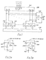
- Fig. 1 is a block diagram showing a register selection circuit of a microprocessor as an example of application of an error detection circuit according to the present invention;
- Fig. 2 is a block diagram showing an error detection circuit according to a first embodiment of the present invention;
- Figs. 3A and 3B are gate circuit diagrams representing an example of first-type and second-type detection circuits shown in Fig. 2, respectively; and
- Fig. 4 is a block diagram representative of a second embodiment of the present invention.
- Referring to Fig. 1, a
register selection circuit 500 includes adecoder 541 and sixteenregisters 500 to 515. Thedecoder 541 has four input terminals I₀ to I₃ supplied with a 4-bits select data and sixteen output terminals O₀ to O₁₅ which are in turn connected to read/write enable terminals ET of theregisters 500 to 515, respectively. When thedecoder 541 operates correctly, it outputs an active level (a high level or logic "1" in this description) at one of the output terminals O₀ to O₁₅ in response to the selection data, as shown in TABLE-1. The remaining output terminals are held at an inactive level (i.e., a low level or logic "0").TABLE 1 Selection Data Output Terminal Taking Active Level I₀ (LSB) I₁ I₂ I₃ (MSB) 0 0 0 0 O₀ 1 0 0 0 O₁ 0 1 0 0 O₂ 1 1 0 0 O₃ 0 0 1 0 O₄ 1 0 1 0 O₅ 0 1 1 0 O₆ 1 1 1 0 O₇ 0 0 0 1 O₈ 1 0 0 1 O₉ 0 1 0 1 O₁₀ 1 1 0 1 O₁₁ 0 0 1 1 O₁₂ 1 0 1 1 O₁₃ 0 1 1 1 O₁₄ 1 1 1 1 O₁₅
By referring to TABLE-1, when the content of the selection data is "1000", for example, the second output terminal O₁ takes the active level. Theregister 501 is thereby selected and coupled to adata bus 539. Thus, the data stored in theregister 501 is read onto thedata bus 539 or the data on thebus 539 is written into theregister 501. - However, if the
decoder 541 fails or operates incorrectly, it outputs the active level at two or more output terminals thereof. For this reason, the corresponding two or more registers are selected and coupled to thedata bus 539. - In order to detect whether or not the
decoder 541 operates correctly, anerror detection circuit 540 is provided in accordance with the present invention. Thiscircuit 540 is connected to the output terminals O₀ to O₁₅ of thedecoder 541 and produces at aterminal 150 an error signal ERR when at least two output terminals of thedecoder 541 take the active level simultaneously. - Referring to Fig. 2, the
error detection circuit 540 according to an embodiment of the present invention includes fifteen first-type detecting circuits 120-0 to 120-14 and sixteen second-type detecting circuits 100-0 to 100-15. Each of the first-type detecting circuits 120-0 to 120-14 has aninput node 121, anoutput node 123 and aselection input node 122. Theselection nodes 122 of the detecting circuit 120-0 to 120-14 are connected to the first to fifteen output terminals O₀ to O₁₄ of thedecoder 541, respectively. The first-type detecting circuits 120-0 to 120-14 are connected in series such that theoutput node 123 of the preceding circuit is connected to theinput node 121 of the subsequent circuit. When any one of the first-type detecting circuit 120-0 to 120-14 receives at itsselection input node 122 the active level from the associated output terminal of thedecoder 541, it produces the low level (logic "0") at itsoutput node 123 irrespective of the logic level at itsinput node 121 to inform the subsequent detecting circuit 120 of receiving the active level from thedecoder 541. On the other hand, the first-type detecting circuit or circuits 120 receiving the inactive level at theselection input node 122 transfer the logic level at theinput node 121 to theoutput node 123. Since the detecting circuit 120-0 is the leading stage, theinput node 121 thereof is fixed at logic "1" of Vcc level. - Each of the second-type detecting circuits 100-0 to 100-15 has first and
second input nodes output node 104 and aselection input node 103. These second-type detecting circuits 100-0 to 100-15 are connected in series such that theoutput node 104 of the preceding circuit is connected to thefirst input node 101 of the subsequent circuit. Theselection input nodes 102 of the second-type detecting circuits 100-0 to 100-15 are connected to the output terminals O₀ to O₁₅ of thedecoder 541, respectively. Thesecond input nodes 102 of the second-type detecting circuits 100-1 to 100-15 except the leading circuit 100-0 are connected to theoutput nodes 123 of the first-type detecting circuits 120-0 to 120-14, respectively. Since the detecting circuit 100-0 is the leading circuit, the first andsecond input nodes selection input node 103 the active level from the associated output terminal of thedecoder 541, it controls the logic level of itsoutput node 104 in response to the logic level at itssecond input node 102. When thesecond input node 102 is at the high level (logic "1"), theoutput node 104 is controlled to be at the high level. In case where thesecond input node 102 is at the low level (logic "0"), theoutput node 104 is controlled to be at the low level. On the other hand, the second-type detecting circuit orcircuits 100 receiving the inactive level at theselection node 103 from thedecoder 541 transfer the logic level at thefirst input node 101 to theoutput node 104. Aninverter 141 is connected between theerror output terminal 150 and the final second-type detecting circuit 100-15. Therefore, the error detection signal ERR taking logic "1" indicates that thedecoder 541 produces the active level at two or more output terminals simultaneously. - Next, description on the operation of the circuit shown in Fig. 2 will be made below. Assume first that the
decoder 541 operates correctly to respond the selection data of "1000" to produce the active level only the second output terminal O₁ with holding the remaining output terminals O₀ and O₂ to O₁₅ at the inactive level. The detecting circuit 120-1 thereby outputs logic "0" at itsoutput node 123, so that more significant detecting circuits 120-2 to 120-14 also produce logic "0" at therespective output nodes 123. Only the circuit 120-0 produce logic "1" at itsoutput node 123. The detecting circuit 100-1 responds the active level of the output terminal O₁ to control itsoutput node 104 in response to the logic level at itssecond input node 102. Ib this case, since logic "1" is applied thereto, theoutput node 103 of the circuit 100-1 takes logic "1". Since the output terminals O₂ to O₁₅ of thedecoder 541 is at the inactive level, logic "1" at theoutput node 104 of the circuit 100-1 is transferred to theinverter 141 via the circuits 100-2 to 100-15. As a result, the signal ERR takes logic "0" to indicate the correct operation of thedecoder 541. - On the other hand, if the
decoder 541 operates incorrectly to produce the active level at two output terminals O₁ and O₁₄ in response to the selection data of "1000", the error detection signal ERR takes logic "1" to indicate the incorrect operation of thedecoder 541. More specifically, in response to the active level of the second output terminal O₁, theoutput nodes 123 of the detecting circuit 120-1 to 120-14 all becomes to logic "0". Since the fifteenth output terminal O₁₄ is also at the active level, the detecting circuit 100-14 controls the logic level of itsoutput node 104 in response to the logic level at itssecond input node 102. Since logic "0" is applied thereto, theoutput node 104 of the detecting circuit 100-14 becomes to logic "0". This logic level, logic "0", is transferred to theinverter 141 via the circuit 100-15. As a result, the signal ERR takes logic "1". - Thus, the
error detection circuit 540 shown in Fig. 2 can be detect whether or not thedecoder 541 operates correctly. - Each of the first-type detecting circuit 120-0 to 120-14 and the second-type detecting circuits 100-0 to 100-15 having the above-mentioned functions can be constituted by various static-type and/or dynamic-type gate circuits. One example of each of the first-type detecting circuits 120-0 to 120-15 is shown in Fig. 3A and one example of each of the second-type detecting circuits 100-0 to 100-15 is shown in Fig. 3B. Referring to Fig. 3A, each of the first-type detecting circuits 120-0 to 120-14 includes an AND
gate 204 and aninverter 205 which are connected as shown. Accordingly, when theselection node 122 receives the active level (logic "1"), theoutput node 123 takes logic "0" irrespective of the level at theinput node 121. On the other hand, when theselection node 122 receives the inactive level (logic "0"), the ANDgate 204 is made open to transfer the logic level at theinput node 121 to theoutput node 123. Referring to Fig, 3B, each of the second-type detecting circuits 100-0 to 100-15 includes an ORgate 202, an ANDgate 201 and aninverter 203 which are connected as shown. Therefore, when thenode 103 receives the active level, theoutput node 104 is controlled by the logic level at thesecond input node 102. In case where thenode 104 receives the inactive level, on the other hand, the ANDgate 201 is made open to transfer the logic level at thefirst input node 101 to theoutput node 104. - Some decoders produce the active level at two output terminals in response to the same selection data. In this case, an error detection circuit is required to detect whether or not the decoder produces the active level at three or more output terminals simultaneously. Such an error detection circuit is shown in Fig. 4 as a second embodiment of the present invention, in which the same constituents as those shown in Fig. 1 are denoted by like reference numerals to omit the further description thereof. In Fig. 4 a second set of sixteen second-type detecting circuits 100-16 to 100-31 are additionally provided and connected as shown, in cascade with the first set of second circuits 100-0 to 100-14. The
inverter 141 is connected between the errordetection output terminals 150 and the additionally provided sixteenth second-type detecting circuit 100-31. Thus, the signal ERR takes the logic "1" when the active level appears at three or more of decoded output terminals O₀ to O₁₅. By providing further the second-type detecting circuits 100, it is possible to detect whether the decoder produces the active level at four or more output terminals. - The invention is only limited by the apended claims. The above-mentioned embodiments are given by way of example only.
Claims (5)
- An error detection circuit for a decoder having a plurality of decoded output terminals (O1 to O15), said error detection circuit comprising:
a set of first circuit units (120-0 to 120-14), each including a first input node (121), a first selection input node (122), a first output node (123), means for connecting (204,205) said first input node (121) to said first output node (123) when said first selection input node (122) is at a first logic level, and means for outputting (204,205) a predetermined logic level to said first output node (123) when said first selection input node (122) is at a second logic level;
a set of second circuit units (100-0 to 100-15), each including a second input node (101), a third input node (102), a second selection input node (103), a second output node (104), means for connecting (201,202,203) said second input node (101) to said second output node (104) when said second selection input node (103) is at said first logic level, and means for controlling (201,202,203) a logic level of said second output node (104) in response to the logic level of said third input node (102) when second selection input node (103) is at said second logic level;
means connecting said first circuit units (120-0 to 120-14) in series such that the first output node (123) of the preceding first circuit unit is connected to the first input node (121) of the subsequent first circuit unit;
means connecting said second circuit units (100-0 to 100-15) in series such that the second output node (104) of the preceding second circuit unit is connected to the second input node (101) of the subsequent circuit unit;
the first input node (121) and the second input node (101) of the leading first and second circuit units respectively each being connected to a fixed logic level;
means connecting the first output node (123) of each of said first circuit units (120-0 to 120-14) to the third input node (102) of the associated one of said second circuit units (100-0 to 100-15);
means connecting said first and second selection input nodes (122,103) of said first and second circuit units (120-0 to 120-14, 100-0 to 100-15) to the corresponding one of said decoded output terminals; and
means connecting the third input node (102) of the leading one of said second circuit units (100-0 to 100-15) to the first input node (121) of the leading one of said first circuit units. - An error detection circuit as claimed in Claim 1 wherein an error output signal (15) is taken from the output terminal of the last series-connected second circuit unit (100-15).
- An error detection circuit as claimed in Claim 1 wherein there are a plurality of sets of second circuit units (100-0 to 100-15 and 100-16 to 100-31) arranged in cascade, the units of each set being connected in series with each other and being connected to units of the immediately upstream set of first circuit units or second circuit units in the manner specified in Claim 1 for the first mentioned set of second circuit units, an error output signal (150) being taken from the output terminal of the last series-connected second circuit unit (100-31) of the most downstream set of second circuit units.
- An error detection circuit as claimed in any preceding claim, wherein each of said first circuit units (120-0 to 120-14) includes an AND circuit (204) having a first input end connected to said first input node (121), a second input end connected via a first inverter (205) to said first selection input node (122) and an output end connected to said first output node (123).
- An error detection circuit as claimed in any preceding claim, wherein each of said second circuit units (100-0 to 100-15) includes an OR circuit (202) and an AND circuit (201), said OR circuit (202) having a first input end connected to said third input node (102) and a second input end connected via a second inverter (203) to said second selection input node (103), said AND circuit (201) having a first input end connected to said second input node (101), a second input end connected to an output end of said OR circuit (202) and an output end connected to said second node (104).
Applications Claiming Priority (2)
| Application Number | Priority Date | Filing Date | Title |
|---|---|---|---|
| JP63008765A JPH07120954B2 (en) | 1988-01-18 | 1988-01-18 | Decoder error detection circuit |
| JP8765/88 | 1988-01-18 |
Publications (3)
| Publication Number | Publication Date |
|---|---|
| EP0325423A2 EP0325423A2 (en) | 1989-07-26 |
| EP0325423A3 EP0325423A3 (en) | 1990-03-21 |
| EP0325423B1 true EP0325423B1 (en) | 1993-11-24 |
Family
ID=11702007
Family Applications (1)
| Application Number | Title | Priority Date | Filing Date |
|---|---|---|---|
| EP89300436A Expired - Lifetime EP0325423B1 (en) | 1988-01-18 | 1989-01-18 | An error detecting circuit for a decoder |
Country Status (4)
| Country | Link |
|---|---|
| US (1) | US4949343A (en) |
| EP (1) | EP0325423B1 (en) |
| JP (1) | JPH07120954B2 (en) |
| DE (1) | DE68910838T2 (en) |
Families Citing this family (4)
| Publication number | Priority date | Publication date | Assignee | Title |
|---|---|---|---|---|
| JP2513514Y2 (en) * | 1989-12-04 | 1996-10-09 | カシオ計算機株式会社 | Decoding circuit |
| JPH03189736A (en) * | 1989-12-19 | 1991-08-19 | Nec Corp | Fault detecting system for selection circuit |
| GB9421552D0 (en) * | 1994-10-26 | 1994-12-14 | Philips Electronics Uk Ltd | Improvements in or relating to data communication |
| US5995016A (en) * | 1996-12-17 | 1999-11-30 | Rambus Inc. | Method and apparatus for N choose M device selection |
Family Cites Families (5)
| Publication number | Priority date | Publication date | Assignee | Title |
|---|---|---|---|---|
| US3744024A (en) * | 1972-01-03 | 1973-07-03 | Stromberg Carlson Corp | Circuit for detecting the presence of other than one-bit-out-of-n bits |
| US3886520A (en) * | 1974-04-03 | 1975-05-27 | Sperry Rand Corp | Checking circuit for a 1-out-of-n decoder |
| US4087786A (en) * | 1976-12-08 | 1978-05-02 | Bell Telephone Laboratories, Incorporated | One-bit-out-of-N-bit checking circuit |
| US4320512A (en) * | 1980-06-23 | 1982-03-16 | The Bendix Corporation | Monitored digital system |
| US4380813A (en) * | 1981-04-01 | 1983-04-19 | International Business Machines Corp. | Error checking of mutually-exclusive control signals |
-
1988
- 1988-01-18 JP JP63008765A patent/JPH07120954B2/en not_active Expired - Lifetime
-
1989
- 1989-01-18 US US07/298,369 patent/US4949343A/en not_active Expired - Lifetime
- 1989-01-18 EP EP89300436A patent/EP0325423B1/en not_active Expired - Lifetime
- 1989-01-18 DE DE89300436T patent/DE68910838T2/en not_active Expired - Fee Related
Also Published As
| Publication number | Publication date |
|---|---|
| US4949343A (en) | 1990-08-14 |
| EP0325423A3 (en) | 1990-03-21 |
| DE68910838D1 (en) | 1994-01-05 |
| JPH07120954B2 (en) | 1995-12-20 |
| DE68910838T2 (en) | 1994-03-17 |
| EP0325423A2 (en) | 1989-07-26 |
| JPH01183919A (en) | 1989-07-21 |
Similar Documents
| Publication | Publication Date | Title |
|---|---|---|
| US5644583A (en) | Soft error correction technique and system for odd weight row error correction codes | |
| US4884271A (en) | Error checking and correcting for read-modified-write operations | |
| EP0096782B1 (en) | Online realignment of memory faults | |
| EP0336435A2 (en) | Memory diagnostic apparatus and method | |
| JPS6112292B2 (en) | ||
| US5331645A (en) | Expandable digital error detection and correction device | |
| JPS62117200A (en) | Unchanged memory | |
| US3898443A (en) | Memory fault correction system | |
| EP0096780B1 (en) | A fault alignment exclusion method to prevent realignment of previously paired memory defects | |
| US7246257B2 (en) | Computer system and memory control method thereof | |
| EP0096779A2 (en) | Multi-bit error scattering arrangement to provide fault tolerant semiconductor memory | |
| EP0325423B1 (en) | An error detecting circuit for a decoder | |
| JP2953737B2 (en) | Semiconductor memory having a multi-bit parallel test circuit | |
| EP0189699A2 (en) | Interdigitated bit line ROM | |
| EP0333214A2 (en) | Comparator unit for data discrimination | |
| JPS62242258A (en) | Storage device | |
| KR0156608B1 (en) | Semiconductor memory device having redundancy serial acess memory portion | |
| JPS5877100A (en) | Storage device | |
| JPS58200351A (en) | Error correcting circuit | |
| JPH0638239B2 (en) | Error correction mechanism | |
| JPH0423048A (en) | Error detection/correction integrated circuit, error detection/correction circuit, and data processor | |
| JPH0746517B2 (en) | Semiconductor memory and its testing method | |
| JPS61110247A (en) | Storage device | |
| GB2158622A (en) | Computer controlled systems | |
| RU1795520C (en) | Semiconductor on-line storage with correction of information |
Legal Events
| Date | Code | Title | Description |
|---|---|---|---|
| PUAI | Public reference made under article 153(3) epc to a published international application that has entered the european phase |
Free format text: ORIGINAL CODE: 0009012 |
|
| 17P | Request for examination filed |
Effective date: 19890130 |
|
| AK | Designated contracting states |
Kind code of ref document: A2 Designated state(s): DE FR GB |
|
| PUAL | Search report despatched |
Free format text: ORIGINAL CODE: 0009013 |
|
| RHK1 | Main classification (correction) |
Ipc: H03M 13/02 |
|
| AK | Designated contracting states |
Kind code of ref document: A3 Designated state(s): DE FR GB |
|
| 17Q | First examination report despatched |
Effective date: 19920127 |
|
| GRAA | (expected) grant |
Free format text: ORIGINAL CODE: 0009210 |
|
| AK | Designated contracting states |
Kind code of ref document: B1 Designated state(s): DE FR GB |
|
| PG25 | Lapsed in a contracting state [announced via postgrant information from national office to epo] |
Ref country code: FR Effective date: 19931124 |
|
| REF | Corresponds to: |
Ref document number: 68910838 Country of ref document: DE Date of ref document: 19940105 |
|
| EN | Fr: translation not filed | ||
| PLBE | No opposition filed within time limit |
Free format text: ORIGINAL CODE: 0009261 |
|
| STAA | Information on the status of an ep patent application or granted ep patent |
Free format text: STATUS: NO OPPOSITION FILED WITHIN TIME LIMIT |
|
| 26N | No opposition filed | ||
| REG | Reference to a national code |
Ref country code: GB Ref legal event code: IF02 |
|
| PGFP | Annual fee paid to national office [announced via postgrant information from national office to epo] |
Ref country code: GB Payment date: 20020116 Year of fee payment: 14 |
|
| PGFP | Annual fee paid to national office [announced via postgrant information from national office to epo] |
Ref country code: DE Payment date: 20020227 Year of fee payment: 14 |
|
| PG25 | Lapsed in a contracting state [announced via postgrant information from national office to epo] |
Ref country code: GB Free format text: LAPSE BECAUSE OF NON-PAYMENT OF DUE FEES Effective date: 20030118 |
|
| PG25 | Lapsed in a contracting state [announced via postgrant information from national office to epo] |
Ref country code: DE Free format text: LAPSE BECAUSE OF NON-PAYMENT OF DUE FEES Effective date: 20030801 |
|
| GBPC | Gb: european patent ceased through non-payment of renewal fee |