EP0321327A1 - Method of mounting an electronic component and its electronic connections on a support - Google Patents
Method of mounting an electronic component and its electronic connections on a support Download PDFInfo
- Publication number
- EP0321327A1 EP0321327A1 EP88403140A EP88403140A EP0321327A1 EP 0321327 A1 EP0321327 A1 EP 0321327A1 EP 88403140 A EP88403140 A EP 88403140A EP 88403140 A EP88403140 A EP 88403140A EP 0321327 A1 EP0321327 A1 EP 0321327A1
- Authority
- EP
- European Patent Office
- Prior art keywords
- electronic component
- metal
- layer
- support
- polyimide
- Prior art date
- Legal status (The legal status is an assumption and is not a legal conclusion. Google has not performed a legal analysis and makes no representation as to the accuracy of the status listed.)
- Granted
Links
Images
Classifications
-
- H—ELECTRICITY
- H01—ELECTRIC ELEMENTS
- H01L—SEMICONDUCTOR DEVICES NOT COVERED BY CLASS H10
- H01L24/00—Arrangements for connecting or disconnecting semiconductor or solid-state bodies; Methods or apparatus related thereto
- H01L24/80—Methods for connecting semiconductor or other solid state bodies using means for bonding being attached to, or being formed on, the surface to be connected
- H01L24/85—Methods for connecting semiconductor or other solid state bodies using means for bonding being attached to, or being formed on, the surface to be connected using a wire connector
-
- G—PHYSICS
- G06—COMPUTING; CALCULATING OR COUNTING
- G06K—GRAPHICAL DATA READING; PRESENTATION OF DATA; RECORD CARRIERS; HANDLING RECORD CARRIERS
- G06K19/00—Record carriers for use with machines and with at least a part designed to carry digital markings
- G06K19/06—Record carriers for use with machines and with at least a part designed to carry digital markings characterised by the kind of the digital marking, e.g. shape, nature, code
- G06K19/067—Record carriers with conductive marks, printed circuits or semiconductor circuit elements, e.g. credit or identity cards also with resonating or responding marks without active components
- G06K19/07—Record carriers with conductive marks, printed circuits or semiconductor circuit elements, e.g. credit or identity cards also with resonating or responding marks without active components with integrated circuit chips
- G06K19/077—Constructional details, e.g. mounting of circuits in the carrier
- G06K19/07745—Mounting details of integrated circuit chips
-
- H—ELECTRICITY
- H01—ELECTRIC ELEMENTS
- H01L—SEMICONDUCTOR DEVICES NOT COVERED BY CLASS H10
- H01L23/00—Details of semiconductor or other solid state devices
- H01L23/48—Arrangements for conducting electric current to or from the solid state body in operation, e.g. leads, terminal arrangements ; Selection of materials therefor
- H01L23/488—Arrangements for conducting electric current to or from the solid state body in operation, e.g. leads, terminal arrangements ; Selection of materials therefor consisting of soldered or bonded constructions
- H01L23/498—Leads, i.e. metallisations or lead-frames on insulating substrates, e.g. chip carriers
- H01L23/49855—Leads, i.e. metallisations or lead-frames on insulating substrates, e.g. chip carriers for flat-cards, e.g. credit cards
-
- H—ELECTRICITY
- H01—ELECTRIC ELEMENTS
- H01L—SEMICONDUCTOR DEVICES NOT COVERED BY CLASS H10
- H01L24/00—Arrangements for connecting or disconnecting semiconductor or solid-state bodies; Methods or apparatus related thereto
- H01L24/01—Means for bonding being attached to, or being formed on, the surface to be connected, e.g. chip-to-package, die-attach, "first-level" interconnects; Manufacturing methods related thereto
- H01L24/42—Wire connectors; Manufacturing methods related thereto
- H01L24/47—Structure, shape, material or disposition of the wire connectors after the connecting process
- H01L24/49—Structure, shape, material or disposition of the wire connectors after the connecting process of a plurality of wire connectors
-
- H—ELECTRICITY
- H01—ELECTRIC ELEMENTS
- H01L—SEMICONDUCTOR DEVICES NOT COVERED BY CLASS H10
- H01L2224/00—Indexing scheme for arrangements for connecting or disconnecting semiconductor or solid-state bodies and methods related thereto as covered by H01L24/00
- H01L2224/01—Means for bonding being attached to, or being formed on, the surface to be connected, e.g. chip-to-package, die-attach, "first-level" interconnects; Manufacturing methods related thereto
- H01L2224/02—Bonding areas; Manufacturing methods related thereto
- H01L2224/04—Structure, shape, material or disposition of the bonding areas prior to the connecting process
- H01L2224/05—Structure, shape, material or disposition of the bonding areas prior to the connecting process of an individual bonding area
- H01L2224/0554—External layer
- H01L2224/0555—Shape
- H01L2224/05552—Shape in top view
- H01L2224/05554—Shape in top view being square
-
- H—ELECTRICITY
- H01—ELECTRIC ELEMENTS
- H01L—SEMICONDUCTOR DEVICES NOT COVERED BY CLASS H10
- H01L2224/00—Indexing scheme for arrangements for connecting or disconnecting semiconductor or solid-state bodies and methods related thereto as covered by H01L24/00
- H01L2224/01—Means for bonding being attached to, or being formed on, the surface to be connected, e.g. chip-to-package, die-attach, "first-level" interconnects; Manufacturing methods related thereto
- H01L2224/42—Wire connectors; Manufacturing methods related thereto
- H01L2224/47—Structure, shape, material or disposition of the wire connectors after the connecting process
- H01L2224/48—Structure, shape, material or disposition of the wire connectors after the connecting process of an individual wire connector
- H01L2224/4805—Shape
- H01L2224/4809—Loop shape
- H01L2224/48091—Arched
-
- H—ELECTRICITY
- H01—ELECTRIC ELEMENTS
- H01L—SEMICONDUCTOR DEVICES NOT COVERED BY CLASS H10
- H01L2224/00—Indexing scheme for arrangements for connecting or disconnecting semiconductor or solid-state bodies and methods related thereto as covered by H01L24/00
- H01L2224/01—Means for bonding being attached to, or being formed on, the surface to be connected, e.g. chip-to-package, die-attach, "first-level" interconnects; Manufacturing methods related thereto
- H01L2224/42—Wire connectors; Manufacturing methods related thereto
- H01L2224/47—Structure, shape, material or disposition of the wire connectors after the connecting process
- H01L2224/48—Structure, shape, material or disposition of the wire connectors after the connecting process of an individual wire connector
- H01L2224/481—Disposition
- H01L2224/48151—Connecting between a semiconductor or solid-state body and an item not being a semiconductor or solid-state body, e.g. chip-to-substrate, chip-to-passive
- H01L2224/48221—Connecting between a semiconductor or solid-state body and an item not being a semiconductor or solid-state body, e.g. chip-to-substrate, chip-to-passive the body and the item being stacked
- H01L2224/48225—Connecting between a semiconductor or solid-state body and an item not being a semiconductor or solid-state body, e.g. chip-to-substrate, chip-to-passive the body and the item being stacked the item being non-metallic, e.g. insulating substrate with or without metallisation
- H01L2224/48227—Connecting between a semiconductor or solid-state body and an item not being a semiconductor or solid-state body, e.g. chip-to-substrate, chip-to-passive the body and the item being stacked the item being non-metallic, e.g. insulating substrate with or without metallisation connecting the wire to a bond pad of the item
- H01L2224/48228—Connecting between a semiconductor or solid-state body and an item not being a semiconductor or solid-state body, e.g. chip-to-substrate, chip-to-passive the body and the item being stacked the item being non-metallic, e.g. insulating substrate with or without metallisation connecting the wire to a bond pad of the item the bond pad being disposed in a recess of the surface of the item
-
- H—ELECTRICITY
- H01—ELECTRIC ELEMENTS
- H01L—SEMICONDUCTOR DEVICES NOT COVERED BY CLASS H10
- H01L2224/00—Indexing scheme for arrangements for connecting or disconnecting semiconductor or solid-state bodies and methods related thereto as covered by H01L24/00
- H01L2224/01—Means for bonding being attached to, or being formed on, the surface to be connected, e.g. chip-to-package, die-attach, "first-level" interconnects; Manufacturing methods related thereto
- H01L2224/42—Wire connectors; Manufacturing methods related thereto
- H01L2224/47—Structure, shape, material or disposition of the wire connectors after the connecting process
- H01L2224/49—Structure, shape, material or disposition of the wire connectors after the connecting process of a plurality of wire connectors
- H01L2224/491—Disposition
- H01L2224/4912—Layout
- H01L2224/49171—Fan-out arrangements
-
- H—ELECTRICITY
- H01—ELECTRIC ELEMENTS
- H01L—SEMICONDUCTOR DEVICES NOT COVERED BY CLASS H10
- H01L2224/00—Indexing scheme for arrangements for connecting or disconnecting semiconductor or solid-state bodies and methods related thereto as covered by H01L24/00
- H01L2224/80—Methods for connecting semiconductor or other solid state bodies using means for bonding being attached to, or being formed on, the surface to be connected
- H01L2224/85—Methods for connecting semiconductor or other solid state bodies using means for bonding being attached to, or being formed on, the surface to be connected using a wire connector
-
- H—ELECTRICITY
- H01—ELECTRIC ELEMENTS
- H01L—SEMICONDUCTOR DEVICES NOT COVERED BY CLASS H10
- H01L24/00—Arrangements for connecting or disconnecting semiconductor or solid-state bodies; Methods or apparatus related thereto
- H01L24/01—Means for bonding being attached to, or being formed on, the surface to be connected, e.g. chip-to-package, die-attach, "first-level" interconnects; Manufacturing methods related thereto
- H01L24/42—Wire connectors; Manufacturing methods related thereto
- H01L24/47—Structure, shape, material or disposition of the wire connectors after the connecting process
- H01L24/48—Structure, shape, material or disposition of the wire connectors after the connecting process of an individual wire connector
-
- H—ELECTRICITY
- H01—ELECTRIC ELEMENTS
- H01L—SEMICONDUCTOR DEVICES NOT COVERED BY CLASS H10
- H01L2924/00—Indexing scheme for arrangements or methods for connecting or disconnecting semiconductor or solid-state bodies as covered by H01L24/00
- H01L2924/0001—Technical content checked by a classifier
- H01L2924/00014—Technical content checked by a classifier the subject-matter covered by the group, the symbol of which is combined with the symbol of this group, being disclosed without further technical details
-
- H—ELECTRICITY
- H01—ELECTRIC ELEMENTS
- H01L—SEMICONDUCTOR DEVICES NOT COVERED BY CLASS H10
- H01L2924/00—Indexing scheme for arrangements or methods for connecting or disconnecting semiconductor or solid-state bodies as covered by H01L24/00
- H01L2924/01—Chemical elements
- H01L2924/01005—Boron [B]
-
- H—ELECTRICITY
- H01—ELECTRIC ELEMENTS
- H01L—SEMICONDUCTOR DEVICES NOT COVERED BY CLASS H10
- H01L2924/00—Indexing scheme for arrangements or methods for connecting or disconnecting semiconductor or solid-state bodies as covered by H01L24/00
- H01L2924/01—Chemical elements
- H01L2924/01006—Carbon [C]
-
- H—ELECTRICITY
- H01—ELECTRIC ELEMENTS
- H01L—SEMICONDUCTOR DEVICES NOT COVERED BY CLASS H10
- H01L2924/00—Indexing scheme for arrangements or methods for connecting or disconnecting semiconductor or solid-state bodies as covered by H01L24/00
- H01L2924/01—Chemical elements
- H01L2924/01027—Cobalt [Co]
-
- H—ELECTRICITY
- H01—ELECTRIC ELEMENTS
- H01L—SEMICONDUCTOR DEVICES NOT COVERED BY CLASS H10
- H01L2924/00—Indexing scheme for arrangements or methods for connecting or disconnecting semiconductor or solid-state bodies as covered by H01L24/00
- H01L2924/01—Chemical elements
- H01L2924/01028—Nickel [Ni]
-
- H—ELECTRICITY
- H01—ELECTRIC ELEMENTS
- H01L—SEMICONDUCTOR DEVICES NOT COVERED BY CLASS H10
- H01L2924/00—Indexing scheme for arrangements or methods for connecting or disconnecting semiconductor or solid-state bodies as covered by H01L24/00
- H01L2924/01—Chemical elements
- H01L2924/01029—Copper [Cu]
-
- H—ELECTRICITY
- H01—ELECTRIC ELEMENTS
- H01L—SEMICONDUCTOR DEVICES NOT COVERED BY CLASS H10
- H01L2924/00—Indexing scheme for arrangements or methods for connecting or disconnecting semiconductor or solid-state bodies as covered by H01L24/00
- H01L2924/01—Chemical elements
- H01L2924/01047—Silver [Ag]
-
- H—ELECTRICITY
- H01—ELECTRIC ELEMENTS
- H01L—SEMICONDUCTOR DEVICES NOT COVERED BY CLASS H10
- H01L2924/00—Indexing scheme for arrangements or methods for connecting or disconnecting semiconductor or solid-state bodies as covered by H01L24/00
- H01L2924/01—Chemical elements
- H01L2924/01058—Cerium [Ce]
-
- H—ELECTRICITY
- H01—ELECTRIC ELEMENTS
- H01L—SEMICONDUCTOR DEVICES NOT COVERED BY CLASS H10
- H01L2924/00—Indexing scheme for arrangements or methods for connecting or disconnecting semiconductor or solid-state bodies as covered by H01L24/00
- H01L2924/10—Details of semiconductor or other solid state devices to be connected
- H01L2924/11—Device type
- H01L2924/12—Passive devices, e.g. 2 terminal devices
- H01L2924/1204—Optical Diode
- H01L2924/12042—LASER
-
- Y—GENERAL TAGGING OF NEW TECHNOLOGICAL DEVELOPMENTS; GENERAL TAGGING OF CROSS-SECTIONAL TECHNOLOGIES SPANNING OVER SEVERAL SECTIONS OF THE IPC; TECHNICAL SUBJECTS COVERED BY FORMER USPC CROSS-REFERENCE ART COLLECTIONS [XRACs] AND DIGESTS
- Y10—TECHNICAL SUBJECTS COVERED BY FORMER USPC
- Y10T—TECHNICAL SUBJECTS COVERED BY FORMER US CLASSIFICATION
- Y10T29/00—Metal working
- Y10T29/49—Method of mechanical manufacture
- Y10T29/49002—Electrical device making
- Y10T29/49117—Conductor or circuit manufacturing
- Y10T29/49124—On flat or curved insulated base, e.g., printed circuit, etc.
- Y10T29/4913—Assembling to base an electrical component, e.g., capacitor, etc.
- Y10T29/49144—Assembling to base an electrical component, e.g., capacitor, etc. by metal fusion
Definitions
- the invention relates to a method of placing an electronic component and its electrical connections on a support such as an identification card or a bank card; it also relates to the product obtained by implementing this process.
- the card comprises an active electronic component which can consist of an electronic memory associated or not with a microprocessor, which makes it possible to use it in particular for banking type applications.
- the prior art cards which include an electronic component are produced in various ways.
- a cavity is arranged in the thickness of the card to receive the electronic component.
- thin layers of plastic are laminated: polyepoxy, polyethylene, polyvinyl chloride, etc. around the component.
- various operations are in in addition carried out to ensure the electrical connection of the terminals of the electronic component to metallizations which are arranged on the surface on the card.
- One of the methods for placing the electronic component in the cavity provided in the card and for placing the metallizations on the card as well as for making the connections between the terminals of the card and the metallizations consists, as shown in FIG. 1 , to use a non-conductive film 1, for example made of polyepoxy, which carries, on the one hand, the electronic component in the form of a chip referenced 2 and, on the other side, metallized surfaces such as those referenced 3, 4 and 5 and separated from each other by spaces 6 and 7 without metallization.
- These metallized surfaces 3, 4 and 5 communicate with the other side of the film 1 through holes 8, 9 and 10 by means of which the ends of conductive wires 11, 12 and 13 are connected to the corresponding metallized surfaces by any means. known such as a conductive adhesive.
- the other end of each conductive wire is connected to an output terminal 14, 15 or 16 of chip 2.
- the object of the present invention is therefore to remedy the aforementioned drawbacks by implementing a method of placing an electronic component and its electrical connections on a support which allows a higher baking temperature of the coating resin. , hence a shorter cooking time and therefore a lower cost.
- the invention also relates to a product obtained by implementing the method which comprises a support card provided with a cavity and an electronic component disposed in said cavity, characterized in that said electronic component is disposed directly on a metal layer, which is stuck on the card, and that this metal layer is divided into zones each corresponding to a contact.
- the product obtained has an electronic component which is fixed to the metallitic layer by means of a polyimide layer.
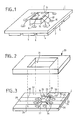
- Figure 1 corresponds to the prior art and has been described in the preamble.
- a memory card 20 which has in its middle a cavity 21 in which must be housed an electronic component, for example the chip 2 in FIG. 1.
- an electronic component for example the chip 2 in FIG. 1.
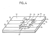
- the support film 1 is replaced by a layer of metal 22, for example copper or nickel, having a thickness of a few tens of microns, for example eighty microns.
- This metal layer 22, deposited on a work support (not shown), is cut along the line which is indicated by the segments 23 to 30 connected to the center by a circular cut 31.
- This cutting can be carried out by any known means and in particular by a chemical process such as etching or a mechanical process using a laser device.
- These different segments 23 to 31 delimit metal zones such as those referenced 32 and 33, which are electrically separated so as to act as contacts. So that these different zones do not separate from each other, a layer 34 of polyimide or silicone is deposited over their entire surface. This deposition is carried out in the liquid phase on the metal and adheres naturally to the latter without modifying the structure of the metal and of the metal zones.
- polyimide or silicone epoxy resin can be used which is deposited at very high temperature. The thickness of this polyimide layer is approximately a few microns, for example three microns. In Figure 3, this polyimide layer is assumed to be transparent.
- the following operation consists in placing and gluing an electronic component 35 on the metal layer 22.
- two solutions are possible: one is to turn the assembly of FIG. 3 so that the polyimide layer 34 is in contact with the working support (FIG. 4), the other is to remove the polyimide layer where the component 35 must be bonded by any known method, for example by chemical attack with mask.
- the mask is provided for removing the polyimide layer, not only at the location of the component 35, but also at the locations 36 where the electrical connections between the component and the metal areas must be made.
- the component 35 is bonded to said area using an adhesive which resists high temperatures.
- This bonding operation of the component 35 is followed by an electrical connection operation of each of the output terminals 37 of the chip 35 to a metal area 32 by means of a conductive wire 38.
- the connection of the ends of each wire conductive can be carried out by any known means, for example by bonding using a conductive adhesive.
- the assembly - polyimide layer 34 and metal layer 22 carrying the electronic component 35 and the electrical connections 38 - is ready to carry out the operation of encapsulation of the electronic component 35 and the electrical connections by any process known, in particular molding in a resin and then heating the assembly to harden the resin and obtain a compact block (not shown). Due to the absence of a support film for the metal layer and of a retaining adhesive between this metal layer and the support film, elements which do not withstand temperatures above 150 ° C, the assembly of each of Figures 3 and 4 can be heated to temperatures in the region of 300 ° C, which considerably accelerates the hardening process of the encapsulation resin. The result is a simpler automatic production line, saving time and money.
- the metal component-layer assembly is put in place on the card 20 (FIG. 2) so that the compact block containing the component 35 and its electrical connections fits into the cavity 21 and that the metal zones come to rest on the edges of the cavity where they are fixed by any known method, in particular by gluing. It will be noted that these metal zones rest directly on the edges of the cavity 21 in the case of FIG. 4 but through the polyimide layer 34 in the case of FIG. 3.
- this layer must be removed to expose the metal areas so that they play their role of electrical contacts .
- This removal can be carried out by any known method, for example by chemical attack without mask, or again by a mechanical method such as polishing.
- This cleaning operation can be carried out before or after the installation of the component-metal layer assembly on the menu. In this cleaning, the underlying polyimide layer 34 should not be damaged.
- the polyimide occupying the spaces between the metal areas is also removed, so that said areas appear in relief on the center of the support 20 and that 'there may be communication holes between the cavity 21 and the environment external to the card.
- the polyimide layer 34 remains in place in the final device. According to a variant of the method, it can be removed before the assembly of the assembly on the card but, in this case, it must be taken into account that the mechanical strength of the metal areas is less good. To remedy this problem, it is proposed to leave the polyimide seals in place between said zones and to replace the polyimide layer with a layer of adhesive which serves to fix the assembly on the card.
Abstract
Description
L'invention concerne un procédé de mise en place d'un composant électronique et de ses connexions électriques sur un support tel qu'une carte d'identification ou une carte bancaire ; elle concerne également le produit obtenu en mettant en oeuvre ce procédé.The invention relates to a method of placing an electronic component and its electrical connections on a support such as an identification card or a bank card; it also relates to the product obtained by implementing this process.
Il est connu d'utiliser des cartes d'identification dans de nombreux domaines notamment dans celui des cartes bancaires ou de crédit. Pendant très longtemps, ces cartes ne comportèrent, outre un numéro d'identification et le nom du titulaire, un enregistrement magnétique qui en permettait l'identification par lecture magnétique. Depuis quelques années, ces cartes sont utilisées à des fonctions autres que l'identification du titulaire et notamment à des fins de pré-payement et de protection contre les actions des fraudeurs. A cet effet, la carte comporte un composant électronique actif qui peut être constitué d'une mémoire électronique associée ou non à un microprocesseur, ce qui permet de l'utiliser notamment pour des applications de type bancaire.It is known to use identification cards in many fields, particularly in that of bank or credit cards. For a very long time, these cards did not include, apart from an identification number and the name of the holder, a magnetic recording which allowed identification by magnetic reading. For a few years, these cards have been used for functions other than identifying the holder and in particular for the purposes of pre-payment and protection against the actions of fraudsters. To this end, the card comprises an active electronic component which can consist of an electronic memory associated or not with a microprocessor, which makes it possible to use it in particular for banking type applications.
Les cartes de l'état de la technique qui comportent un composant électronique sont fabriquées de diverses manières. Dans un premier procédé, une cavité est aménagée dans l'épaisseur de la carte pour recevoir le composant électronique. Dans un autre procédé dit de "co-laminage", on lamine de fines couches de matière plastique : polyépoxy, polyéthylène, polychlorure de vinyl etc... autour du composant. Lors de la mise en oeuvre de ces procédés, diverses opérations sont en outre effectuées pour assurer la connexion électrique des bornes du composant électronique à des métallisations qui sont disposées en surface sur la carte.The prior art cards which include an electronic component are produced in various ways. In a first method, a cavity is arranged in the thickness of the card to receive the electronic component. In another process called "co-lamination", thin layers of plastic are laminated: polyepoxy, polyethylene, polyvinyl chloride, etc. around the component. During the implementation of these methods, various operations are in in addition carried out to ensure the electrical connection of the terminals of the electronic component to metallizations which are arranged on the surface on the card.
L'un des procédés pour mettre en place le composant électronique dans la cavité aménagée dans la carte et pour disposer les métallisations sur la carte ainsi que pour réaliser les connexions entre les bornes de la carte et les métallisations consiste, comme le montre la figure 1, à utiliser un film 1 non conducteur, par exemple en polyépoxy, qui porte, d'un côté, le composant électronique sous forme d'une puce référencée 2 et, de l'autre côté, des surfaces métallisées telles que celles référencées 3, 4 et 5 et séparées les unes des autres par des espaces 6 et 7 sans métallisation. Ces surfaces métallisées 3, 4 et 5 communiquent avec l'autre côté du film 1 par des trous 8, 9 et 10 par l'intermédiaire desquels les extrémités de fils conducteurs 11, 12 et 13 viennent se connecter aux surfaces métallisées correspondantes par tous moyens connus tels qu'une colle conductrice. L'autre extrémité de chaque fil conducteur est connectée à une borne de sortie 14, 15 ou 16 de la puce 2.One of the methods for placing the electronic component in the cavity provided in the card and for placing the metallizations on the card as well as for making the connections between the terminals of the card and the metallizations consists, as shown in FIG. 1 , to use a non-conductive film 1, for example made of polyepoxy, which carries, on the one hand, the electronic component in the form of a chip referenced 2 and, on the other side, metallized surfaces such as those referenced 3, 4 and 5 and separated from each other by
Ces opérations sont ensuite suivies de l'enrobage de la puce 2 avec de la résine et d'une cuisson de la résine pour obtenir l'encapsulation de la puce. On peut alors mettre en place la puce dans la cavité de la carte et disposer les métallisations sur les bords de la cavité par simple emboîtage de la puce et collage du film support 1 sur la carte après son découpage aux dimensions requises.These operations are then followed by coating the
Le procédé qui vient d'être décrit succinctement ci-dessus présente l'inconvénient que le film 1 et la colle qui est utilisée pour maintenir les métallisations 3, 4 et 5 ne peuvent supporter des températures supérieures à 150°C et il en résulte un allongement considérable du temps de cuisson de la résine qui sert à encapsuler la puce 2, ce qui est coûteux, notamment dans une chaîne de fabrication automatique.The process which has just been described succinctly above has the disadvantage that the film 1 and the adhesive which is used to maintain the
Le but de la présente invention est donc de remédier aux inconvénients précités en mettant en oeuvre un procédé de mise en place d'un composant électronique et de ses connexions électriques sur un support qui permet une plus haute température de cuisson de la résine d'enrobage, d'oû un temps de cuisson plus faible et donc un coût moins élevé.The object of the present invention is therefore to remedy the aforementioned drawbacks by implementing a method of placing an electronic component and its electrical connections on a support which allows a higher baking temperature of the coating resin. , hence a shorter cooking time and therefore a lower cost.
L'invention se rapporte à un procédé de mise en place d'un composant électronique et de ses connexions électriques sur un support comportant une cavité pour loger ledit composant, caractérisé en ce qu'il comprend les opération suivantes :
- a) le dépôt sur un support de travail tel qu'une plaquette, d'une couche métallique,
- b) le découpage de cette couche métallique en zones isolées électriquement l'une de l'autre,
- c) le dépôt sur un côté de ces zones métalliques d'une couche de polyimide,
- d) la pose sur un côté de ces zones métalliques du composant électronique comportant des bornes de sortie,
- e) le raccordement électrique des bornes de sortie du composant électronique aux zones métalliques,
- f) l'enrobage du composant électronique par une résine,
- g) le chauffage de l'ensemble à température élevée de manière à obtenir rapidement le durcissement de la résine,
- h) la mise en place de l'ensemble sur le support de manière que le composant électronique encapsulé se loge dans la cavité.
- a) depositing on a working support such as a wafer, a metal layer,
- b) the cutting of this metallic layer into zones electrically isolated from one another,
- c) the deposition on one side of these metal areas of a polyimide layer,
- d) laying on one side of these metal zones of the electronic component comprising output terminals,
- e) the electrical connection of the output terminals of the electronic component to the metal areas,
- f) coating the electronic component with a resin,
- g) heating the assembly to a high temperature so as to rapidly obtain the curing of the resin,
- h) placing the assembly on the support so that the encapsulated electronic component is housed in the cavity.
L'invention se rapporte également à un produit obtenu en mettant en oeuvre le procédé qui comprend une carte support munie d'une cavité et un composant électronique disposé dans ladite cavité, caractérisé en ce que ledit composant électronique est disposé directement sur une couche métallique, qui est collée sur la carte, et que cette couche métallique est divisée en zones correspondant chacune à un contact.The invention also relates to a product obtained by implementing the method which comprises a support card provided with a cavity and an electronic component disposed in said cavity, characterized in that said electronic component is disposed directly on a metal layer, which is stuck on the card, and that this metal layer is divided into zones each corresponding to a contact.
Dans une variante du procédé, le produit obtenu présente un composant électronique qui est fixé sur la couche métallitque par l'intermédiaire d'une couche de polyimide.In a variant of the process, the product obtained has an electronic component which is fixed to the metallitic layer by means of a polyimide layer.
D'autres caractéristiques et avantages de la présente invention apparaîtront à la lecture de la description suivante d'un exemple particulier de réalisation, ladite description étant faite en relation avec le dessin joint dans lequel :
- - la figure 1 est une vue en perspective cavalière d'un film de support de composant électronique et de ses connexions électriques mettant en oeuvre un procédé selon l'invention,
- - la figure 2 est une vue en perspective cavalière d'une carte mémoire prévue pour recevoir un composant électronique,
- - la figure 3 est une vue en perspective cavalière d'un composant électronique disposé sur une couche métallique du support, mettant en oeuvre le procédé selon l'invention, et
- - la figure 4 est une vue en perspective d'un autre mode de réalisation de l'invention.
- FIG. 1 is a perspective view of an electronic component support film and of its electrical connections implementing a method according to the invention,
- FIG. 2 is a perspective view of a memory card intended to receive an electronic component,
- FIG. 3 is a perspective view of an electronic component placed on a metal layer of the support, implementing the method according to the invention, and
- - Figure 4 is a perspective view of another embodiment of the invention.
La figure 1 correspond à l'art antérieur et a été décrite dans le préambule. Sur la figure 2, on a représenté une carte mémoire 20 qui comporte en son milieu une cavité 21 dans laquelle doit venir se loger un composant électronique, par exemple la puce 2 de la figure 1. Dans le procédé de l'art antérieur pour mettre en place la puce dans son logement, il faut bien entendu présenter le film 1 sens dessus-dessous par rapport à la carte 20 de manière que la puce 2 s'emboîte dans la cavité 21.Figure 1 corresponds to the prior art and has been described in the preamble. In Figure 2, there is shown a
Selon l'invention, on remplace le film support 1 par une couche de métal 22, par exemple du cuivre ou du nickel, ayant une épaisseur de quelques dizaines de microns, par exemple quatre-vingt microns. Cette couche métallique 22, déposée sur un support de travail non représenté, est découpée selon le tracé qui est indiqué par les segments 23 à 30 reliés au centre par une découpe circulaire 31. Cette découpe peut être effectuée par tous moyens connus et notamment par un procédé chimique tel que la gravure ou un procédé mécanique mettant en oeuvre un dispositif laser.According to the invention, the support film 1 is replaced by a layer of
Ces différents segments 23 à 31 délimitent des zones métalliques telles que celles référencées 32 et 33, qui sont séparées électriquement de manière à faire office de contacts. Pour que ces différentes zones ne se séparent pas les unes des autres, on dépose sur toute leur surface une couche 34 de polyimide ou de silicone. Ce dépôt est effectué en phase liquide sur le métal et adhère naturellement sur ce dernier sans modifier la structure du métal et des zones métalliques. A la place du polyimide ou de silicone, on peut utiliser de la résine époxy qui est déposée à très haute température. L'épaisseur de cette couche de polyimide est de quelques microns environ, par exemple trois microns. Sur la figure 3, cette couche de polyimide est supposée transparente.These
L'opération suivante consiste à poser et coller un composant électronique 35 sur la couche métallique 22. A cet effet, deux solutions sont possibles : l'une est de retourner l'ensemble de la figure 3 pour que la couche de polyimide 34 soit en contact avec le support de travail (figure 4), l'autre est d'enlever la couche de polyimide à l'endroit où le composant 35 doit être collé par tous procédés connus, par exemple par attaque chimique avec masque. Dans cette deuxième solution, le masque est prévu pour enlever la couche de polyimide, non seulement à l'endroit du composant 35, mais aussi aux endroits 36 où les connexions électriques entre le composant et les zones métalliques doivent être effectuées. Lorsque la zone du composant a été dégagée dans la couche de polyimide, le composant 35 est collé sur ladite zone à l'aide d'une colle qui résiste aux hautes températures.The following operation consists in placing and gluing an
Cette opération de collage du composant 35 est suivie d'une opération de raccordement électrique de chacune des bornes de sortie 37 de la puce 35 à une zone métallique 32 par l'intermédiaire d'un fil conducteur 38. Le raccordement des extrémités de chaque fil conducteur peut être effectué par tous moyens connus, par exemple par collage à l'aide d'une colle conductrice.This bonding operation of the
A ce stade du procédé, l'ensemble -couche de polyimide 34 et couche métallique 22 portant le composant électronique 35 et les connexions électriques 38- est prêt pour effectuer l'opération d'encapsulation du composant électronique 35 et des connexions électriques par tous procédés connus, notamment le moulage dans une résine puis chauffage de l'ensemble pour durcir la résine et obtenir un bloc compact (non représenté). Du fait de l'absence d'un film support de la couche métallique et d'une colle de maintien entre cette couche métallique et le film support, éléments qui ne résistent pas à des températures supérieures à 150°C, l'ensemble de chacune des figures 3 et 4 peut être chauffé à des températures voisines de 300°C, ce qui accélère considérablement le processus de durcissement de la résine d'encapsulation. Il en résulte une chaîne de fabrication automatique plus simple et un gain de temps et d'argent.At this stage of the process, the assembly - polyimide layer 34 and
Lorsque l'opération d'encapsulation est terminée, l'ensemble composant-couche métallique est mis en place sur la carte 20 (figure 2) de manière que le bloc compact contenant le composant 35 et ses connexions électriques s'emboîte dans la cavité 21 et que les zones métalliques viennent reposer sur les bords de la cavité où ils sont fixés par tous procédés connus, notamment par collage. On remarquera que ces zones métalliques reposent directement sur les bords de la cavité 21 dans le cas de la figure 4 mais par l'intermédiaire de la couche de polyimide 34 dans le cas de la figure 3.When the encapsulation operation is finished, the metal component-layer assembly is put in place on the card 20 (FIG. 2) so that the compact block containing the
Dans le cas de la figure 4, comme la couche de polyimide 34 rencontre le côté extérieur des zones métalliques après mise en place sur la carte, cette couche doit être enlevée pour dégager les zones métalliques de manière qu'elles jouent leur rôle de contacts électriques. Cet enlèvement peut être effectué par tous procédés connus, par exemple par attaque chimique sans masque, soit encore par un procédé mécanique tel que le polissage.In the case of FIG. 4, as the polyimide layer 34 meets the outer side of the metal areas after being placed on the card, this layer must be removed to expose the metal areas so that they play their role of electrical contacts . This removal can be carried out by any known method, for example by chemical attack without mask, or again by a mechanical method such as polishing.
Dans le cas de la figure 3, il est également prévu d'enlever les bavures de polyimide qui peuvent s'être formées sur le côté des zones métalliques opposé à celui de la couche de polyimide. Cette opération de nettoyage peut être effectuée avant ou après la mise en place de l'ensemble composant-couche métallique sur la carte. Dans ce nettoyage, il convient de ne pas abîmer la couche de polyimide sous-jacente 34.In the case of FIG. 3, provision is also made to remove the polyimide burrs which may have formed on the side of the metal zones opposite to that of the polyimide layer. This cleaning operation can be carried out before or after the installation of the component-metal layer assembly on the menu. In this cleaning, the underlying polyimide layer 34 should not be damaged.
Lors de cette opération d'enlèvement de la couche de polyimide ou de ses bavures sur le côté opposé, le polyimide occupant les espaces entre les zones métalliques est également retiré, de sorte que lesdites zones apparaissent en relief sur le centre du support 20 et qu'il peut exister des trous de communication entre la cavité 21 et l'environnement extérieur à la carte. Pour éviter ces trous, il est prévu que l'encapsulation conduise à une capsule de dimensions aussi proches que possible de celles de la cavité. Il peut également être prévu de laisser en place le polyimide entre les zones métalliques, ce qui signifie qu'il ne faut pas utiliser une attaque chimique pour l'enlèvement du polyimide mais un polissage mécanique.During this operation of removing the polyimide layer or its burrs on the opposite side, the polyimide occupying the spaces between the metal areas is also removed, so that said areas appear in relief on the center of the
Dans le cas du procédé correspondant à la figure 3, la couche de polyimide 34 reste en place dans le dispositif final. Selon une variante du procédé, elle peut être enlevée avant la mise en place de l'ensemble sur la carte mais, dans ce cas, il faut tenir compte que la tenue mécanique des zones métalliques est moins bonne. Pour remédier à ce problème, il est proposé de laisser en place les joints de polyimide entre lesdites zones et de remplacer la couche de polyimide par une couche de colle qui sert à fixer l'ensemble sur la carte.In the case of the method corresponding to FIG. 3, the polyimide layer 34 remains in place in the final device. According to a variant of the method, it can be removed before the assembly of the assembly on the card but, in this case, it must be taken into account that the mechanical strength of the metal areas is less good. To remedy this problem, it is proposed to leave the polyimide seals in place between said zones and to replace the polyimide layer with a layer of adhesive which serves to fix the assembly on the card.
Claims (9)
Applications Claiming Priority (2)
| Application Number | Priority Date | Filing Date | Title |
|---|---|---|---|
| FR8717386 | 1987-12-14 | ||
| FR8717386A FR2624651B1 (en) | 1987-12-14 | 1987-12-14 | METHOD FOR SETTING UP AN ELECTRONIC COMPONENT AND ITS ELECTRICAL CONNECTIONS ON A SUPPORT AND PRODUCT THUS OBTAINED |
Publications (2)
| Publication Number | Publication Date |
|---|---|
| EP0321327A1 true EP0321327A1 (en) | 1989-06-21 |
| EP0321327B1 EP0321327B1 (en) | 1996-04-10 |
Family
ID=9357823
Family Applications (1)
| Application Number | Title | Priority Date | Filing Date |
|---|---|---|---|
| EP88403140A Expired - Lifetime EP0321327B1 (en) | 1987-12-14 | 1988-12-09 | Method of mounting an electronic component and its electronic connections on a support |
Country Status (6)
| Country | Link |
|---|---|
| US (1) | US4908937A (en) |
| EP (1) | EP0321327B1 (en) |
| JP (1) | JP2761501B2 (en) |
| KR (1) | KR890010748A (en) |
| DE (1) | DE3855197T2 (en) |
| FR (1) | FR2624651B1 (en) |
Cited By (2)
| Publication number | Priority date | Publication date | Assignee | Title |
|---|---|---|---|---|
| DE4224103A1 (en) * | 1992-07-22 | 1994-01-27 | Manfred Dr Ing Michalk | Miniature housing with electronic components |
| WO1997044823A1 (en) * | 1996-05-17 | 1997-11-27 | Siemens Aktiengesellschaft | Substrate for a semiconductor chip |
Families Citing this family (10)
| Publication number | Priority date | Publication date | Assignee | Title |
|---|---|---|---|---|
| FR2664721B1 (en) * | 1990-07-10 | 1992-09-25 | Gemplus Card Int | REINFORCED CHIP CARD. |
| FR2695234B1 (en) * | 1992-08-26 | 1994-11-04 | Gemplus Card Int | Method of marking a smart card. |
| US5581445A (en) * | 1994-02-14 | 1996-12-03 | Us3, Inc. | Plastic integrated circuit card with reinforcement structure for protecting integrated circuit module |
| FR2724477B1 (en) * | 1994-09-13 | 1997-01-10 | Gemplus Card Int | NON-CONTACT CARD MANUFACTURING PROCESS |
| FR2777675B1 (en) | 1998-04-15 | 2001-12-07 | Rue Cartes Et Systemes De | METHOD OF MANUFACTURING A MICROCIRCUIT CARD AND A MICROCIRCUIT CARD OBTAINED BY IMPLEMENTATION OF THIS PROCESS |
| JP4749656B2 (en) | 2001-02-09 | 2011-08-17 | 台湾積體電路製造股▲ふん▼有限公司 | Manufacturing method of semiconductor device and semiconductor device obtained by this method |
| DE10217262A1 (en) * | 2002-04-18 | 2003-11-06 | Pall Corp | Filter module and method for producing a filled filter module |
| JP5011726B2 (en) | 2003-08-01 | 2012-08-29 | 旭硝子株式会社 | Coating material for solar thermal power generation system and solar thermal power generation system extending the same |
| US20060175711A1 (en) * | 2005-02-08 | 2006-08-10 | Hannstar Display Corporation | Structure and method for bonding an IC chip |
| DE102007019795B4 (en) * | 2007-04-26 | 2012-10-04 | Infineon Technologies Ag | Chip module and method for manufacturing this chip module |
Citations (1)
| Publication number | Priority date | Publication date | Assignee | Title |
|---|---|---|---|---|
| EP0128822A1 (en) * | 1983-06-09 | 1984-12-19 | Flonic S.A. | Method of producing memory cards, and cards obtained thereby |
Family Cites Families (5)
| Publication number | Priority date | Publication date | Assignee | Title |
|---|---|---|---|---|
| DE3248385A1 (en) * | 1982-12-28 | 1984-06-28 | GAO Gesellschaft für Automation und Organisation mbH, 8000 München | ID CARD WITH INTEGRATED CIRCUIT |
| WO1985002060A1 (en) * | 1983-10-24 | 1985-05-09 | Sintra-Alcatel, S.A. | Method for substituting an electronic component connected to the conductor tracks of a carrier substrate |
| JPS6095941A (en) * | 1983-10-31 | 1985-05-29 | Toshiba Corp | Semiconductor device |
| JPS6115289A (en) * | 1984-06-29 | 1986-01-23 | Mitsubishi Plastics Ind Ltd | Memory card |
| US4801765A (en) * | 1986-01-06 | 1989-01-31 | American Telephone And Telegraph Company, At&T Bell Laboratories | Electronic component package using multi-level lead frames |
-
1987
- 1987-12-14 FR FR8717386A patent/FR2624651B1/en not_active Expired - Lifetime
-
1988
- 1988-12-09 DE DE3855197T patent/DE3855197T2/en not_active Expired - Fee Related
- 1988-12-09 EP EP88403140A patent/EP0321327B1/en not_active Expired - Lifetime
- 1988-12-12 KR KR1019880016607A patent/KR890010748A/en not_active Application Discontinuation
- 1988-12-12 US US07/283,214 patent/US4908937A/en not_active Ceased
- 1988-12-14 JP JP63316074A patent/JP2761501B2/en not_active Expired - Lifetime
Patent Citations (1)
| Publication number | Priority date | Publication date | Assignee | Title |
|---|---|---|---|---|
| EP0128822A1 (en) * | 1983-06-09 | 1984-12-19 | Flonic S.A. | Method of producing memory cards, and cards obtained thereby |
Non-Patent Citations (1)
| Title |
|---|
| PATENT ABSTRACTS OF JAPAN * |
Cited By (2)
| Publication number | Priority date | Publication date | Assignee | Title |
|---|---|---|---|---|
| DE4224103A1 (en) * | 1992-07-22 | 1994-01-27 | Manfred Dr Ing Michalk | Miniature housing with electronic components |
| WO1997044823A1 (en) * | 1996-05-17 | 1997-11-27 | Siemens Aktiengesellschaft | Substrate for a semiconductor chip |
Also Published As
| Publication number | Publication date |
|---|---|
| JPH021399A (en) | 1990-01-05 |
| US4908937A (en) | 1990-03-20 |
| FR2624651A1 (en) | 1989-06-16 |
| DE3855197D1 (en) | 1996-05-15 |
| DE3855197T2 (en) | 1996-10-02 |
| JP2761501B2 (en) | 1998-06-04 |
| KR890010748A (en) | 1989-08-10 |
| FR2624651B1 (en) | 1991-09-06 |
| EP0321327B1 (en) | 1996-04-10 |
Similar Documents
| Publication | Publication Date | Title |
|---|---|---|
| EP0391790B1 (en) | Method of manufacturing an electronic module | |
| EP0128822B1 (en) | Method of producing memory cards, and cards obtained thereby | |
| EP0321340B1 (en) | Electronic-component support, especially for a memory card, and product so obtained | |
| EP0297991B1 (en) | Method of fabricating an electronic microcircuit card | |
| EP0197438B1 (en) | Method of manufacturing electronic modules for microcircuit boards and modules obtained by this method | |
| EP0207853B1 (en) | Method for mounting an integrated circuit on a support, resultant device and its use in an electronic microcircuit card | |
| FR2488446A1 (en) | SUPPORT ELEMENT FOR AN INTEGRATED CIRCUIT MODULE | |
| EP0321327B1 (en) | Method of mounting an electronic component and its electronic connections on a support | |
| EP0094716A1 (en) | Process for connecting a semiconductor to elements of a support, particularly of a portable card | |
| EP0490739A1 (en) | Interconnection method and device for three-dimensional integrated circuits | |
| FR2857157A1 (en) | METHOD FOR INTERCONNECTING ACTIVE AND PASSIVE COMPONENTS AND HETEROGENEOUS COMPONENT WITH LOW THICKNESS THEREFROM | |
| FR2769441A1 (en) | CONTACTLESS ELECTRONIC CARD AND MANUFACTURING METHOD THEREOF | |
| EP0321326B1 (en) | Method for positioning an electronic component on a substrate | |
| FR2784210A1 (en) | CONTACTLESS CHIP CARD COMPRISING MEANS OF INHIBITION | |
| FR2618254A1 (en) | METHOD AND STRUCTURE FOR TAKING CONTACT ON INTEGRATED CIRCUIT PLOTS. | |
| EP0323295B1 (en) | Method for fixing an electronic component and its contacts on a carrier | |
| FR2828570A1 (en) | Production of a contact-less chip support comprises laminating an insulating film on a micro-module film, laminating an adhesive film on the micro-module film, cutting the micro-module and applying an antenna to each micro-module | |
| WO2000031686A1 (en) | Method for making a flush chip card using a laser engraving step and resulting chip card | |
| EP1192593A1 (en) | Device and method for making devices comprising at least a chip mounted on a support | |
| FR2777675A1 (en) | METHOD FOR MANUFACTURING A MICROCIRCUIT CARD AND A MICROCIRCUIT CARD OBTAINED BY IMPLEMENTATION OF THIS PROCESS | |
| FR2817656A1 (en) | ELECTRICAL INSULATION OF GROUPED MICROCIRCUITS BEFORE UNIT BONDING | |
| EP1709574A1 (en) | Method for manufacturing an electronic key with usb connector and electronic key obtained | |
| WO2000077727A1 (en) | Module comprising at least a chip and its communication interface, object comprising a module and method for making said modules | |
| WO2000079478A1 (en) | Method for making a module for chip cards and resulting module | |
| EP1210690A1 (en) | Electronic device comprising a chip fixed on a support and method for making same |
Legal Events
| Date | Code | Title | Description |
|---|---|---|---|
| PUAI | Public reference made under article 153(3) epc to a published international application that has entered the european phase |
Free format text: ORIGINAL CODE: 0009012 |
|
| AK | Designated contracting states |
Kind code of ref document: A1 Designated state(s): DE ES GB IT NL |
|
| 17P | Request for examination filed |
Effective date: 19890725 |
|
| 17Q | First examination report despatched |
Effective date: 19920331 |
|
| GRAA | (expected) grant |
Free format text: ORIGINAL CODE: 0009210 |
|
| AK | Designated contracting states |
Kind code of ref document: B1 Designated state(s): DE ES GB IT NL |
|
| PG25 | Lapsed in a contracting state [announced via postgrant information from national office to epo] |
Ref country code: NL Free format text: LAPSE BECAUSE OF FAILURE TO SUBMIT A TRANSLATION OF THE DESCRIPTION OR TO PAY THE FEE WITHIN THE PRESCRIBED TIME-LIMIT Effective date: 19960410 |
|
| REF | Corresponds to: |
Ref document number: 3855197 Country of ref document: DE Date of ref document: 19960515 |
|
| ITF | It: translation for a ep patent filed |
Owner name: PORTA CHECCACCI E BOTTI S.R.L. |
|
| GBT | Gb: translation of ep patent filed (gb section 77(6)(a)/1977) |
Effective date: 19960507 |
|
| PG25 | Lapsed in a contracting state [announced via postgrant information from national office to epo] |
Ref country code: ES Free format text: LAPSE BECAUSE OF FAILURE TO SUBMIT A TRANSLATION OF THE DESCRIPTION OR TO PAY THE FEE WITHIN THE PRESCRIBED TIME-LIMIT Effective date: 19960721 |
|
| NLV1 | Nl: lapsed or annulled due to failure to fulfill the requirements of art. 29p and 29m of the patents act | ||
| PGFP | Annual fee paid to national office [announced via postgrant information from national office to epo] |
Ref country code: ES Payment date: 19961228 Year of fee payment: 9 |
|
| PLBE | No opposition filed within time limit |
Free format text: ORIGINAL CODE: 0009261 |
|
| STAA | Information on the status of an ep patent application or granted ep patent |
Free format text: STATUS: NO OPPOSITION FILED WITHIN TIME LIMIT |
|
| 26N | No opposition filed | ||
| REG | Reference to a national code |
Ref country code: GB Ref legal event code: IF02 |
|
| PGFP | Annual fee paid to national office [announced via postgrant information from national office to epo] |
Ref country code: GB Payment date: 20021204 Year of fee payment: 15 |
|
| PGFP | Annual fee paid to national office [announced via postgrant information from national office to epo] |
Ref country code: DE Payment date: 20021212 Year of fee payment: 15 |
|
| PG25 | Lapsed in a contracting state [announced via postgrant information from national office to epo] |
Ref country code: GB Free format text: LAPSE BECAUSE OF NON-PAYMENT OF DUE FEES Effective date: 20031209 |
|
| PG25 | Lapsed in a contracting state [announced via postgrant information from national office to epo] |
Ref country code: DE Free format text: LAPSE BECAUSE OF NON-PAYMENT OF DUE FEES Effective date: 20040701 |
|
| GBPC | Gb: european patent ceased through non-payment of renewal fee |
Effective date: 20031209 |
|
| PG25 | Lapsed in a contracting state [announced via postgrant information from national office to epo] |
Ref country code: IT Free format text: LAPSE BECAUSE OF NON-PAYMENT OF DUE FEES;WARNING: LAPSES OF ITALIAN PATENTS WITH EFFECTIVE DATE BEFORE 2007 MAY HAVE OCCURRED AT ANY TIME BEFORE 2007. THE CORRECT EFFECTIVE DATE MAY BE DIFFERENT FROM THE ONE RECORDED. Effective date: 20051209 |