EP0254960B1 - A multiprocessor system - Google Patents
A multiprocessor system Download PDFInfo
- Publication number
- EP0254960B1 EP0254960B1 EP87110224A EP87110224A EP0254960B1 EP 0254960 B1 EP0254960 B1 EP 0254960B1 EP 87110224 A EP87110224 A EP 87110224A EP 87110224 A EP87110224 A EP 87110224A EP 0254960 B1 EP0254960 B1 EP 0254960B1
- Authority
- EP
- European Patent Office
- Prior art keywords
- processor
- group
- memory
- sync
- lock
- Prior art date
- Legal status (The legal status is an assumption and is not a legal conclusion. Google has not performed a legal analysis and makes no representation as to the accuracy of the status listed.)
- Expired - Lifetime
Links
- 230000015654 memory Effects 0.000 claims description 73
- 238000004891 communication Methods 0.000 claims description 15
- 230000003111 delayed effect Effects 0.000 claims description 2
- 230000002401 inhibitory effect Effects 0.000 claims 2
- 230000000063 preceeding effect Effects 0.000 claims 1
- 238000000034 method Methods 0.000 description 6
- 238000012546 transfer Methods 0.000 description 5
- 230000006870 function Effects 0.000 description 3
- 238000012545 processing Methods 0.000 description 2
- 230000005540 biological transmission Effects 0.000 description 1
- 238000012217 deletion Methods 0.000 description 1
- 230000037430 deletion Effects 0.000 description 1
- 238000010586 diagram Methods 0.000 description 1
- 238000011156 evaluation Methods 0.000 description 1
- 238000004088 simulation Methods 0.000 description 1
- 230000001360 synchronised effect Effects 0.000 description 1
- 238000012360 testing method Methods 0.000 description 1
Images


Classifications
-
- G—PHYSICS
- G06—COMPUTING; CALCULATING OR COUNTING
- G06F—ELECTRIC DIGITAL DATA PROCESSING
- G06F9/00—Arrangements for program control, e.g. control units
- G06F9/06—Arrangements for program control, e.g. control units using stored programs, i.e. using an internal store of processing equipment to receive or retain programs
- G06F9/46—Multiprogramming arrangements
- G06F9/52—Program synchronisation; Mutual exclusion, e.g. by means of semaphores
-
- G—PHYSICS
- G06—COMPUTING; CALCULATING OR COUNTING
- G06F—ELECTRIC DIGITAL DATA PROCESSING
- G06F15/00—Digital computers in general; Data processing equipment in general
- G06F15/16—Combinations of two or more digital computers each having at least an arithmetic unit, a program unit and a register, e.g. for a simultaneous processing of several programs
- G06F15/163—Interprocessor communication
- G06F15/17—Interprocessor communication using an input/output type connection, e.g. channel, I/O port
-
- G—PHYSICS
- G06—COMPUTING; CALCULATING OR COUNTING
- G06F—ELECTRIC DIGITAL DATA PROCESSING
- G06F15/00—Digital computers in general; Data processing equipment in general
- G06F15/16—Combinations of two or more digital computers each having at least an arithmetic unit, a program unit and a register, e.g. for a simultaneous processing of several programs
- G06F15/163—Interprocessor communication
- G06F15/173—Interprocessor communication using an interconnection network, e.g. matrix, shuffle, pyramid, star, snowflake
- G06F15/17337—Direct connection machines, e.g. completely connected computers, point to point communication networks
Definitions
- This invention relates to a communication scheme between processors in a multiprocessor computer architecture. More particularly, this invention relates to an improvement of accessing a shared memory which is located in each processor group and is used for inter-processor data transmission.
- the present invention relates to the one having a shared memory located in each processor group exclusively for transferring the data as shown in FIG. 1.
- the processors in operation are required that a data transfer between the processors must be synchronized with a data processing therein.
- synchronize or "synchronization” is hereinafter used to mean an adjustment of timing to start and stop the tasks which competes with each other. Therefore, in the multiprocessor system, an easy means for fast operation of this synchronization has been necessarily requested.
- FIG. 2 A method of processor synchronization employed in the prior art system by a software control is shown in FIG. 2.
- a processor PA having its local memory LMA i.e. a memory which is directly accessed from its processor, and another processor PB having its local memory LMB are interconnected with each other by a communication network 3, as communication means, thus composing a multiprocessor system.
- the communication network 3 may be a bus or another network, such as a local-area network or a telephone line.
- the second processor PB For the second processor PB to read or write the memory LMA of the first processor PA, the second processor PB must check the status of the local memory LMA by the flags through the communication network 3 by the use of a predetermined protocol.
- FIG. 3 A second method of the processor synchronization employed in the prior art system achieved by a hardware control is shown in FIG. 3.
- processors PA and PB each having the local memory have a control line 4 between two processors, and has a communication means 5 and 5′ directly connected from a processor to the other processor's local memory.
- Each of the communication means 5 and 5′ includes a data bus 52 and a control line 51 for the access control.
- the line 4 is used exclusively for synchronization control. In this system, the load of the software as well as the overhead operation of the system is light. However, the line 4 for synchronization must be installed between all the processors to form a complete graph as shown in FIG. 4, where, as an example, five processors P1 through P5 are included.
- the required quantity of the control lines 4 for the system is n(n-1), where n indicates number of the processors. Therefore, the problem is that the hardware structure of the system becomes too much complicated to be applied to a large scale multiprocessor system.
- a third method of the processor synchronization is carried out by a hardware or a combination of a hardware and a sofware, as reported in "Multiprocessor Cache Synchronization" by Philip Bitar et al on IEEE International Symposium on Computer Architecture l986.
- Multiprocessor Cache Synchronization by Philip Bitar et al on IEEE International Symposium on Computer Architecture l986.
- a set of flag bits i.e. a LOCK bit and SYNC bit
- a control circuit for controlling accesses to a local memory are provided to each processor group.
- the LOCK bit is in a SET state
- a reading-out of the local memory in the first processor group from the second processor is inhibitted while the first processor is writing into the local memory.
- the SYNC bit in a RESET state accepts a read request to the local memory from the second processor after the first processor finishes writing into the local memory, as well as inhibits writing into the local memory from the first processor.
- the setting of the LOCK bit as well as the resetting of the SYNC bit can be carried out within each group without using the network communication.
- the setting of the SYNC bit is carried out implicitly by the memory access, in other words, it does not require a network communication.
- the software is free from the job for synchronization, and the network for the synchronization control is replaced by the access control lines.
- a reduced network traffic or a less sophisticated network is accomplished owing to the deletion of the synchronization control via the network, resulting in a high speed processor operation as well as a high performance capability of the network.
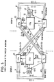
- FIG. 1 shows a general concept of a multiprocessor system using a memory for data transfer.
- FIG. 2 shows schematic configuration of a prior art multiprocessor system where the synchronization is controlled by software.
- FIG. 3 shows schematic configuration of a prior art multiprocessor system where the synchronization is controlled by hardware with an additional software for synchronization control.
- FIG. 4 shows required networks in the configuration of FIG. 3.
- FIG. 5 shows schematic configuration of a multiprocessor system according to the present invention.
- FIG. 6 shows the control circuit in detail used for the present invention.
- FIG. 7 shows a truth table of the flags of the present invention.
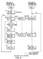
- FIG. 8 shows flow charts for explaining the operation of the present invention.
- FIG. 9 shows a truth table corresponding the flow shown in FIG. 8.
- FIG. 5 An embodiment of the present invention is hereinafter described referring to a principle block diagram of FIG. 5, where the multiprocessor system is composed of two processors 11 (PA) and 12 (PB) shown as representatives of a plurality of processors.
- Each processor PA and PB has own local memory LMA and LMB respectively.
- the term “own” is used to mean “belonging to the same group", i.e. in other words “accessable without using a network”.
- a term “other” is hereinafter used to mean the contrary meaning of the "own”.
- the memory LMA of the group A is accessed from the own processor PA and also from the processor PB of the other group B, thus the memory is shared by the two processors.
- a control circuit 31 having a set (41) of flag bits, one named a LOCK bit another one named a SYNC bit, are provided in the group A, for controlling the transfer of an access request from the processor PA or PB to the memory LMA.
- CTLA control circuit 31
- a second control circuit 32 having a set of flag bits (42) is provided in the group B, for controlling the transfer of an access request from the processor PA or PB to the memory LMB. Function of the control circuits and the flag bits shall be described in detail later on.
- Communication means 6 between the processors PA (or PB) and each own local memory LMA (or LMB) are composed of: data buses 11-21D, 12-22D, for each processor PA, PB to write a data into each own memory LMA, LMB; and access control lines 21-11C, 22-12C, each for delivering an acknowledge signal ACK to each request source PA, PB.
- Communication means 7 between the processor PA (or PB) and the memories LMB (or LMA) of their respectively opposite groups are composed of: data buses 21-12D, 22-11D, for each processor PB, PA to read a data out of their respectively opposite group's memory LMA, LMB; access control lines 21-12C, 22-11C, each for delivering an acknowledge signal ACK to each request source PB, PA; and access control lines 11-32C, 12-31C, each for delivering a read request signal "Read REQ" from each other processor PB, PA to each own control circuit CTLA, CTLB.
- control circuit 31 or 32 CTLA or CTLB
- flag bits 41 or 42
- FIG. 6 A typical structure of the control circuit 31 or 32 (CTLA or CTLB) and the flag bits 41 (or 42) are shown in FIG. 6, and its truth table is shown in FIG. 7, where a positive logic is employed.
- the control circuit CTLA 31 (or CTLB 32) is composed of AND gates 3a, 3b, 3c and a delay circuit 3d.
- the flag bit 41 is composed of widely used memory devices, such as flip-flops, one, 41-1, for the LOCK bit and one, 41-2, for the SYNC bit.
- the AND gate 3a is gated by the LOCK bit as well as the SYNC bit.
- One of the input terminals of the AND gate 3c is gated by the read request signal "Read REQ” from other processor 12 (PB), because the data transfer is from the own processor 11 (PA) to the other processor 12 (PB).
- One of the input terminals of the AND gate 3b is gated by the write request signal "Write REQ” from the own processor 11 (PA).
- the delay circuit 3d formed of widely used delay device to produce a predetermined delay time, which is equivalent to the time required for finishing reading a data to be transferred by a single operation. Accordingly, the SYNC bit 41-2 is automatically set as soon as the reading is finished.
- the control circuit CTLA and the flag bits operate as shown in the truth table of FIG. 7, where "Y" indicates that the request is permitted and "N" indicates that the request is inhibitted.
- the A group includes the processors 11 (PA), the memory 21 (LMA), the circuit control and 31 (CTLA) and its flag bits 41
- the B group includes the processors 12 (PB), the memory 22 (LMB), the control circuit 32 (CTLB) and its flag bits 42, as described below and shown in FIG. 8.
- the numerals for the procedure steps are also cited in the flow charts of FIG. 8. Dotted lines in FIG. 8 show "flows" of the flag information.
- the local memory LMA is written in exclusively by the own processor PA as well as readed out exclusively by the processor PB of the other group B, it is apparently possible for the reverse case where the local memory LMB is readed out by the own processor PA as well as written in by the processor PB of its own group B.
- each group may be provided with a plurality of the sets of flag bits, wherein each set communicates with a corresponding one of a plurality of the processors.
- control circuit 31 of FIG. 6 is referred to as a typical sample, any other circuit configuration which achieves the above-described function can be used in place of the circuit shown in FIG. 6.
- the software can be perfectly free from the job for synchronization, because the processor can be waited by inhibitting the access request signal, resulting in a reduced network traffic, that is, a high-speed operation, and
Landscapes
- Engineering & Computer Science (AREA)
- Theoretical Computer Science (AREA)
- Computer Hardware Design (AREA)
- Software Systems (AREA)
- Physics & Mathematics (AREA)
- General Engineering & Computer Science (AREA)
- General Physics & Mathematics (AREA)
- Mathematical Physics (AREA)
- Multi Processors (AREA)
Description
- This invention relates to a communication scheme between processors in a multiprocessor computer architecture. More particularly, this invention relates to an improvement of accessing a shared memory which is located in each processor group and is used for inter-processor data transmission.
- In the past several years, a multiprocessor system has been intensively employed, where a plurality of processors are provided, with which a data processing is carried out concurrently in parallel so that a high-speed operation a single processor never achieve can be realized. Among several types of the multiprocessor systems, the present invention relates to the one having a shared memory located in each processor group exclusively for transferring the data as shown in FIG. 1. In order to achieve the high-speed operation, the processors in operation are required that a data transfer between the processors must be synchronized with a data processing therein. The above-referred term "synchronize" or "synchronization" is hereinafter used to mean an adjustment of timing to start and stop the tasks which competes with each other. Therefore, in the multiprocessor system, an easy means for fast operation of this synchronization has been necessarily requested.
- A method of processor synchronization employed in the prior art system by a software control is shown in FIG. 2. A processor PA having its local memory LMA, i.e. a memory which is directly accessed from its processor, and another processor PB having its local memory LMB are interconnected with each other by a
communication network 3, as communication means, thus composing a multiprocessor system. Thecommunication network 3 may be a bus or another network, such as a local-area network or a telephone line. For the second processor PB to read or write the memory LMA of the first processor PA, the second processor PB must check the status of the local memory LMA by the flags through thecommunication network 3 by the use of a predetermined protocol. In other words, some particular bits, the so-called semaphore flags, are provided on the memory, and the synchronization is carried out by the so-called "Test and Set" command using the semaphore flags. Problems of this method are: 1) the software for the synchronization is very complex as well as requires much of the overhead operation, i.e. an operation required for indirect jobs, though the hardware is simpler than the below-described second method, and 2) the communication for the synchronization control via the network causes an increase of the network traffic. Accordingly, efficiency of the network throughput is deteriorated, or the network is required to be of a higher performance capability. - A second method of the processor synchronization employed in the prior art system achieved by a hardware control is shown in FIG. 3. Similarly to the configuration of FIG. 2, processors PA and PB each having the local memory have a
control line 4 between two processors, and has a communication means 5 and 5′ directly connected from a processor to the other processor's local memory. Each of the communication means 5 and 5′ includes a data bus 52 and a control line 51 for the access control. Theline 4 is used exclusively for synchronization control. In this system, the load of the software as well as the overhead operation of the system is light. However, theline 4 for synchronization must be installed between all the processors to form a complete graph as shown in FIG. 4, where, as an example, five processors P1 through P5 are included. The required quantity of thecontrol lines 4 for the system is n(n-1), where n indicates number of the processors. Therefore, the problem is that the hardware structure of the system becomes too much complicated to be applied to a large scale multiprocessor system. - A third method of the processor synchronization is carried out by a hardware or a combination of a hardware and a sofware, as reported in "Multiprocessor Cache Synchronization" by Philip Bitar et al on IEEE International Symposium on Computer Architecture l986. However, there are still same problems as those of the software control.
- The latest trends of the multiprocessor synchronization system are also reported in papers: "A Class of Compatible Cache Consistency Protocols and their Support by the IEEE Futurebus" by Paul Sweazey et al on the same issue, and "Cache Coherence Protocols: Evaluation Using Multiprocessor Simulation Model" by James Archibald et al on ACM (Association for Computing Machinary) Transaction on Computer Systems, vol. 4, No. 4, Nov. 1986.
- It is a general object of the invention, therefore to provide a multiprocessor system having a simple hardware configuration as well as having no load of the software for the processor synchronization, and achieving a high speed processor operation and a high performance capability of the network.
- According to the multiprocessor system of the invention, a set of flag bits, i.e. a LOCK bit and SYNC bit, and a control circuit for controlling accesses to a local memory are provided to each processor group. When the LOCK bit is in a SET state, a reading-out of the local memory in the first processor group from the second processor is inhibitted while the first processor is writing into the local memory. The SYNC bit in a RESET state accepts a read request to the local memory from the second processor after the first processor finishes writing into the local memory, as well as inhibits writing into the local memory from the first processor. Accordingly, the setting of the LOCK bit as well as the resetting of the SYNC bit can be carried out within each group without using the network communication. And, the setting of the SYNC bit is carried out implicitly by the memory access, in other words, it does not require a network communication.
- Therefore, the software is free from the job for synchronization, and the network for the synchronization control is replaced by the access control lines. Thus, a reduced network traffic or a less sophisticated network is accomplished owing to the deletion of the synchronization control via the network, resulting in a high speed processor operation as well as a high performance capability of the network.
- The above-mentioned features and advantages of the present invention, together with other objects and advantages, which will become apparent, will be more fully described hereinafter, reference being made to the accompanying drawings forming a part hereof, wherein like numerals refer to like parts throughout. The invention and its embodiments are explained more fully in the following detailed description with reference to the drawings, in which:
- FIG. 1 shows a general concept of a multiprocessor system using a memory for data transfer.
- FIG. 2 shows schematic configuration of a prior art multiprocessor system where the synchronization is controlled by software.
- FIG. 3 shows schematic configuration of a prior art multiprocessor system where the synchronization is controlled by hardware with an additional software for synchronization control.
- FIG. 4 shows required networks in the configuration of FIG. 3.
- FIG. 5 shows schematic configuration of a multiprocessor system according to the present invention.
- FIG. 6 shows the control circuit in detail used for the present invention.
- FIG. 7 shows a truth table of the flags of the present invention.
- FIG. 8 shows flow charts for explaining the operation of the present invention.
- FIG. 9 shows a truth table corresponding the flow shown in FIG. 8.
- An embodiment of the present invention is hereinafter described referring to a principle block diagram of FIG. 5, where the multiprocessor system is composed of two processors 11 (PA) and 12 (PB) shown as representatives of a plurality of processors. Each processor PA and PB has own local memory LMA and LMB respectively. The term "own" is used to mean "belonging to the same group", i.e. in other words "accessable without using a network". A term "other" is hereinafter used to mean the contrary meaning of the "own". The memory LMA of the group A is accessed from the own processor PA and also from the processor PB of the other group B, thus the memory is shared by the two processors. A control circuit 31 (CTLA) having a set (41) of flag bits, one named a LOCK bit another one named a SYNC bit, are provided in the group A, for controlling the transfer of an access request from the processor PA or PB to the memory LMA. Symmetrically similar to the control circuit CTLA, a second control circuit 32 (CTLB) having a set of flag bits (42) is provided in the group B, for controlling the transfer of an access request from the processor PA or PB to the memory LMB. Function of the control circuits and the flag bits shall be described in detail later on.
- Communication means 6 (or 6′) between the processors PA (or PB) and each own local memory LMA (or LMB) are composed of: data buses 11-21D, 12-22D, for each processor PA, PB to write a data into each own memory LMA, LMB; and access control lines 21-11C, 22-12C, each for delivering an acknowledge signal ACK to each request source PA, PB. Communication means 7 (or 7′) between the processor PA (or PB) and the memories LMB (or LMA) of their respectively opposite groups are composed of: data buses 21-12D, 22-11D, for each processor PB, PA to read a data out of their respectively opposite group's memory LMA, LMB; access control lines 21-12C, 22-11C, each for delivering an acknowledge signal ACK to each request source PB, PA; and access control lines 11-32C, 12-31C, each for delivering a read request signal "Read REQ" from each other processor PB, PA to each own control circuit CTLA, CTLB.
- The functions of the flag bits 41 (or 42) of the processor PA (or PB) are as follows:
- [1] The LOCK bit 41-1 (or 42-1) and the SYNC bit 41-2 (or 42-2) of each group A, B are both set by initialization respectively by their own processor PA (or PB).
- [2] The LOCK bit 41-1(or 42-1) is set before the own processor PA (or PB) writes data in the own memory LMA (or LMB), as well as is reset after the writing is finished, by the own processor PA (or PB).
- [3] The SYNC bit is reset as soon as the own processor PA (or PB) finishes writing data into the own memory LMA (or LMB).
- [4] When the LOCK bit and the SYNC bit are both in a SET state,
a read request signal "Read REQ" from the other processor PB (or PA) to the own memory LMA (or LMB) is inhibitted; and
a write request signal "Write REQ" from the own processor PA (or PB) to the own memory LMA (or LMB) is permitted. - [5] When the LOCK bit is in a RESET state and the SYNC bit is in a SET state, the "Write REQ" from the own processor PA, (or PB) is inhibited, and the "Read REQ" from the other processor PB (or PA) is permitted.
- [6] When the status of the flag bits are other than those of above-described [4] and [5],
a write request "Write REQ" from the own processor PA (or PB) to the own memory LMA (or LMB) is inhibitted and
a read request signal "Read REQ" from the other processor PB (or PA) to the own memory LMA (or LMB) is permitted. - The operation of the processor synchronization according to the present invention is hereinafter described, referring to a sample case where the processor PA writes data into the own memory LMA and then the other processor PB reads out this written data, and the same sequence is repeated. A typical structure of the
control circuit 31 or 32 (CTLA or CTLB) and the flag bits 41 (or 42) are shown in FIG. 6, and its truth table is shown in FIG. 7, where a positive logic is employed. As shown in FIG. 6, the control circuit CTLA 31 (or CTLB 32) is composed of ANDgates delay circuit 3d. Theflag bit 41 is composed of widely used memory devices, such as flip-flops, one, 41-1, for the LOCK bit and one, 41-2, for the SYNC bit. The AND gate 3a is gated by the LOCK bit as well as the SYNC bit. One of the input terminals of the ANDgate 3c is gated by the read request signal "Read REQ" from other processor 12 (PB), because the data transfer is from the own processor 11 (PA) to the other processor 12 (PB). One of the input terminals of the ANDgate 3b is gated by the write request signal "Write REQ" from the own processor 11 (PA). Thedelay circuit 3d, formed of widely used delay device to produce a predetermined delay time, which is equivalent to the time required for finishing reading a data to be transferred by a single operation. Accordingly, the SYNC bit 41-2 is automatically set as soon as the reading is finished. Thus the control circuit CTLA and the flag bits operate as shown in the truth table of FIG. 7, where "Y" indicates that the request is permitted and "N" indicates that the request is inhibitted. - Flows of the over all operations for synchronizing the independently operating processors of the two groups, where the A group includes the processors 11 (PA), the memory 21 (LMA), the circuit control and 31 (CTLA) and its
flag bits 41, and the B group includes the processors 12 (PB), the memory 22 (LMB), the control circuit 32 (CTLB) and itsflag bits 42, as described below and shown in FIG. 8. The numerals for the procedure steps are also cited in the flow charts of FIG. 8. Dotted lines in FIG. 8 show "flows" of the flag information. - (1) Each of the LOCK bits (41-1, 42-1) and SYNC bits (41-2, 42-2) of the processors 11 and l2 is set as an initialization before beginning the operation, and in this state of the flag bits:
the own processor 11 (PA) is permitted to write into the own memory 21 (LMA); and
the other processor 12 (PA) is inhibitted to read the same memory 21 (LMA). - (2) The processor 11 (PA) be sure to set the LOCK bit 41-1 before writing data into the own memory 21 (LMA). (However, the first setting after the initialization is not necessary because the setting is duplicate.)
- (3) The processor 11 (PA) writes data into the own memory 21 (LMA), and on the other hand, the other processor PB has transmitted a read request signal, Read REQ, to the control circuit 31 (CTLA) and been waiting for the acknowledgement signal ACK.
- (4) As soon as the writing-in is finished, the LOCK bit 41-1 as well as the SYNC bit 41-2 is reset, and acknowledge signal ACK is transmitted from the memory permitting the processor 12 (PB) to read out the memory 21 (LMA).
- (5) The control circuit 31 (CTLA) sets the own SYNC bit 41-2 at the predetermined delayed time after the "Read REQ" signal from the other processor 12 (PB). At this time the reading-out by the other processor 12 (PB) is already finished.
- (6) The processor 11 (PA) operates other jobs, which is not related to the explanation of the invention, and then;
returns to the step (2), and sets the own LOCK bit 41-1; and
writes into the own memory 21 (LMA) unless the SYNC bit 41-2 is still in a RESET state inhibitting the writing. - (7) The processor 12 (PB) in the B group returns to the
step 4 after finishing other jobs. - Consequently, the above-described operation is summarized as follows:
- (A) When the processor PA is writing into the own memory LMA, the other processor PB is inhibitted to read out this memory LMA.
- (B) After the processor PA finishes writing into the own memory LMA, this processor PA is inhibitted to write next data into this memory until the other processor PB finishes reading out this memory.
- (C) The processor PB is inhibitted to read out the other memory LMA, after reading out the same memory until the writing from the processor PA into the same memory is finished.
- Though in the above-described embodiment of the invention the local memory LMA is written in exclusively by the own processor PA as well as readed out exclusively by the processor PB of the other group B, it is apparently possible for the reverse case where the local memory LMB is readed out by the own processor PA as well as written in by the processor PB of its own group B.
- Though in the above-described embodiment of the invention a single set of flag bits having one for LOCK and one for SYNC is provided in each group A or B, each group may be provided with a plurality of the sets of flag bits, wherein each set communicates with a corresponding one of a plurality of the processors.
- Though in the above-described embodiment of the invention a set of the LOCK bit and the SYNC bit is provided in association of with data of a single word, it is also apparently possible to provide a set of LOCK and SYNC bits associated with a set of data consist of a plurality of words, or to compose the local memory with a plurality of these sets.
- The configuration of the
control circuit 31 of FIG. 6 is referred to as a typical sample, any other circuit configuration which achieves the above-described function can be used in place of the circuit shown in FIG. 6. - Advantages of the present invention are:
- Firstly the fact that the setting/resetting of the flags can be carried out by the internal communication within each group as well as by a memory access from other group, contributes to achieve a simple network configuration without requiring the
control lines 4 used only for synchronization. - Secondly the software can be perfectly free from the job for synchronization, because the processor can be waited by inhibitting the access request signal, resulting in a reduced network traffic, that is, a high-speed operation, and
- Thirdly the simplified hardware helps achieve a high-speed synchronization operation.
Claims (5)
- A multiprocessor system including at least two groups (A;B) being interconnected via a network to carry out data communication between said groups, each group comprising:- a processor (11;12);- a memory (LMA,21; LMB,22) to be accessed, i.e. read out or written in by the processor (11; 12) of the group (A; B) or the processor (12; 11) of the other group (B; A);- first memory means (LOCK, 41-1; LOCK, 42-1) for inhibiting the access from the processor (12; 11) of the other group (B; A), while the processor (11; 12) of the group (A; B) is accessing said memory (LMA,21; LMB,22) of the group (A; B);- second memory means (SYNC, 41-2; SYNC, 42-2) for accepting an access request from the processor (12; 11) of the other group (B; A) and for inhibiting an access from the processor (11; 12) of the group (A; B); and- a control circuit (CTLA, 31; CTLB, 32) for controlling the access to said memory (LMA,21; LMB, 22) by the use of said first and second memory means (LOCK,41-1, SYNC, 41-2; LOCK, 42-1, SYNC, 42-2) of the group (A; B) and only an access request signal of the processor (12; 11) of the other group (B; A),whereby said data communication is accomplished by the use of the memory (LMA, 21; LMB, 22) of the group (A; B).
- The multiprocessor system of claim 1, wherein- said first memory means (LOCK, 41-1; LOCK, 42-1) is set when the processor (11; 12) of the group (A; B) is accessing said memory (LMA, 21; LMB, 22) of the group (A; B);- said first memory means (LOCK, 41-1; LOCK, 42-1) and said second memory means (SYNC, 41-2; SYNC, 42-2) are reset when the access is finished; and- said second memory means (SYNC, 41-2; SYNC, 41-2) is set when an access of the processor (12; 11) of the other group (B; A) to said memory (LMA, 21; LMB, 22) of the group (A; B) is finished, said access having been accepted by the control circuit (CTLA, 31; CTLB, 32) because of said first and second memory means (LOCK, 41-1, SYNC, 41-2; LOCK, 42-1, SYNC, 42-2) having been reset.
- The multiprocessor system of claim 2, wherein said second memory means (SYNC, 41-2; SYNC, 42-2) is set at a predetermined delayed time after the access of the processor (12; 11) of the other group (B; A) to said memory (LMA, 21; LMB, 22) of the group (A; B) is finished.
- The multiprocessor system of any one of the preceeding claims, wherein said memory (LMA, 21; LMB, 22) of the group (A; B) is written in by the processor (11; 12) of the group (A; B) only and read out by the processor (12; 11) of the other group (B; A) only.
- The multiprocessor system of claim 4, wherein the processor (12; 11) of the other group (B; A) reads out the memory (LMA, 21; LMB, 22) of the group (A; B) by a read request (READ-RQ) via said network.
Applications Claiming Priority (2)
| Application Number | Priority Date | Filing Date | Title |
|---|---|---|---|
| JP165731/86 | 1986-07-15 | ||
| JP61165731A JPH0731662B2 (en) | 1986-07-15 | 1986-07-15 | Multiprocessor system |
Publications (3)
| Publication Number | Publication Date |
|---|---|
| EP0254960A2 EP0254960A2 (en) | 1988-02-03 |
| EP0254960A3 EP0254960A3 (en) | 1991-06-05 |
| EP0254960B1 true EP0254960B1 (en) | 1995-01-04 |
Family
ID=15818000
Family Applications (1)
| Application Number | Title | Priority Date | Filing Date |
|---|---|---|---|
| EP87110224A Expired - Lifetime EP0254960B1 (en) | 1986-07-15 | 1987-07-15 | A multiprocessor system |
Country Status (5)
| Country | Link |
|---|---|
| US (1) | US4975833A (en) |
| EP (1) | EP0254960B1 (en) |
| JP (1) | JPH0731662B2 (en) |
| CA (1) | CA1291827C (en) |
| DE (1) | DE3750938T2 (en) |
Families Citing this family (39)
| Publication number | Priority date | Publication date | Assignee | Title |
|---|---|---|---|---|
| JPS6481066A (en) * | 1987-09-24 | 1989-03-27 | Nec Corp | Connection system for multi-processor |
| US5050072A (en) * | 1988-06-17 | 1991-09-17 | Modular Computer Systems, Inc. | Semaphore memory to reduce common bus contention to global memory with localized semaphores in a multiprocessor system |
| JPH02105252A (en) * | 1988-10-14 | 1990-04-17 | Nec Corp | Lock processing system |
| JP2519798B2 (en) * | 1989-05-30 | 1996-07-31 | 富士通株式会社 | Verification method of serialization function in multiprocessor system |
| US5331538A (en) * | 1989-10-23 | 1994-07-19 | Pitney Bowes Inc. | Mail processing system controller |
| JP3222125B2 (en) * | 1990-01-29 | 2001-10-22 | 株式会社日立製作所 | Database sharing method between systems |
| US5276847A (en) * | 1990-02-14 | 1994-01-04 | Intel Corporation | Method for locking and unlocking a computer address |
| JP2511588B2 (en) * | 1990-09-03 | 1996-06-26 | インターナショナル・ビジネス・マシーンズ・コーポレイション | Data processing network, method for acquiring lock and serialization device |
| US5339397A (en) * | 1990-10-12 | 1994-08-16 | International Business Machines Corporation | Hardware primary directory lock |
| JPH05274273A (en) * | 1991-06-28 | 1993-10-22 | Digital Equip Corp <Dec> | Interlock scheme for element in computer system |
| US5430860A (en) * | 1991-09-17 | 1995-07-04 | International Business Machines Inc. | Mechanism for efficiently releasing memory lock, after allowing completion of current atomic sequence |
| US5283870A (en) * | 1991-10-04 | 1994-02-01 | Bull Hn Information Systems Inc. | Method and apparatus for avoiding processor deadly embrace in a multiprocessor system |
| US5386525A (en) * | 1991-10-29 | 1995-01-31 | Pacific Bell | System for providing application programs with direct addressability into a shared dataspace |
| US5261106A (en) * | 1991-12-13 | 1993-11-09 | S-Mos Systems, Inc. | Semaphore bypass |
| US5317749A (en) * | 1992-09-25 | 1994-05-31 | International Business Machines Corporation | Method and apparatus for controlling access by a plurality of processors to a shared resource |
| US5392433A (en) * | 1992-09-25 | 1995-02-21 | International Business Machines Corporation | Method and apparatus for intraprocess locking of a shared resource in a computer system |
| US5440746A (en) * | 1992-11-06 | 1995-08-08 | Seiko Epson Corporation | System and method for synchronizing processors in a parallel processing environment |
| US5522029A (en) * | 1993-04-23 | 1996-05-28 | International Business Machines Corporation | Fault tolerant rendezvous and semaphore for multiple parallel processors |
| US5535116A (en) * | 1993-05-18 | 1996-07-09 | Stanford University | Flat cache-only multi-processor architectures |
| US5450595A (en) * | 1994-02-15 | 1995-09-12 | International Business Machines Corporation | Multiple hash tables based on access frequency |
| US5675743A (en) * | 1995-02-22 | 1997-10-07 | Callisto Media Systems Inc. | Multi-media server |
| US5893160A (en) * | 1996-04-08 | 1999-04-06 | Sun Microsystems, Inc. | Deterministic distributed multi-cache coherence method and system |
| US5983326A (en) * | 1996-07-01 | 1999-11-09 | Sun Microsystems, Inc. | Multiprocessing system including an enhanced blocking mechanism for read-to-share-transactions in a NUMA mode |
| JPH10134008A (en) * | 1996-11-05 | 1998-05-22 | Mitsubishi Electric Corp | Semiconductor device and computer system |
| US6381657B2 (en) * | 1997-01-31 | 2002-04-30 | Hewlett-Packard Company | Sharing list for multi-node DMA write operations |
| US6574720B1 (en) | 1997-05-30 | 2003-06-03 | Oracle International Corporation | System for maintaining a buffer pool |
| US6078994A (en) * | 1997-05-30 | 2000-06-20 | Oracle Corporation | System for maintaining a shared cache in a multi-threaded computer environment |
| US5946711A (en) * | 1997-05-30 | 1999-08-31 | Oracle Corporation | System for locking data in a shared cache |
| US6324623B1 (en) | 1997-05-30 | 2001-11-27 | Oracle Corporation | Computing system for implementing a shared cache |
| US6134636A (en) * | 1997-12-31 | 2000-10-17 | Intel Corporation | Method and apparatus for storing data in a memory array |
| US6700588B1 (en) * | 1998-11-09 | 2004-03-02 | Broadcom Corporation | Apparatus and method for blending graphics and video surfaces |
| US6823511B1 (en) * | 2000-01-10 | 2004-11-23 | International Business Machines Corporation | Reader-writer lock for multiprocessor systems |
| US7500036B2 (en) * | 2000-12-28 | 2009-03-03 | International Business Machines Corporation | Quad aware locking primitive |
| US6657632B2 (en) * | 2001-01-24 | 2003-12-02 | Hewlett-Packard Development Company, L.P. | Unified memory distributed across multiple nodes in a computer graphics system |
| FR2842744B1 (en) * | 2002-07-24 | 2006-06-30 | Michel Desroses | DEVICE FOR DETECTING THE NATURE OF A COUP AND FOR MEASURING ITS STRENGTH, METHOD FOR IMPLEMENTING THE SAME AND ITS APPLICATION TO THE ARBITRATION OF A SPORT |
| US7629979B2 (en) * | 2003-08-20 | 2009-12-08 | Hewlett-Packard Development Company, L.P. | System and method for communicating information from a single-threaded application over multiple I/O busses |
| US7428619B2 (en) * | 2005-01-18 | 2008-09-23 | Sony Computer Entertainment Inc. | Methods and apparatus for providing synchronization of shared data |
| CN103959187B (en) * | 2012-06-26 | 2016-07-27 | 东芝三菱电机产业系统株式会社 | Transacter and method of data capture |
| US9990131B2 (en) * | 2014-09-22 | 2018-06-05 | Xilinx, Inc. | Managing memory in a multiprocessor system |
Family Cites Families (20)
| Publication number | Priority date | Publication date | Assignee | Title |
|---|---|---|---|---|
| JPS49114845A (en) * | 1973-02-28 | 1974-11-01 | ||
| JPS5036041A (en) * | 1973-07-11 | 1975-04-04 | ||
| US4121285A (en) * | 1977-04-01 | 1978-10-17 | Ultronic Systems Corporation | Automatic alternator for priority circuit |
| DE2911909C2 (en) * | 1978-03-29 | 1984-03-15 | British Broadcasting Corp., London | Digital data processing device |
| FR2431733A1 (en) * | 1978-07-21 | 1980-02-15 | Sfena | COMMUNICATION MEMORY COMMUNICATION SYSTEM IN A COMPUTER COMPRISING SEVERAL PROCESSORS |
| JPS5839360A (en) * | 1981-09-01 | 1983-03-08 | Toshiba Corp | Memory access system |
| US4453214A (en) * | 1981-09-08 | 1984-06-05 | Sperry Corporation | Bus arbitrating circuit |
| JPS5887645A (en) * | 1981-11-20 | 1983-05-25 | Hitachi Ltd | Correspondence system between computers |
| JPS58129567A (en) * | 1982-01-27 | 1983-08-02 | Nec Corp | Multi-system control device |
| JPS58140862A (en) * | 1982-02-16 | 1983-08-20 | Toshiba Corp | Mutual exclusion system |
| US4574350A (en) * | 1982-05-19 | 1986-03-04 | At&T Bell Laboratories | Shared resource locking apparatus |
| US4764865A (en) * | 1982-06-21 | 1988-08-16 | International Business Machines Corp. | Circuit for allocating memory cycles to two processors that share memory |
| JPS5991563A (en) * | 1982-11-18 | 1984-05-26 | Nec Corp | Common memory device |
| US4680698A (en) * | 1982-11-26 | 1987-07-14 | Inmos Limited | High density ROM in separate isolation well on single with chip |
| FR2536883A1 (en) * | 1982-11-26 | 1984-06-01 | Thomson Csf | Method and device for coordination of digital data transfer between sending and receiving data processing units interconnected by an asynchronous transmission channel |
| JPS59229662A (en) * | 1983-06-10 | 1984-12-24 | Hitachi Micro Comput Eng Ltd | Common memory control circuit |
| US4620278A (en) * | 1983-08-29 | 1986-10-28 | Sperry Corporation | Distributed bus arbitration according each bus user the ability to inhibit all new requests to arbitrate the bus, or to cancel its own pending request, and according the highest priority user the ability to stop the bus |
| JPS60246470A (en) * | 1984-05-21 | 1985-12-06 | Anritsu Corp | Computer system |
| JPS60245063A (en) * | 1984-05-21 | 1985-12-04 | Fujitsu Ltd | Access system for shared memory |
| JPS62226260A (en) * | 1986-03-27 | 1987-10-05 | Toshiba Mach Co Ltd | Asynchronous data bus interface |
-
1986
- 1986-07-15 JP JP61165731A patent/JPH0731662B2/en not_active Expired - Lifetime
-
1987
- 1987-07-14 CA CA000542012A patent/CA1291827C/en not_active Expired - Fee Related
- 1987-07-15 EP EP87110224A patent/EP0254960B1/en not_active Expired - Lifetime
- 1987-07-15 DE DE3750938T patent/DE3750938T2/en not_active Expired - Fee Related
-
1989
- 1989-11-08 US US07/433,433 patent/US4975833A/en not_active Expired - Lifetime
Also Published As
| Publication number | Publication date |
|---|---|
| EP0254960A2 (en) | 1988-02-03 |
| JPS6320652A (en) | 1988-01-28 |
| DE3750938D1 (en) | 1995-02-16 |
| CA1291827C (en) | 1991-11-05 |
| EP0254960A3 (en) | 1991-06-05 |
| DE3750938T2 (en) | 1995-06-14 |
| US4975833A (en) | 1990-12-04 |
| JPH0731662B2 (en) | 1995-04-10 |
Similar Documents
| Publication | Publication Date | Title |
|---|---|---|
| EP0254960B1 (en) | A multiprocessor system | |
| US5301279A (en) | Apparatus for conditioning priority arbitration | |
| US4001790A (en) | Modularly addressable units coupled in a data processing system over a common bus | |
| US4991079A (en) | Real-time data processing system | |
| US3993981A (en) | Apparatus for processing data transfer requests in a data processing system | |
| US3997896A (en) | Data processing system providing split bus cycle operation | |
| US4000485A (en) | Data processing system providing locked operation of shared resources | |
| US4030075A (en) | Data processing system having distributed priority network | |
| US5941964A (en) | Bridge buffer management by bridge interception of synchronization events | |
| US6115761A (en) | First-In-First-Out (FIFO) memories having dual descriptors and credit passing for efficient access in a multi-processor system environment | |
| CA2062909C (en) | Multiprocessor system and data transmission apparatus thereof | |
| US4096569A (en) | Data processing system having distributed priority network with logic for deactivating information transfer requests | |
| US5666515A (en) | Information processing system having multiple modules and a memory on a bus, where any module can lock an addressable portion of the memory by sending retry signals to other modules that try to read at the locked address | |
| US6175888B1 (en) | Dual host bridge with peer to peer support | |
| US5032985A (en) | Multiprocessor system with memory fetch buffer invoked during cross-interrogation | |
| US5682551A (en) | System for checking the acceptance of I/O request to an interface using software visible instruction which provides a status signal and performs operations in response thereto | |
| KR970029014A (en) | Data Processing System and Method | |
| US5255369A (en) | Multiprocessor system with reflective memory data transfer device | |
| US6944684B1 (en) | System for selectively using different communication paths to transfer data between controllers in a disk array in accordance with data transfer size | |
| US5835714A (en) | Method and apparatus for reservation of data buses between multiple storage control elements | |
| US5155807A (en) | Multi-processor communications channel utilizing random access/sequential access memories | |
| US6615296B2 (en) | Efficient implementation of first-in-first-out memories for multi-processor systems | |
| US5581732A (en) | Multiprocessor system with reflective memory data transfer device | |
| GB1595471A (en) | Computer system | |
| US4494186A (en) | Automatic data steering and data formatting mechanism |
Legal Events
| Date | Code | Title | Description |
|---|---|---|---|
| PUAI | Public reference made under article 153(3) epc to a published international application that has entered the european phase |
Free format text: ORIGINAL CODE: 0009012 |
|
| AK | Designated contracting states |
Kind code of ref document: A2 Designated state(s): DE FR GB |
|
| PUAL | Search report despatched |
Free format text: ORIGINAL CODE: 0009013 |
|
| AK | Designated contracting states |
Kind code of ref document: A3 Designated state(s): DE FR GB |
|
| 17P | Request for examination filed |
Effective date: 19910729 |
|
| 17Q | First examination report despatched |
Effective date: 19920306 |
|
| GRAA | (expected) grant |
Free format text: ORIGINAL CODE: 0009210 |
|
| AK | Designated contracting states |
Kind code of ref document: B1 Designated state(s): DE FR GB |
|
| REF | Corresponds to: |
Ref document number: 3750938 Country of ref document: DE Date of ref document: 19950216 |
|
| ET | Fr: translation filed | ||
| PLBE | No opposition filed within time limit |
Free format text: ORIGINAL CODE: 0009261 |
|
| STAA | Information on the status of an ep patent application or granted ep patent |
Free format text: STATUS: NO OPPOSITION FILED WITHIN TIME LIMIT |
|
| 26N | No opposition filed | ||
| REG | Reference to a national code |
Ref country code: GB Ref legal event code: IF02 |
|
| PGFP | Annual fee paid to national office [announced via postgrant information from national office to epo] |
Ref country code: FR Payment date: 20020709 Year of fee payment: 16 |
|
| PGFP | Annual fee paid to national office [announced via postgrant information from national office to epo] |
Ref country code: GB Payment date: 20020710 Year of fee payment: 16 |
|
| PGFP | Annual fee paid to national office [announced via postgrant information from national office to epo] |
Ref country code: DE Payment date: 20020724 Year of fee payment: 16 |
|
| PG25 | Lapsed in a contracting state [announced via postgrant information from national office to epo] |
Ref country code: GB Free format text: LAPSE BECAUSE OF NON-PAYMENT OF DUE FEES Effective date: 20030715 |
|
| PG25 | Lapsed in a contracting state [announced via postgrant information from national office to epo] |
Ref country code: DE Free format text: LAPSE BECAUSE OF NON-PAYMENT OF DUE FEES Effective date: 20040203 |
|
| GBPC | Gb: european patent ceased through non-payment of renewal fee |
Effective date: 20030715 |
|
| PG25 | Lapsed in a contracting state [announced via postgrant information from national office to epo] |
Ref country code: FR Free format text: LAPSE BECAUSE OF NON-PAYMENT OF DUE FEES Effective date: 20040331 |
|
| REG | Reference to a national code |
Ref country code: FR Ref legal event code: ST |