EP0242093A1 - Resynchronization of serial data blocks - Google Patents
Resynchronization of serial data blocks Download PDFInfo
- Publication number
- EP0242093A1 EP0242093A1 EP19870302930 EP87302930A EP0242093A1 EP 0242093 A1 EP0242093 A1 EP 0242093A1 EP 19870302930 EP19870302930 EP 19870302930 EP 87302930 A EP87302930 A EP 87302930A EP 0242093 A1 EP0242093 A1 EP 0242093A1
- Authority
- EP
- European Patent Office
- Prior art keywords
- bits
- data
- sub
- block
- blocks
- Prior art date
- Legal status (The legal status is an assumption and is not a legal conclusion. Google has not performed a legal analysis and makes no representation as to the accuracy of the status listed.)
- Withdrawn
Links
Images
Classifications
-
- G—PHYSICS
- G11—INFORMATION STORAGE
- G11B—INFORMATION STORAGE BASED ON RELATIVE MOVEMENT BETWEEN RECORD CARRIER AND TRANSDUCER
- G11B20/00—Signal processing not specific to the method of recording or reproducing; Circuits therefor
- G11B20/10—Digital recording or reproducing
- G11B20/12—Formatting, e.g. arrangement of data block or words on the record carriers
- G11B20/1201—Formatting, e.g. arrangement of data block or words on the record carriers on tapes
- G11B20/1207—Formatting, e.g. arrangement of data block or words on the record carriers on tapes with transverse tracks only
- G11B20/1209—Formatting, e.g. arrangement of data block or words on the record carriers on tapes with transverse tracks only for discontinuous data, e.g. digital information signals, computer programme data
-
- G—PHYSICS
- G11—INFORMATION STORAGE
- G11B—INFORMATION STORAGE BASED ON RELATIVE MOVEMENT BETWEEN RECORD CARRIER AND TRANSDUCER
- G11B27/00—Editing; Indexing; Addressing; Timing or synchronising; Monitoring; Measuring tape travel
- G11B27/10—Indexing; Addressing; Timing or synchronising; Measuring tape travel
- G11B27/19—Indexing; Addressing; Timing or synchronising; Measuring tape travel by using information detectable on the record carrier
- G11B27/28—Indexing; Addressing; Timing or synchronising; Measuring tape travel by using information detectable on the record carrier by using information signals recorded by the same method as the main recording
- G11B27/30—Indexing; Addressing; Timing or synchronising; Measuring tape travel by using information detectable on the record carrier by using information signals recorded by the same method as the main recording on the same track as the main recording
- G11B27/3027—Indexing; Addressing; Timing or synchronising; Measuring tape travel by using information detectable on the record carrier by using information signals recorded by the same method as the main recording on the same track as the main recording used signal is digitally coded
Definitions
- the present invention relates generally to digital signal recording systems and, more particularly, to a system having re-synchronizing signals separating blocks of recorded data to maintain precise read clock synchronization with a digital data stream.
- a read clock is synchronized and phase-locked to the data transitions recorded on a recording media such as a magnetic disc or tape.
- This synchronization is effected with a burst of recorded synchronization signals, commonly referred to as a preamble, at the beginning of a data block.
- a synchronization signal referred to as a postamble is also included at the end of a data block. If a dropout in the signal occurs, for example, because of a flaw in the recording media, resulting in the temporary loss of the data signal, the read clock will no longer be phase-locked to the data transitions. When the signal returns, the read clock will require re-synchronization with the data signal.
- Slight speed variations in the system or drift of the clock frequency during the period of time that the read clock was not phase-locked may have caused the data stream to slip with respect to the read clock some integral number of bits or, in the case of a code such as Modified Frequency Modulation (MFM), some integral number of half bits.
- MFM Modified Frequency Modulation
- the intrarecord re-synchronization system designed by Irwin reduces the amount of data lost by providing resynchronization marks between arbitrarily small sub-blocks of data within a block of recorded data; but does not provide for recovery of the data lost. Further, as the size of the sub-blocks decrease, the number of re-synchronization marks increase, and the throughput of the system is decreased.
- a magnetic tape recording and reproducing apparatus employing error correction and detection capability.
- the data and error correction bits are recorded in sub-blocks which are separated by short re-synchronization signals.
- the number of bits in each sub-block is chosen such that the number of bits lost when a sub-block, or a multiple of sub-blocks, is lost is less than the total number of correctable bits provided by the error correction method utilized.
- a data format utilizing a majority logic decodable highly interleaved error correction code and having re-synchronization or fiducial marks between successive sub-blocks of data provides a method of error correction which reduces the error-rate to an extremely low level.
- the recorded data bits and error-correction code bits are recorded in blocks comprised of sub-blocks that are lambda bits in length where lambda is the degree of interleave used. After every lambda bit sub-block a unique fiducial mark is inserted. Detection of this unique mark allows a bit counter to be updated thus re-synchronizing the data to a read clock. Thus, if the error correction code corrects t bits in each code word, the interleaved code can correct for the complete loss of any t consecutive sub-blocks. With independent re-synchronization of each sub-block any single loss of signal of length less than or equal to (t-1) ⁇ lambda bits can be corrected, even if clock synchronization is lost.
- a fiducial mark consists of a header, a key and a trailer in that order encoded in the same code (such as MFM) as the data.
- the key is a k bit pattern which identifies the start of the next data sub-block.
- control circuitry begins searching for the key. When the key is detected, it is then known that the next data sub-block begins a fixed number of bits later. This allows the control circuitry to correct for any slippage between the read clock and the data.
- a key must be sufficiently long and distinctive enough to be distinguished reliably from any non-key portions of the data stream that the key may be compared with. The key should also be short enough and simple enough to be easily identified when actually encountered by the control circuitry.
- Interface bus 2 provides data words from a host system (not shown) in parallel format to interface circuitry 4 which performs all interfacing functions including converting the input data into serial format.
- the error correction logic circuit 6 provides the functions of data encoding and decoding for error correction purposes and interleaving of the code words.
- the coded words are 63 bits in length and comprise 45 bits of data and 18 check bits.
- the error correction logic circuit 6 comprises eighteen 912-bit shift registers (not shown) which form a linear feedback shift register which simultaneously performs code word generation and code word interleaving.
- a majority logic decodable error correction code which combines 45 data bits and 18 check bits into each code word is interleaved to degree 896 (lambda).
- the error correction code utilized is capable of correcting any three single bits in error in each code word.
- the error correction logic circuit 6 formats each block of data and error correction code into sub-blocks of lambda bits and appends a string of 16 zeros to each such sub-block to reserve space for a fiducial mark to be added by the data control circuitry 8.
- the data control circuitry 8 provides data write/head encoding and decoding functions and generates the data track preamble and the fiducial marks.
- Miller Squared Frequency Modulation encoding is utilized to write the data on tracks 10 on the media (not shown) by the read/write circuitry 12.
- Two blocks 13 and 17 of data are written on each track 10 in sub-blocks 13a, 13b ..., and 17a, 17b ....
- the data must be synchronized with the read clock.
- a highly redundant preamble 11 is generated by the data control circuitry 8.
- Read synchronization is further ensured by inserting a unique 16-bit fiducial mark 15a, 15b, ..., 19a, 19b, ..., after each sub-block 13a, 13b, ..., 17a, 17b, ..., as shown in Figure 2. Since two blocks 13, 17 of data are recorded on each track 10, fiducial mark 19a which separates the two data blocks 13, 17 precedes the first data sub-block 17a in the second block 17.
- the detection of the fiducial marks 15a, 15b, ..., 19a, 19b, ..., by the read/write circuitry 12 updates a bit counter (not shown) which allows the data control circuitry 8 to re-synchronize the read clock with the data stream if any bit slip has occurred.
- Decoded data is coupled to the error correction logic circuitry 6 for de-interleaving and error detection. Any errors detected are corrected by error correction circuitry 14. Since the error correction code is capable of correcting any three random bits in each 63 bit code word, the interleaved code allows the original data to be recovered as long as any burst error is confined to less than three sub-blocks (2688 bits). Even if clock synchronization is lost, any signal dropout of length 2 lambda (1792) bits or less can be corrected.
- the re-synchronization system is designed to correct for some maximum amount of bit slip, b, which will reduce the error rate to an acceptable level.
- the 16-bit fiducial mark utilized in the preferred embodiment allows re-synchronization after bit slips of up to + or - 4 bits.
- the fiducial mark is comprised of an eight-bit header, a four-bit key and a four-bit trailer, in that order.
- the key 21 is a k bit pattern which identifies the start of the following data sub-block; for example, fiducial mark 15a will identify the start of data sub-block 13b (as shown in Figure 2).
- control circuitry 12 (as shown in Figure 1) will begin looking for the key 21.
- key 21 it is known that the data begins a fixed number of bits after the trailing edge 23, thus allowing the control circuitry 12 to correct for any slippage between the read clock and the data.
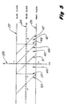
- the horizontal axis 24 measures time on the read clock.
- the vertical axis 29 measures the number of bits missed by the read clock.
- Horizontal lines 22 and 26 represent a read clock that is slow or fast, respectively, by the maximum correctable amount for the preferred embodiment.
- a disallowed pattern of the data channel code may be used.
- a more reliable solution is to add a header 32 (defined by slanting lines 31 and 33) of known content, such as a string of zeros, between the end of the data and the start 33 of the key 30.
- the maximum useful length of the header 32 is 2 b bits. Since the search for the key 30 begins b bits (27) prior to the anticipated start 29 of the key 30 this search will always be in the header 32, even when the start 33 of the key 30 appears b bits late due to a fast clock 26 during a data dropout.
- control circuitry 12 (as shown in Figure 1) will anticipate the start of the next data sub-block based on the read clock 24.
- a trailer 42 of length b bits must be appended to key 40 to delay the default (i. e., no key detected) start 48 of the next data sub-block. This provides adequate search time to detect the key 40 when bit slip has occurred due to a fast clock 26 and the key 40 appears late.
- the optimal fiducial mark size is thus k + 3b bits. This allows for a header 44 of 2b bits prior to the start 51 of the key 40 and a trailer 42 of b bits after the end 49 of the key 40.
- the key search begins b bits prior to the anticipated start 29 of the key 40.
- the key 40 bit pattern should be chosen to provide maximum orthogonality with the 2b non-key bit patterns that are part header 44 and part key 40.
Landscapes
- Engineering & Computer Science (AREA)
- General Engineering & Computer Science (AREA)
- Signal Processing (AREA)
- Signal Processing For Digital Recording And Reproducing (AREA)
Abstract
Description
- The present invention relates generally to digital signal recording systems and, more particularly, to a system having re-synchronizing signals separating blocks of recorded data to maintain precise read clock synchronization with a digital data stream.
- One of the significant problems in an information signal recording and reproducing system, such as a helical scan magnetic tape recorder, is the differences between the read and write clocks. It is desirable to have a fixed, continuously running clock for write operations. However, the write clock cannot be utilized to synchronize read operations because the read clock has to be synchronized to the data transitions read off the magnetic tape in order to properly decode the data. Several factors, such as data signal dropout, tape stretching, tape motion, the stability of the rotation of the drive motor and other differences between mechanisms, affect the frequency stability of the data transitions.
- Typically in signal recovery circuits a read clock is synchronized and phase-locked to the data transitions recorded on a recording media such as a magnetic disc or tape. This synchronization is effected with a burst of recorded synchronization signals, commonly referred to as a preamble, at the beginning of a data block. In some systems a synchronization signal referred to as a postamble is also included at the end of a data block. If a dropout in the signal occurs, for example, because of a flaw in the recording media, resulting in the temporary loss of the data signal, the read clock will no longer be phase-locked to the data transitions. When the signal returns, the read clock will require re-synchronization with the data signal. Slight speed variations in the system or drift of the clock frequency during the period of time that the read clock was not phase-locked may have caused the data stream to slip with respect to the read clock some integral number of bits or, in the case of a code such as Modified Frequency Modulation (MFM), some integral number of half bits.
- The resulting disagreement between expected bit numbers and actual bit numbers prevents successful decoding of the data. Consequently, the data is lost until the read clock is realigned with the data. A single bit slip will cause all subsequent bits to appear in error. Since a block of data is provided with a synchronization signal only at the beginning of the data block, a clock slip of one bit near the beginning of the data block will cause the loss of nearly all of the block of data.
- U. S. Patent No. 3,641,534 entitled "Intrarecord Resynchronization in Digital Recording Systems" issued to John W. Irwin on February 8, 1972, and assigned to International Business Machines Corporation, discloses a recording system which records a set of data signals, then records a set of resynchronization signals having predetermined signal phase and frequency-synchronizing and position-indicating components and repeats such recording steps until all data in one block has been recorded.
- The intrarecord re-synchronization system designed by Irwin reduces the amount of data lost by providing resynchronization marks between arbitrarily small sub-blocks of data within a block of recorded data; but does not provide for recovery of the data lost. Further, as the size of the sub-blocks decrease, the number of re-synchronization marks increase, and the throughput of the system is decreased.
- In accordance with the principles of the present invention, a magnetic tape recording and reproducing apparatus employing error correction and detection capability is provided. The data and error correction bits are recorded in sub-blocks which are separated by short re-synchronization signals. The number of bits in each sub-block is chosen such that the number of bits lost when a sub-block, or a multiple of sub-blocks, is lost is less than the total number of correctable bits provided by the error correction method utilized. In the preferred embodiment a data format utilizing a majority logic decodable highly interleaved error correction code and having re-synchronization or fiducial marks between successive sub-blocks of data provides a method of error correction which reduces the error-rate to an extremely low level. The recorded data bits and error-correction code bits are recorded in blocks comprised of sub-blocks that are lambda bits in length where lambda is the degree of interleave used. After every lambda bit sub-block a unique fiducial mark is inserted. Detection of this unique mark allows a bit counter to be updated thus re-synchronizing the data to a read clock. Thus, if the error correction code corrects t bits in each code word, the interleaved code can correct for the complete loss of any t consecutive sub-blocks. With independent re-synchronization of each sub-block any single loss of signal of length less than or equal to (t-1) × lambda bits can be corrected, even if clock synchronization is lost.
- A fiducial mark consists of a header, a key and a trailer in that order encoded in the same code (such as MFM) as the data. The key is a k bit pattern which identifies the start of the next data sub-block. At an appropriate time near the end of a data sub-block, control circuitry begins searching for the key. When the key is detected, it is then known that the next data sub-block begins a fixed number of bits later. This allows the control circuitry to correct for any slippage between the read clock and the data. A key must be sufficiently long and distinctive enough to be distinguished reliably from any non-key portions of the data stream that the key may be compared with. The key should also be short enough and simple enough to be easily identified when actually encountered by the control circuitry.
-
- Figure 1 is a simplified block diagram of a video tape recorder for recording and reproducing digital data according to the principles of the present invention.
- Figure 2 is a simplified diagrammatic representative of a data track recorded according to the principles of the present invention;
- Figure 3 is a diagrammatic representation of a fiducial mark according to the principles of the present invention;
- Figure 4 is a diagrammatic representation of a preferred embodiment of a fiducial mark; and
- Figure 5 is a diagrammatic representation of another preferred embodiment of a fiducial mark.
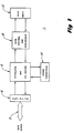
- Referring now to Figure 1, a magnetic tape recording and reproducing
device 1 including error correction and detection capability is provided.Interface bus 2 provides data words from a host system (not shown) in parallel format tointerface circuitry 4 which performs all interfacing functions including converting the input data into serial format. The errorcorrection logic circuit 6 provides the functions of data encoding and decoding for error correction purposes and interleaving of the code words. The coded words are 63 bits in length and comprise 45 bits of data and 18 check bits. - The error
correction logic circuit 6 comprises eighteen 912-bit shift registers (not shown) which form a linear feedback shift register which simultaneously performs code word generation and code word interleaving. A majority logic decodable error correction code which combines 45 data bits and 18 check bits into each code word is interleaved to degree 896 (lambda). The error correction code utilized is capable of correcting any three single bits in error in each code word. The errorcorrection logic circuit 6 formats each block of data and error correction code into sub-blocks of lambda bits and appends a string of 16 zeros to each such sub-block to reserve space for a fiducial mark to be added by thedata control circuitry 8. Thedata control circuitry 8 provides data write/head encoding and decoding functions and generates the data track preamble and the fiducial marks. - Referring now also to Figure 2, Miller Squared Frequency Modulation encoding is utilized to write the data on
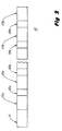
tracks 10 on the media (not shown) by the read/writecircuitry 12. Two blocks 13 and 17 of data are written on eachtrack 10 insub-blocks track 10, a highly redundant preamble 11 is generated by thedata control circuitry 8. Read synchronization is further ensured by inserting a unique 16-bitfiducial mark sub-block track 10,fiducial mark 19a which separates the two data blocks 13, 17 precedes thefirst data sub-block 17a in the second block 17. - During a read operation the detection of the
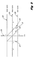
fiducial marks circuitry 12 updates a bit counter (not shown) which allows thedata control circuitry 8 to re-synchronize the read clock with the data stream if any bit slip has occurred. Decoded data is coupled to the errorcorrection logic circuitry 6 for de-interleaving and error detection. Any errors detected are corrected byerror correction circuitry 14. Since the error correction code is capable of correcting any three random bits in each 63 bit code word, the interleaved code allows the original data to be recovered as long as any burst error is confined to less than three sub-blocks (2688 bits). Even if clock synchronization is lost, any signal dropout oflength 2 lambda (1792) bits or less can be corrected. - The re-synchronization system is designed to correct for some maximum amount of bit slip, b, which will reduce the error rate to an acceptable level. The 16-bit fiducial mark utilized in the preferred embodiment allows re-synchronization after bit slips of up to + or - 4 bits. The fiducial mark is comprised of an eight-bit header, a four-bit key and a four-bit trailer, in that order. Referring now to Figure 3, the key 21 is a k bit pattern which identifies the start of the following data sub-block; for example,
fiducial mark 15a will identify the start of data sub-block 13b (as shown in Figure 2). At an appropriate time near the end of a data sub-block, control circuitry 12 (as shown in Figure 1) will begin looking for the key 21. When key 21 is detected, it is known that the data begins a fixed number of bits after the trailingedge 23, thus allowing thecontrol circuitry 12 to correct for any slippage between the read clock and the data. - Referring now to Figures 3, 4 and 5, the
horizontal axis 24 measures time on the read clock. Thevertical axis 29 measures the number of bits missed by the read clock.Horizontal lines lines 23 and 25) with the key length k, equal to four bits with the maximum correctable bit slip, b, equal to four bits. The fiducial mark will correct for + or - b bits missed. If theread clock 24 and the data agree, the trailingedge 23 of the key 21 is detected at t = 4. If the read clock runs slow (22) during a data dropout and misses b bits of data, the trailingedge 23 is detected early by b bits. Similarly, if the read clock runs fast (26) during a data dropout and assumes an extra b bits have passed, the trailingedge 23 will be detected late by b bits. - To detect the key 21 when the read clock has run slow (22) by the maximum correctable amount, the
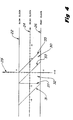
control circuitry 12 must begin searching for the key 21 b bits (as shown by dashed line 27) prior to the anticipated start (t = 0) of the key 21 (anticipated assuming that theread clock 24 and the data are synchronized). Beginning the search any earlier than b bits prior (27) to the anticipated start (29) of the key 21 increases the probability of incorrectly identifying a key in the data. "Beginning the search" at some time t means collecting the next k bits and comparing the collected bits with the key 21. This is most effectively done by passing the data through a k bit shift register. - Referring now specifically to Figure 4, to minimize inadvertent identification of a non-key portion of the data as a key, a disallowed pattern of the data channel code may be used. A more reliable solution is to add a header 32 (defined by slanting
lines 31 and 33) of known content, such as a string of zeros, between the end of the data and thestart 33 of the key 30. The maximum useful length of theheader 32 is 2 b bits. Since the search for the key 30 begins b bits (27) prior to theanticipated start 29 of the key 30 this search will always be in theheader 32, even when thestart 33 of the key 30 appears b bits late due to afast clock 26 during a data dropout. - Referring now specifically to Figure 5, if no key is detected, the control circuitry 12 (as shown in Figure 1) will anticipate the start of the next data sub-block based on the
read clock 24. Atrailer 42 of length b bits must be appended to key 40 to delay the default (i. e., no key detected) start 48 of the next data sub-block. This provides adequate search time to detect the key 40 when bit slip has occurred due to afast clock 26 and the key 40 appears late. - The optimal fiducial mark size is thus k + 3b bits. This allows for a
header 44 of 2b bits prior to the start 51 of the key 40 and atrailer 42 of b bits after theend 49 of the key 40. The key search begins b bits prior to theanticipated start 29 of the key 40. The key 40 bit pattern should be chosen to provide maximum orthogonality with the 2b non-key bit patterns that arepart header 44 andpart key 40. - Having described a specific preferred embodiment of the present invention with reference to the accompanying drawings, it is to be understood that the invention is not limited to the precise embodiment described, and that various changes and modifications may be affected therein by one skilled in the art without departing from the scope or spirit of the invention as defined in the appended claims.
Claims (8)
coding means (6) for coding and forming a block (13, 17) of a plurality of said data information words,
first means (6) for forming and adding a plurality of error check bits to each of said data information words,
second means (6) for forming each of said data information words and error check bits in said block (13,17) into a plurality of sub-blocks (13a,13b,...,17a,17b,....), each of said sub-blocks (13a,13b,...,17a,17b,....) having a predetermined number of bits, said predetermined number of bits being no greater than the number of bits correctable by said error correction code,
characterized by
third means (8) for forming a re-synchronization word (15a,15b,...,19a,19b,....) having a predetermined number of bits arranged in a recognizable unique bit pattern, said re-synchronization word (15a,15b,...,19a,19b,....) indicative of the position of the beginning of a sub-block (13a,13b,...,17a,17b,....),
recording means (12) for recording one of said plural ity of sub-blocks (13a,13b,...,17a,17b,....), then recording said re-synchronization word (15a,15b,...,19a,19b,....) and repeating such recording steps until all of said data information words and error check bits in said block (13,17) are recorded,
reading means (12) for reading said recorded block (13,17) of data information words and error check bits,
detecting means (12) for detecting said re-synchronization word (15a,15b,...,19a,19b,....),
means (8) responsive to said detected re-synchronization word (15a,15b,...,19a,19b,....) for synchronizing a read clock with said beginning of the succeeding sub-block (13a,13b,...,17a,17b,....), and
decoding means (6) for decoding said plurality of sub-blocks (13a,13b,...,17a,17b,....), said means (6) for decoding responsive to said plurality of error check bits for error detection and correction in said information words.
formatting a data stream in blocks (13,17) of a plurality of said data sub-blocks (13a,13b,...,17a,17b,....), having a predetermined number of bits,
characterized by the steps of
forming a re-synchronization signal (15a,15b,...,19a,19b,....) having a predetermined number of bits arranged in a recognizable unique bit pattern, indicative of the position of the beginning of said data sub-blocks (13a,13b,..., 17a, 17b, ....),
recording one of said plurality of data sub-blocks (13a,13b,...,17a,17b,....) and then recording said re-synchronization signal (15a,15b,...,19a,19b,....) and repeating such recording steps until all of said plurality of data sub-blocks (13a,13b,...,17a,17b,....) in each block (13,17) are recorded,
detecting said re-synchronization signal, and
synchronizing said read clock with the beginning of the next succeeding data sub-block (13a,13b,...,17a,17b,....) in response to said detected re-synchronization signal.
Applications Claiming Priority (2)
| Application Number | Priority Date | Filing Date | Title |
|---|---|---|---|
| US85104986A | 1986-04-11 | 1986-04-11 | |
| US851049 | 1986-04-11 |
Publications (1)
| Publication Number | Publication Date |
|---|---|
| EP0242093A1 true EP0242093A1 (en) | 1987-10-21 |
Family
ID=25309838
Family Applications (1)
| Application Number | Title | Priority Date | Filing Date |
|---|---|---|---|
| EP19870302930 Withdrawn EP0242093A1 (en) | 1986-04-11 | 1987-04-03 | Resynchronization of serial data blocks |
Country Status (2)
| Country | Link |
|---|---|
| EP (1) | EP0242093A1 (en) |
| JP (1) | JPS62241175A (en) |
Cited By (5)
| Publication number | Priority date | Publication date | Assignee | Title |
|---|---|---|---|---|
| EP0367217A1 (en) * | 1988-11-02 | 1990-05-09 | Hitachi, Ltd. | Information signal recording and playback method and apparatus therefor |
| EP0410722A2 (en) * | 1989-07-26 | 1991-01-30 | Sony Corporation | Information transmitting device |
| EP0420211A2 (en) * | 1989-09-29 | 1991-04-03 | Kabushiki Kaisha Toshiba | Optical disk apparatus |
| EP0438355A1 (en) * | 1990-01-17 | 1991-07-24 | Fujitsu Limited | Method for reading a synchronizing signal from a record medium and an apparatus therefor |
| EP0473293A1 (en) * | 1990-08-03 | 1992-03-04 | Canon Kabushiki Kaisha | Synchronous signal detection circuit and synchronous signal detection apparatus having the same |
Citations (4)
| Publication number | Priority date | Publication date | Assignee | Title |
|---|---|---|---|---|
| US3641534A (en) * | 1969-12-29 | 1972-02-08 | Ibm | Intrarecord resynchronization in digital-recording systems |
| EP0133790A1 (en) * | 1983-07-30 | 1985-03-06 | Sony Corporation | Disc playback apparatus |
| EP0164746A2 (en) * | 1984-06-15 | 1985-12-18 | Matsushita Electric Industrial Co., Ltd. | Optical information recording and reproducing apparatus and optical disc |
| EP0166785A1 (en) * | 1983-12-16 | 1986-01-08 | Sony Corporation | Disk reproducing apparatus |
-
1987
- 1987-04-03 EP EP19870302930 patent/EP0242093A1/en not_active Withdrawn
- 1987-04-08 JP JP8670087A patent/JPS62241175A/en active Pending
Patent Citations (4)
| Publication number | Priority date | Publication date | Assignee | Title |
|---|---|---|---|---|
| US3641534A (en) * | 1969-12-29 | 1972-02-08 | Ibm | Intrarecord resynchronization in digital-recording systems |
| EP0133790A1 (en) * | 1983-07-30 | 1985-03-06 | Sony Corporation | Disc playback apparatus |
| EP0166785A1 (en) * | 1983-12-16 | 1986-01-08 | Sony Corporation | Disk reproducing apparatus |
| EP0164746A2 (en) * | 1984-06-15 | 1985-12-18 | Matsushita Electric Industrial Co., Ltd. | Optical information recording and reproducing apparatus and optical disc |
Cited By (16)
| Publication number | Priority date | Publication date | Assignee | Title |
|---|---|---|---|---|
| EP0710956A1 (en) * | 1988-11-02 | 1996-05-08 | Hitachi, Ltd. | Information signal reproducing apparatus and information signal reproducing method |
| US7019927B2 (en) | 1988-11-02 | 2006-03-28 | Hitachi, Ltd. | Information signal recording and playback method and apparatus therefor |
| US6657831B2 (en) | 1988-11-02 | 2003-12-02 | Hitachi, Ltd. | Information signal recording and playback method and apparatus therefor |
| EP0367217A1 (en) * | 1988-11-02 | 1990-05-09 | Hitachi, Ltd. | Information signal recording and playback method and apparatus therefor |
| US6424477B1 (en) | 1988-11-02 | 2002-07-23 | Hitachi, Ltd. | Information signal recording and playback method and apparatus therefor |
| US5956193A (en) * | 1988-11-02 | 1999-09-21 | Hitachi, Ltd. | Information signal recording and playback method and apparatus therefor |
| US5589995A (en) * | 1988-11-02 | 1996-12-31 | Hitachi, Ltd. | Header information of information signal recording and reproducing method and apparatus therefor |
| EP0410722A2 (en) * | 1989-07-26 | 1991-01-30 | Sony Corporation | Information transmitting device |
| EP0410722A3 (en) * | 1989-07-26 | 1994-01-26 | Sony Corp | |
| EP0420211A3 (en) * | 1989-09-29 | 1992-02-19 | Kabushiki Kaisha Toshiba | Optical disk apparatus |
| US5218590A (en) * | 1989-09-29 | 1993-06-08 | Kabushiki Kaisha Toshiba | Optical disk apparatus having improved recording capacity |
| EP0420211A2 (en) * | 1989-09-29 | 1991-04-03 | Kabushiki Kaisha Toshiba | Optical disk apparatus |
| US5604723A (en) * | 1990-01-17 | 1997-02-18 | Fujitsu Limited | Method for reading a synchronizing signal from a record medium and an apparatus thereof |
| EP0438355A1 (en) * | 1990-01-17 | 1991-07-24 | Fujitsu Limited | Method for reading a synchronizing signal from a record medium and an apparatus therefor |
| US5446715A (en) * | 1990-08-03 | 1995-08-29 | Canon Kabushiki Kaisha | Circuit for detecting a synchronous signal included in an information signal |
| EP0473293A1 (en) * | 1990-08-03 | 1992-03-04 | Canon Kabushiki Kaisha | Synchronous signal detection circuit and synchronous signal detection apparatus having the same |
Also Published As
| Publication number | Publication date |
|---|---|
| JPS62241175A (en) | 1987-10-21 |
Similar Documents
| Publication | Publication Date | Title |
|---|---|---|
| JP3280335B2 (en) | Data recording medium and data recording encoder | |
| JP3083011B2 (en) | Data recording method and device | |
| EP1083687B1 (en) | Method and device for modulating and demodulating data using a variable length code | |
| JPH07254231A (en) | Recording medium, signal recorder and reproducer for the medium | |
| KR100393386B1 (en) | Run length limited encoding/decoding with robust resync | |
| JPH0656694B2 (en) | Signal transfer device | |
| JP3428039B2 (en) | Synchronous signal detector, synchronous signal detecting method and decoding device | |
| KR100633498B1 (en) | Method, system, and recording medium containing program for synchronization and resynchronization of a data stream | |
| US4183066A (en) | Technique for recording data on magnetic disks at plural densities | |
| US5379160A (en) | Magnetic disk drive apparatus including improved decoding circuit | |
| EP0242093A1 (en) | Resynchronization of serial data blocks | |
| US3821798A (en) | Resynchronizable recording system | |
| EP0318227A2 (en) | Frame synchronising method and system | |
| US5264970A (en) | Digital signal reproducing apparatus | |
| US6574756B1 (en) | Method and apparatus for identifying the start of a data field using a fault tolerant sync word | |
| US6583941B1 (en) | Method and apparatus for thermal asperity recovery for word sync detection in data channels | |
| KR20030026367A (en) | Data transfer method, block synchronizing signal detecting method, and reproducing apparatus | |
| US7167524B2 (en) | Method of inserting sync data in modulated data and recording medium containing the sync data | |
| US7248557B2 (en) | Robust header configuration and method for reading sector identifiers contained therein | |
| CN1042783C (en) | Transmission method for binary signal | |
| JP3903569B2 (en) | Recording / playback method | |
| CA2112452C (en) | Enhanced data formats and machine operations for enabling error correction | |
| US6707627B1 (en) | Error checking in a disk drive system using a modulo code | |
| JPH0991885A (en) | Synchronous information adding method and synchronous information adding device, and synchronous information detecting method and synchronous information detecting device | |
| JP2658741B2 (en) | Optical recording / reproducing method |
Legal Events
| Date | Code | Title | Description |
|---|---|---|---|
| PUAI | Public reference made under article 153(3) epc to a published international application that has entered the european phase |
Free format text: ORIGINAL CODE: 0009012 |
|
| AK | Designated contracting states |
Kind code of ref document: A1 Designated state(s): DE FR GB IT |
|
| 17P | Request for examination filed |
Effective date: 19880323 |
|
| 17Q | First examination report despatched |
Effective date: 19900130 |
|
| STAA | Information on the status of an ep patent application or granted ep patent |
Free format text: STATUS: THE APPLICATION IS DEEMED TO BE WITHDRAWN |
|
| 18D | Application deemed to be withdrawn |
Effective date: 19900612 |
|
| RIN1 | Information on inventor provided before grant (corrected) |
Inventor name: WINTERS KEL D. Inventor name: BROMLEY DAVID J. Inventor name: BAUGH RICHARD A. Inventor name: SPENNER BRUCE F. |