EP0213843A2 - Digital processor control - Google Patents
Digital processor control Download PDFInfo
- Publication number
- EP0213843A2 EP0213843A2 EP86306268A EP86306268A EP0213843A2 EP 0213843 A2 EP0213843 A2 EP 0213843A2 EP 86306268 A EP86306268 A EP 86306268A EP 86306268 A EP86306268 A EP 86306268A EP 0213843 A2 EP0213843 A2 EP 0213843A2
- Authority
- EP
- European Patent Office
- Prior art keywords
- register
- operand
- location
- registers
- predetermined
- Prior art date
- Legal status (The legal status is an assumption and is not a legal conclusion. Google has not performed a legal analysis and makes no representation as to the accuracy of the status listed.)
- Granted
Links
- 238000000034 method Methods 0.000 claims abstract description 59
- 238000004891 communication Methods 0.000 claims description 8
- 230000007274 generation of a signal involved in cell-cell signaling Effects 0.000 claims 2
- 230000007246 mechanism Effects 0.000 description 6
- 230000004913 activation Effects 0.000 description 4
- 230000008901 benefit Effects 0.000 description 3
- 238000010586 diagram Methods 0.000 description 2
- 230000000246 remedial effect Effects 0.000 description 2
- 230000009471 action Effects 0.000 description 1
- 238000001514 detection method Methods 0.000 description 1
- 229920005669 high impact polystyrene Polymers 0.000 description 1
- 239000004797 high-impact polystyrene Substances 0.000 description 1
- 230000004048 modification Effects 0.000 description 1
- 238000012986 modification Methods 0.000 description 1
- 239000002699 waste material Substances 0.000 description 1
Images

Classifications
-
- G—PHYSICS
- G06—COMPUTING; CALCULATING OR COUNTING
- G06F—ELECTRIC DIGITAL DATA PROCESSING
- G06F9/00—Arrangements for program control, e.g. control units
- G06F9/06—Arrangements for program control, e.g. control units using stored programs, i.e. using an internal store of processing equipment to receive or retain programs
- G06F9/46—Multiprogramming arrangements
- G06F9/468—Specific access rights for resources, e.g. using capability register
-
- G—PHYSICS
- G06—COMPUTING; CALCULATING OR COUNTING
- G06F—ELECTRIC DIGITAL DATA PROCESSING
- G06F12/00—Accessing, addressing or allocating within memory systems or architectures
- G06F12/14—Protection against unauthorised use of memory or access to memory
- G06F12/1458—Protection against unauthorised use of memory or access to memory by checking the subject access rights
-
- G—PHYSICS
- G06—COMPUTING; CALCULATING OR COUNTING
- G06F—ELECTRIC DIGITAL DATA PROCESSING
- G06F9/00—Arrangements for program control, e.g. control units
- G06F9/06—Arrangements for program control, e.g. control units using stored programs, i.e. using an internal store of processing equipment to receive or retain programs
- G06F9/44—Arrangements for executing specific programs
- G06F9/448—Execution paradigms, e.g. implementations of programming paradigms
- G06F9/4482—Procedural
- G06F9/4484—Executing subprograms
-
- G—PHYSICS
- G06—COMPUTING; CALCULATING OR COUNTING
- G06F—ELECTRIC DIGITAL DATA PROCESSING
- G06F9/00—Arrangements for program control, e.g. control units
- G06F9/06—Arrangements for program control, e.g. control units using stored programs, i.e. using an internal store of processing equipment to receive or retain programs
- G06F9/46—Multiprogramming arrangements
- G06F9/461—Saving or restoring of program or task context
- G06F9/462—Saving or restoring of program or task context with multiple register sets
Definitions
- This invention relates to storage elements of digital computers, and more particularly, to a high-speed general-purpose register file for use with a reduced instruction-set computer providing ready parameter-passing between procedures and a protection mechanism supporting multiple tasks.
- Reduced instruction set computers recognize the advantages of employing a set of high-speed, general-purpose registers for the storage of often-used data in conjunction with a lower-speed main memory for the storge of less-frequently used data.
- Run-time studies of programs indicate that the data most often-used in procedures are typically simple, non-array variables, and not in excess of thirty-two such variables are used with a procedure.
- the Berkeley RISC machines RISC I and RISC II, the Stanford HIPS machine, and the IBM 801 are representative of RISC architectures.
- a stack is used in allocating and deallocating activation records whenever a procedure of a high-level language (HLL) is invoked or returned from, respectively.
- the activation record includes portions for incoming parameters (variables), purely local variables, and outgoing parameters (variables).
- the portion allocated to the outgoing parameters of one activation record of a procedure may be overlapped with the portion allocated to the incoming parameters of another activation record of another procedure so that parameter values may be efficiently communicated between the procedures.
- a compiler for a HLL arranges data references within a procedure so that most references are to the high-speed registers to improve performance.
- RISC architecture machines contain a set of high-speed registers which exceeds the number required for the storage of often-needed data within any given procedure, for example, thirty-two registers.
- the Berkeley RISC machines assign a fixed number of registers to a procedure ("window"). Since this number is generally larger than that actually required by a procedure, waste of registers is inevitable.
- the instruction processor to be described provides a high-speed register file in which only that number of registers required by a procedure is allocated to it. Registers which are in excess of those required for a given procedure may be used to store variables for other procedures or tasks. Communication between multiple procedures may occur via variables contained in a set of so-called “global” registers, while variables required for a given procedure are stored in a set of so-called “local” registers, each set with its own address space.
- Parameters may be passed from a calling procedure to a called procedure via a stack mechanism. Accesses to local registers are relative to a stack pointer value stored in a register. The contents of the stack pointer register may be adjusted so that the set of registers used by a calling and a called procedure overlap and communication therebetween is via the registers in common.
- a register protection mechanism supports a multi-tasking environment fn which each task maintains integrity from any undesired changes occuring in other tasks.
- the protection mechanism proscribes access of certain registers within the high-speed register file during the execution of a particular procedure or task.
- the register file is divided into a number of "blocks" of contiguous registers.
- a protection register contains a binary word each bit position of which can be set to either permit access or deny access to the block corresponding to the particular bit position.
- An attempt by an instruction to access a register within a protected block causes a machine "fault" and appropriate remedial action is undertaken. Accordingly, variables for multiple tasks can be stored in separate blocks within the register file, the variables for each task protected from access by other tasks.
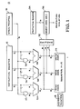
- Fig. 1 a block diagram of the control portion of an instruction processor 10 utilized in a reduced instruction set computer (RISC). While the register file will be explained herein in connection with processor 10, this is for the purposes of illustration only, and the various benefits and advantages provided by the register file are available in a wide range of applications, as will be appreciated by those skilled in the art.
- RISC reduced instruction set computer
- processor 10 includes an instruction register 12 which stores the processor instruction, in binary form, which has been fetched from an instruction cache, not shown.
- Most processor instructions specify a pair of operands, being the two sources of data to be processed, and a third operand, being the destination where the resulting value is to be stored.
- these operands are in registers located within the register file 14, of the present invention.
- the file in the preferred embodiment, contains 128 so-called “global" registers for storage of simple, non-array, variables common to several procedures and 128 so-called "local" registers for storage of simple variables and parameters used within a single procedure.
- the register file 14 is intended for storage of often-used data, as will be explained below.
- register file 14 Although shown external to register file 14, the processor 10 contains a stack pointer (SP) register 16 which is located within file 14 as register number 3, and an indirect pointer (IP) register 18 as register number 2.
- register file 14 also contains as register number 1, a register which when specified in an instruction causes the local register within file 14 whose address is stored in bit positions 2-8 of the IP register 18 to be accessed.
- register number 1 a register which when specified causes the global register within file 14 whose address is stored in bit positions 2-8 of the IP register to be accessed.
- Signals representing the operand portions of the instruction stored in instruction register 12 are conducted to one of three two-input summers: a first summer 20 receives at a first input signal representing the first operand of the instruction stored in register 12 and signals representing the contents of the SP register 16 are conducted to a second input of summer 20 via an AND gate 22.
- AND gate 22 also receives a signal corresponding to the most significant bit (msb) of the first operand of the instruction stored in register 12.
- a second summer 24 and a third summer 28 receive at a first input signals representing the second and third operand, respectively, of the instruction stored in register 12 and signals representing the contents of the SP register 16 are conducted to a second input of summers 24 and 28 via AND gates 26 and 30, respectively.
- AND gate 26 and AND gate 30 also receive a signal corresponding to the msb of the second, and third, respectively, operand of the instruction stored in register 12.
- Signals generated at an output of summers 20 and 24 are conducted to a first and second, respectively, read address (READ_ADDR) input of register file 14, as well as to a first and second, respectively, input to a decode circuit 32.
- Signals generated at an output of summer 28 are conducted to a write address (WRITE_ADDR) input of register file 14, as well as to a third input of decode circuit 32.
- a protection register 34 contains information which specifies which of certain registers within register file 14 may be accessed by the instruction stored in register 12, as will be described below in connection with Fig. 3. Signals representing this protection information are conducted to a combinatorial select circuit 36 which also receives signals generated by the decode circuit 32. Select circuit 36 generates at an output a signal indicative of an attempt by the instruction in register 12 to access a particular register in file 14 which is protected according to the contents of protection register 34. A computer "fault" would be detected in this event and appropriate action would be undertaken.
- SP register 16 and the IP register 18 are best described in conjunction with Table I, below.
- Table I Four modes of addressing the registers within file 14 are permitted by processor control 10, and they are determined by the value n shown in the first column of Table I as specified by the operands of the instruction stored in register 12.
- references to "local" registers within file 14 are relative to the contents of the SP register 16, in accordance with row four of Table I. Hence access to local registers may be adjusted so that the set of contiguous registers with file 14 used by one procedure may overlap those used by another procedure as will be described below in connection with Fig. 2.
- the set of local registers within file 14 used by a pair of nested procedures A and B, will be described with reference to Fig. 2.
- procedure A the contents of the SP register 16 is set to point to a particular local register 100.
- registers 100, 102, 104 and 106 are allocated for variables purely local to procedure A.
- procedure B the contents of the SP register 16 is set to point to local register 108.
- local registers 108, 110 and 112 were allocated to procedure A for variables common to both procedure A and procedure B.
- communication between these procedures is by way of local registers 108, 110 and 112.
- Local registers 114, 116, ..., 130 are allocated for variables purely local to procedure B, although if a procedure C were to be called from procedure B, a set of the latter registers ending with 130 may be used for communication between procedures B and C by setting the contents of SP register 16 so as to point to a local register 114, ..., 130.
- communication between multiple procedures may occur via variables stored in the "global" register portion of file 14, i.e., those registers in file 14 having addresses 2 through 127.
- the register file 14 of the instant invention is preferably -4 used in conjunction with a protection mechanism afforded by the protection register 34 illustrated in Fig. 3.
- register file 14 consists of 256 registers divided into 16 blocks of 16 contiguous registers each.
- the protection register 34 comprises a 16-bit register capable of storing a 16-bit binary value specifying by, for example, a binary ONE, that a particular block is proscribed access.
- An exemplary coding technique is shown in Fig. 3 in which the msb, position 15, of register 34 corresponds to the block of registers having addresses with file 14 of 0 through 15, inclusive, position 14 corresponds to the block of registers having addresses 16 through 31, etc.
- the effective address of the operands are conducted to decode circuit 32 and a comparison made by select circuit 36 between the operand addresses and the proscribed addresses as specified by the contents of register 34.
- the select circuit 36 generates a protection violation signal upon detection of an attempt to access a proscribed register within file 14 and a "fault" is generated which interrupts processing of the instruction by processor 10 so that remedial action may be undertaken.
- variables for multiple tasks may be simultaneously stored within register file 14 within different blocks, and variables for each task will be protected from access by other tasks.
Abstract
Description
- This invention relates to storage elements of digital computers, and more particularly, to a high-speed general-purpose register file for use with a reduced instruction-set computer providing ready parameter-passing between procedures and a protection mechanism supporting multiple tasks.
- Reduced instruction set computers (RISC) recognize the advantages of employing a set of high-speed, general-purpose registers for the storage of often-used data in conjunction with a lower-speed main memory for the storge of less-frequently used data. Run-time studies of programs indicate that the data most often-used in procedures are typically simple, non-array variables, and not in excess of thirty-two such variables are used with a procedure. The Berkeley RISC machines RISC I and RISC II, the Stanford HIPS machine, and the IBM 801 are representative of RISC architectures.
- At run-time, a stack is used in allocating and deallocating activation records whenever a procedure of a high-level language (HLL) is invoked or returned from, respectively. The activation record includes portions for incoming parameters (variables), purely local variables, and outgoing parameters (variables). The portion allocated to the outgoing parameters of one activation record of a procedure may be overlapped with the portion allocated to the incoming parameters of another activation record of another procedure so that parameter values may be efficiently communicated between the procedures.
- A compiler for a HLL arranges data references within a procedure so that most references are to the high-speed registers to improve performance. RISC architecture machines contain a set of high-speed registers which exceeds the number required for the storage of often-needed data within any given procedure, for example, thirty-two registers. The Berkeley RISC machines assign a fixed number of registers to a procedure ("window"). Since this number is generally larger than that actually required by a procedure, waste of registers is inevitable.
- Ideally, only the number of registers actually required by a procedure should be allocated for it and the registers in excess of those required could be used to store variables for communication between procedures, and for other tasks.
- The instruction processor to be described provides a high-speed register file in which only that number of registers required by a procedure is allocated to it. Registers which are in excess of those required for a given procedure may be used to store variables for other procedures or tasks. Communication between multiple procedures may occur via variables contained in a set of so-called "global" registers, while variables required for a given procedure are stored in a set of so-called "local" registers, each set with its own address space.
- Parameters may be passed from a calling procedure to a called procedure via a stack mechanism. Accesses to local registers are relative to a stack pointer value stored in a register. The contents of the stack pointer register may be adjusted so that the set of registers used by a calling and a called procedure overlap and communication therebetween is via the registers in common.
- A register protection mechanism supports a multi-tasking environment fn which each task maintains integrity from any undesired changes occuring in other tasks. The protection mechanism proscribes access of certain registers within the high-speed register file during the execution of a particular procedure or task. The register file is divided into a number of "blocks" of contiguous registers. A protection register contains a binary word each bit position of which can be set to either permit access or deny access to the block corresponding to the particular bit position. An attempt by an instruction to access a register within a protected block causes a machine "fault" and appropriate remedial action is undertaken. Accordingly, variables for multiple tasks can be stored in separate blocks within the register file, the variables for each task protected from access by other tasks.
-
- Fig. 1 is a block diagram of an instruction processor employing a register file of the instant invention;
- Fig. 2 illustrates the use of a stack pointer in allocating local registers in the file of the instant invention; and
- Fig. 3 illustrates the protection register used in conjunction with the register file of the instant invention.
- The register file of the instant invention is best understood with reference to Fig. 1, a block diagram of the control portion of an
instruction processor 10 utilized in a reduced instruction set computer (RISC). While the register file will be explained herein in connection withprocessor 10, this is for the purposes of illustration only, and the various benefits and advantages provided by the register file are available in a wide range of applications, as will be appreciated by those skilled in the art. - As shown in Fig. 1,
processor 10 includes aninstruction register 12 which stores the processor instruction, in binary form, which has been fetched from an instruction cache, not shown. Most processor instructions specify a pair of operands, being the two sources of data to be processed, and a third operand, being the destination where the resulting value is to be stored. Normally, these operands are in registers located within theregister file 14, of the present invention. The file, in the preferred embodiment, contains 128 so-called "global" registers for storage of simple, non-array, variables common to several procedures and 128 so-called "local" registers for storage of simple variables and parameters used within a single procedure. Theregister file 14 is intended for storage of often-used data, as will be explained below. - Although shown external to register
file 14, theprocessor 10 contains a stack pointer (SP)register 16 which is located withinfile 14 as register number 3, and an indirect pointer (IP)register 18 as register number 2. Registerfile 14 also contains as register number 1, a register which when specified in an instruction causes the local register withinfile 14 whose address is stored in bit positions 2-8 of theIP register 18 to be accessed. As register number 0, a register withinfile 14 which when specified causes the global register withinfile 14 whose address is stored in bit positions 2-8 of the IP register to be accessed. Signals representing the operand portions of the instruction stored ininstruction register 12 are conducted to one of three two-input summers: afirst summer 20 receives at a first input signal representing the first operand of the instruction stored inregister 12 and signals representing the contents of theSP register 16 are conducted to a second input ofsummer 20 via anAND gate 22. ANDgate 22 also receives a signal corresponding to the most significant bit (msb) of the first operand of the instruction stored inregister 12. - A second summer 24 and a
third summer 28 receive at a first input signals representing the second and third operand, respectively, of the instruction stored inregister 12 and signals representing the contents of theSP register 16 are conducted to a second input ofsummers 24 and 28 via ANDgates gate 26 and ANDgate 30 also receive a signal corresponding to the msb of the second, and third, respectively, operand of the instruction stored inregister 12. - Signals generated at an output of
summers 20 and 24 are conducted to a first and second, respectively, read address (READ_ADDR) input ofregister file 14, as well as to a first and second, respectively, input to adecode circuit 32. Signals generated at an output ofsummer 28 are conducted to a write address (WRITE_ADDR) input ofregister file 14, as well as to a third input ofdecode circuit 32. - A
protection register 34 contains information which specifies which of certain registers withinregister file 14 may be accessed by the instruction stored inregister 12, as will be described below in connection with Fig. 3. Signals representing this protection information are conducted to a combinatorialselect circuit 36 which also receives signals generated by thedecode circuit 32. Selectcircuit 36 generates at an output a signal indicative of an attempt by the instruction inregister 12 to access a particular register infile 14 which is protected according to the contents ofprotection register 34. A computer "fault" would be detected in this event and appropriate action would be undertaken. In this manner, quick switching from one task to another in a multi-tasking environment is facilitated so that variables for each task are protected from access by other tasks by the ability to proscribe access of certain registers withinfile 14 by specifying a particular bit pattern inprotection register 34, as will be described below in connection with Fig. 3. - The operation of the
SP register 16 and theIP register 18 is best described in conjunction with Table I, below. Four modes of addressing the registers withinfile 14 are permitted byprocessor control 10, and they are determined by the value n shown in the first column of Table I as specified by the operands of the instruction stored inregister 12.
- An instruction having an operand, n, 2<=n<=127, will refer to the "global" register within
file 14 located at the address n withinfile 14. Since the msb in the eight-bit binary representation of n will be ZERO in this case, thesummer AND gate register 12 will be generated without modification at the output ofsummer file 14 will be used for reading or writing, as the signals generated bysummer file 14 or the WRITE_ADDR input offile 14, in accordance with row three of Table I. - An instruction having an operand, n, 128<=n<=255, will have an eight-bit binary representation in which the msb will be ONE and the
AND gate SP register 16 to the second input ofsummer register 12 will be increased by the value in theSP register 16 insummer file 14 are relative to the contents of theSP register 16, in accordance with row four of Table I. Hence access to local registers may be adjusted so that the set of contiguous registers withfile 14 used by one procedure may overlap those used by another procedure as will be described below in connection with Fig. 2. - By specifying with the instruction stored in register 12 a register value n of 0, reference is had to the global register within
file 14 whose address is stored in bit positions 2-8 of the IP registerr18, in accordance with row one of Table I. And specifying a value of 1 for n, reference is had to the local register withinfile 14 whose address is stored in bit positions 2-8 of theIP register 18, in accordance with row two of Table I. The mechanism by which this "indirect" addressing mode is implemented is well known,to those skilled in the art and will not be described herein. - The set of local registers within
file 14 used by a pair of nested procedures A and B, will be described with reference to Fig. 2. Upon entry to procedure A the contents of theSP register 16 is set to point to a particularlocal register 100. For the procedure A illustrated in Fig. 2,registers SP register 16 is set to point tolocal register 108. However,local registers local registers Local registers local register 114, ..., 130. - In addition to the inter-procedural communication illustrated in Fig. 2, communication between multiple procedures may occur via variables stored in the "global" register portion of
file 14, i.e., those registers infile 14 having addresses 2 through 127. - The
register file 14 of the instant invention is preferably -4 used in conjunction with a protection mechanism afforded by theprotection register 34 illustrated in Fig. 3. In the preferred embodiment, registerfile 14 consists of 256 registers divided into 16 blocks of 16 contiguous registers each. Theprotection register 34 comprises a 16-bit register capable of storing a 16-bit binary value specifying by, for example, a binary ONE, that a particular block is proscribed access. An exemplary coding technique is shown in Fig. 3 in which the msb,position 15, ofregister 34 corresponds to the block of registers having addresses withfile 14 of 0 through 15, inclusive,position 14 corresponds to the block ofregisters having addresses 16 through 31, etc. - During the decoding of the instruction stored in
register 12, the effective address of the operands are conducted to decodecircuit 32 and a comparison made byselect circuit 36 between the operand addresses and the proscribed addresses as specified by the contents ofregister 34. Theselect circuit 36 generates a protection violation signal upon detection of an attempt to access a proscribed register withinfile 14 and a "fault" is generated which interrupts processing of the instruction byprocessor 10 so that remedial action may be undertaken. - In this manner variables for multiple tasks may be simultaneously stored within
register file 14 within different blocks, and variables for each task will be protected from access by other tasks.
Claims (12)
Priority Applications (1)
| Application Number | Priority Date | Filing Date | Title |
|---|---|---|---|
| AT86306268T ATE85713T1 (en) | 1985-08-30 | 1986-08-14 | DIGITAL PROCESSOR CONTROL. |
Applications Claiming Priority (2)
| Application Number | Priority Date | Filing Date | Title |
|---|---|---|---|
| US771311 | 1985-08-30 | ||
| US06/771,311 US4777588A (en) | 1985-08-30 | 1985-08-30 | General-purpose register file optimized for intraprocedural register allocation, procedure calls, and multitasking performance |
Publications (3)
| Publication Number | Publication Date |
|---|---|
| EP0213843A2 true EP0213843A2 (en) | 1987-03-11 |
| EP0213843A3 EP0213843A3 (en) | 1989-03-29 |
| EP0213843B1 EP0213843B1 (en) | 1993-02-10 |
Family
ID=25091411
Family Applications (1)
| Application Number | Title | Priority Date | Filing Date |
|---|---|---|---|
| EP86306268A Expired - Lifetime EP0213843B1 (en) | 1985-08-30 | 1986-08-14 | Digital processor control |
Country Status (5)
| Country | Link |
|---|---|
| US (1) | US4777588A (en) |
| EP (1) | EP0213843B1 (en) |
| JP (1) | JP2678183B2 (en) |
| AT (1) | ATE85713T1 (en) |
| DE (1) | DE3687724T2 (en) |
Cited By (4)
| Publication number | Priority date | Publication date | Assignee | Title |
|---|---|---|---|---|
| WO1993001543A1 (en) * | 1991-07-08 | 1993-01-21 | S-Mos Systems, Inc. | Risc microprocessor architecture implementing multiple typed register sets |
| WO2000033188A2 (en) * | 1998-12-03 | 2000-06-08 | Sun Microsystems, Inc. | Efficient handling of a large register file for context switching and function calls and returns |
| US7114056B2 (en) | 1998-12-03 | 2006-09-26 | Sun Microsystems, Inc. | Local and global register partitioning in a VLIW processor |
| US7117342B2 (en) | 1998-12-03 | 2006-10-03 | Sun Microsystems, Inc. | Implicitly derived register specifiers in a processor |
Families Citing this family (35)
| Publication number | Priority date | Publication date | Assignee | Title |
|---|---|---|---|---|
| JP2545789B2 (en) * | 1986-04-14 | 1996-10-23 | 株式会社日立製作所 | Information processing device |
| US5293594A (en) * | 1986-05-24 | 1994-03-08 | Hitachi, Ltd. | Data processing system having a plurality of register groups and a logical or circuit for addressing one register of one of the register groups |
| US4853849A (en) * | 1986-12-17 | 1989-08-01 | Intel Corporation | Multi-tasking register set mapping system which changes a register set pointer block bit during access instruction |
| DE3726192A1 (en) * | 1987-08-06 | 1989-02-16 | Otto Mueller | STACK CONTROL |
| US5513353A (en) * | 1987-09-30 | 1996-04-30 | Kabushiki Kaisha Toshiba | Cache control system which permanently inhibits local but not global parameter data writes to main memory |
| JPH01263728A (en) * | 1988-04-14 | 1989-10-20 | Sharp Corp | Microprocessor equipped with relative instructable register group |
| JP3034873B2 (en) * | 1988-07-01 | 2000-04-17 | 株式会社日立製作所 | Information processing device |
| US5321823A (en) * | 1988-07-20 | 1994-06-14 | Digital Equipment Corporation | Digital processor with bit mask for counting registers for fast register saves |
| US5083263A (en) * | 1988-07-28 | 1992-01-21 | Sun Microsystems, Inc. | BISC with interconnected register ring and selectively operating portion of the ring as a conventional computer |
| US5159680A (en) * | 1988-07-28 | 1992-10-27 | Sun Microsystems, Inc. | Risc processing unit which selectively isolates register windows by indicating usage of adjacent register windows in status register |
| JPH0630063B2 (en) * | 1989-02-17 | 1994-04-20 | 株式会社東芝 | Microprocessor |
| JP2655191B2 (en) * | 1989-07-05 | 1997-09-17 | 三菱電機株式会社 | Arithmetic processing unit |
| JPH0353328A (en) * | 1989-07-20 | 1991-03-07 | Hitachi Ltd | Register saving recoverying method and processor |
| JP2991242B2 (en) * | 1989-10-12 | 1999-12-20 | テキサス インスツルメンツ インコーポレーテッド | How to use a multiprocessor computer system |
| US5428793A (en) * | 1989-11-13 | 1995-06-27 | Hewlett-Packard Company | Method and apparatus for compiling computer programs with interproceduural register allocation |
| US5522072A (en) * | 1990-09-04 | 1996-05-28 | At&T Corp. | Arrangement for efficiently transferring program execution between subprograms |
| US5226142A (en) * | 1990-11-21 | 1993-07-06 | Ross Technology, Inc. | High performance register file with overlapping windows |
| US5696957A (en) * | 1991-05-17 | 1997-12-09 | Ricoh Company, Ltd | Integrated circuit comprising a central processing unit for executing a plurality of programs |
| US5539911A (en) | 1991-07-08 | 1996-07-23 | Seiko Epson Corporation | High-performance, superscalar-based computer system with out-of-order instruction execution |
| EP0636256B1 (en) | 1992-03-31 | 1997-06-04 | Seiko Epson Corporation | Superscalar risc processor instruction scheduling |
| DE69308548T2 (en) | 1992-05-01 | 1997-06-12 | Seiko Epson Corp | DEVICE AND METHOD FOR COMPLETING THE COMMAND IN A SUPER-SCALAR PROCESSOR. |
| US5628021A (en) | 1992-12-31 | 1997-05-06 | Seiko Epson Corporation | System and method for assigning tags to control instruction processing in a superscalar processor |
| GB2278698B (en) * | 1993-05-05 | 1997-09-03 | Hewlett Packard Co | Multi-ported data storage device with improved cell stability |
| JP3676411B2 (en) * | 1994-01-21 | 2005-07-27 | サン・マイクロシステムズ・インコーポレイテッド | Register file device and register file access method |
| EP0676691A3 (en) * | 1994-04-06 | 1996-12-11 | Hewlett Packard Co | Apparatus for register saving and restoring in a digital computer. |
| US5655132A (en) * | 1994-08-08 | 1997-08-05 | Rockwell International Corporation | Register file with multi-tasking support |
| US6086632A (en) * | 1996-10-31 | 2000-07-11 | Nec Corporation | Register optimizing compiler using commutative operations |
| JP2000353092A (en) * | 1999-06-09 | 2000-12-19 | Nec Corp | Information processor and register file switching method for the processor |
| JP2002182927A (en) * | 2000-12-13 | 2002-06-28 | Hitachi Ltd | Allocating method of register in different execution environment, software developing method in different execution environment and lsi in which program to execute the same is incorporated |
| US20020099872A1 (en) * | 2001-01-19 | 2002-07-25 | Vinodha Ramasamy | Allocating registers for use in programming code modification |
| JP3763518B2 (en) * | 2001-05-29 | 2006-04-05 | インターナショナル・ビジネス・マシーンズ・コーポレーション | COMPILER, COMPILING METHOD THEREOF, AND PROGRAM |
| US7207032B1 (en) * | 2003-03-28 | 2007-04-17 | Applied Micro Circuits Corporation | Expanding a software program by insertion of statements |
| US7185329B1 (en) * | 2003-03-28 | 2007-02-27 | Applied Micro Circuits Corporation | Use of different color sequences for variables of different sizes and different semantics |
| US10839877B1 (en) * | 2019-04-23 | 2020-11-17 | Nxp Usa, Inc. | Register protection circuit for hardware IP modules |
| US20240069920A1 (en) * | 2022-08-26 | 2024-02-29 | Texas Instruments Incorporated | Securing registers across security zones |
Family Cites Families (6)
| Publication number | Priority date | Publication date | Assignee | Title |
|---|---|---|---|---|
| US3461433A (en) * | 1967-01-27 | 1969-08-12 | Sperry Rand Corp | Relative addressing system for memories |
| US4037214A (en) * | 1976-04-30 | 1977-07-19 | International Business Machines Corporation | Key register controlled accessing system |
| JPS53142843A (en) * | 1977-05-19 | 1978-12-12 | Toshiba Corp | Data processor |
| JPS57103198A (en) * | 1980-12-19 | 1982-06-26 | Fujitsu Ltd | Storage protection system |
| JPS6073762A (en) * | 1983-09-29 | 1985-04-25 | Fujitsu Ltd | Memory protective system |
| JPS6140650A (en) * | 1984-08-02 | 1986-02-26 | Nec Corp | Microcomputer |
-
1985
- 1985-08-30 US US06/771,311 patent/US4777588A/en not_active Expired - Lifetime
-
1986
- 1986-08-14 AT AT86306268T patent/ATE85713T1/en not_active IP Right Cessation
- 1986-08-14 DE DE8686306268T patent/DE3687724T2/en not_active Expired - Lifetime
- 1986-08-14 EP EP86306268A patent/EP0213843B1/en not_active Expired - Lifetime
- 1986-08-28 JP JP61203568A patent/JP2678183B2/en not_active Expired - Fee Related
Non-Patent Citations (1)
| Title |
|---|
| MANOLIS G.H. KATEVENIS: "ACM Doctoral Dissertation Award", 1984, MIT PRESS, article "Reduced Instruction Set Computer Architectures for VLSI" |
Cited By (15)
| Publication number | Priority date | Publication date | Assignee | Title |
|---|---|---|---|---|
| US7555631B2 (en) | 1991-07-08 | 2009-06-30 | Sanjiv Garg | RISC microprocessor architecture implementing multiple typed register sets |
| US5493687A (en) * | 1991-07-08 | 1996-02-20 | Seiko Epson Corporation | RISC microprocessor architecture implementing multiple typed register sets |
| US5682546A (en) * | 1991-07-08 | 1997-10-28 | Seiko Epson Corporation | RISC microprocessor architecture implementing multiple typed register sets |
| US5838986A (en) * | 1991-07-08 | 1998-11-17 | Seiko Epson Corporation | RISC microprocessor architecture implementing multiple typed register sets |
| US6044449A (en) * | 1991-07-08 | 2000-03-28 | Seiko Epson Corporation | RISC microprocessor architecture implementing multiple typed register sets |
| US7941636B2 (en) | 1991-07-08 | 2011-05-10 | Intellectual Venture Funding Llc | RISC microprocessor architecture implementing multiple typed register sets |
| WO1993001543A1 (en) * | 1991-07-08 | 1993-01-21 | S-Mos Systems, Inc. | Risc microprocessor architecture implementing multiple typed register sets |
| US6249856B1 (en) | 1991-07-08 | 2001-06-19 | Seiko Epson Corporation | RISC microprocessor architecture implementing multiple typed register sets |
| KR100294964B1 (en) * | 1991-07-08 | 2001-09-17 | 야스카와 히데아키 | R.S.C microprocessor structure implementing multiple types of register sets |
| US7685402B2 (en) | 1991-07-08 | 2010-03-23 | Sanjiv Garg | RISC microprocessor architecture implementing multiple typed register sets |
| WO2000033188A3 (en) * | 1998-12-03 | 2000-10-19 | Sun Microsystems Inc | Efficient handling of a large register file for context switching and function calls and returns |
| US7117342B2 (en) | 1998-12-03 | 2006-10-03 | Sun Microsystems, Inc. | Implicitly derived register specifiers in a processor |
| US7114056B2 (en) | 1998-12-03 | 2006-09-26 | Sun Microsystems, Inc. | Local and global register partitioning in a VLIW processor |
| US7010674B2 (en) | 1998-12-03 | 2006-03-07 | Sun Microsystems, Inc. | Efficient handling of a large register file for context switching and function calls and returns |
| WO2000033188A2 (en) * | 1998-12-03 | 2000-06-08 | Sun Microsystems, Inc. | Efficient handling of a large register file for context switching and function calls and returns |
Also Published As
| Publication number | Publication date |
|---|---|
| ATE85713T1 (en) | 1993-02-15 |
| US4777588A (en) | 1988-10-11 |
| JPS6252637A (en) | 1987-03-07 |
| DE3687724T2 (en) | 1993-07-22 |
| EP0213843A3 (en) | 1989-03-29 |
| JP2678183B2 (en) | 1997-11-17 |
| EP0213843B1 (en) | 1993-02-10 |
| DE3687724D1 (en) | 1993-03-25 |
Similar Documents
| Publication | Publication Date | Title |
|---|---|---|
| US4777588A (en) | General-purpose register file optimized for intraprocedural register allocation, procedure calls, and multitasking performance | |
| EP0011442B1 (en) | Data processing system having an integrated stack and register machine architecture | |
| US4679140A (en) | Data processor with control of the significant bit lengths of general purpose registers | |
| US4769770A (en) | Address conversion for a multiprocessor system having scalar and vector processors | |
| US4466056A (en) | Address translation and generation system for an information processing system | |
| US4079453A (en) | Method and apparatus to test address formulation in an advanced computer system | |
| JPH11161547A (en) | Storage device for data processor and method for accessing storage place | |
| JPH0114611B2 (en) | ||
| EP0074479B1 (en) | Data processing apparatus with intersegment call | |
| US4446517A (en) | Microprogram memory with page addressing and address decode in memory | |
| KR100875377B1 (en) | Apparatus and Method for Performing Stack Pop and Push Operations in a Processing System | |
| US5802598A (en) | Data memory access control and method using fixed size memory sections that are sub-divided into a fixed number of variable size sub-sections | |
| US5226132A (en) | Multiple virtual addressing using/comparing translation pairs of addresses comprising a space address and an origin address (sto) while using space registers as storage devices for a data processing system | |
| US4991083A (en) | Method and system for extending address space for vector processing | |
| KR19990037572A (en) | Design of Processor Architecture with Multiple Sources Supplying Bank Address Values and Its Design Method | |
| KR19990037571A (en) | A data pointer for outputting an indirect addressing mode address in a single period and a method of providing the same | |
| US5450587A (en) | Expanded memory addressing scheme | |
| US6321319B2 (en) | Computer system for allowing a two word jump instruction to be executed in the same number of cycles as a single word jump instruction | |
| JP2535086B2 (en) | Ring reduction logic device | |
| US6219757B1 (en) | Cache flush operation for a stack-based microprocessor | |
| WO1996008767A2 (en) | Microcontroller system with a multiple-register stacking instruction | |
| EP0938047A1 (en) | Memory protection method and device therefor | |
| JPH0666052B2 (en) | A computer that automatically maps memory contents to machine registers | |
| JPH0219495B2 (en) | ||
| JPH05334074A (en) | Microprocessor |
Legal Events
| Date | Code | Title | Description |
|---|---|---|---|
| PUAI | Public reference made under article 153(3) epc to a published international application that has entered the european phase |
Free format text: ORIGINAL CODE: 0009012 |
|
| AK | Designated contracting states |
Kind code of ref document: A2 Designated state(s): AT BE CH DE FR GB IT LI LU NL SE |
|
| PUAL | Search report despatched |
Free format text: ORIGINAL CODE: 0009013 |
|
| RHK1 | Main classification (correction) |
Ipc: G06F 9/46 |
|
| AK | Designated contracting states |
Kind code of ref document: A3 Designated state(s): AT BE CH DE FR GB IT LI LU NL SE |
|
| 17P | Request for examination filed |
Effective date: 19890511 |
|
| 17Q | First examination report despatched |
Effective date: 19901119 |
|
| GRAA | (expected) grant |
Free format text: ORIGINAL CODE: 0009210 |
|
| AK | Designated contracting states |
Kind code of ref document: B1 Designated state(s): AT BE CH DE FR GB IT LI LU NL SE |
|
| PG25 | Lapsed in a contracting state [announced via postgrant information from national office to epo] |
Ref country code: IT Free format text: LAPSE BECAUSE OF FAILURE TO SUBMIT A TRANSLATION OF THE DESCRIPTION OR TO PAY THE FEE WITHIN THE PRE;WARNING: LAPSES OF ITALIAN PATENTS WITH EFFECTIVE DATE BEFORE 2007 MAY HAVE OCCURRED AT ANY TIME BEFORE 2007. THE CORRECT EFFECTIVE DATE MAY BE DIFFERENT FROM THE ONE RECORDED.SCRIBED TIME-LIMIT Effective date: 19930210 Ref country code: LI Effective date: 19930210 Ref country code: CH Effective date: 19930210 Ref country code: NL Effective date: 19930210 Ref country code: AT Effective date: 19930210 Ref country code: BE Effective date: 19930210 Ref country code: SE Effective date: 19930210 |
|
| REF | Corresponds to: |
Ref document number: 85713 Country of ref document: AT Date of ref document: 19930215 Kind code of ref document: T |
|
| REF | Corresponds to: |
Ref document number: 3687724 Country of ref document: DE Date of ref document: 19930325 |
|
| REG | Reference to a national code |
Ref country code: CH Ref legal event code: PL |
|
| ET | Fr: translation filed | ||
| NLV1 | Nl: lapsed or annulled due to failure to fulfill the requirements of art. 29p and 29m of the patents act | ||
| PG25 | Lapsed in a contracting state [announced via postgrant information from national office to epo] |
Ref country code: LU Free format text: LAPSE BECAUSE OF NON-PAYMENT OF DUE FEES Effective date: 19930831 |
|
| PLBE | No opposition filed within time limit |
Free format text: ORIGINAL CODE: 0009261 |
|
| STAA | Information on the status of an ep patent application or granted ep patent |
Free format text: STATUS: NO OPPOSITION FILED WITHIN TIME LIMIT |
|
| 26N | No opposition filed | ||
| REG | Reference to a national code |
Ref country code: GB Ref legal event code: IF02 |
|
| PGFP | Annual fee paid to national office [announced via postgrant information from national office to epo] |
Ref country code: GB Payment date: 20050707 Year of fee payment: 20 |
|
| PGFP | Annual fee paid to national office [announced via postgrant information from national office to epo] |
Ref country code: FR Payment date: 20050804 Year of fee payment: 20 |
|
| PGFP | Annual fee paid to national office [announced via postgrant information from national office to epo] |
Ref country code: DE Payment date: 20050831 Year of fee payment: 20 |
|
| REG | Reference to a national code |
Ref country code: GB Ref legal event code: PE20 |
|
| PG25 | Lapsed in a contracting state [announced via postgrant information from national office to epo] |
Ref country code: GB Free format text: LAPSE BECAUSE OF EXPIRATION OF PROTECTION Effective date: 20060813 |
|
| REG | Reference to a national code |
Ref country code: GB Ref legal event code: 732E Free format text: REGISTERED BETWEEN 20091210 AND 20091216 |