EP0189680A2 - Stabilizing power source apparatus - Google Patents
Stabilizing power source apparatus Download PDFInfo
- Publication number
- EP0189680A2 EP0189680A2 EP85309536A EP85309536A EP0189680A2 EP 0189680 A2 EP0189680 A2 EP 0189680A2 EP 85309536 A EP85309536 A EP 85309536A EP 85309536 A EP85309536 A EP 85309536A EP 0189680 A2 EP0189680 A2 EP 0189680A2
- Authority
- EP
- European Patent Office
- Prior art keywords
- voltage
- sub
- secondary coil
- power source
- source apparatus
- Prior art date
- Legal status (The legal status is an assumption and is not a legal conclusion. Google has not performed a legal analysis and makes no representation as to the accuracy of the status listed.)
- Granted
Links
Images
Classifications
-
- H—ELECTRICITY
- H02—GENERATION; CONVERSION OR DISTRIBUTION OF ELECTRIC POWER
- H02M—APPARATUS FOR CONVERSION BETWEEN AC AND AC, BETWEEN AC AND DC, OR BETWEEN DC AND DC, AND FOR USE WITH MAINS OR SIMILAR POWER SUPPLY SYSTEMS; CONVERSION OF DC OR AC INPUT POWER INTO SURGE OUTPUT POWER; CONTROL OR REGULATION THEREOF
- H02M3/00—Conversion of dc power input into dc power output
- H02M3/22—Conversion of dc power input into dc power output with intermediate conversion into ac
- H02M3/24—Conversion of dc power input into dc power output with intermediate conversion into ac by static converters
- H02M3/28—Conversion of dc power input into dc power output with intermediate conversion into ac by static converters using discharge tubes with control electrode or semiconductor devices with control electrode to produce the intermediate ac
- H02M3/325—Conversion of dc power input into dc power output with intermediate conversion into ac by static converters using discharge tubes with control electrode or semiconductor devices with control electrode to produce the intermediate ac using devices of a triode or a transistor type requiring continuous application of a control signal
- H02M3/335—Conversion of dc power input into dc power output with intermediate conversion into ac by static converters using discharge tubes with control electrode or semiconductor devices with control electrode to produce the intermediate ac using devices of a triode or a transistor type requiring continuous application of a control signal using semiconductor devices only
- H02M3/338—Conversion of dc power input into dc power output with intermediate conversion into ac by static converters using discharge tubes with control electrode or semiconductor devices with control electrode to produce the intermediate ac using devices of a triode or a transistor type requiring continuous application of a control signal using semiconductor devices only in a self-oscillating arrangement
- H02M3/3385—Conversion of dc power input into dc power output with intermediate conversion into ac by static converters using discharge tubes with control electrode or semiconductor devices with control electrode to produce the intermediate ac using devices of a triode or a transistor type requiring continuous application of a control signal using semiconductor devices only in a self-oscillating arrangement with automatic control of output voltage or current
- H02M3/3387—Conversion of dc power input into dc power output with intermediate conversion into ac by static converters using discharge tubes with control electrode or semiconductor devices with control electrode to produce the intermediate ac using devices of a triode or a transistor type requiring continuous application of a control signal using semiconductor devices only in a self-oscillating arrangement with automatic control of output voltage or current in a push-pull configuration
- H02M3/3388—Conversion of dc power input into dc power output with intermediate conversion into ac by static converters using discharge tubes with control electrode or semiconductor devices with control electrode to produce the intermediate ac using devices of a triode or a transistor type requiring continuous application of a control signal using semiconductor devices only in a self-oscillating arrangement with automatic control of output voltage or current in a push-pull configuration of the parallel type
-
- H—ELECTRICITY
- H02—GENERATION; CONVERSION OR DISTRIBUTION OF ELECTRIC POWER
- H02M—APPARATUS FOR CONVERSION BETWEEN AC AND AC, BETWEEN AC AND DC, OR BETWEEN DC AND DC, AND FOR USE WITH MAINS OR SIMILAR POWER SUPPLY SYSTEMS; CONVERSION OF DC OR AC INPUT POWER INTO SURGE OUTPUT POWER; CONTROL OR REGULATION THEREOF
- H02M3/00—Conversion of dc power input into dc power output
- H02M3/22—Conversion of dc power input into dc power output with intermediate conversion into ac
- H02M3/24—Conversion of dc power input into dc power output with intermediate conversion into ac by static converters
- H02M3/28—Conversion of dc power input into dc power output with intermediate conversion into ac by static converters using discharge tubes with control electrode or semiconductor devices with control electrode to produce the intermediate ac
- H02M3/325—Conversion of dc power input into dc power output with intermediate conversion into ac by static converters using discharge tubes with control electrode or semiconductor devices with control electrode to produce the intermediate ac using devices of a triode or a transistor type requiring continuous application of a control signal
- H02M3/335—Conversion of dc power input into dc power output with intermediate conversion into ac by static converters using discharge tubes with control electrode or semiconductor devices with control electrode to produce the intermediate ac using devices of a triode or a transistor type requiring continuous application of a control signal using semiconductor devices only
- H02M3/33561—Conversion of dc power input into dc power output with intermediate conversion into ac by static converters using discharge tubes with control electrode or semiconductor devices with control electrode to produce the intermediate ac using devices of a triode or a transistor type requiring continuous application of a control signal using semiconductor devices only having more than one ouput with independent control
Definitions
- the present invention relates to a multiple output type stabilizing power source apparatus for generating stabilized AC and DC voltages.
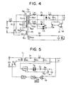
- a typical conventional multiple output type stabilizing power source apparatus as shown in Fig. 5 supplies a stabilized DC voltage to a DC load such as electronic equipment and a stabilized AC voltage to an AC load such as a fluorescent lamp.
- the stabilizing power source apparatus has inverters at the primary and secondary winding sides.
- a reference symbol V 0 denotes a DC voltage; Q 1 , a switching transistor; and T 1 , an inverter transformer.
- the inverter transformer T 1 has a primary winding Np and a secondary winding N s .
- Reference symbols D 1 and D 2 denote rectifying diodes, respectively; L 1 , a choke coil; and C 1 , a smoothing capacitor.
- a reference symbol A 1 denotes a differential amplifier for comparing a reference voltage V R with a DC output V 1 from the secondary winding N S and generating a signal corresponding to the difference.
- a reference symbol OSC denotes an oscillator for generating a triangular wave signal; and PWM, a pulse width modulator for converting the triangular wave from the oscillator OSC to pulses of the same frequency as that of the triangular wave and for changing a pulse width of the converted pulses in accordance with a shift of a crossing point between the triangular wave from the oscillator OSC and the signal from the differential amplifier A 1 .
- a reference symbol DR denotes a driver for amplifying the pulses from the pulse width modulator PWM and for supplying an amplified signal to the base of the transistor Q 1 .
- a reference symbol INV denotes an inverter for receiving the DC voltage V 1 from the secondary winding N S and for generating an AC voltage upon switching; T 2 , a voltage transformer for transforming the AC voltage from the inverter INV; C F , a waveshaping capacitor; and R L , an AC load for receiving an AC output V 2 .
- a resistor R S detects a current flowing through the AC load R L , and the inverter INV is switched to keep the current constant in response to the detection signal.
- a rectangular wave current obtained upon switching of the transistor Q 1 is rectified by the diodes D 1 and D 2 connected to the secondary winding N S .
- the rectified current is smoothed by the choke coil L 1 and the capacitor C 1 to provide the DC output V 1 .
- the DC output V 1 is supplied to the differential amplifier A 1 and is compared with the reference input voltage V R .
- the differential amplifier A 1 provides a signal corresponding to the difference to the pulse width modulator PWM.
- the pulse width modulator PWM the triangular wave from the oscillator OSC is converted to the pulses of the same frequency as that of the triangular wave.
- the pulse width is varied in accordance with the crossing point between the leading ramp of the triangular wave and the output from the differential amplifier A I .
- the pulse is amplified by the driver DR, and the amplified pulse is supplied to the base of the transistor Q 1 .
- the duty factor of the transistor Q 1 is thus controlled in response to the output from the differential amplifier A 1 . Therefore, the DC voltage V 1 is kept constant.
- the stabilized DC output V 1 is supplied to the inverter INV and is converted to the AC voltage upon its switching.
- the AC voltage is boosted by the transformer T 2 .
- the boosted voltage is then smoothed by the capacitor C F , and the smoothed output is supplied to the AC load R L .
- a stabilizing power source apparatus having a primary coil for receiving a DC voltage, a secondary coil magnetically coupled to the primary coil, and a switching element connected in series with the primary coil, the switching element being operated to turn on/off a current flowing through the primary coil so as to obtain a desired voltage output at the secondary coil, wherein the secondary coil is constituted by a first secondary coil and a second secondary coil, and the switching element is provided with a control input terminal for controlling switching thereof, and the apparatus comprises:
- a stabilizing power source apparatus having a first primary coil for receiving a DC voltage, a secondary coil magnetically coupled to the first primary coil, and a first switching element connected in series with the first primary coil, the first switching element being operated to turn on/off a current flowing through the first primary coil so as to obtain a desired voltage output at the secondary coil, wherein the first switching element has a control input terminal for controlling switching thereof, the secondary coil has at least first and second secondary coils, and the apparatus comprises:
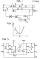
- Fig. 1 is a circuit diagram of a stabilizing power source apparatus according to an embodiment of the present invention.
- the same reference numerals as in Fig. 5 denote the same parts in Fig. 1.
- a reference symbol V 0 denotes an input DC voltage
- Q 1 a switching element
- T 3 an inverter transformer.
- the inverter transformer T 3 has a primary winding Np, a DC voltage output secondary winding N S1 magnetically coupled to the primary winding Np, and an AC output secondary winding N S2 magnetically coupled to the primary winding Np.
- the switching element Q 1 comprises a bipolar transistor but can be replaced with a GTO thyristor, a normal thyristor or the like.
- Reference symbols D 1 and D 2 denote rectifying diodes for the secondary winding N S1 ; L 1 , a choke coil; C 1 , a smoothing capacitor; L 2 , a choke coil for the secondary winding NS2 ; C 3 , a filter capacitor; R S , a resistor for detecting a load current; and R L , an AC load.
- a reference symbol A 1 denotes a differential amplifier for comparing a reference input voltage V R1 with the DC voltage from the secondary winding N S1 and generating a signal representing the difference therebetween.
- a reference symbol A 2 denotes a differential amplifier for receiving the AC voltage from the load current detecting resistor R S inserted between the secondary winding N S2 and the load R L , comparing the AC voltage with a reference input voltage V R2 and generating a signal representing the difference therebetween.
- a reference symbol OSC' denotes an oscillator for generating a triangular wave, the leading ramp of which is changed in response to the signal from the differential amplifier A 2 .
- a reference symbol PM denotes a pulse modulator for comparing the output signal from the differential amplifier A 1 with the triangular wave from the oscillator OSC' and generating a pulse, the width and frequency of which are changed in accordance with the shift of the crossing point between these input signals.
- a reference symbol DR denotes a driver for amplifying the pulse and supplying an amplified signal to the base of the transistor Q 1 .
- the duty factor of the transistor Q 1 is controlled to keep the DC output voltage V 1 constant.
- the switching frequency of the transistor Q 1 is controlled to keep the AC load current constant.
- Fig. 2 is a graph showing the relationship between input impedance Z and frequency f when the AC load R L is viewed from the secondary winding N S2 .
- the switching frequency f of the transistor Q 1 is decreased. Accordingly, the input impedance Z is increased and the load current is decreased (P 1 in Fig. 2).
- the switching frequency f of the transistor Q 1 is increased. Accordingly, the input impedance Z is increased, and the load current is also increased (P 2 in Fig. 2).
- the input impedance Z is given by:
- the resonant frequency f D is given by:
- Fig. 3 is a circuit diagram of the oscillator OSC' in the apparatus in Fig. 1.
- reference symbols R 11 to R 17 denote resistors; C 11 and C 12 , capacitors; Q 11 to Q 13' transistors; IC1, an integrated circuit element as a timer circuit; and IC 2 , an integrated circuit element as a NAND gate.
- the timer circuit IC 1 generates a clock signal with a period T at an output terminal OUT thereof so as to charge the capacitor C 11 in accordance with a time constant determined by the resistance of the resistor R 15 and the capacitance of the capacitor C 11 , and at the same time, discharge the capacitor C 11 in accordance with a time constant determined by the resistance of the resistor R17 and the capacitance of the capacitor C 11 .
- the clock signal is supplied to the base of the transistor Q 13 through the NAND gate IC 2 , so that the triangular wave voltage appears across the capacitor C 12 upon ON/OFF operation of the transistor Q 13'
- the triangular wave voltage signal is supplied from the collector of the transistor Q 13 to the pulse modulator PM.
- the transistor Q 11 When the AC voltage V 2 is constant and the signal from the differential amplifier A 2 is the reference voltage value, the transistor Q 11 is turned off.
- the timer circuit IC 1 generates the clock signal of a predetermined frequency.
- the internal resistance of the transistor Q 11 is decreased and the charge rate of the capacitor C 11 is increased. As a result, the period T of the clock signal is shortened.
- the internal resistance of the transistor Q 12 is decreased to increase the charge rate of the capacitor C 12 .
- the leading ramp of the triangular wave becomes steep. However, when the AC output V 2 is increased, the leading ramp of the triangular wave becomes moderate in the reverse process.
- the frequency of the oscillator OSC' varies in accordance with variations in the output signal from the differential amplifier A 2 which, in turn, varies in accordance with variations in that AC output V 2 0
- the width and frequency of the pulse supplied to the base of the switching transistor Q 1 vary in accordance with the variations in the voltage from the differential amplifier A. and the frequency of the triangular wave from the oscillator OSC'.
- the duty factor and the switching frequency of the transistor Q 1 are controlled to keep the DC voltage V 1 and the AC voltage V 2 constant.
- the inverter at the primary winding comprises a forward type inverter.
- the present invention is not limited to this arrangement.
- a half-bridge type inverter or a full-bridge type inverter can be used in place of the forward type inverter.
- the pulse width and frequency control circuit is exemplified by a PUM consisting of a variable frequency triangular wave oscillator and a comparator in the above description.
- the output signals from the two amplifiers can be supplied to an astable multivibrator to control the ON time intervals of transistors constituting the astable multivibrator. Therefore, the switching frequency and the ON time intervals can be simultaneously controlled.
- Fig. 4 is a circuit diagram of a stabilizing power source apparatus according to another embodiment of the present invention.
- the same reference numerals as in Fig. 1 denote the same parts in Fig. 4.
- a reference numeral V 0 denotes an input DC voltage
- L p a choke coil
- Q 2 and Q 3 switching transistors which are alternately turned on/off
- T 1 an inverter transformer.
- the inverter transformer T 1 has primary windings Np 1 and Np 2 .
- a reference symbol N D denotes a drive coil connected to the bases of the transistors Q 2 and Q 3 .
- a reference symbol Cp denotes a resonant capacitor inserted in parallel with the primary windings Np I and Np 2 .
- the switching transistors Q 2 and Q 3 comprise bipolar transistors, respectively, in the above arrangement, but can be replaced with other switching elements such as MOSFETs, GTO thyristors, normal thyristors.
- a waveshaper When thyristors are used, a waveshaper must be inserted between the coil N D and the two terminals of the switching element. In the case of thyristors, a commutating circuit must be added to turn off the thyristors.
- the above arrangement constitutes a resonant inverter for generating a sinusoidal wave voltage across the primary windings Np 1 and Np 2 .
- the switching operation of the two transistors is called push-pull operation.
- N S1 and N S2 denote secondary windings of the inverter transformer T 1 ; L S1 and L S2' saturable reactors connected in series with the secondary windings N S1 and NS2, respectively; D 1 , D 2 and D 3 , rectifying diodes; L 1 , a choke coil; and C 1 , a smoothing capacitor.
- N S3 denotes an AC output secondary winding
- C F a waveshaping capacitor
- R L an AC load
- a reference symbol A 1 denotes a differential amplifier for comparing a reference voltage V R with the DC voltage V 1 and generating a signal representing the difference therebetween.
- a reference symbol Q 4 denotes a transistor, the base of which is connected to the differential amplifier A. to receive the difference signal as a base current, the collector of which is connected to reactors L S1 and L S1 respectively through the saturable diodes D 4 and D 5 and the emitter of which is connected to the DC voltage V 1 .
- the transistor Q 4 comprises a bipolar transistor, but can be replaced' with another output current control element such as a MOSFFT.
- a voltage obtained by dividing the DC input voltage V 0 in accordance with the number of turns is induced at the drive coil N D magnetically coupled to the primary winding Np l .
- the base-emitter path of the transistor Q 3 is reverse-biased, and the transistor Q 3 is kept off.
- the voltage generated at the primary winding N P1 is a sinusoidal wave.
- a self-excited angular frequency w is given as: where L H is the inductance of the primary winding N P1 of the inverter transformer T 1 , C P ' is the capacitance for the primary winding N P1 based on the resonant capacitor Cp, and C F ' is the capacitance for the primary winding N P1 based on the waveshaping capacitor C F .
- the induction voltage at the drive coil N D which has been supplied as the reverse-bias voltage to the base of the transistor Q 3 is then forward-biased.
- the transistor Q 2 is now reverse-biased to turn on the transistor Q 3 and turn off the transistor Q 2 .
- the self-excited resonance is set in the negative half cycle.
- the transistors Q 2 and Q 3 are alternately turned on/off to generate the sinusoidal wave current at the primary windings N p1 and Np 2 .
- the current is then extracted at the secondary windings N S1 and N S2'
- the sinusoidal wave current is full-wave rectified by the diodes D 1 and D 3 .
- the rectified current is smoothed by the choke coil L 1 and the capacitor C 1 to provide the DC voltage V 1 .
- the DC voltage V 1 still varies in accordance with variations in the input DC voltage V 0 .
- the saturable reactors L S1 and L S2 are connected in series with the secondary windings N S1 and N S2 , respectively, thereby performing phase control.
- the saturable reactors are used to reduce noise at the secondary windings of the transformer.
- the saturable reactors serve as elements for controlling ON time of currents flowing through the coils and may be replaced with switching elements such as transistors.
- the saturable reactors L S1 and L S2 are arranged such that the phase control angles representing the present saturation timings are determined by the reset values of the magnetic flux. When the reset values are increased, the phase control angles are increased, and thus the output voltages are decreased.
- the DC voltage V 1 is compared by the differential amplifier A 1 with the reference input voltage V R , and the difference signal from the differential amplifier A 1 is supplied to the base of the transistor Q 4 .
- the collector of the transistor Q 4 is connected to the saturable reactors L S1 and LS2, the reset values of the saturable reactors L S1 and L S2 are controlled to cancel the variations in the DC voltage V 1 .
- the DC voltage V 1 is kept constant.
- the AC voltage from the secondary windings N S3 is supplied to the AC load R L through the waveshaping capacitor C F .
- the transistors Q 2 and Q 3 have conduction times.
- the transistors Q 2 and Q 3 are simultaneously turned on when the sinusoidal wave voltages at the primary windings N P1 and N p 2 are set to 0.
- the choke coil Lp is arranged at the DC input side to limit the short-circuiting current.
- the capacitor C F is used as the waveshaping element of the AC output secondary winding N S3 .
- a choke coil may be inserted in place of the capacitor C F .
- the self-excited angular frequency w' is given as: where L F ' is the inductance of the choke coil L F which is figured out on the basis of the primary winding N P1 , and Lp//L F ' is the total inductance of the inductance of the choke coil Lp and the inductance L F '.
- the sinusoidal wave voltage is applied in the collector-emitter paths of the transistors Q 2 and Q 3 , and the voltages at the transistors Q 2 and Q 3 are substantially zero at the turn on/off timing, thereby decreasing the switching loss.
- the line filter at the input side need not be large in size.
- the switching loss is decreased as described above, the switching frequency can be increased, and the inverter transformer T 1 can be made compact.
- the stabilizing power source apparatus has a single switching circuit, so that the number of components is decreased and the manufacturing cost is decreased.
- the apparatus is made small as a whole, and its reliability is improved.
- the sinusoidal wave is supplied to the primary windings, so that the conduction noise is decreased, and the circuit arrangement can be simplified.
- the transformer can be made compact and the apparatus as a whole can be made compact.
- the number of transformers can be decreased, and the insulated portion between the primary and secondary windings is decreased, thereby simplifying insulation design.
Landscapes
- Engineering & Computer Science (AREA)
- Power Engineering (AREA)
- Inverter Devices (AREA)
- Dc-Dc Converters (AREA)
Abstract
Description
- The present application claims priority of Japanese patent application Serial No. 59-277717 and 59-280922 filed on respective December 28, 1984 and December 29, 1985.
- The present invention relates to a multiple output type stabilizing power source apparatus for generating stabilized AC and DC voltages.
- A typical conventional multiple output type stabilizing power source apparatus as shown in Fig. 5 supplies a stabilized DC voltage to a DC load such as electronic equipment and a stabilized AC voltage to an AC load such as a fluorescent lamp.
- Referring to Fig. 5, the stabilizing power source apparatus has inverters at the primary and secondary winding sides. A reference symbol V0 denotes a DC voltage; Q1, a switching transistor; and T1, an inverter transformer. The inverter transformer T1 has a primary winding Np and a secondary winding Ns. Reference symbols D1 and D2 denote rectifying diodes, respectively; L1, a choke coil; and C1, a smoothing capacitor.
- A reference symbol A1 denotes a differential amplifier for comparing a reference voltage VR with a DC output V1 from the secondary winding NS and generating a signal corresponding to the difference. A reference symbol OSC denotes an oscillator for generating a triangular wave signal; and PWM, a pulse width modulator for converting the triangular wave from the oscillator OSC to pulses of the same frequency as that of the triangular wave and for changing a pulse width of the converted pulses in accordance with a shift of a crossing point between the triangular wave from the oscillator OSC and the signal from the differential amplifier A1. A reference symbol DR denotes a driver for amplifying the pulses from the pulse width modulator PWM and for supplying an amplified signal to the base of the transistor Q1.
- A reference symbol INV denotes an inverter for receiving the DC voltage V1 from the secondary winding NS and for generating an AC voltage upon switching; T2, a voltage transformer for transforming the AC voltage from the inverter INV; CF, a waveshaping capacitor; and RL, an AC load for receiving an AC output V2.
- It should be noted that a resistor RS detects a current flowing through the AC load RL, and the inverter INV is switched to keep the current constant in response to the detection signal.
- In the conventional stabilizing power source apparatus having the structure described above, a rectangular wave current obtained upon switching of the transistor Q1 is rectified by the diodes D1 and D2 connected to the secondary winding NS. The rectified current is smoothed by the choke coil L1 and the capacitor C1 to provide the DC output V1.
- The DC output V1 is supplied to the differential amplifier A1 and is compared with the reference input voltage VR. The differential amplifier A1 provides a signal corresponding to the difference to the pulse width modulator PWM.
- In the pulse width modulator PWM, the triangular wave from the oscillator OSC is converted to the pulses of the same frequency as that of the triangular wave. In this case, the pulse width is varied in accordance with the crossing point between the leading ramp of the triangular wave and the output from the differential amplifier AI. The pulse is amplified by the driver DR, and the amplified pulse is supplied to the base of the transistor Q1. The duty factor of the transistor Q1 is thus controlled in response to the output from the differential amplifier A1. Therefore, the DC voltage V1 is kept constant.
- On the other hand, the stabilized DC output V1 is supplied to the inverter INV and is converted to the AC voltage upon its switching. The AC voltage is boosted by the transformer T2. The boosted voltage is then smoothed by the capacitor CF, and the smoothed output is supplied to the AC load RL.
- When the AC load RL such as a discharge lamp is driven by the stabilizing power source apparatus described above, an AC voltage which is 3 to 5 times that in normal operation is required to start discharge. Since the capacitor CF is inserted at the output side of the transformer T2 and the output voltage at the transformer T2 drops to provide the normal operation voltage for the load RL, no voltage drop occurs across the capacitor CF at the start of discharge when no current flows through the load R. Thus, a high AC voltage is applied to the load RL.
- In the conventional stabilizing power source apparatus, however, since the switching circuits are arranged at the primary and secondary sides of the transformer, the circuit arrangement is complicated.
- Furthermore, since the rectangular wave voltage is supplied to the primary winding Np of the inverter transformer T1, an AC ripple is generated by capacitive couplings between the primary and secondary windings Np and NS. This ripple has the same phase as that of the normal signal component, so that the ripple is fed back to the primary winding Np through the ground line at the secondary winding N.0 Therefore, common mode noise including a comparatively high frequency component is generated.
- In the conventional apparatus of this type, a large line filter must be inserted at the input side to reduce such noise.
- It is an object of the present invention to provide a stabilizing power source apparatus with low-level common mode noise.
- It is another object of the present invention to provide a stabilizing power source apparatus which has a simple circuit structure and low manufacturing cost.
- According to an aspect of the present invention, there is provided a stabilizing power source apparatus having a primary coil for receiving a DC voltage, a secondary coil magnetically coupled to the primary coil, and a switching element connected in series with the primary coil, the switching element being operated to turn on/off a current flowing through the primary coil so as to obtain a desired voltage output at the secondary coil,
wherein the secondary coil is constituted by a first secondary coil and a second secondary coil, and the switching element is provided with a control input terminal for controlling switching thereof, and
the apparatus comprises: - a rectifying/smoothing circuit, connected to the first secondary coil, for generating a DC voltage;
- a first differential amplifier for comparing a first reference voltage with the DC voltage from the the rectifying/smoothing circuit, and for generating a difference signal representing a difference between the DC voltage and the first reference voltage;
- a second differential amplifier for comparing a second reference voltage with an AC voltage from the the second secondary coil, and for generating a difference signal representing a difference between the second reference voltage and the AC voltage;
- a pulse modulator for changing pulse width and frequency of a pulse in accordance with output signals from the first and second differential amplifiers; and
- a driver for amplifying the pulse and supplying an amplified signal to the control input terminal of the switching element, thereby controlling switching of the switching element.
- According to another aspect of the present invention, there is provided a stabilizing power source apparatus having a first primary coil for receiving a DC voltage, a secondary coil magnetically coupled to the first primary coil, and a first switching element connected in series with the first primary coil, the first switching element being operated to turn on/off a current flowing through the first primary coil so as to obtain a desired voltage output at the secondary coil,
wherein the first switching element has a control input terminal for controlling switching thereof, the secondary coil has at least first and second secondary coils, and
the apparatus comprises: - a drive coil magnetically coupled to the first primary coil and connected to the control input terminal of the first switching element;
- a differential amplifier for comparing a reference voltage with a DC voltage from the first secondary coil and generating a difference signal representing a difference between the DC voltage and the reference voltage;
- an ON time interval control circuit, connected to the first secondary coil, for controlling an ON time interval of the first secondary coil in response to an output signal from the differential amplifier;
- a rectifying/smoothing circuit for rectifying and smoothing an output from the ON time interval control circuit and generating the DC voltage; and
- a waveshaping element, connected in series with the second secondary coil, for generating an AC voltage.
-
- Fig. 1 is a circuit diagram of a stabilizing power source apparatus according to an embodiment of the present invention;
- Fig. 2 is a graph showing the relationship between the switching frequency and the input impedance;
- Fig. 3 is a circuit diagram of an oscillator OSC' in the apparatus in Fig. 1;
- Fig. 4 is a circuit diagram of a stabilizing power source apparatus according to another embodiment of the present invention; and
- Fig. 5 is a circuit diagram of a conventional stabilizing power source apparatus.
- Preferred embodiments of the present invention will be described in detail with reference to the accompanying drawings.
- Fig. 1 is a circuit diagram of a stabilizing power source apparatus according to an embodiment of the present invention. The same reference numerals as in Fig. 5 denote the same parts in Fig. 1.
- Referring to Fig. 1, a reference symbol V0 denotes an input DC voltage; Q1, a switching element; and T3, an inverter transformer. The inverter transformer T3 has a primary winding Np, a DC voltage output secondary winding NS1 magnetically coupled to the primary winding Np, and an AC output secondary winding NS2 magnetically coupled to the primary winding Np. In the above arrangement, the switching element Q1 comprises a bipolar transistor but can be replaced with a GTO thyristor, a normal thyristor or the like.
- Reference symbols D1 and D2 denote rectifying diodes for the secondary winding NS1; L1, a choke coil; C1, a smoothing capacitor; L2, a choke coil for the secondary winding NS2; C3, a filter capacitor; RS, a resistor for detecting a load current; and RL, an AC load.
- A reference symbol A1 denotes a differential amplifier for comparing a reference input voltage VR1 with the DC voltage from the secondary winding NS1 and generating a signal representing the difference therebetween. A reference symbol A2 denotes a differential amplifier for receiving the AC voltage from the load current detecting resistor RS inserted between the secondary winding NS2 and the load RL, comparing the AC voltage with a reference input voltage VR2 and generating a signal representing the difference therebetween. A reference symbol OSC' denotes an oscillator for generating a triangular wave, the leading ramp of which is changed in response to the signal from the differential amplifier A2. A reference symbol PM denotes a pulse modulator for comparing the output signal from the differential amplifier A1 with the triangular wave from the oscillator OSC' and generating a pulse, the width and frequency of which are changed in accordance with the shift of the crossing point between these input signals. A reference symbol DR denotes a driver for amplifying the pulse and supplying an amplified signal to the base of the transistor Q1.
- In the stabilizing power source apparatus having the arrangement described above, the duty factor of the transistor Q1 is controlled to keep the DC output voltage V1 constant. At the same time, the switching frequency of the transistor Q1 is controlled to keep the AC load current constant.
- The operation of the stabilizing power source apparatus will be described in detail hereinafter.
- Fig. 2 is a graph showing the relationship between input impedance Z and frequency f when the AC load RL is viewed from the secondary winding NS2.
- When the AC load RL comprises a light load, the switching frequency f of the transistor Q1 is decreased. Accordingly, the input impedance Z is increased and the load current is decreased (P1 in Fig. 2).
- However, when the AC load RL comprises a heavy load, the switching frequency f of the transistor Q1 is increased. Accordingly, the input impedance Z is increased, and the load current is also increased (P2 in Fig. 2).
- The input impedance Z is given by:

- The resonant frequency fD is given by:

- When the load current is increased in the apparatus in Fig. 1, the voltage input to the differential amplifier A2 is increased, and hence the voltage output from the differential amplifier A2 is increased. In response to an increase in output voltage, the oscillation frequency of the oscillator OSC' is decreased, but the input impedance Z is increased. As a result, the load current is decreased. Therefore, the current flowing through the load current is always kept constant.
- Fig. 3 is a circuit diagram of the oscillator OSC' in the apparatus in Fig. 1.
- Referring to Fig. 3, reference symbols R11 to R 17 denote resistors; C11 and C12, capacitors; Q11 to Q13' transistors; IC1, an integrated circuit element as a timer circuit; and IC2, an integrated circuit element as a NAND gate.
- In the oscillator OSC' described above, the timer circuit IC1 generates a clock signal with a period T at an output terminal OUT thereof so as to charge the capacitor C11 in accordance with a time constant determined by the resistance of the resistor R15 and the capacitance of the capacitor C11, and at the same time, discharge the capacitor C11 in accordance with a time constant determined by the resistance of the resistor R17 and the capacitance of the capacitor C11.
- The clock signal is supplied to the base of the transistor Q13 through the NAND gate IC2, so that the triangular wave voltage appears across the capacitor C12 upon ON/OFF operation of the transistor Q13'
- The triangular wave voltage signal is supplied from the collector of the transistor Q13 to the pulse modulator PM.
- When the AC voltage V2 is constant and the signal from the differential amplifier A2 is the reference voltage value, the transistor Q11 is turned off. The timer circuit IC1 generates the clock signal of a predetermined frequency. However, when the AC output V2 is decreased and then the signal voltage from the differential amplifier A2 is decreased, the internal resistance of the transistor Q11 is decreased and the charge rate of the capacitor C11 is increased. As a result, the period T of the clock signal is shortened.
- Upon shortening of the period T, the internal resistance of the transistor Q12 is decreased to increase the charge rate of the capacitor C12. The leading ramp of the triangular wave becomes steep. However, when the AC output V2 is increased, the leading ramp of the triangular wave becomes moderate in the reverse process.
- The frequency of the oscillator OSC' varies in accordance with variations in the output signal from the differential amplifier A2 which, in turn, varies in accordance with variations in that
AC output V 20 - In the pulse modulator PM, the width and frequency of the pulse supplied to the base of the switching transistor Q1 vary in accordance with the variations in the voltage from the differential amplifier A. and the frequency of the triangular wave from the oscillator OSC'. The duty factor and the switching frequency of the transistor Q1 are controlled to keep the DC voltage V1 and the AC voltage V2 constant.
- In the above embodiment, the inverter at the primary winding comprises a forward type inverter. However, the present invention is not limited to this arrangement. A half-bridge type inverter or a full-bridge type inverter can be used in place of the forward type inverter.
- The pulse width and frequency control circuit is exemplified by a PUM consisting of a variable frequency triangular wave oscillator and a comparator in the above description. Alternatively, the output signals from the two amplifiers can be supplied to an astable multivibrator to control the ON time intervals of transistors constituting the astable multivibrator. Therefore, the switching frequency and the ON time intervals can be simultaneously controlled.
- Fig. 4 is a circuit diagram of a stabilizing power source apparatus according to another embodiment of the present invention. The same reference numerals as in Fig. 1 denote the same parts in Fig. 4.
- Referring to Fig. 4, a reference numeral V0 denotes an input DC voltage; Lp, a choke coil; Q2 and Q3, switching transistors which are alternately turned on/off; and T1, an inverter transformer. The inverter transformer T1 has primary windings Np1 and Np2. A reference symbol ND denotes a drive coil connected to the bases of the transistors Q2 and Q3. A reference symbol Cp denotes a resonant capacitor inserted in parallel with the primary windings NpI and Np2. The switching transistors Q2 and Q3 comprise bipolar transistors, respectively, in the above arrangement, but can be replaced with other switching elements such as MOSFETs, GTO thyristors, normal thyristors. When thyristors are used, a waveshaper must be inserted between the coil ND and the two terminals of the switching element. In the case of thyristors, a commutating circuit must be added to turn off the thyristors.
- The above arrangement constitutes a resonant inverter for generating a sinusoidal wave voltage across the primary windings Np1 and Np2.
- The switching operation of the two transistors is called push-pull operation.
- A reference symbols NS1 and NS2 denote secondary windings of the inverter transformer T1; LS1 and LS2' saturable reactors connected in series with the secondary windings NS1 and NS2, respectively; D1, D2 and D3, rectifying diodes; L1, a choke coil; and C1, a smoothing capacitor.
- A reference symbol NS3 denotes an AC output secondary winding; CF, a waveshaping capacitor; and RL, an AC load.
- A reference symbol A1 denotes a differential amplifier for comparing a reference voltage VR with the DC voltage V1 and generating a signal representing the difference therebetween. A reference symbol Q4 denotes a transistor, the base of which is connected to the differential amplifier A. to receive the difference signal as a base current, the collector of which is connected to reactors LS1 and LS1 respectively through the saturable diodes D4 and D5 and the emitter of which is connected to the DC voltage V1. The transistor Q4 comprises a bipolar transistor, but can be replaced' with another output current control element such as a MOSFFT.
- The operation of the stabilizing power source apparatus having the arrangement described above will be described hereinafter.
- When the input DC voltage V0 is supplied to the apparatus, a current flows in the bases of the transistors Q2 and Q3 through the resistors R1 and R2, so that one of the
transistors - Assume that the transistor Q2 is turned on first and the voltage V0 is supplied to the primary winding NP1 of the inverter transformer T1.
- In this case, a voltage obtained by dividing the DC input voltage V0 in accordance with the number of turns is induced at the drive coil ND magnetically coupled to the primary winding Npl. The base-emitter path of the transistor Q3 is reverse-biased, and the transistor Q3 is kept off. In this case, the voltage generated at the primary winding NP1 is a sinusoidal wave.
- A self-excited angular frequency w is given as:

where LH is the inductance of the primary winding NP1 of the inverter transformer T1, CP' is the capacitance for the primary winding NP1 based on the resonant capacitor Cp, and CF' is the capacitance for the primary winding NP1 based on the waveshaping capacitor CF. - When the sinusoidal wave voltage at the primary winding NP1 transits to the negative polarity through a zero-crossing point, the induction voltage at the drive coil ND changes likewise.
- The induction voltage at the drive coil ND which has been supplied as the reverse-bias voltage to the base of the transistor Q3 is then forward-biased. The transistor Q2 is now reverse-biased to turn on the transistor Q3 and turn off the transistor Q2. As a result, the self-excited resonance is set in the negative half cycle.
- The transistors Q2 and Q3 are alternately turned on/off to generate the sinusoidal wave current at the primary windings Np1 and Np2. The current is then extracted at the secondary windings NS1 and NS2'
- If the saturable reactors LS1 and LS2 are not arranged, the sinusoidal wave current is full-wave rectified by the diodes D1 and D3. The rectified current is smoothed by the choke coil L1 and the capacitor C1 to provide the DC voltage V1. In this case, the DC voltage V1 still varies in accordance with variations in the input DC voltage V0.
- In order to stabilize the output voltage V1, the saturable reactors LS1 and LS2 are connected in series with the secondary windings NS1 and NS2, respectively, thereby performing phase control.
- In this embodiment, the saturable reactors are used to reduce noise at the secondary windings of the transformer. The saturable reactors serve as elements for controlling ON time of currents flowing through the coils and may be replaced with switching elements such as transistors.
- The saturable reactors LS1 and LS2 are arranged such that the phase control angles representing the present saturation timings are determined by the reset values of the magnetic flux. When the reset values are increased, the phase control angles are increased, and thus the output voltages are decreased.
- The DC voltage V1 is compared by the differential amplifier A1 with the reference input voltage VR, and the difference signal from the differential amplifier A1 is supplied to the base of the transistor Q4. In this case, since the collector of the transistor Q4 is connected to the saturable reactors LS1 and LS2, the reset values of the saturable reactors LS1 and LS2 are controlled to cancel the variations in the DC voltage V1.
- The DC voltage V1 is kept constant.
- The AC voltage from the secondary windings NS3 is supplied to the AC load RL through the waveshaping capacitor CF.
- The transistors Q2 and Q3 have conduction times. The transistors Q2 and Q3 are simultaneously turned on when the sinusoidal wave voltages at the primary windings NP1 and Np2 are set to 0. In this case, the choke coil Lp is arranged at the DC input side to limit the short-circuiting current.
- In the above embodiment, the capacitor CF is used as the waveshaping element of the AC output secondary winding NS3. However, a choke coil may be inserted in place of the capacitor CF.
- In this case, the self-excited angular frequency w' is given as:

where LF' is the inductance of the choke coil LF which is figured out on the basis of the primary winding NP1, and Lp//LF' is the total inductance of the inductance of the choke coil Lp and the inductance LF'. - In the stabilizing power source apparatus described above, the sinusoidal wave voltage is applied in the collector-emitter paths of the transistors Q2 and Q3, and the voltages at the transistors Q2 and Q3 are substantially zero at the turn on/off timing, thereby decreasing the switching loss.
- Since the sinusoidal wave signal is supplied to the primary winding of the inverter transformer T1, only low-level harmonic waves are generated as compared with the case wherein a rectangular wave voltage is supplied to the primary winding of the inverter transformer T1.
- Since the common mode AC current flowing in the secondary windings through the coupling capacitance CS between the primary and secondary windings is decreased, the line filter at the input side need not be large in size.
- Since the switching loss is decreased as described above, the switching frequency can be increased, and the inverter transformer T1 can be made compact.
- According to the present invention, the stabilizing power source apparatus has a single switching circuit, so that the number of components is decreased and the manufacturing cost is decreased. In addition, the apparatus is made small as a whole, and its reliability is improved.
- According to the present invention, the sinusoidal wave is supplied to the primary windings, so that the conduction noise is decreased, and the circuit arrangement can be simplified.
- Furthermore, since the switching frequency can be increased, the transformer can be made compact and the apparatus as a whole can be made compact.
- The number of transformers can be decreased, and the insulated portion between the primary and secondary windings is decreased, thereby simplifying insulation design.
Claims (9)
characterized in that said secondary coil (NS) is constituted by a first secondary coil (NS1) and a second secondary coil (NS2), and said switching element (Q1) is provided with a control input terminal for controlling switching thereof, and
said apparatus comprises:
characterized in that said first switching element (Q2, Q3) has a control input terminal for controlling switching thereof, said secondary coil (NS) has at least first and second secondary coils (NS1, NS2; NS3) and
said apparatus comprises:
Priority Applications (1)
| Application Number | Priority Date | Filing Date | Title |
|---|---|---|---|
| EP91202705A EP0471421B1 (en) | 1984-12-28 | 1985-12-30 | Stabilizing power source apparatus |
Applications Claiming Priority (4)
| Application Number | Priority Date | Filing Date | Title |
|---|---|---|---|
| JP277717/84 | 1984-12-28 | ||
| JP27771784A JPS61157263A (en) | 1984-12-28 | 1984-12-28 | Stabilized power source |
| JP280922/84 | 1984-12-29 | ||
| JP28092284A JPS61161964A (en) | 1984-12-29 | 1984-12-29 | Stabilized power source |
Related Child Applications (1)
| Application Number | Title | Priority Date | Filing Date |
|---|---|---|---|
| EP91202705.9 Division-Into | 1991-10-18 |
Publications (3)
| Publication Number | Publication Date |
|---|---|
| EP0189680A2 true EP0189680A2 (en) | 1986-08-06 |
| EP0189680A3 EP0189680A3 (en) | 1988-03-16 |
| EP0189680B1 EP0189680B1 (en) | 1993-02-10 |
Family
ID=26552531
Family Applications (2)
| Application Number | Title | Priority Date | Filing Date |
|---|---|---|---|
| EP91202705A Expired - Lifetime EP0471421B1 (en) | 1984-12-28 | 1985-12-30 | Stabilizing power source apparatus |
| EP85309536A Expired - Lifetime EP0189680B1 (en) | 1984-12-28 | 1985-12-30 | Stabilizing power source apparatus |
Family Applications Before (1)
| Application Number | Title | Priority Date | Filing Date |
|---|---|---|---|
| EP91202705A Expired - Lifetime EP0471421B1 (en) | 1984-12-28 | 1985-12-30 | Stabilizing power source apparatus |
Country Status (3)
| Country | Link |
|---|---|
| US (1) | US4677534A (en) |
| EP (2) | EP0471421B1 (en) |
| DE (2) | DE3587090T2 (en) |
Cited By (6)
| Publication number | Priority date | Publication date | Assignee | Title |
|---|---|---|---|---|
| EP0240312A2 (en) * | 1986-03-31 | 1987-10-07 | Kabushiki Kaisha Toshiba | Stabilized electric power apparatus for generating direct and alternating current simultaneously in one transformer |
| EP0355415A2 (en) * | 1988-08-26 | 1990-02-28 | ANT Nachrichtentechnik GmbH | Switching regulator |
| EP0498651A2 (en) * | 1991-02-08 | 1992-08-12 | General Electric Company | High power factor power supply |
| EP0564413A2 (en) * | 1992-02-28 | 1993-10-06 | Canon Kabushiki Kaisha | Image forming apparatus copying with power supply voltage drift |
| WO2009070086A1 (en) * | 2007-11-27 | 2009-06-04 | Milux Holding Sa | Energy transfer control adapted to a medical device system |
| EP2200164A1 (en) * | 2007-09-26 | 2010-06-23 | Huawei Technologies Co., Ltd. | Direct current converter power supply apparatus and method for improving direct current converter power supply apparatus |
Families Citing this family (56)
| Publication number | Priority date | Publication date | Assignee | Title |
|---|---|---|---|---|
| US4772995A (en) * | 1987-01-08 | 1988-09-20 | Veeco Instruments Inc. | Switching supply with pulse width and rate modulation |
| US4855885A (en) * | 1988-04-11 | 1989-08-08 | Dsl Dynamic Sciences Limited | Light beam intensifier |
| US4893227A (en) * | 1988-07-08 | 1990-01-09 | Venus Scientific, Inc. | Push pull resonant flyback switchmode power supply converter |
| CA1316980C (en) * | 1988-12-27 | 1993-04-27 | Daniel C. Hughey | Power supply |
| US5128593A (en) * | 1990-01-25 | 1992-07-07 | Beckman Instruments, Inc. | Power supply for gas-filled lamps |
| US5448469A (en) * | 1990-02-15 | 1995-09-05 | Deutsche Thomson-Brandt Gmbh | Switch mode power supply with output feedback isolation |
| US5231563A (en) * | 1990-09-07 | 1993-07-27 | Itt Corporation | Square wave converter having an improved zero voltage switching operation |
| US5126931A (en) * | 1990-09-07 | 1992-06-30 | Itt Corporation | Fixed frequency single ended forward converter switching at zero voltage |
| US5084666A (en) * | 1990-10-23 | 1992-01-28 | International Business Machines Corporation | Switchable output voltage converter |
| US5132889A (en) * | 1991-05-15 | 1992-07-21 | Ibm Corporation | Resonant-transition DC-to-DC converter |
| US5285367A (en) * | 1992-02-07 | 1994-02-08 | Power Integrations, Inc. | Linear load circuit to control switching power supplies under minimum load conditions |
| GB9214896D0 (en) * | 1992-07-14 | 1992-08-26 | Attwood Brian E | A low cost 1mhz ferrite regulated converter |
| US5479087A (en) * | 1992-10-02 | 1995-12-26 | Compaq Computer Corp. | Synchronized switch tapped coupled inductor regulation circuit |
| EP0689731A1 (en) * | 1993-03-17 | 1996-01-03 | National Semiconductor Corporation | Frequency shift circuit for switching regulator |
| JP2758552B2 (en) * | 1993-08-27 | 1998-05-28 | 浜松ホトニクス株式会社 | Push-pull resonant switching power supply circuit |
| US5640315A (en) * | 1994-03-18 | 1997-06-17 | Nippon Steel Corporation | Switching regulator |
| DE4424800A1 (en) * | 1994-07-14 | 1996-01-18 | Philips Patentverwaltung | Circuit arrangement for supplying supply voltages |
| KR0150384B1 (en) * | 1995-05-31 | 1998-10-15 | 배순훈 | High voltage stabilization circuit |
| US5702431A (en) * | 1995-06-07 | 1997-12-30 | Sulzer Intermedics Inc. | Enhanced transcutaneous recharging system for battery powered implantable medical device |
| US5690693A (en) * | 1995-06-07 | 1997-11-25 | Sulzer Intermedics Inc. | Transcutaneous energy transmission circuit for implantable medical device |
| US5745358A (en) * | 1996-05-01 | 1998-04-28 | Compaq Computer Corporation | Variable-frequency converter with constant programmed delay |
| US5973939A (en) * | 1996-08-29 | 1999-10-26 | Trw Inc. | Double forward converter with soft-PWM switching |
| US7269034B2 (en) | 1997-01-24 | 2007-09-11 | Synqor, Inc. | High efficiency power converter |
| US6130509A (en) * | 1999-01-22 | 2000-10-10 | Dell Computer Corporation | Balanced feedback system for floating cold cathode fluorescent lamps |
| US6471635B1 (en) | 2000-02-10 | 2002-10-29 | Obtech Medical Ag | Anal incontinence disease treatment with controlled wireless energy supply |
| US6482145B1 (en) | 2000-02-14 | 2002-11-19 | Obtech Medical Ag | Hydraulic anal incontinence treatment |
| US6461292B1 (en) | 1999-08-12 | 2002-10-08 | Obtech Medical Ag | Anal incontinence treatment with wireless energy supply |
| US6464628B1 (en) | 1999-08-12 | 2002-10-15 | Obtech Medical Ag | Mechanical anal incontinence |
| DE60113965T2 (en) * | 2000-02-10 | 2006-07-06 | Potencia Medical Ag | TREATMENT OF HARNINE CONTINENCE WITH WIRELESS ENERGY SUPPLY |
| CA2695722C (en) | 2000-02-10 | 2015-04-21 | Urologica Ag | Controlled urinary incontinence treatment |
| DE60133592T2 (en) | 2000-02-10 | 2009-04-30 | Potencia Medical Ag | Mechanical device for impotence treatment |
| US20030125768A1 (en) | 2000-02-11 | 2003-07-03 | Forsell Peter | Impotence treatment apparatus with energy transforming means |
| ATE296071T1 (en) | 2000-02-14 | 2005-06-15 | Potencia Medical Ag | PENIS PROSTHESIS |
| BR0108307B1 (en) | 2000-02-14 | 2009-12-01 | Prosthesis apparatus for the treatment of male sexual impotence with wireless power supply device. | |
| US20030100929A1 (en) | 2000-02-14 | 2003-05-29 | Peter Forsell | Controlled penile prosthesis |
| KR100369834B1 (en) * | 2000-12-27 | 2003-01-30 | 삼성전자 주식회사 | Power controlling system and method for display |
| DE60140421D1 (en) * | 2001-01-22 | 2009-12-24 | St Microelectronics Srl | Switching Power Supply |
| DE10122534A1 (en) * | 2001-05-09 | 2002-11-21 | Philips Corp Intellectual Pty | Resonant converter |
| EP1257048B1 (en) * | 2001-05-09 | 2017-10-04 | Philips Lighting Holding B.V. | Regulation device for a resonant converter |
| EP2092800A1 (en) * | 2006-12-21 | 2009-08-26 | Osram Gesellschaft mit Beschränkter Haftung | A cell arrangement for feeding electrical loads such as light sources, corresponding circuit and design method |
| US7764517B2 (en) * | 2007-11-02 | 2010-07-27 | National Semiconductor Corporation | Power supply with reduced power consumption when a load is disconnected from the power supply |
| AU2009209518A1 (en) * | 2008-01-28 | 2009-08-06 | Milux Holding S.A. | A drainage device comprising an active filter |
| CN105997315B (en) | 2008-01-29 | 2019-03-15 | 米卢克斯控股股份有限公司 | For treating the devices, systems, and methods of obesity |
| US7983059B2 (en) * | 2008-09-02 | 2011-07-19 | Analog Devices, Inc. | High frequency power converter based on transformers |
| EP3851076A1 (en) | 2008-10-10 | 2021-07-21 | MedicalTree Patent Ltd. | An improved artificial valve |
| EP3120896A1 (en) | 2008-10-10 | 2017-01-25 | Kirk Promotion LTD. | A system, an apparatus, and a method for treating a sexual dysfunctional female patient |
| CN105079898B (en) | 2008-10-10 | 2018-12-14 | 米卢克斯控股股份有限公司 | Heart-assist device, system and method |
| WO2010042012A1 (en) | 2008-10-10 | 2010-04-15 | Milux Holding Sa | Heart help device, system, and method |
| WO2010042032A1 (en) * | 2008-10-10 | 2010-04-15 | Milux Holding S.A. | Fastening means for implantable medcial control assembly |
| ES2962384T3 (en) | 2008-10-10 | 2024-03-18 | Implantica Patent Ltd | Device for the treatment of female sexual dysfunction |
| US8149600B2 (en) * | 2009-05-22 | 2012-04-03 | Infineon Technologies Ag | System and method for ringing suppression in a switched mode power supply |
| US10952836B2 (en) | 2009-07-17 | 2021-03-23 | Peter Forsell | Vaginal operation method for the treatment of urinary incontinence in women |
| US9949812B2 (en) | 2009-07-17 | 2018-04-24 | Peter Forsell | Vaginal operation method for the treatment of anal incontinence in women |
| US9293997B2 (en) | 2013-03-14 | 2016-03-22 | Analog Devices Global | Isolated error amplifier for isolated power supplies |
| US10199950B1 (en) | 2013-07-02 | 2019-02-05 | Vlt, Inc. | Power distribution architecture with series-connected bus converter |
| JP2022148109A (en) | 2021-03-24 | 2022-10-06 | スミダコーポレーション株式会社 | Output stabilizing circuit and dc/dc converter circuit |
Citations (3)
| Publication number | Priority date | Publication date | Assignee | Title |
|---|---|---|---|---|
| US3818306A (en) * | 1972-02-18 | 1974-06-18 | Sits Soc It Telecom Siemens | Stabilized power supply with transformer isolation |
| US3843919A (en) * | 1972-07-20 | 1974-10-22 | Nippon Telegraph & Telephone | Dc-to-dc converter |
| US4322817A (en) * | 1980-12-29 | 1982-03-30 | Gte Automatic Electric Labs Inc. | Switching regulated pulse width modulated push-pull converter |
Family Cites Families (6)
| Publication number | Priority date | Publication date | Assignee | Title |
|---|---|---|---|---|
| NL7101662A (en) * | 1971-02-09 | 1972-08-11 | ||
| DE3008887C2 (en) * | 1980-03-07 | 1982-06-24 | Siemens AG, 1000 Berlin und 8000 München | Push-pull converter with a saturable transformer |
| US4451876A (en) * | 1981-06-19 | 1984-05-29 | Hitachi Metals, Ltd. | Switching regulator |
| NL8105160A (en) * | 1981-11-16 | 1983-06-16 | Philips Nv | CIRCUIT FOR CONVERTING AN INPUT DC VOLTAGE TO AN OUTPUT DC VOLTAGE. |
| DE3209975A1 (en) * | 1982-03-18 | 1983-09-29 | Nixdorf Computer Ag, 4790 Paderborn | Circuit arrangement for controlling the magnitude of a pulsating voltage which is to be emitted, especially in a DC converter |
| US4535399A (en) * | 1983-06-03 | 1985-08-13 | National Semiconductor Corporation | Regulated switched power circuit with resonant load |
-
1985
- 1985-12-30 EP EP91202705A patent/EP0471421B1/en not_active Expired - Lifetime
- 1985-12-30 EP EP85309536A patent/EP0189680B1/en not_active Expired - Lifetime
- 1985-12-30 US US06/814,494 patent/US4677534A/en not_active Expired - Fee Related
- 1985-12-30 DE DE8585309536T patent/DE3587090T2/en not_active Expired - Fee Related
- 1985-12-30 DE DE3588108T patent/DE3588108T2/en not_active Expired - Fee Related
Patent Citations (3)
| Publication number | Priority date | Publication date | Assignee | Title |
|---|---|---|---|---|
| US3818306A (en) * | 1972-02-18 | 1974-06-18 | Sits Soc It Telecom Siemens | Stabilized power supply with transformer isolation |
| US3843919A (en) * | 1972-07-20 | 1974-10-22 | Nippon Telegraph & Telephone | Dc-to-dc converter |
| US4322817A (en) * | 1980-12-29 | 1982-03-30 | Gte Automatic Electric Labs Inc. | Switching regulated pulse width modulated push-pull converter |
Non-Patent Citations (2)
| Title |
|---|
| 17TH ANNUAL IEEE POWER ELECTRONICS SPECIALISTS CONFERENCE 1986, pages 367-374, IEEE, New York, US; T. NINOMIYA et al.: "Analysis of the static and dynamic characteristics of push-pull parallel resonant converters" * |
| RADIO FERNSEHEN ELEKTRONIK, vol. 30, no. 6, 1981, page 403, Berlin, DE; "Gleichspannungswandler mit zwei geregelten Ausgangsspannungen" * |
Cited By (12)
| Publication number | Priority date | Publication date | Assignee | Title |
|---|---|---|---|---|
| EP0240312A2 (en) * | 1986-03-31 | 1987-10-07 | Kabushiki Kaisha Toshiba | Stabilized electric power apparatus for generating direct and alternating current simultaneously in one transformer |
| EP0240312A3 (en) * | 1986-03-31 | 1989-07-26 | Kabushiki Kaisha Toshiba | Stabilized electric power apparatus for generating direct and alternating current simultaneously in one transformer |
| EP0355415A2 (en) * | 1988-08-26 | 1990-02-28 | ANT Nachrichtentechnik GmbH | Switching regulator |
| EP0355415A3 (en) * | 1988-08-26 | 1990-08-16 | Ant Nachrichtentechnik Gmbh | Switching regulator |
| EP0498651A2 (en) * | 1991-02-08 | 1992-08-12 | General Electric Company | High power factor power supply |
| EP0498651A3 (en) * | 1991-02-08 | 1992-10-14 | General Electric Company | High power factor power supply |
| EP0564413A2 (en) * | 1992-02-28 | 1993-10-06 | Canon Kabushiki Kaisha | Image forming apparatus copying with power supply voltage drift |
| EP0564413A3 (en) * | 1992-02-28 | 1995-08-23 | Canon Kk | Image forming apparatus copying with power supply voltage drift |
| EP2200164A1 (en) * | 2007-09-26 | 2010-06-23 | Huawei Technologies Co., Ltd. | Direct current converter power supply apparatus and method for improving direct current converter power supply apparatus |
| EP2200164A4 (en) * | 2007-09-26 | 2010-09-22 | Huawei Tech Co Ltd | Direct current converter power supply apparatus and method for improving direct current converter power supply apparatus |
| WO2009070086A1 (en) * | 2007-11-27 | 2009-06-04 | Milux Holding Sa | Energy transfer control adapted to a medical device system |
| US8600517B2 (en) | 2007-11-27 | 2013-12-03 | Peter Forsell | Energy transfer control adapted to a medical device system |
Also Published As
| Publication number | Publication date |
|---|---|
| EP0471421A2 (en) | 1992-02-19 |
| DE3588108D1 (en) | 1996-06-27 |
| EP0189680A3 (en) | 1988-03-16 |
| EP0471421B1 (en) | 1996-05-22 |
| DE3587090T2 (en) | 1993-06-03 |
| DE3588108T2 (en) | 1996-11-07 |
| US4677534A (en) | 1987-06-30 |
| DE3587090D1 (en) | 1993-03-25 |
| EP0471421A3 (en) | 1993-02-03 |
| EP0189680B1 (en) | 1993-02-10 |
Similar Documents
| Publication | Publication Date | Title |
|---|---|---|
| US4677534A (en) | Stabilizing power source apparatus | |
| EP0444428B1 (en) | PWM-controlled power supply including choke coil with 3 windings | |
| US5223767A (en) | Low harmonic compact fluorescent lamp ballast | |
| JP3531385B2 (en) | Power supply | |
| JP3443654B2 (en) | Voltage resonance type inverter circuit | |
| JP2003520407A (en) | Power feedback power factor correction scheme for multiple lamp operation. | |
| EP0240312A2 (en) | Stabilized electric power apparatus for generating direct and alternating current simultaneously in one transformer | |
| JPH09131051A (en) | Power factor improving converter circuit | |
| US5563775A (en) | Full bridge phase displaced resonant transition circuit for obtaining constant resonant transition current from 0° phase angle to 180° phase angle | |
| JP3312369B2 (en) | Inverter device | |
| JP3371595B2 (en) | Current resonance type switching power supply | |
| JPS59191485A (en) | Low loss high frequency inverter | |
| JPH05304772A (en) | Power supply circuit | |
| JP3211380B2 (en) | Power converter | |
| JP3259337B2 (en) | Power converter | |
| KR920000361B1 (en) | High efficiency driver circuit for ringing converter | |
| WO2002039570A1 (en) | Switching mode power supply | |
| JPS61277372A (en) | Power supply device | |
| JP2628204B2 (en) | Driving method of series resonant converter | |
| JP3492779B2 (en) | Power supply | |
| JP3277551B2 (en) | Power circuit | |
| JPS5923186B2 (en) | switching power supply circuit | |
| JP3316314B2 (en) | Power supply | |
| KR100270944B1 (en) | Ballast circuit | |
| JP2690418B2 (en) | Power supply |
Legal Events
| Date | Code | Title | Description |
|---|---|---|---|
| PUAI | Public reference made under article 153(3) epc to a published international application that has entered the european phase |
Free format text: ORIGINAL CODE: 0009012 |
|
| 17P | Request for examination filed |
Effective date: 19860109 |
|
| AK | Designated contracting states |
Kind code of ref document: A2 Designated state(s): DE FR GB IT NL |
|
| PUAL | Search report despatched |
Free format text: ORIGINAL CODE: 0009013 |
|
| AK | Designated contracting states |
Kind code of ref document: A3 Designated state(s): DE FR GB IT NL |
|
| 17Q | First examination report despatched |
Effective date: 19900817 |
|
| GRAA | (expected) grant |
Free format text: ORIGINAL CODE: 0009210 |
|
| AK | Designated contracting states |
Kind code of ref document: B1 Designated state(s): DE FR GB IT NL |
|
| XX | Miscellaneous (additional remarks) |
Free format text: TEILANMELDUNG 91202705.9 EINGEREICHT AM 30/12/85. |
|
| ITF | It: translation for a ep patent filed |
Owner name: BUGNION S.P.A. |
|
| XX | Miscellaneous (additional remarks) | ||
| REF | Corresponds to: |
Ref document number: 3587090 Country of ref document: DE Date of ref document: 19930325 |
|
| ET | Fr: translation filed | ||
| PLBE | No opposition filed within time limit |
Free format text: ORIGINAL CODE: 0009261 |
|
| STAA | Information on the status of an ep patent application or granted ep patent |
Free format text: STATUS: NO OPPOSITION FILED WITHIN TIME LIMIT |
|
| 26N | No opposition filed | ||
| PGFP | Annual fee paid to national office [announced via postgrant information from national office to epo] |
Ref country code: FR Payment date: 19961211 Year of fee payment: 12 |
|
| PGFP | Annual fee paid to national office [announced via postgrant information from national office to epo] |
Ref country code: GB Payment date: 19961223 Year of fee payment: 12 |
|
| PGFP | Annual fee paid to national office [announced via postgrant information from national office to epo] |
Ref country code: NL Payment date: 19961231 Year of fee payment: 12 |
|
| PGFP | Annual fee paid to national office [announced via postgrant information from national office to epo] |
Ref country code: DE Payment date: 19970107 Year of fee payment: 12 |
|
| PG25 | Lapsed in a contracting state [announced via postgrant information from national office to epo] |
Ref country code: GB Free format text: LAPSE BECAUSE OF NON-PAYMENT OF DUE FEES Effective date: 19971230 |
|
| PG25 | Lapsed in a contracting state [announced via postgrant information from national office to epo] |
Ref country code: FR Free format text: THE PATENT HAS BEEN ANNULLED BY A DECISION OF A NATIONAL AUTHORITY Effective date: 19971231 |
|
| PG25 | Lapsed in a contracting state [announced via postgrant information from national office to epo] |
Ref country code: NL Free format text: LAPSE BECAUSE OF NON-PAYMENT OF DUE FEES Effective date: 19980701 |
|
| GBPC | Gb: european patent ceased through non-payment of renewal fee |
Effective date: 19971230 |
|
| NLV4 | Nl: lapsed or anulled due to non-payment of the annual fee |
Effective date: 19980701 |
|
| PG25 | Lapsed in a contracting state [announced via postgrant information from national office to epo] |
Ref country code: DE Free format text: LAPSE BECAUSE OF NON-PAYMENT OF DUE FEES Effective date: 19980901 |
|
| REG | Reference to a national code |
Ref country code: FR Ref legal event code: ST |