EP0146045A2 - Digitaldatensender und -empfänger für ein Stromnetzübertragungssystem - Google Patents
Digitaldatensender und -empfänger für ein Stromnetzübertragungssystem Download PDFInfo
- Publication number
- EP0146045A2 EP0146045A2 EP84114505A EP84114505A EP0146045A2 EP 0146045 A2 EP0146045 A2 EP 0146045A2 EP 84114505 A EP84114505 A EP 84114505A EP 84114505 A EP84114505 A EP 84114505A EP 0146045 A2 EP0146045 A2 EP 0146045A2
- Authority
- EP
- European Patent Office
- Prior art keywords
- receiver
- baseband
- bus
- transmitter
- output
- Prior art date
- Legal status (The legal status is an assumption and is not a legal conclusion. Google has not performed a legal analysis and makes no representation as to the accuracy of the status listed.)
- Granted
Links
Images


Classifications
-
- H—ELECTRICITY
- H04—ELECTRIC COMMUNICATION TECHNIQUE
- H04B—TRANSMISSION
- H04B3/00—Line transmission systems
- H04B3/54—Systems for transmission via power distribution lines
- H04B3/542—Systems for transmission via power distribution lines the information being in digital form
-
- H—ELECTRICITY
- H04—ELECTRIC COMMUNICATION TECHNIQUE
- H04B—TRANSMISSION
- H04B2203/00—Indexing scheme relating to line transmission systems
- H04B2203/54—Aspects of powerline communications not already covered by H04B3/54 and its subgroups
- H04B2203/5429—Applications for powerline communications
- H04B2203/5454—Adapter and plugs
Definitions
- Baseband communication In distributed control systems, such as used for energy management and load shedding functions, communication between various elements of the system is usually required.
- Digital control devices such as microprocessors, typically communicate by a serial data stream over a pair of conductors where the bit symbols are defined by high or low voltage states on this pair of conductors. This is known as “baseband” communication of the digital data.
- Baseband communication requires a dedicated pair of conductors, known as a “baseband bus”, connected between the various digital elements of a control system for this communication. It has been often found desirable to use the baseband data signals to modulate higher frequency carrier signals for communication, known as “broadband” communication.
- the carrier signals may be impressed upon the conductors of the power system for distribution within the desired control area.
- broadband communication carrier frequencies may be used with direct radiation as in radio communication or in infrared or optical communication, and lower frequencies may be used in acoustic or ultrasonic communication.
- the individual digital control elements such as microprocessors, exchange baseband data signals with individual transceivers which transfer the baseband data via broadband on a commonly connected single broadband data bus.
- a broadband bus there are a plurality of baseband buses interconnected by a broadband bus.
- a transceiver which will provide this apparent interconnection of the baseband buses is known as a "transparent" transceiver because: (1) a supreme state signal impressed upon the baseband input to one transceiver will create a like signal in the baseband output of all other transceivers commonly interconnected on the broadband bus, and (2) an attempt to impress an inferior state signal upon the baseband input to one transceiver will only create that inferior state signal in the baseband of all other transceivers commonly interconnected on the broadband bus if no other baseband is in the supreme state.
- the carrier signal may be modulated by the data signal in amplitude, frequency or phase.
- modulation techniques are respectively known as amplitude shift keying (ASK) (also called on-off-keying when the amplitude modulation is 100%), frequency shift keying (FSK), and phase shift keying (PSK).
- ASK amplitude shift keying
- FSK frequency shift keying
- PSK phase shift keying
- the purpose of this invention is to provide a transceiver which provides automatic transmit/receive control and a transceiver which provides the transparent exchange of digital data between a baseband data bus and a broadband data bus, thereby permitting contention resolution with collision avoidance.
- the invention comprises a transceiver circuit which provides a transparent interface between a baseband data bus and a broadband modulated carrier data bus.
- the circuit also includes steering logic interconnected between the transmitter-receiver and the baseband bus for providing transparency, thereby permitting contention resolution and collision avoidance.
- the transceiver is interconnected with the broadband data bus by a first pair of conductors and with the baseband data bus by a second pair of conductors.
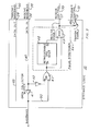
- Figure 1 depicts a baseband terminal A for connecting with a baseband data bus system and a terminal B for connection with a broadband data bus.
- Terminals A and B each comprise a pair of conductors, although only one is shown.
- Steering logic 10 is connected with the baseband terminal by means of data terminal 12 and with a transceiver 11 for providing the requisite transparency functions to the transceiver.
- Transceiver 11 which can be AM, FM or Phase Modulation, is connected to the broadband terminal by means of CARRIER terminal 27.
- the transceiver is connected to the steering logic by means of the DATA IN terminal 16 on the transceiver with the DATA OUT terminal 13 on the steering logic over transmit baseband line 15 and with the DATA OUT terminal 18 on the transceiver connected with the DATA IN terminal 14 on the steering logic over receive baseband line 17.
- the transmit/receive control (T/R) terminals 20, 9 of the transceiver 11 and steering logic 10 are interconnected by transmit/receive line 19.
- T/R signifies that when line 19 is high, the transceiver functions as a receiver of carrier signals and when line 19 is low, the transceiver functions as a transmitter of carrier signals.
- Baseband signals appearing at terminal A result in modulated carrier signals at broadband terminal B and modulated carrier signals appearing at the broadband terminal produce baseband signals at terminal A.
- the operation of the steering logic for the various types of modulation will be discussed in detail below.
- Figure 2 contains a transceiver 11 wherein the transmitter 22 and receiver 23 can be separately connected with the steering logic by means of a transmit baseband line 30 which connects the DATA IN terminal 29 on the transmitter with the DATA OUT terminal 28 on the steering logic and with a transmit-control line 33 which connects the transmit-control terminals 32, 31 on the transceiver and steering logic.
- a receive baseband line 36 interconnects the DATA OUT terminal 35 on the receiver with the DATA IN terminal 34 on the steering logic and a receive-control line 39 interconnects the receive-control terminal 38 on the receiver with the receive-control terminal 37 on the steering logic.
- the transmitter terminal 25 and the receiver terminal 26 interconnect with each other and with the broadband by means of a line 24. In the manner described earlier, baseband signals appearing at the baseband terminal produce modulated carrier signals at the broadband terminal and vice versa.
- the components within the steering logic 10 of Figures 1 and 2 for FSK, PSK or ASK modulation are shown in Figure 3 with the outputs of the steering logic arranged for connection with the separate receiver-transmitter embodiment of Figure 2, so that common reference numerals will be employed.
- the receive baseband line 36 is connected through terminal 34 with baseband terminal A through an open collector buffer 41, such as a Signe- tics Type 74LS07, over line 40 and through an inverter 42 with terminal 2 of an OR gate 43.
- a diode or a transistor can also be used as a buffer providing that the logic levels are suitable.
- Terminal 1 of OR gate 43 connects with the baseband terminal by means of line 50 and with the transmit baseband line 30 through line 65 and terminal 28.
- OR gate 43 The output of OR gate 43 is connected through a pulse stretcher 44 and terminal 37 to the receive-control line 39 and through an inverter 46 and terminal 31 to the transmit-control line 33.
- the T/R line 19 is connected with receive-control terminal 37, omitting inverter 46 and terminal 31.
- the pulse stretcher 44 comprises a retriggerable one-shot 48, such as a Motorola Type MC14528B monostable multivibrator, which is triggered on the rising edge of the output of the OR gate applied to terminal A of the one shot.
- the inverse output Q is connected to terminal 2 of an AND gate 49 and terminal 1 of the AND gate is connected to the output of the OR gate.
- the digital signals represented by the two states appearing at the baseband namely, the "supreme” state being a low voltage and impedance, will -also be referred to as “low”, and the "inferior” state being a high voltage and impedance, will also be referred to as "high”.
- the inactive state of the baseband bus is also high and in the inactive state the transmitter must transmit no carrier.
- the inactive state of the broadband bus is the absence of carrier.
- the two states of the baseband bus must be translated to two states of carrier on the broadband bus, such as frequency 1, frequency 2 (f l , f 2 ), or phase 1, phase 2 (0 ⁇ 1 , 0 ⁇ 2 ) or amplitude 1 , amplitude 2 (A1 , A2) where both Al and A2 are greater than zero.
- frequency 1, frequency 2 (f l , f 2 ) or phase 1, phase 2 (0 ⁇ 1 , 0 ⁇ 2 ) or amplitude 1 , amplitude 2 (A1 , A2) where both Al and A2 are greater than zero.
- the high state occurring within a message requires the transmission of carrier, but in the inactive state, must not result in carrier. If the baseband bus at terminal A is pulled low, the transmitter 22 is enabled and the receiver 23 is disabled.
- the purpose of the pulse stretcher 44 is to hold the transmitter 22 in the transmit mode for a duration longer than the maximum duration of any high state contained within a message in order to transmit the carrier state representative of the high state of the baseband bus. If the baseband is high longer than the time duration of the pulse stretcher, there is an inactive state and the transmitter 22 is disabled and the receiver 23 is enabled. When the receive baseband line 36 is pulled low by the presence of carrier having the proper state from another transceiver, the open collector buffer 41 pulls the baseband bus low and under this condition maintains the receiver 23 enabled and the transmitter 22 disabled. Since the baseband bus is maintained in the high. state by means of a bias resistor (not shown), all devices connected to the baseband bus drive the bus to the low state through a similar open collector buffer.
- the operation of the steering logic depicted in Figure 3 for ASK, FSK and PSK modulation can be seen by referring to the timing diagrams shown in Figure 4 for both transmitting and receiving modes.
- the inferior state is depicted as the high voltage and the superior state is depicted as the low voltage condition on the baseband waveform 51, transmit baseband waveform 52 and receive baseband waveform 53.
- the enable and disable state of the receive-control waveform 55 and transmit-control waveform 56, as well as the high and low states of the Q waveform 54, are depicted as high and low voltage conditions, respectively.
- the digital control device can then pull the baseband to the superior state.
- the baseband state controls the condition of the broadband in the transmitting mode and the broadband condition controls the state of the baseband in the receiving mode. Since the baseband terminal A and the transmit baseband line 30 are connected together by line 65, their waveforms 51, 52 are identical for both the transmit and receive modes. For purposes of this discussion, only the baseband waveform 51 will be referred to.
- the digital control device starts the transmitting mode, the baseband waveform 51 is in the superior state (low), transmit baseband line 30 is low and receive baseband line 36 is high.
- Both inputs 1, 2 to the OR gate 43 in Figure 3 are low resulting in a low state out of the OR gate which is applied to the one-shot 48 and to input 1 of the AND gate 49.
- the output to receive-control line 39 is low resulting in the disable state of the receive-control waveform 55.
- the AND gate output is inverted through inverter 46 to a high on transmit-control line 33 resulting in the enable state of the transmit-control waveform 56 as indicated.
- amplitude A 1 , frequency F 1 , or phase 0 1 will appear on the broadband as indicated at 63 in Figure 4.
- amplitude A 2 , frequency F 2 or phase 0 2 appear on the broadband as indicated at 64.
- the inactive state of the broadband comprises the absence of signal which is indicated at 62.
- the transmit-control waveform 56 In order to maintain the broadband signal in the second condition, A 2 , F 2 or ⁇ 2 during the time when the baseband is in the inferior state, the transmit-control waveform 56 must remain in the enable state. This is accomplished by triggering the pulse stretcher 44. Since input 2 to the OR gate 43 is always low when the receive baseband line 36 is high, the output of the OR gate will track the baseband. When the baseband goes to the inferior state, the OR gate output to the retriggerable one-shot input terminal A causes the one-shot output Q to remain low for a pre-determined time period greater than the longest anticipated inferior state in the message.
- This low state at the Q terminal is applied to terminal 2 of the AND gate 49 to maintain the receive-control line 39 and waveform 55 in the disable state and the transmit-control line 33 and waveform 56 in the enable state during the inferior state of the baseband.
- the retriggerable one-shot 48 is reset and starts retiming.
- the Q waveform 54 returns to the high state enabling the receiver, as indicated at 60 on the receive-control waveform 55 and disabling the transmitter as indicated at 61 on the transmit enable waveform 56 to complete the message.
- all other digital control devices connected to the broadband or baseband buses can now initiate a transmission according to a predefined bus access protocol.
- the carrier is either present or absent such that the supreme state corresponds to the presence of carrier as indicated at 66 in Figure 6 and the inferior state corresponds to the absence of carrier as indicated at 67.
- the simplified steering logic 10 of Figure 5 is employed.
- the pulse stretcher is not required since the broadband inferior state corresponding to the baseband inferior state is the absence of carrier which is the same as with the transmitter disabled.
- the receive baseband line 36 in Figure 5 connects through terminal 34, line 40 and inverter 42 with input 2 of the OR gate 43 and with the baseband terminal A through the open collector buffer 41.
- the baseband terminal A directly connects with the output side of the open collector buffer 41, input 1 of the OR gate over line 50 and with transmit baseband line 30 through terminal 28.
- the output of the OR gate connects with the receive-control line 39 through terminal 37 and with the transmit-control 33 through inverter 46 and terminal 31.
- the T/R line 19 is connected with receive control terminal 37, omitting inverter 46 and terminal 31.
- Transmit baseband line 30 is generally omitted with ASK 100% modulation since on-off keying does not usually require modulation input to the transmitter. If the baseband bus is pulled low by a digital control device, the transmitter is enabled and the receiver is disabled directly. When carrier is received on the broadband, the receive baseband line 36 pulls the baseband low, the receiver remains enabled and the transmitter remains disabled. Thus, the direct data exchange between broadband and baseband buses provides full transparency.
- the timing diagrams depicted in Figure 6 illustrate the conditions occurring at the baseband terminal A, the transmit baseband line 30, the receive baseband line 36, the receive-control line 39 and the transmit-control line 33 for the ASK 100% modulation employed with the steering logic 10 of Figure 5.
- the transmit-control and transmit baseband waveforms are identical so that only the transmit-control waveform 56 is depicted in Figure 6. Since the presence of carrier on the broadband corresponds to the superior state of the baseband and the absence of carrier corresponds to the inferior state of the baseband, the ASK modulation is depicted as A 1 and 0 (zero), respectively.
- the state recognition time is required in the receive mode to distinguish a true signal from noise, as described earlier.
- the transmit baseband line 30 in Figure 5 is pulled low and the receive baseband line 36 is high for the following reasons.
- Input 1 to OR gate 43 is low by direct connection with the baseband terminal over line 50 and input 2 is low by connection through inverter 42 with the high receiver baseband line 36 over line 40 resulting in a low at the OR gate output.
- the receive control line 39 is low by direct connection with the OR gate output and both the transmit control line 33 and transmit baseband line 30 are high by connection to the OR gate output through inverter 46.
- the baseband waveform 51 is in the superior state and the receive b aseband waveform 53 is in the inferior state as shown in Figure 6.
- the receive-control waveform 55 is in the disabled state while the transmit-control waveform 56 is in the enabled state.
- the digital control device allows the baseband bus to go high (inferior state) in the transmitting mode or in the inactive state, the receiving mode is invoked since the inferior state on the broadband bus is the absence of carrier.
- the receive baseband line 36 is low, which pulls the baseband bus low.
- Input 2 to OR gate 43 is high by connection with line 36 by means of terminal 24, line 40 and inverter 42. This is reflected in the superior state of the baseband waveform 51 and the low state of the receive baseband waveform 53 in Figure 6.
- the output of the OR gate is high which impresses a high on receive-control line 39 by connection through terminal 37.
- the transmit-control line 33 and transmit baseband line 30 are both low by connection with the OR gate output through inverter 46.
- the receive-control waveform 55 is in the enabled state and the transmit-control waveform 56 is in the disabled state as shown in Figure 6. It is seen, therefore, that ASK 100% modulation allows for the completely transparent exchange of data between the baseband bus and the broadband bus without the appearance of conflict. It will be readily appreciated by those skilled in the art that utilizing the steering logic concept teachings of the invention with suitable modifications will allow the use of a transceiver for other purposes and that the steering logic function can be achieved by other logic devices and circuits.
Applications Claiming Priority (2)
| Application Number | Priority Date | Filing Date | Title |
|---|---|---|---|
| US56148383A | 1983-12-14 | 1983-12-14 | |
| US561483 | 1995-11-20 |
Publications (3)
| Publication Number | Publication Date |
|---|---|
| EP0146045A2 true EP0146045A2 (de) | 1985-06-26 |
| EP0146045A3 EP0146045A3 (en) | 1986-08-06 |
| EP0146045B1 EP0146045B1 (de) | 1990-06-13 |
Family
ID=24242171
Family Applications (1)
| Application Number | Title | Priority Date | Filing Date |
|---|---|---|---|
| EP19840114505 Expired EP0146045B1 (de) | 1983-12-14 | 1984-11-29 | Digitaldatensender und -empfänger für ein Stromnetzübertragungssystem |
Country Status (4)
| Country | Link |
|---|---|
| EP (1) | EP0146045B1 (de) |
| JP (1) | JPS60169257A (de) |
| DE (1) | DE3482539D1 (de) |
| SG (1) | SG28293G (de) |
Cited By (4)
| Publication number | Priority date | Publication date | Assignee | Title |
|---|---|---|---|---|
| DE3503885A1 (de) * | 1984-02-08 | 1985-08-08 | General Electric Co., Schenectady, N.Y. | Sender/empfaenger |
| GB2188819A (en) * | 1986-03-19 | 1987-10-07 | Mitsubishi Electric Corp | Improved gateway for use in load control and text transmission systems |
| US6425030B1 (en) * | 1997-11-19 | 2002-07-23 | Menico Ag | Serial data-and control-bus with distribution voltage |
| US6694439B2 (en) * | 2000-06-07 | 2004-02-17 | Adaptive Instruments Corporation | Apparatus for providing communications data over a power bus having a total current that is the absolute value of the most negative current excursion during communication |
Citations (2)
| Publication number | Priority date | Publication date | Assignee | Title |
|---|---|---|---|---|
| US4099024A (en) * | 1977-02-16 | 1978-07-04 | Xerox Corporation | Communications network repeater |
| EP0038509A1 (de) * | 1980-04-18 | 1981-10-28 | Hewlett-Packard Limited | Logikschaltung zum Vermeiden eines Verriegelungszustandes zwischen voneinander entfernten Datenbussen |
Family Cites Families (3)
| Publication number | Priority date | Publication date | Assignee | Title |
|---|---|---|---|---|
| JPS5331568B2 (de) * | 1973-06-20 | 1978-09-04 | ||
| JPS5952587B2 (ja) * | 1979-11-05 | 1984-12-20 | 日本電信電話株式会社 | デ−タ伝送方式 |
| JPS5829241A (ja) * | 1981-08-14 | 1983-02-21 | Matsushita Electric Works Ltd | デ−タ通信方式 |
-
1984
- 1984-11-29 EP EP19840114505 patent/EP0146045B1/de not_active Expired
- 1984-11-29 DE DE8484114505T patent/DE3482539D1/de not_active Expired - Lifetime
- 1984-12-12 JP JP59260965A patent/JPS60169257A/ja active Granted
-
1993
- 1993-03-18 SG SG28293A patent/SG28293G/en unknown
Patent Citations (2)
| Publication number | Priority date | Publication date | Assignee | Title |
|---|---|---|---|---|
| US4099024A (en) * | 1977-02-16 | 1978-07-04 | Xerox Corporation | Communications network repeater |
| EP0038509A1 (de) * | 1980-04-18 | 1981-10-28 | Hewlett-Packard Limited | Logikschaltung zum Vermeiden eines Verriegelungszustandes zwischen voneinander entfernten Datenbussen |
Non-Patent Citations (3)
| Title |
|---|
| IEEE TRANSACTIONS ON NULCEAR SCIENCE, vol. NS-30, no. 4, part 1, August 1983, pages 2155-2157, IEEE, New York, US; J. SKELLY et al.: "A broadband accelerator control network" * |
| NACHRICHTEN ELEKTRONIK, vol. 36, no. 8, August 1982, pages 340-346, Heidelberg, DE; R. BOTH: "Lokale Netzwerke - Theorie und Praxis - Teil 2" * |
| WIRELESS WORLD, vol. 85, no. 1528, December 1979, pages 46-51, Haywards Heath, GB; N. McARTHUR et al.: "The intelligent plug" * |
Cited By (6)
| Publication number | Priority date | Publication date | Assignee | Title |
|---|---|---|---|---|
| DE3503885A1 (de) * | 1984-02-08 | 1985-08-08 | General Electric Co., Schenectady, N.Y. | Sender/empfaenger |
| GB2188819A (en) * | 1986-03-19 | 1987-10-07 | Mitsubishi Electric Corp | Improved gateway for use in load control and text transmission systems |
| US4763104A (en) * | 1986-03-19 | 1988-08-09 | Mitsubishi Denki Kabushiki Kaisha | Gateway for use in load control system |
| GB2188819B (en) * | 1986-03-19 | 1990-09-19 | Mitsubishi Electric Corp | Improved gateway for use in load control system |
| US6425030B1 (en) * | 1997-11-19 | 2002-07-23 | Menico Ag | Serial data-and control-bus with distribution voltage |
| US6694439B2 (en) * | 2000-06-07 | 2004-02-17 | Adaptive Instruments Corporation | Apparatus for providing communications data over a power bus having a total current that is the absolute value of the most negative current excursion during communication |
Also Published As
| Publication number | Publication date |
|---|---|
| SG28293G (en) | 1993-06-11 |
| EP0146045B1 (de) | 1990-06-13 |
| JPS60169257A (ja) | 1985-09-02 |
| DE3482539D1 (de) | 1990-07-19 |
| JPH0570348B2 (de) | 1993-10-04 |
| EP0146045A3 (en) | 1986-08-06 |
Similar Documents
| Publication | Publication Date | Title |
|---|---|---|
| US4723239A (en) | Serial bus system and method for selection of bus subscribers | |
| US4850042A (en) | Dual media local area network interfacing | |
| US4639933A (en) | Steering logic circuit for a digital data transceiver | |
| CA2151373A1 (en) | Method and apparatus for transmitting nrz data signals across an isolation barrier disposed in an interface between adjacent devices on a bus | |
| JPS5899046A (ja) | 星形通信網 | |
| AU1726988A (en) | Apparatus and method for providing a wireless link between two local area network systems | |
| US5150365A (en) | Communication system for coexistent base band and broad band signals | |
| KR940000981A (ko) | 컴퓨터 시스템, 시스템 확장장치, 버스 결합장치 및 버스억세스 조정방법 | |
| US5018139A (en) | Communication network between user equipment | |
| EP0113230B1 (de) | Datenübertragungssystem für ein lokales Netzwerk | |
| EP0146045B1 (de) | Digitaldatensender und -empfänger für ein Stromnetzübertragungssystem | |
| JP3529263B2 (ja) | 空間伝送用光送受信回路および空間伝送装置 | |
| US5155727A (en) | Method of coupling a data transmitter unit to a signal line and apparatus for performing the invention | |
| US4617423A (en) | Data communication system | |
| JPS58119247A (ja) | デ−タ通信方式 | |
| US4730250A (en) | Local area network processing system | |
| CA1232328A (en) | Digital data transceiver for power line communications system | |
| US5742608A (en) | Device for interfacing between communications media in a home systems network | |
| JPH07264160A (ja) | 通信ネットワーク及び通信局 | |
| CA2173949A1 (en) | A signal receiving and a signal transmitting unit | |
| US4711976A (en) | Data transmission facility | |
| US6731687B1 (en) | Dynamic line balancing scheme for providing inter-packet squelch | |
| GB2074426A (en) | Logic circuitry for intercommunication between distant bus systems | |
| JPH043702B2 (de) | ||
| JPH0659064B2 (ja) | 通信制御装置 |
Legal Events
| Date | Code | Title | Description |
|---|---|---|---|
| PUAI | Public reference made under article 153(3) epc to a published international application that has entered the european phase |
Free format text: ORIGINAL CODE: 0009012 |
|
| AK | Designated contracting states |
Designated state(s): DE FR GB NL |
|
| PUAL | Search report despatched |
Free format text: ORIGINAL CODE: 0009013 |
|
| AK | Designated contracting states |
Kind code of ref document: A3 Designated state(s): DE FR GB NL |
|
| 17P | Request for examination filed |
Effective date: 19870124 |
|
| 17Q | First examination report despatched |
Effective date: 19880805 |
|
| GRAA | (expected) grant |
Free format text: ORIGINAL CODE: 0009210 |
|
| AK | Designated contracting states |
Kind code of ref document: B1 Designated state(s): DE FR GB NL |
|
| REF | Corresponds to: |
Ref document number: 3482539 Country of ref document: DE Date of ref document: 19900719 |
|
| ET | Fr: translation filed | ||
| PLBE | No opposition filed within time limit |
Free format text: ORIGINAL CODE: 0009261 |
|
| STAA | Information on the status of an ep patent application or granted ep patent |
Free format text: STATUS: NO OPPOSITION FILED WITHIN TIME LIMIT |
|
| 26N | No opposition filed | ||
| REG | Reference to a national code |
Ref country code: GB Ref legal event code: IF02 |
|
| REG | Reference to a national code |
Ref country code: FR Ref legal event code: TP |
|
| REG | Reference to a national code |
Ref country code: FR Ref legal event code: D6 |
|
| PGFP | Annual fee paid to national office [announced via postgrant information from national office to epo] |
Ref country code: DE Payment date: 20031002 Year of fee payment: 20 |
|
| PGFP | Annual fee paid to national office [announced via postgrant information from national office to epo] |
Ref country code: GB Payment date: 20031006 Year of fee payment: 20 |
|
| PGFP | Annual fee paid to national office [announced via postgrant information from national office to epo] |
Ref country code: FR Payment date: 20031117 Year of fee payment: 20 |
|
| PGFP | Annual fee paid to national office [announced via postgrant information from national office to epo] |
Ref country code: NL Payment date: 20031118 Year of fee payment: 20 |
|
| PG25 | Lapsed in a contracting state [announced via postgrant information from national office to epo] |
Ref country code: GB Free format text: LAPSE BECAUSE OF EXPIRATION OF PROTECTION Effective date: 20041128 |
|
| PG25 | Lapsed in a contracting state [announced via postgrant information from national office to epo] |
Ref country code: NL Free format text: LAPSE BECAUSE OF EXPIRATION OF PROTECTION Effective date: 20041129 |
|
| REG | Reference to a national code |
Ref country code: GB Ref legal event code: PE20 |
|
| NLV7 | Nl: ceased due to reaching the maximum lifetime of a patent |
Effective date: 20041129 |