EP0141232A2 - Vector processing unit - Google Patents
Vector processing unit Download PDFInfo
- Publication number
- EP0141232A2 EP0141232A2 EP84111282A EP84111282A EP0141232A2 EP 0141232 A2 EP0141232 A2 EP 0141232A2 EP 84111282 A EP84111282 A EP 84111282A EP 84111282 A EP84111282 A EP 84111282A EP 0141232 A2 EP0141232 A2 EP 0141232A2
- Authority
- EP
- European Patent Office
- Prior art keywords
- vector
- data
- register
- arithmetic
- exception
- Prior art date
- Legal status (The legal status is an assumption and is not a legal conclusion. Google has not performed a legal analysis and makes no representation as to the accuracy of the status listed.)
- Granted
Links
Images


Classifications
-
- G—PHYSICS
- G06—COMPUTING; CALCULATING OR COUNTING
- G06F—ELECTRIC DIGITAL DATA PROCESSING
- G06F15/00—Digital computers in general; Data processing equipment in general
- G06F15/76—Architectures of general purpose stored program computers
- G06F15/80—Architectures of general purpose stored program computers comprising an array of processing units with common control, e.g. single instruction multiple data processors
- G06F15/8053—Vector processors
- G06F15/8076—Details on data register access
- G06F15/8084—Special arrangements thereof, e.g. mask or switch
-
- G—PHYSICS
- G06—COMPUTING; CALCULATING OR COUNTING
- G06F—ELECTRIC DIGITAL DATA PROCESSING
- G06F11/00—Error detection; Error correction; Monitoring
Definitions
- This invention relates to data processing apparatus, and more particularly to such apparatus that includes a functional unit using existing controls and data paths for scalar arithmetic to perform vector arithmetic in the functional unit designed for that purpose.
- U.S. Patent 4,128,880 describes a specially designed processor for vector processing that requires its own programming, and must rely on a host computer for providing it with vector data for processing. This patent also identifies other processors that provide very high speed processing for very large problems which provide capabilities well beyond the needs of many users.
- a main object of the invention is to provide a general purpose data processing system with high speed vector processing capability by simple connection of a vector processing functional unit to the base instruction handling and execution apparatus of the central processing unit (CPU).
- CPU central processing unit
- Another object of the invention is to provide vector processing for a base data processor having microprogramming control that only requires the microprogram control to provide an advance signal to the vector functional unit.
- a further object of the invention is to provide precise interrupt and error information to the base system suitable for accurate handling of vector exceptions.
- Another object of the invention is to provide a vector processing functional unit including addressable vector registers and masking capability to allow flexible handling of only certain elements of a longer string of elements.
- a hard-wired vector processing functional unit that includes addressable vector registers, a pipelined arithmetic unit that includes a parallel adder and multiply/divide unit, exception or error indicating logic that parallels the pipelined arithmetic unit, and masking logic for operand accessing control.
- the vector functional unit relies entirely on the instruction handling and control logic of a base processor, as well as the operand fetching and storing capabilities of the base unit for receiving instructions to execute, and vector elements to be operated on.
- the vector processing functional unit advances through vector processing in synchronism with the base machine by receiving an advance signal from the microprogram control of the base system.
- the vector processing functional unit arithmetic pipeline includes a plurality of stages, each of which includes exception or error indicating logic.
- the exception or error indicating logic inhibits the putaway of erroneous results, and provides error or exception information to the base system for the accurate handling and recovery from exception conditons.
- a mask register and logic provides flexibility in handling only certain elements of a long vector by consolidating certain elements in the vector storage of the vector functional unit. This requires less processing once the elements have been accessed, and makes the pipeline of the arithmetic unit more effective.
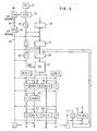
- FIG. 1 is a block diagram of a data processing system including a vector processing unit (VPU) 20 which is the subject of the present invention. With the exception of the VPU 20, the remainder of FIG. 1 represents a base data processing system more fully described in U.S. Patent 4,200,927 entitled Multi-Instruction Stream Branch Processing Mechanism. Further descriptions of the VPU 20 will refer to certain portions of the base data processing system including memory means 21 and a central processing unit (CPU) 22.
- VPU vector processing unit
- the memory means 21 includes processor storage 23 and processor storage control function (PSCF) 24.
- the memory means is utilized for the storage of program instructions and data operands including vectors to be processed by the VPU 20.
- the CPU 22 includes an instruction pre-processing function (IPPF) 25 and an E-function unit 26. These units are described in more detail in the above referred to U.S. Patent 4,200,927.
- IPPF 25 is responsible for fetching and decoding all instructions including those to be executed by the E-function 26 and those to be executed by the VPU 20.
- the E-function unit 26 executes non-vector processing instructions, provides a data path 27 between the E-function 26 and memory means 21, and includes a microprogam control store for generating instruction execution control signals.
- Interconnection of the VPU 20 with the base data processing system is by means of an interface 28 between the VPU 20 and E-function 26, and an interface 29 between the VPU 20 and the IPPF 25.
- FIG. 2 shows various functional units in the VPU 20 and CPU 22, and further detail involving the information that is transferred on interface 28 and interface 29 shown in FIG. 1.
- Interface 29 transfers vector instruction operation codes from the I element instruction queue 30 in the IPPF 25 to a vector instruction register 31 and Q instruction buffer 32 of the VPU 20.
- the interface 29 is also utilized to transfer address information between a vector index register 33 and a stride register 34.
- the stride register 34 contains address information specifying the main memory address separation between elements of a vector of ordered elements.
- FIG. 2 Further details of the interface 28 between the VPU 20 and E-function 26 of the CPU 22 are shown in FIG. 2.
- the transfer of data between the VPU 20 and the memory means 21 of FIG. 1 includes a data bus 35.
- Data from the memory system 21 of FIG. 1 to the VPU 20 includes the data bus 27, register 36 of the E-function 26, data bus 35, to a data in register 37 in the VPU 20.
- Data to be transferred from the VPU 20 to the memory system 21 of FIG. 1 includes data from register 38 or lambda register 39 in the VPU 20 over the bus 35, which is bidirectional, to a register 40 in the E-function 26 to the bus 27.
- One error condition that can occur is the detection of an error in data accessed from the memory system 21 to the E-function 26. Rather than reacting to the detection of an error in the E-function 26, which would normally cause all processing to cease, the access exception will be noted at 41 in the E-function 26, and be passed over a line 42 to an access exception mechanism 43 in the VPU 20. The access exception noted at 43 will be utilized at a subsequent time to provide more accurate information as to how far instruction processing has progressed on a long string of vector elements. This will be described subsequently.
- error conditions that can occur involve the detection of arithmetic errors in the VPU 20.
- an exception code is provided at 44 and passed over a line 45 to status indicators 46 in the CPU 22.
- the arithmetic exceptions are indicated by a coded representation and stored in the status triggers 46 for analysis by the CPU 22 to determine corrective action to take.
- the E-function 26 has as its basic control mechanism a microprogram control store 47.
- a branch, or change in sequence of microinstruction execution in the control store 47, is signalled by logic 48 indicating various branch points.
- Several signal lines, representing branch requirements, are signalled by service requests 49 from the VPU 20 which are transferred on a line 50 to the branch point logic 48.
- FIG. 2 One final line shown in FIG. 2, which is a part of the interface 28 of FIG. 1, is line 51.
- a decoder provides execution control signals to the E-function 26 of the CPU 22.
- timing control of the operation in the VPU 20 is effected by the basic clock cycles of the CPU 22.
- the sequencing of various functions in the VPU 20 is under control of a signal on line 51 from the decoding of data register 52. This signal is labelled advance 53. All timing and gate energization in the VPU 20 is synchronized with, and under control of, microinstruction sequencing indicated on line 51, and responds to an advance pulse on line 54 which goes to all of the logic and gates of the VPU 20.
- FIG. 3 shows certain of the VPU 20 status information signalled on line 50 of FIG. 2, which status information is utilized in the branch points logic 48 to control sequencing of microinstructions from control store 47.
- signal lines 55 and 56 show vector processing related signal lines from the IPPF 25 and E-function 26 in FIG. 2. Branching in the microinstruction sequencing of control store 47 will occur from certain VPU 20 conditions indicating readiness of the VPU 20, the requirement for an operand fetch or store, end of a vector instruction, and a vector exception indication.
- FIG. 4 shows various paths, registers, and functional units of the VPU 20 of the present invention. Certain of the registers and buses dealing with the interface between the VPU 20 and the CPU 22 have already been referred to in connection with FIG. 2.
- the buses include the interface lines 29 and 35.
- Registers include data in register 37, register 38 and 39 labelled stage A and lambda respectively, the instruction register 31, instruction buffer 32, and the address index register 33.
- FIG. 4 there is shown a vector register array 57.
- the array 57 contains 16 vector registers (VR's), with each VR consisting of 128 four-byte elements.
- the VR's can be coupled (even-odd paired) to form double word operands.
- Addressing of the vector register array 57 involves a number of address registers which will be subsequently described, but which are noted generally in FIG. 4 at 58.
- Stage A register 38 and stage B register 59 accept data that is read from the VR's 57. From register 38, the data goes either to the vector data path or the E-function 26, depending on the instruction. Register 38 can also accept data from a vector mask register (VMR) on a line 60. The function of the VMR will be described subsequently.
- Register 39 is used as a delay register for the arithmetic data flow as well as a back-up register for data being sent to the E-function 26 from register 38. The data delay is necessary to implement proper VR access.
- Registers 61 and 62 receive information from a variety of sources. Their outputs are to pre-shifting logic used during exponent alignment for floating point operations.
- the ALU in registers 63 and 64 respectively are staging registers that contain data to be processed by the ALU 65.
- the arithmetic and logic unit (ALU) 65 is a parallel binary adder.
- the ALU out register 66 holds the output of the ALU 65 from the previous cycle.
- Post i normalizing logic 67 is provided for floating point operations.
- the ALU put away register 68 receives its input from the post normalizing logic 67.
- Register 68 serves as a delay register for data that is to recycle to the ALU 65.
- Index register 33 has an input from register 68.
- the index register 33 is used to hold the addresses generated during index type instructions. When appropriate, the address is then sent to the address incrementor in the IPPF 25 shown in FIG. 2.
- the VR put away register 69 serves as a stage for data that is to be written into the VR array 57. Its inputs are from register 37 or from a put away bus 70 which has several sources.
- Registers 71 and 72 are a multiply stage A register and a multiply stage B register respectively. These registers contain data that is fed to the remainder of the multiply data path including exponent summation logic 73.
- the multiplicand A stage register 74 holds the multiplicand for a multiply operation and the divisor for a divide operation. It also buffers the dividend during divide functions.
- the multiplier register 75 stores the multiplier for multiply operations and recoded quotients of divide operations.
- the output of registers 74 and 75 provide inputs to a multiply/divide unit 76.
- the remainder of the multiply/divide data path includes, at the output of the multiply/divide unit 76, a product/quotient register 77, and post normalizing logic 78.
- the final register in the multiply/divide data path is the multiply put away register 79 which is fed from the post normalizing logic 78, and serves as a delay register for data that is to be fed to the data path of the ALU 65 for certain compound vector instructions and for all vector divide instructions as part of the divide function.
- the data in register 37 serves as a buffer for data coming from register 36 in the E-function 26 of FIG. 2.
- the ALU 65 is an arithmetic and logic unit which performs addition and subtraction on binary, short precision, and long precision operands.
- the ALU 65 can also perform the AND, OR, and EXOR logical operations, and logically shift an operand 0, 1, 2, or 3 bits left.
- the instruction buffer 32 which receives information on the interface 29, retains the vector instruction op code and vector register addresses for use by other decode circuits in the VPU 20 during instruction execution.
- vector operand data comes from either the VR array 57 or the CPU 22 through the data in register 37.
- the first vector element fetched goes through the A-side of the data path.
- the second vector elements go through the B-side of the data path. All parts of the appropriate data path (ALU 65 or multiply-divide unit 76) are stepped simultaneously. Initially, the first element of the A-side vector operand is read out of the VR's 57 one cycle earlier than the first element of the B-side vector operand.
- A-side element 1 is in the lambda register 39
- the B-side element 1 is in the stage B register 59
- A-side element 2 is in the stage A register 38.
- This initial offset is to accommodate the single port array chips that comprise the VR's 57.
- This offset in conjunction with the arrangement of logical vectors in the physical array chips, to be subsequently described, guarantees that only one read is made from any array chip during any given cycle.
- a vector result from the VR put away register 69 can be stored into the VR's 57 each machine cycle.
- the vector from the VR 57 flows through the B-side of the data path.
- the vector from storage comes from the E-function 26, into the data in register 37, and then through the A-side of the data path beginning at either the ALU shift A register 61 or the multiply stage A register 71.
- the vector result is written into a destination VR 57, as specified by the instruction.
- the CPU 22 uses a signal to put the scalar operand into the A-side of either the ALU 65 or the multiply-divide unit 76 data path.
- the scalar operand is held in either the ALU shift A register 61 or the multiply stage A register 71 and is fed to the subsequent logic.
- the VR 57 operand flows through the B-side of the data path. The result is then written into a destination VR 57.
- the CPU 22 When there is one vector from the memory system 21 and one scalar element from the E-function 26, the CPU 22 generates a signal to put the scalar operand into the A-side of either the ALU 65 or the multiply/divide unit 76 data path. The CPU 22 then issues an advance signal to step the vector storage operand through the B-side of the data path. The result will then be written into a destination VR 57.
- the data transfer path for a vector load instruction is from the CPU 22 register 36, onto the data bus 35, and into the data in register 37.
- the data is then stored into a VR 57 through the VR put away register 69.
- a vector element address register to be discussed, is incremented by 1.
- the CPU 22 calculates storage addresses of vector elements, makes a fetch request to storage, and transfers data at a maximum rate of one element per cycle.
- the bit mask is examined and determines whether or not a particular element is to be 20 loaded into a VR 57.
- the VPU 20 calculates the storage addresses. The address is then sent to the CPU 22 on interface 29 which makes the fetch request and transfers the data to the VPU 20 on the data bus 35.
- the VPU 20 transfers data to the CPU 22 from a VR 57, through the stage A register 38, and onto the bidirectional data bus 35. If a clock stopping situation should occur in the CPU 22, a signal becomes active in the VPU 20 one cycle later. The data that was to be placed onto the data bus 35 is held in the lambda register 39. When execution resumes, the data in the lambda register 39 is put onto the data bus 35. As with vector load instructions, address calculations, vector mask utilization, and index vector usage is accomplished in the same manner.
- FIG. 5 Positive control of the cycling of the VPU 20 by the CPU 22 is shown in FIG. 5.
- Elements previously referred to in the CPU 22 include the control store 47, the control store data register 52, and register 36.
- the positive control exercised by the CPU.22 is effected by detecting a particular micro-order of a particular microinstruction in the control store data register 52 which sets a one cycle trigger 80 labelled CP advance.
- Signal line 51 will be energized and effective at 53 to generate a VP advance signal 54 which is applied to all data path gates between stages of the VPU 20 data path.
- the vector data does not advance through the data path unless the advance signal 54 is present. This assures synchronization and positive CPU 22 control over the VPU 20.
- each register in the data flow retains its data. Otherwise, the data is ingated as directed by instructions in the VPU 20.
- a data valid bit which parallels the functional data path in the VPU 20.
- the initial data valid bit shown at 81 is associated with the data register 36 in the CPU 22, and is set by a microinstruction micro-order to indicate that the contents of the register 36 are valid and can be gated to the VPU 20.
- the function of the data valid bits is to guarantee validity of the data being processed in a particular stage. Absence of the data valid bit associated with put away register 69 prevents updating of a VR 57.
- the CPU 22 or output of a VR 57 depending on the source of operands, raises the data valid bit with each element to be processed, and drops the data valid bit after the last element is processed.
- a counter is incremented to provide an indication of the number of vector elements that have been properly processed. This counter also indicates completion of processing of all elements in a vector. This counter is utilized in those situations where errors occur, and a need arises to indicate the total number of elements that have been properly processed when the processing is resumed for a particular vector instruction.
- the passage of data valid bits through the data path is configured by control lines dependent upon a particular vector instruction being executed. All of the other elements shown in FIG. 5 have been previously referred to and have been given the same numeric designations.
- FIG. 6 shows two configurations of the data flow path in the VPU 20 for two representative vector instructions.
- the solid lines of the data path indicate a configuration for doing a VR accumulate instruction, and the dotted path shows a configuration for performing a VR and main storage multiply and accumulate instruction.
- the first partial sum from the A side of the data flow enters the ALU put away register 68.
- the next advance transfers the ALU put away register 68 contents into the ALU shift A register 61 on line 83 while the stage B register 59 contents are transferred to the ALU shift B register 62.
- the VR put away register 69 places accumulated results into one of four partial sum locations of a VR 57.
- the ALU put away register 68 wraps the results back to the ALU shift A register 61. This partial sum is then fed into the ALU 65 with another element from the B side and the operation continues.
- the result of the accumulate instruction is that every fourth element is added and the results are put into one of four partial sum locations of a vector register.
- the dotted lines of FIG. 6 show a configuration for multiply and accumulate utilizing data from main storage.
- the first advance gates data from storage to the data in register 37 and the first element of a VR 57 operand into the stage B register 59.
- a second advance gates data in register 37 to multiply stage A register 71, stage B register 59 to the multiply stage B register 72, and the first partial sum into stage A register 38.
- the gates energized by the second advance are used for five more cycles. At this time, ⁇ ive more elements have been read into the data flow of the multiply/divide unit 76. However, data in the multiply put away register 79 has not yet been marked valid and the partial sum 0 is in ALU put away register 68.
- the data flow for the ALU 65 is blocked from further advances until the multiply put away register 79 indicates valid data.
- the next advance gates the ALU put away register 68 to the ALU shift A register 61 and the multiply put away register 79 to the ALU shift B register 62.
- the accumulated results of the first partial sum and the multiply result along with the valid bit reach the ALU put away register 68 and VR put away 69. Writing of results into the vector register 57 starts when the first sum of the product and partial sum 0 reaches ALU put away 68.
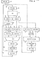
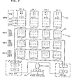
- FIGS. 7, 8, and 9 show the logical configuration of the vector register array 57 and the vector register array addressing mechanism shown generally at 58 in FIG. 4.
- the array 57 contains 16 vector registers (VR's), with each register consisting of 128 four-byte elements.
- the VR's can be coupled (even-odd paired) to form double word operands.
- the entire array is in 64 array chips 85.
- Each chip 85 is one byte of nine bits wide (eight bits plus parity). Because the array chip 85 is limited to a single read/write per cycle, it is necessary to four-way interleave the VR's as shown in FIG. 7.
- Each column of the array represents one interleave which consists of 16 chips 85 grouped by four.
- Each row of the array 57 represents four VR's.
- FIG. 7 shows the data path for reading out from the VR registers to a stage register such as 38, and FIG. 8 shows the reading of data into the VR's through the VR put away register 69.
- VEARs vector element address registers
- VEAR 1 contains the number of the element of the vector that is being written into the VR's.
- VEAR 1 is also utilized as a vector interruption index (VIX) for most vector instructions that write results into the VR's.
- VIP vector interruption index
- Each VEAR is updated by its own incrementor and is loaded from data in register 37 shown in FIG. 4.
- the VIX is incremented only when a data valid signal associated with the VR put away register 69 is effective to permit a writing into the VR's. Therefore, if an error condition indicates that a VR should not be updated, the VIX will not be stepped and will provide an indication of the number of elements that have been processed during a particular instruction execution. This information can be utilized when the instruction is re-initiated after any fix-up routines.
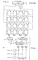
- the addressing mechanism also includes three vector address registers (VAR's) noted generally at 87 in FIG. 9.
- VAR's are labelled VAR 1, VAR 2, and VAR 3.
- VAR 2 and VAR 3 normally contain the numbers of the source VR's whose elements are being read.
- VAR 1 contains the number of the destination VR whose element is being written.
- Bits five and six of a VEAR 86 provide a column select (CS) on line 88, and bits two and three of a VAR 87 provide row select (RS) on a line 89.
- the seven-bit address shown at 90 is utilized for addressing a particular one of 128 locations in each of the array chips 85.
- each column can be addressed independently.
- the same address is presented to all 16 array chips 85 in a column so it is possible to write into one column and read out of any one of the other three.
- Data selection is done in the logic chip before gating into the stage registers.
- Short operands are presented to both halves of the stage register, for example register 38. For long operands, the even register element goes to the left half (0-31) and the odd register goes to the right half (32-63), as shown in FIG. 7.
- FIGS. 10, 11 and 12 show various uses of a mask register during vector 5 processing.
- the vector mask register (VMR) logically consists of 128 bits, any one of which can be set or reset by processing in the VPU 20. It can be loaded with information from the main store or its content stored in main store at a rate of eight bits per cycle.
- the 128 bits of the mask register correspond to the 128 elements of a vector stored in the VR's.
- the 128 bits of the mask register are implemented as a VMR array 91 further configured as 16 eight-bit registers. The use of a particular binary bit of the VMR is selected by a VMR address register 92 and bit select logic 93.
- Bits 0-3 of the VMR address register 92 select one of the sixteen registers in the VMR array 91, and bits 4-6 select a particular one of the eight binary bits of the selected register.
- a choice of whether or not to use masking during arithmetic and logic processing is made by the set or reset state of a vector mode trigger 94.
- An OR gate 95 is enabled to provide an output 96 either by the vector mode trigger 94 or when a particular mask bit selected from bit select 93 is a binary one.
- a first group of instructions involving the mask register are comprised of arithmetic and logic instructions.
- each element of a vector flows through the data flow, undergoes the operation, and the result is put away in the VR's 57. If however the mode trigger 94 is off, then the operation proceeds as before but with one exception.
- ALU 65 results are advanced to the ALU out register 66, and the valid bit 97 set, the signal 96 indicating a mask bit of binary one will be effective to gate the valid bit 97 to the valid bit 98 associated with the VR put away register 69.
- a vector mask register bit of binary 0 will not cause the ALU output result to be stored in the VR's 57.
- the vector mask register address register 92 is incremented by 1 for each result that is stored in the ALU out register 66.
- the mask bits are utilized in an instruction called load expanded.
- vector elements are transferred to the data in register 37 from the CPU 22 from sequential addresses in main memory along with a data valid bit.
- the vector element address register 86 associatd with the destination VR 57 is incremented by 1 along with the VMR address register 92. Only those elements of the destination VR 57 associated with a vector mask bit that is a binary 1, will receive data from put away register 69, setting the data valid at 98 to cause storage of the element in a VR 57.
- FIG. 13 and 14 The manner in which the VPU 20 provides accurate information regarding i exception or error conditions is shown in FIG. 13 and 14. Various stages of the VPU 20 data flow are shown in these figures and have been given the same numeric designation as previously discussed.
- the data path for storage access exceptions is shown in FIG. 13.
- a data path of exception bits dealing with storage access exceptions parallels the functional data path in the VPU 20. There is one exception bit per data path stage. This exception data path is used for instructions that use a vector from the main storage element 21 of FIG. 1. If an access exception is detected in the storage system for a particular element, the CPU 22 raises the signal on line 42 (which is normally 0) and passes it on to the VPU 20 along with the bad data.
- the signal is put into the access exception data path, beginning at the data in register 37 and starts in the parallel data path at 43.
- This active bit flows with the bad data, and inhibits the put away of that data into the VR's 57.
- the VPU 20 signals the access exception to the CPU on line 100, and inhibits all further put away of data for this instruction.
- the line 100 corresponds to the line labelled vector put away exception shown in FIG. 3, and is applied to the branch logic 48 associated with the control store 47 shown in FIG. 2.
- the access exception data path is configured by control lines in accordance with the instruction being executed.
- the CPU 22 microcode branches out of its processing loop into a common ending routine for all vector instructions that encounter an exception.
- the microcode uses the VIX which is represented by the count state of the VEAR 1 representing the destination vector register, to calculate the storage address of the element with the exception.
- the microcode issues a fetch to the failing location and enters the standard interrupt handling routine.
- logic noted generally at 101 passes the access exception to the CPU 22, and blocks the updating of the VR's 57 for data contained in the VR put away register 69.
- Three inputs to the logic 101 include a signal on line 102 indicating an access exception for an instruction that would normally load the VR's 57 from the data in register 37.
- Signal line 103 indicates an access exception noted for data in the ALU out register 66, and line 104 signals the access exception at the time prior to put away from the multiply/divide unit 76.
- a signal on line 105 deals with arithmetic exceptions discussed in FIG. 14.
- FIG. 14 shows a data path of arithmetic exception bits which parallels part of the data path of the VPU 20.
- the type of exception noted is encoded into a three-bit word.
- the three-bit code is sent from the VPU 22 to status triggers in the CPU 22 over the line 45, previously referred to in connection with FIG. 2. As shown at 106, the three-bit exception code will not be transferred to the CPU 22 when there is also an access exception indicated in FIG. 13.
- the arithmetic exception path also parallels the data path in the VPU 20.
- arithmetic exceptions may be discovered.
- a divide by 0 and unnormalized operand exception may be encountered.
- a multiply overflow and underflow exception may be encountered, as noted at 108, just prior to the multiply put away register 79.
- an ALU overflow, underflow, and significance loss exception may be encountered just prior to ALU put away register 68.
Landscapes
- Engineering & Computer Science (AREA)
- Theoretical Computer Science (AREA)
- Computer Hardware Design (AREA)
- Physics & Mathematics (AREA)
- General Engineering & Computer Science (AREA)
- General Physics & Mathematics (AREA)
- Computing Systems (AREA)
- Quality & Reliability (AREA)
- Complex Calculations (AREA)
- Advance Control (AREA)
Abstract
Description
- This invention relates to data processing apparatus, and more particularly to such apparatus that includes a functional unit using existing controls and data paths for scalar arithmetic to perform vector arithmetic in the functional unit designed for that purpose.
- The following U.S. patents are representative of existing data processing configurations that provide vector data processing.
- U.S. Patent 4,128,880 describes a specially designed processor for vector processing that requires its own programming, and must rely on a host computer for providing it with vector data for processing. This patent also identifies other processors that provide very high speed processing for very large problems which provide capabilities well beyond the needs of many users.
- The other extreme for processing vector operands is represented by U.S. Patent 4,172,287. A general purpose data processor originally designed for scalar arithmetic, including an arithmetic and logic unit designed for handling a pair of operands for each instruction executed, has been modified to recognize vector instructions. Most of the modifications deal with handling memory address arithmetic for vector element accessing. A vector buffer has been added for use in only a very specific memory addressing situation to provide some speed enhancement for overall processing. However, even with these modifications, the original arithmetic unit is still utilized. In this latter prior art patent, an additional store for vector instruction microprogramming is also required thereby retaining the speed degradation inherent in this form of execution control. Also, the interrupt handling capability of the basic processor must be relied upon, providing a lesser degree of accuracy of error handling in vector processing situations.
- A main object of the invention is to provide a general purpose data processing system with high speed vector processing capability by simple connection of a vector processing functional unit to the base instruction handling and execution apparatus of the central processing unit (CPU).
- Another object of the invention is to provide vector processing for a base data processor having microprogramming control that only requires the microprogram control to provide an advance signal to the vector functional unit.
- A further object of the invention is to provide precise interrupt and error information to the base system suitable for accurate handling of vector exceptions.
- Another object of the invention is to provide a vector processing functional unit including addressable vector registers and masking capability to allow flexible handling of only certain elements of a longer string of elements.
- These and other objects, features, and advantages of the invention as claimed, are realized in a hard-wired vector processing functional unit that includes addressable vector registers, a pipelined arithmetic unit that includes a parallel adder and multiply/divide unit, exception or error indicating logic that parallels the pipelined arithmetic unit, and masking logic for operand accessing control. The vector functional unit relies entirely on the instruction handling and control logic of a base processor, as well as the operand fetching and storing capabilities of the base unit for receiving instructions to execute, and vector elements to be operated on. The vector processing functional unit advances through vector processing in synchronism with the base machine by receiving an advance signal from the microprogram control of the base system.
- The vector processing functional unit arithmetic pipeline includes a plurality of stages, each of which includes exception or error indicating logic. The exception or error indicating logic inhibits the putaway of erroneous results, and provides error or exception information to the base system for the accurate handling and recovery from exception conditons.
- A mask register and logic provides flexibility in handling only certain elements of a long vector by consolidating certain elements in the vector storage of the vector functional unit. This requires less processing once the elements have been accessed, and makes the pipeline of the arithmetic unit more effective.
-
- FIG. 1 is an overall block diagram of an existing data processing system with the vector processing functional unit of the present invention included.
- FIG. 2 shows the major interface lines between the central processing unit (CPU) of a base data processor and the vector processor of the present invention.
- FIG. 3 shows the signals presented to the microprogram branching logic of a base data processor for dealing with vector processing.
- FIG. 4 shows the functional elements of the vector processing unit of the present invention and the controllable interconnection of these elements in a data flow path.
- FIG. 5 shows the data path of the vector processing unit of the present invention and the control of data advance by the microprogram control of a base system.
- FIG. 6 shows the interconnection of elements of the vector processor of the present invention for executing two representative vector instructions.
- FIG. 7 shows the arrangement of vector registers in the vector processing unit of the present invention and the output data path.
- FIG. 8 shows the arrangement of vector registers in the vector processing unit of the present invention and the input data path.
- FIG. 9 shows the addressing logic for the vector registers of the vector i processing unit of the present invention.
- FIG. 10 shows the use of masking associated with elements of a vector during arithmetic operations in the vector processing unit of the present invention.
- FIG. 11 shows the use of masking associated with elements of a vector during loading of elements from main memory into vector registers.
- FIG. 12 shows the use of masking associated with elements of a vector during storing of elements in main memory from vector registers.
- FIG. 13 shows the logic of the vector processing unit of the present invention responding to an access exception indicating an error encountered during the access of an element from main storage.
- FIG. 14 shows the logic of the vector processing unit of the present invention responding to an arithmetic exception indicating an error encountered during arithmetic processing in the vector processing unit of the present invention.
- FIG. 1 is a block diagram of a data processing system including a vector processing unit (VPU) 20 which is the subject of the present invention. With the exception of the
VPU 20, the remainder of FIG. 1 represents a base data processing system more fully described in U.S. Patent 4,200,927 entitled Multi-Instruction Stream Branch Processing Mechanism. Further descriptions of theVPU 20 will refer to certain portions of the base data processing system including memory means 21 and a central processing unit (CPU) 22. - The memory means 21 includes
processor storage 23 and processor storage control function (PSCF) 24. The memory means is utilized for the storage of program instructions and data operands including vectors to be processed by theVPU 20. TheCPU 22 includes an instruction pre-processing function (IPPF) 25 and anE-function unit 26. These units are described in more detail in the above referred to U.S. Patent 4,200,927. The IPPF 25 is responsible for fetching and decoding all instructions including those to be executed by theE-function 26 and those to be executed by theVPU 20. As more fully described in the above referred to patent, theE-function unit 26 executes non-vector processing instructions, provides adata path 27 between theE-function 26 and memory means 21, and includes a microprogam control store for generating instruction execution control signals. - Interconnection of the
VPU 20 with the base data processing system is by means of aninterface 28 between theVPU 20 andE-function 26, and aninterface 29 between theVPU 20 and the IPPF 25. - FIG. 2 shows various functional units in the
VPU 20 andCPU 22, and further detail involving the information that is transferred oninterface 28 andinterface 29 shown in FIG. 1. -
Interface 29 transfers vector instruction operation codes from the Ielement instruction queue 30 in theIPPF 25 to avector instruction register 31 andQ instruction buffer 32 of theVPU 20. - The
interface 29 is also utilized to transfer address information between avector index register 33 and astride register 34. Thestride register 34 contains address information specifying the main memory address separation between elements of a vector of ordered elements. - Further details of the
interface 28 between theVPU 20 andE-function 26 of theCPU 22 are shown in FIG. 2. The transfer of data between theVPU 20 and the memory means 21 of FIG. 1 includes adata bus 35. Data from thememory system 21 of FIG. 1 to theVPU 20 includes thedata bus 27, register 36 of theE-function 26,data bus 35, to a data inregister 37 in theVPU 20. Data to be transferred from theVPU 20 to thememory system 21 of FIG. 1 includes data fromregister 38 orlambda register 39 in theVPU 20 over thebus 35, which is bidirectional, to aregister 40 in theE-function 26 to thebus 27. - A great deal of arithmetic pipelining takes place in the
VPU 20, and a great deal of address arithmetic takes place when long vectors are processed. When various error conditions occur, either in theCPU 22 orVPU 20, it is important to indicate the precise point in the sequence of an instruction execution where an error condition occurred. - One error condition that can occur is the detection of an error in data accessed from the
memory system 21 to theE-function 26. Rather than reacting to the detection of an error in theE-function 26, which would normally cause all processing to cease, the access exception will be noted at 41 in theE-function 26, and be passed over aline 42 to anaccess exception mechanism 43 in theVPU 20. The access exception noted at 43 will be utilized at a subsequent time to provide more accurate information as to how far instruction processing has progressed on a long string of vector elements. This will be described subsequently. - Other error conditions that can occur involve the detection of arithmetic errors in the
VPU 20. In response to arithmetic errors, an exception code is provided at 44 and passed over aline 45 tostatus indicators 46 in theCPU 22. The arithmetic exceptions are indicated by a coded representation and stored in the status triggers 46 for analysis by theCPU 22 to determine corrective action to take. - As referred to earlier, and shown in FIG. 2, the
E-function 26 has as its basic control mechanism amicroprogram control store 47. A branch, or change in sequence of microinstruction execution in thecontrol store 47, is signalled bylogic 48 indicating various branch points. Several signal lines, representing branch requirements, are signalled byservice requests 49 from theVPU 20 which are transferred on aline 50 to thebranch point logic 48. - One final line shown in FIG. 2, which is a part of the
interface 28 of FIG. 1, isline 51. As microinstructions are read fromcontrol store 47, and placed in adata register 52, a decoder provides execution control signals to theE-function 26 of theCPU 22. As part of the present invention, timing control of the operation in theVPU 20 is effected by the basic clock cycles of theCPU 22. The sequencing of various functions in theVPU 20 is under control of a signal online 51 from the decoding of data register 52. This signal is labelledadvance 53. All timing and gate energization in theVPU 20 is synchronized with, and under control of, microinstruction sequencing indicated online 51, and responds to an advance pulse online 54 which goes to all of the logic and gates of theVPU 20. - FIG. 3 shows certain of the
VPU 20 status information signalled online 50 of FIG. 2, which status information is utilized in thebranch points logic 48 to control sequencing of microinstructions fromcontrol store 47. Also,signal lines IPPF 25 and E-function 26 in FIG. 2. Branching in the microinstruction sequencing ofcontrol store 47 will occur fromcertain VPU 20 conditions indicating readiness of theVPU 20, the requirement for an operand fetch or store, end of a vector instruction, and a vector exception indication. - FIG. 4 shows various paths, registers, and functional units of the
VPU 20 of the present invention. Certain of the registers and buses dealing with the interface between theVPU 20 and theCPU 22 have already been referred to in connection with FIG. 2. The buses include theinterface lines register 37, register 38 and 39 labelled stage A and lambda respectively, theinstruction register 31,instruction buffer 32, and theaddress index register 33. - The function of these registers, and others to be further described, and the arithmetic units will now be described. In FIG. 4, there is shown a
vector register array 57. Thearray 57 contains 16 vector registers (VR's), with each VR consisting of 128 four-byte elements. The VR's can be coupled (even-odd paired) to form double word operands. Addressing of thevector register array 57 involves a number of address registers which will be subsequently described, but which are noted generally in FIG. 4 at 58. - Stage A
register 38 andstage B register 59 accept data that is read from the VR's 57. Fromregister 38, the data goes either to the vector data path or the E-function 26, depending on the instruction.Register 38 can also accept data from a vector mask register (VMR) on aline 60. The function of the VMR will be described subsequently.Register 39 is used as a delay register for the arithmetic data flow as well as a back-up register for data being sent to the E-function 26 fromregister 38. The data delay is necessary to implement proper VR access. -
Registers registers ALU 65. The arithmetic and logic unit (ALU) 65 is a parallel binary adder. The ALU outregister 66 holds the output of theALU 65 from the previous cycle. Post i normalizinglogic 67 is provided for floating point operations. The ALU put awayregister 68 receives its input from thepost normalizing logic 67.Register 68 serves as a delay register for data that is to recycle to theALU 65.Register 68, together withregister 61, register 63, and register 66, form a four cycle closed path circuit that is used for vector accumulate instructions to be subsequently described. - Index register 33 has an input from
register 68. Theindex register 33 is used to hold the addresses generated during index type instructions. When appropriate, the address is then sent to the address incrementor in theIPPF 25 shown in FIG. 2. - The VR put away
register 69 serves as a stage for data that is to be written into theVR array 57. Its inputs are fromregister 37 or from a put awaybus 70 which has several sources. -
Registers exponent summation logic 73. The multiplicandA stage register 74 holds the multiplicand for a multiply operation and the divisor for a divide operation. It also buffers the dividend during divide functions. The multiplier register 75 stores the multiplier for multiply operations and recoded quotients of divide operations. - The output of
registers divide unit 76. The remainder of the multiply/divide data path includes, at the output of the multiply/divide unit 76, a product/quotient register 77, and post normalizinglogic 78. The final register in the multiply/divide data path is the multiply put awayregister 79 which is fed from thepost normalizing logic 78, and serves as a delay register for data that is to be fed to the data path of theALU 65 for certain compound vector instructions and for all vector divide instructions as part of the divide function. - The data in
register 37, previously referred to, serves as a buffer for data coming fromregister 36 in theE-function 26 of FIG. 2. TheALU 65 is an arithmetic and logic unit which performs addition and subtraction on binary, short precision, and long precision operands. TheALU 65 can also perform the AND, OR, and EXOR logical operations, and logically shift anoperand - The
instruction buffer 32 which receives information on theinterface 29, retains the vector instruction op code and vector register addresses for use by other decode circuits in theVPU 20 during instruction execution. - Still referring to FIG. 4, vector operand data comes from either the
VR array 57 or theCPU 22 through the data inregister 37. When both operands are from the VR's 57, the first vector element fetched goes through the A-side of the data path. The second vector elements go through the B-side of the data path. All parts of the appropriate data path (ALU 65 or multiply-divide unit 76) are stepped simultaneously. Initially, the first element of the A-side vector operand is read out of the VR's 57 one cycle earlier than the first element of the B-side vector operand. Thus, after two cycles,A-side element 1 is in thelambda register 39, the B-side element 1 is in thestage B register 59, andA-side element 2 is in thestage A register 38. This initial offset is to accommodate the single port array chips that comprise the VR's 57. This offset, in conjunction with the arrangement of logical vectors in the physical array chips, to be subsequently described, guarantees that only one read is made from any array chip during any given cycle. A vector result from the VR put awayregister 69 can be stored into the VR's 57 each machine cycle. - When there is one vector from the
memory system 21 of FIG. 1, and one vector from aVR 57, the vector from theVR 57 flows through the B-side of the data path. The vector from storage comes from the E-function 26, into the data inregister 37, and then through the A-side of the data path beginning at either the ALUshift A register 61 or the multiplystage A register 71. The vector result is written into adestination VR 57, as specified by the instruction. - When there is one vector from a
VR 57, and a scalar operand from the E-function 26, theCPU 22 uses a signal to put the scalar operand into the A-side of either theALU 65 or the multiply-divide unit 76 data path. The scalar operand is held in either the ALUshift A register 61 or the multiplystage A register 71 and is fed to the subsequent logic. TheVR 57 operand flows through the B-side of the data path. The result is then written into adestination VR 57. - When there is one vector from the
memory system 21 and one scalar element from the E-function 26, theCPU 22 generates a signal to put the scalar operand into the A-side of either theALU 65 or the multiply/divide unit 76 data path. TheCPU 22 then issues an advance signal to step the vector storage operand through the B-side of the data path. The result will then be written into adestination VR 57. - When a sequence of elements of a vector are to be transferred from the
memory system 21 to theVPU 20, the data transfer path for a vector load instruction is from theCPU 22register 36, onto thedata bus 35, and into the data inregister 37. The data is then stored into aVR 57 through the VR put awayregister 69. Each time an element is written into a VR, a vector element address register, to be discussed, is incremented by 1. For load instructions that use a stride, that is the memory address increase between successive elements is something other than 1, theCPU 22 calculates storage addresses of vector elements, makes a fetch request to storage, and transfers data at a maximum rate of one element per cycle. For vector load instructions that use a mask register, to be discussed, the bit mask is examined and determines whether or not a particular element is to be 20 loaded into aVR 57. For instructions that use an index vector as part of the address calculation, theVPU 20 calculates the storage addresses. The address is then sent to theCPU 22 oninterface 29 which makes the fetch request and transfers the data to theVPU 20 on thedata bus 35. - During vector store instructions, the
VPU 20 transfers data to theCPU 22 from aVR 57, through thestage A register 38, and onto thebidirectional data bus 35. If a clock stopping situation should occur in theCPU 22, a signal becomes active in theVPU 20 one cycle later. The data that was to be placed onto thedata bus 35 is held in thelambda register 39. When execution resumes, the data in thelambda register 39 is put onto thedata bus 35. As with vector load instructions, address calculations, vector mask utilization, and index vector usage is accomplished in the same manner. - Positive control of the cycling of the
VPU 20 by theCPU 22 is shown in FIG. 5. Elements previously referred to in theCPU 22 include thecontrol store 47, the control store data register 52, and register 36. i The positive control exercised by the CPU.22 is effected by detecting a particular micro-order of a particular microinstruction in the control store data register 52 which sets a onecycle trigger 80 labelled CP advance.Signal line 51 will be energized and effective at 53 to generate aVP advance signal 54 which is applied to all data path gates between stages of theVPU 20 data path. The vector data does not advance through the data path unless theadvance signal 54 is present. This assures synchronization andpositive CPU 22 control over theVPU 20. When thevector advance signal 54 is not active, each register in the data flow retains its data. Otherwise, the data is ingated as directed by instructions in theVPU 20. - Also shown in FIG. 5, is a data valid bit which parallels the functional data path in the
VPU 20. The initial data valid bit shown at 81, is associated with the data register 36 in theCPU 22, and is set by a microinstruction micro-order to indicate that the contents of theregister 36 are valid and can be gated to theVPU 20. The function of the data valid bits is to guarantee validity of the data being processed in a particular stage. Absence of the data valid bit associated with put awayregister 69 prevents updating of aVR 57. TheCPU 22 or output of aVR 57, depending on the source of operands, raises the data valid bit with each element to be processed, and drops the data valid bit after the last element is processed. - When the data
valid bit 82 associated with the put awayregister 69 permits updating of aVR 57, a counter is incremented to provide an indication of the number of vector elements that have been properly processed. This counter also indicates completion of processing of all elements in a vector. This counter is utilized in those situations where errors occur, and a need arises to indicate the total number of elements that have been properly processed when the processing is resumed for a particular vector instruction. The passage of data valid bits through the data path is configured by control lines dependent upon a particular vector instruction being executed. All of the other elements shown in FIG. 5 have been previously referred to and have been given the same numeric designations. - FIG. 6 shows two configurations of the data flow path in the
VPU 20 for two representative vector instructions. The solid lines of the data path indicate a configuration for doing a VR accumulate instruction, and the dotted path shows a configuration for performing a VR and main storage multiply and accumulate instruction. - For the vector register accumulate instruction, four partial sums are read out of a
VR 57 into the A-side of the data flow. The partial sums are stepped through thestage A register 38,lambda register 39, ALUshift A register 61, and ALU inregister 63. When the first partial sum reaches theregister 63, and the valid bit for that stage turns on, reading for the B side of the data flow will commence. Data in the data path continues to step while the B side is being read out. - When the element to be accumulated enters the
stage B register 59, the first partial sum from the A side of the data flow enters the ALU put awayregister 68. The next advance transfers the ALU put awayregister 68 contents into the ALUshift A register 61 online 83 while the stage B register 59 contents are transferred to the ALUshift B register 62. Advance pulses now step both operands through the data flow, and the accumulated results are gated first into the ALU outregister 66 and then to both the ALU put awayregister 68 and VR put awayregister 69 online 84. The VR put awayregister 69 places accumulated results into one of four partial sum locations of aVR 57. The ALU put awayregister 68 wraps the results back to the ALUshift A register 61. This partial sum is then fed into theALU 65 with another element from the B side and the operation continues. The result of the accumulate instruction is that every fourth element is added and the results are put into one of four partial sum locations of a vector register. - The dotted lines of FIG. 6 show a configuration for multiply and accumulate utilizing data from main storage. The first advance gates data from storage to the data in
register 37 and the first element of aVR 57 operand into thestage B register 59. A second advance gates data inregister 37 to multiplystage A register 71, stage B register 59 to the multiplystage B register 72, and the first partial sum intostage A register 38. The gates energized by the second advance are used for five more cycles. At this time, íive more elements have been read into the data flow of the multiply/divide unit 76. However, data in the multiply put awayregister 79 has not yet been marked valid and thepartial sum 0 is in ALU put awayregister 68. The data flow for theALU 65 is blocked from further advances until the multiply put awayregister 79 indicates valid data. When good data and its associated valid bit reach the multiply put awayregister 79, the next advance gates the ALU put awayregister 68 to the ALUshift A register 61 and the multiply put awayregister 79 to the ALUshift B register 62. After four more advances, the accumulated results of the first partial sum and the multiply result along with the valid bit reach the ALU put awayregister 68 and VR put away 69. Writing of results into thevector register 57 starts when the first sum of the product andpartial sum 0 reaches ALU put away 68. - FIGS. 7, 8, and 9 show the logical configuration of the
vector register array 57 and the vector register array addressing mechanism shown generally at 58 in FIG. 4. Thearray 57 contains 16 vector registers (VR's), with each register consisting of 128 four-byte elements. The VR's can be coupled (even-odd paired) to form double word operands. The entire array is in 64 array chips 85. Eachchip 85 is one byte of nine bits wide (eight bits plus parity). Because thearray chip 85 is limited to a single read/write per cycle, it is necessary to four-way interleave the VR's as shown in FIG. 7. Each column of the array represents one interleave which consists of 16chips 85 grouped by four. Each row of thearray 57 represents four VR's. The relationship of theelements 0 through 127 for vector register number 0 (VR 0), as configured in the four columns, is shown in FIG. 7. The VR's can provide two elements per cycle for vector operations and accept one element per cycle from either a vector operation or from theCPU 22. FIG. 7 shows the data path for reading out from the VR registers to a stage register such as 38, and FIG. 8 shows the reading of data into the VR's through the VR put awayregister 69. - Addressing of the
vector register array 57, shown generally at 58 in FIG. 4, is shown in more detail in FIG. 9. There are three vector element address registers (VEARs) labelledVEAR 1,VEAR 2, andVEAR 3. These registers are noted generally in FIG. 9 at 86.VEAR 2 andVEAR 3 normally contain the element numbers of the source vectors that are being read from the VR's during any given cycle.VEAR 1 contains the number of the element of the vector that is being written into the VR's. -
VEAR 1 is also utilized as a vector interruption index (VIX) for most vector instructions that write results into the VR's. Each VEAR is updated by its own incrementor and is loaded from data inregister 37 shown in FIG. 4. - The VIX is incremented only when a data valid signal associated with the VR put away
register 69 is effective to permit a writing into the VR's. Therefore, if an error condition indicates that a VR should not be updated, the VIX will not be stepped and will provide an indication of the number of elements that have been processed during a particular instruction execution. This information can be utilized when the instruction is re-initiated after any fix-up routines. - The addressing mechanism also includes three vector address registers (VAR's) noted generally at 87 in FIG. 9. The VAR's are labelled
VAR 1,VAR 2, andVAR 3.VAR 2 andVAR 3 normally contain the numbers of the source VR's whose elements are being read.VAR 1 contains the number of the destination VR whose element is being written. - Bits five and six of a VEAR 86 provide a column select (CS) on
line 88, and bits two and three of aVAR 87 provide row select (RS) on aline 89. The seven-bit address shown at 90 is utilized for addressing a particular one of 128 locations in each of the array chips 85. - As shown in FIGS. 8 and 9, each column (interleave) can be addressed independently. The same address is presented to all 16
array chips 85 in a column so it is possible to write into one column and read out of any one of the other three. Data selection is done in the logic chip before gating into the stage registers. Short operands are presented to both halves of the stage register, forexample register 38. For long operands, the even register element goes to the left half (0-31) and the odd register goes to the right half (32-63), as shown in FIG. 7. - FIGS. 10, 11 and 12 show various uses of a mask register during
vector 5 processing. The vector mask register (VMR) logically consists of 128 bits, any one of which can be set or reset by processing in theVPU 20. It can be loaded with information from the main store or its content stored in main store at a rate of eight bits per cycle. The 128 bits of the mask register correspond to the 128 elements of a vector stored in the VR's. As D shown in FIG. 10, the 128 bits of the mask register are implemented as aVMR array 91 further configured as 16 eight-bit registers. The use of a particular binary bit of the VMR is selected by aVMR address register 92 and bitselect logic 93. Bits 0-3 of the VMR address register 92 select one of the sixteen registers in theVMR array 91, and bits 4-6 select a particular one of the eight binary bits of the selected register. A choice of whether or not to use masking during arithmetic and logic processing is made by the set or reset state of avector mode trigger 94. An ORgate 95 is enabled to provide anoutput 96 either by thevector mode trigger 94 or when a particular mask bit selected from bit select 93 is a binary one. - A first group of instructions involving the mask register are comprised of arithmetic and logic instructions. When the
vector mode trigger 94 is on, each element of a vector flows through the data flow, undergoes the operation, and the result is put away in the VR's 57. If however themode trigger 94 is off, then the operation proceeds as before but with one exception. AsALU 65 results are advanced to the ALU outregister 66, and thevalid bit 97 set, thesignal 96 indicating a mask bit of binary one will be effective to gate thevalid bit 97 to thevalid bit 98 associated with the VR put awayregister 69. A vector mask register bit ofbinary 0 will not cause the ALU output result to be stored in the VR's 57. The vector mask register address register 92 is incremented by 1 for each result that is stored in the ALU outregister 66. - As shown in FIG. 11, the mask bits are utilized in an instruction called load expanded. In this case, vector elements are transferred to the data in
register 37 from theCPU 22 from sequential addresses in main memory along with a data valid bit. For eachadvance pulse 54 the vector element address register 86 associatd with thedestination VR 57, is incremented by 1 along with theVMR address register 92. Only those elements of thedestination VR 57 associated with a vector mask bit that is a binary 1, will receive data from put awayregister 69, setting the data valid at 98 to cause storage of the element in aVR 57. - In the representation of FIG. 12, a sequence of 128 elements of a vector will be read from the VR's 57 to the
stage register 38 or lambda register ' 39 and presented to theCPU 22 on theinterface line 35. However, only those elements which have a corresponding mask bit which is a binary 1, signalled to theCPU 22 online 99, will actually be stored in the main memory. - The manner in which the
VPU 20 provides accurate information regarding i exception or error conditions is shown in FIG. 13 and 14. Various stages of theVPU 20 data flow are shown in these figures and have been given the same numeric designation as previously discussed. The data path for storage access exceptions is shown in FIG. 13. A data path of exception bits dealing with storage access exceptions parallels the functional data path in theVPU 20. There is one exception bit per data path stage. This exception data path is used for instructions that use a vector from themain storage element 21 of FIG. 1. If an access exception is detected in the storage system for a particular element, theCPU 22 raises the signal on line 42 (which is normally 0) and passes it on to theVPU 20 along with the bad data. The signal is put into the access exception data path, beginning at the data inregister 37 and starts in the parallel data path at 43. This active bit flows with the bad data, and inhibits the put away of that data into the VR's 57. During the cycle in which the bad data would have been put away, theVPU 20 signals the access exception to the CPU online 100, and inhibits all further put away of data for this instruction. Theline 100 corresponds to the line labelled vector put away exception shown in FIG. 3, and is applied to thebranch logic 48 associated with thecontrol store 47 shown in FIG. 2. - The access exception data path is configured by control lines in accordance with the instruction being executed. On recognizing the exception signal on
line 100, theCPU 22 microcode branches out of its processing loop into a common ending routine for all vector instructions that encounter an exception. In this routine, the microcode uses the VIX which is represented by the count state of theVEAR 1 representing the destination vector register, to calculate the storage address of the element with the exception. After updating address information, the microcode issues a fetch to the failing location and enters the standard interrupt handling routine. As shown in FIG. 13, logic noted generally at 101 passes the access exception to theCPU 22, and blocks the updating of the VR's 57 for data contained in the VR put awayregister 69. Three inputs to thelogic 101 include a signal online 102 indicating an access exception for an instruction that would normally load the VR's 57 from the data inregister 37.Signal line 103 indicates an access exception noted for data in the ALU outregister 66, andline 104 signals the access exception at the time prior to put away from the multiply/divide unit 76. A signal online 105 deals with arithmetic exceptions discussed in FIG. 14. - FIG. 14 shows a data path of arithmetic exception bits which parallels part of the data path of the
VPU 20. The type of exception noted is encoded into a three-bit word. The three-bit code is sent from theVPU 22 to status triggers in theCPU 22 over theline 45, previously referred to in connection with FIG. 2. As shown at 106, the three-bit exception code will not be transferred to theCPU 22 when there is also an access exception indicated in FIG. 13. - As indicated previously, the arithmetic exception path also parallels the data path in the
VPU 20. There are three different places in the data path where arithmetic exceptions may be discovered. When data is being transferred from the stage registers 71 and 72 to the multiply/divide unit 76 shown in FIG. 4, as noted at 107, a divide by 0 and unnormalized operand exception may be encountered. A multiply overflow and underflow exception may be encountered, as noted at 108, just prior to the multiply put awayregister 79. Finally, in theALU 65 of FIG. 4, as noted at 109 an ALU overflow, underflow, and significance loss exception may be encountered just prior to ALU put awayregister 68. - The code for various arithmetic exceptions sent from the
register 44 overline 45 to theCPU stats 46 is as follows: - 001-exponent overflow
- 010-exponent underflow
- 011-significance
- 100-fixed point overflow
- 101-unnormalized multiply/divide
- 110-floating point divide by 0
- There has thus been shown in the previous description a vector processing unit configuration attachable to a base data processing system wherein sequencing of the vector processing unit is under positive control of, and synchronized with, the normal sequencing of a microprogram control store. I Further, precise indication of error or exception conditions can be signalled to the interrupt handling mechanism of the base data processing system by the vector processing unit exerting control over the storage of vector elements to leave the vector processing unit in a known state for analysis by the base data processing system, and the vector processing unit further provides a coded signal to the base data processing unit indicating particular arithmetic exceptions. Flexible and efficient use of the base data processing system main storage is also effected by the vector processing unit of the present invention through the use of logic associated with a vector mask register.
- Although this invention has been shown and described with respect to plural embodiments thereof, it should be understood by those skilled in the art that various changes and omissions in the form and details of the invention may be made therein without departing from the scope of the invention, as defined in the appended claims.
Claims (12)
characterized by:
Applications Claiming Priority (2)
| Application Number | Priority Date | Filing Date | Title |
|---|---|---|---|
| US54467483A | 1983-10-24 | 1983-10-24 | |
| US544674 | 1983-10-24 |
Publications (3)
| Publication Number | Publication Date |
|---|---|
| EP0141232A2 true EP0141232A2 (en) | 1985-05-15 |
| EP0141232A3 EP0141232A3 (en) | 1988-07-20 |
| EP0141232B1 EP0141232B1 (en) | 1991-08-28 |
Family
ID=24173116
Family Applications (1)
| Application Number | Title | Priority Date | Filing Date |
|---|---|---|---|
| EP19840111282 Expired EP0141232B1 (en) | 1983-10-24 | 1984-09-21 | Vector processing unit |
Country Status (3)
| Country | Link |
|---|---|
| EP (1) | EP0141232B1 (en) |
| JP (1) | JPS60103482A (en) |
| DE (1) | DE3484978D1 (en) |
Cited By (10)
| Publication number | Priority date | Publication date | Assignee | Title |
|---|---|---|---|---|
| EP0147858A2 (en) * | 1983-12-26 | 1985-07-10 | Hitachi, Ltd. | Vector processing apparatus |
| EP0333365A2 (en) * | 1988-03-18 | 1989-09-20 | Digital Equipment Corporation | Method and apparatus for handling asynchronous memory management exceptions by a vector processor |
| EP0335514A2 (en) * | 1988-03-18 | 1989-10-04 | Digital Equipment Corporation | Exception reporting mechanism for a vector processor |
| CN104956364A (en) * | 2013-01-23 | 2015-09-30 | 国际商业机器公司 | Vector exception code |
| US9513906B2 (en) | 2013-01-23 | 2016-12-06 | International Business Machines Corporation | Vector checksum instruction |
| US9703557B2 (en) | 2013-01-23 | 2017-07-11 | International Business Machines Corporation | Vector galois field multiply sum and accumulate instruction |
| US9740482B2 (en) | 2013-01-23 | 2017-08-22 | International Business Machines Corporation | Vector generate mask instruction |
| US9823926B2 (en) | 2013-01-23 | 2017-11-21 | International Business Machines Corporation | Vector element rotate and insert under mask instruction |
| US10176110B2 (en) | 2016-07-18 | 2019-01-08 | International Business Machines Corporation | Marking storage keys to indicate memory used to back address translation structures |
| US10203956B2 (en) | 2013-01-23 | 2019-02-12 | International Business Machines Corporation | Vector floating point test data class immediate instruction |
Families Citing this family (1)
| Publication number | Priority date | Publication date | Assignee | Title |
|---|---|---|---|---|
| US4745547A (en) * | 1985-06-17 | 1988-05-17 | International Business Machines Corp. | Vector processing |
Citations (5)
| Publication number | Priority date | Publication date | Assignee | Title |
|---|---|---|---|---|
| JPS57106982A (en) * | 1980-12-24 | 1982-07-03 | Fujitsu Ltd | Data processor |
| JPS57162035A (en) * | 1981-03-31 | 1982-10-05 | Fujitsu Ltd | Interruption control system |
| JPS57212549A (en) * | 1981-06-25 | 1982-12-27 | Fujitsu Ltd | Information processing device |
| JPS5897770A (en) * | 1981-12-04 | 1983-06-10 | Fujitsu Ltd | Access controlling system for vector instruction |
| JPS58149571A (en) * | 1982-03-01 | 1983-09-05 | Nec Corp | Processing system of vector operation in information processing device |
Family Cites Families (2)
| Publication number | Priority date | Publication date | Assignee | Title |
|---|---|---|---|---|
| JPS5390840A (en) * | 1977-01-21 | 1978-08-10 | Mitsubishi Electric Corp | Arithmetic processor of microprogram control |
| JPS5479533A (en) * | 1977-12-07 | 1979-06-25 | Nec Corp | Data processing unit |
-
1984
- 1984-07-20 JP JP14983584A patent/JPS60103482A/en active Granted
- 1984-09-21 DE DE8484111282T patent/DE3484978D1/en not_active Expired - Fee Related
- 1984-09-21 EP EP19840111282 patent/EP0141232B1/en not_active Expired
Patent Citations (5)
| Publication number | Priority date | Publication date | Assignee | Title |
|---|---|---|---|---|
| JPS57106982A (en) * | 1980-12-24 | 1982-07-03 | Fujitsu Ltd | Data processor |
| JPS57162035A (en) * | 1981-03-31 | 1982-10-05 | Fujitsu Ltd | Interruption control system |
| JPS57212549A (en) * | 1981-06-25 | 1982-12-27 | Fujitsu Ltd | Information processing device |
| JPS5897770A (en) * | 1981-12-04 | 1983-06-10 | Fujitsu Ltd | Access controlling system for vector instruction |
| JPS58149571A (en) * | 1982-03-01 | 1983-09-05 | Nec Corp | Processing system of vector operation in information processing device |
Non-Patent Citations (7)
| Title |
|---|
| IBM TECHNICAL DISCLOSURE BULLETIN, vol. 25, no. 1, June 1982, pages 121-123, New York, US; A.G. LILES et al.: "Interruption scheme for vector instructions" * |
| P.M. KOGGE: "The architecture of pipelined computers", chapter 4, 1981, Mac Graw-Hill, New York, US; "Static pipelined systems - vector processors" * |
| PATENT ABSTRACTS OF JAPAN, vol. 6, no. 198 (P-147)[1076], 7th October 1982; & JP-A-57 106 982 (FUJITSU K.K.) 03-07-1982 * |
| PATENT ABSTRACTS OF JAPAN, vol. 7, no. 198 (P-220)[1343], 2nd September 1983; & JP-A-58 97 770 (FUJITSU K.K.) 10-06-1983 * |
| PATENT ABSTRACTS OF JAPAN, vol. 7, no. 2 (P-166)[1147], 7th January 1983; & JP-A-57 162 035 (FUJITSU K.K.) 05-10-1982 * |
| PATENT ABSTRACTS OF JAPAN, vol. 7, no. 270 (P-240)[1415], 2nd December 1983; & JP-A-58 149 571 (NIPPON DENKI K.K.) 05-09-1983 * |
| PATENT ABSTRACTS OF JAPAN, vol. 7, no. 70 (P-185)[1215], 23rd March 1983; & JP-A-57 212 549 (FUJITSU K.K.) 27-12-1982 * |
Cited By (28)
| Publication number | Priority date | Publication date | Assignee | Title |
|---|---|---|---|---|
| EP0147858A2 (en) * | 1983-12-26 | 1985-07-10 | Hitachi, Ltd. | Vector processing apparatus |
| EP0147858A3 (en) * | 1983-12-26 | 1988-04-20 | Hitachi, Ltd. | Vector processing apparatus |
| EP0333365A2 (en) * | 1988-03-18 | 1989-09-20 | Digital Equipment Corporation | Method and apparatus for handling asynchronous memory management exceptions by a vector processor |
| EP0335514A2 (en) * | 1988-03-18 | 1989-10-04 | Digital Equipment Corporation | Exception reporting mechanism for a vector processor |
| EP0335514A3 (en) * | 1988-03-18 | 1991-04-24 | Digital Equipment Corporation | Exception reporting mechanism for a vector processor |
| EP0333365A3 (en) * | 1988-03-18 | 1991-05-08 | Digital Equipment Corporation | Method and apparatus for handling asynchronous memory management exceptions by a vector processor |
| US9740482B2 (en) | 2013-01-23 | 2017-08-22 | International Business Machines Corporation | Vector generate mask instruction |
| US9804840B2 (en) | 2013-01-23 | 2017-10-31 | International Business Machines Corporation | Vector Galois Field Multiply Sum and Accumulate instruction |
| US9513906B2 (en) | 2013-01-23 | 2016-12-06 | International Business Machines Corporation | Vector checksum instruction |
| AU2013375140B2 (en) * | 2013-01-23 | 2017-03-23 | International Business Machines Corporation | Vector exception code |
| US9703557B2 (en) | 2013-01-23 | 2017-07-11 | International Business Machines Corporation | Vector galois field multiply sum and accumulate instruction |
| US9715385B2 (en) | 2013-01-23 | 2017-07-25 | International Business Machines Corporation | Vector exception code |
| US9727334B2 (en) | 2013-01-23 | 2017-08-08 | International Business Machines Corporation | Vector exception code |
| US9733938B2 (en) | 2013-01-23 | 2017-08-15 | International Business Machines Corporation | Vector checksum instruction |
| CN104956364A (en) * | 2013-01-23 | 2015-09-30 | 国际商业机器公司 | Vector exception code |
| US9740483B2 (en) | 2013-01-23 | 2017-08-22 | International Business Machines Corporation | Vector checksum instruction |
| US9778932B2 (en) | 2013-01-23 | 2017-10-03 | International Business Machines Corporation | Vector generate mask instruction |
| EP2948870A4 (en) * | 2013-01-23 | 2016-11-09 | Ibm | Vector exception code |
| US9823926B2 (en) | 2013-01-23 | 2017-11-21 | International Business Machines Corporation | Vector element rotate and insert under mask instruction |
| US9823924B2 (en) | 2013-01-23 | 2017-11-21 | International Business Machines Corporation | Vector element rotate and insert under mask instruction |
| US10101998B2 (en) | 2013-01-23 | 2018-10-16 | International Business Machines Corporation | Vector checksum instruction |
| US10146534B2 (en) | 2013-01-23 | 2018-12-04 | International Business Machines Corporation | Vector Galois field multiply sum and accumulate instruction |
| US10877753B2 (en) | 2013-01-23 | 2020-12-29 | International Business Machines Corporation | Vector galois field multiply sum and accumulate instruction |
| US10203956B2 (en) | 2013-01-23 | 2019-02-12 | International Business Machines Corporation | Vector floating point test data class immediate instruction |
| US10338918B2 (en) | 2013-01-23 | 2019-07-02 | International Business Machines Corporation | Vector Galois Field Multiply Sum and Accumulate instruction |
| US10606589B2 (en) | 2013-01-23 | 2020-03-31 | International Business Machines Corporation | Vector checksum instruction |
| US10671389B2 (en) | 2013-01-23 | 2020-06-02 | International Business Machines Corporation | Vector floating point test data class immediate instruction |
| US10176110B2 (en) | 2016-07-18 | 2019-01-08 | International Business Machines Corporation | Marking storage keys to indicate memory used to back address translation structures |
Also Published As
| Publication number | Publication date |
|---|---|
| JPH0326872B2 (en) | 1991-04-12 |
| JPS60103482A (en) | 1985-06-07 |
| DE3484978D1 (en) | 1991-10-02 |
| EP0141232B1 (en) | 1991-08-28 |
| EP0141232A3 (en) | 1988-07-20 |
Similar Documents
| Publication | Publication Date | Title |
|---|---|---|
| US4791555A (en) | Vector processing unit | |
| US4745547A (en) | Vector processing | |
| US4740893A (en) | Method for reducing the time for switching between programs | |
| US4200927A (en) | Multi-instruction stream branch processing mechanism | |
| US5051896A (en) | Apparatus and method for nullifying delayed slot instructions in a pipelined computer system | |
| EP0106670B1 (en) | Cpu with multiple execution units | |
| WO1985000453A1 (en) | Data processing system | |
| US4713750A (en) | Microprocessor with compact mapped programmable logic array | |
| JPS5834862B2 (en) | array processor | |
| US3286236A (en) | Electronic digital computer with automatic interrupt control | |
| EP0141232B1 (en) | Vector processing unit | |
| US5062041A (en) | Processor/coprocessor interface apparatus including microinstruction clock synchronization | |
| AU644065B2 (en) | Arithmetic unit | |
| US4631672A (en) | Arithmetic control apparatus for a pipeline processing system | |
| US4373182A (en) | Indirect address computation circuit | |
| US6092183A (en) | Data processor for processing a complex instruction by dividing it into executing units | |
| US5121474A (en) | Bit string data processor using dynamically addressable bit locations in memory so overlapping strings do not destroy data in memory | |
| EP0012242B1 (en) | Digital data processor for word and character oriented processing | |
| US5093775A (en) | Microcode control system for digital data processing system | |
| US4262330A (en) | I-phase controls for a computer | |
| US4441153A (en) | Instruction register content modification using plural input gates and a data flow register | |
| EP0177712B1 (en) | Masked data fetch and modifying device | |
| JP2626675B2 (en) | Apparatus and method for generating data-induced state signal | |
| EP0633521A1 (en) | Microprocessor including circuit for generating signal used for tracing executed instruction stream | |
| EP0186668A1 (en) | Three word instruction pipeline |
Legal Events
| Date | Code | Title | Description |
|---|---|---|---|
| PUAI | Public reference made under article 153(3) epc to a published international application that has entered the european phase |
Free format text: ORIGINAL CODE: 0009012 |
|
| 17P | Request for examination filed |
Effective date: 19841123 |
|
| AK | Designated contracting states |
Designated state(s): DE FR GB |
|
| PUAL | Search report despatched |
Free format text: ORIGINAL CODE: 0009013 |
|
| RHK1 | Main classification (correction) |
Ipc: G06F 15/06 |
|
| AK | Designated contracting states |
Kind code of ref document: A3 Designated state(s): DE FR GB |
|
| 17Q | First examination report despatched |
Effective date: 19891013 |
|
| GRAA | (expected) grant |
Free format text: ORIGINAL CODE: 0009210 |
|
| AK | Designated contracting states |
Kind code of ref document: B1 Designated state(s): DE FR GB |
|
| REF | Corresponds to: |
Ref document number: 3484978 Country of ref document: DE Date of ref document: 19911002 |
|
| ET | Fr: translation filed | ||
| PLBE | No opposition filed within time limit |
Free format text: ORIGINAL CODE: 0009261 |
|
| STAA | Information on the status of an ep patent application or granted ep patent |
Free format text: STATUS: NO OPPOSITION FILED WITHIN TIME LIMIT |
|
| 26N | No opposition filed | ||
| PGFP | Annual fee paid to national office [announced via postgrant information from national office to epo] |
Ref country code: FR Payment date: 19940901 Year of fee payment: 11 |
|
| PGFP | Annual fee paid to national office [announced via postgrant information from national office to epo] |
Ref country code: DE Payment date: 19941004 Year of fee payment: 11 |
|
| PG25 | Lapsed in a contracting state [announced via postgrant information from national office to epo] |
Ref country code: FR Effective date: 19960531 |
|
| PG25 | Lapsed in a contracting state [announced via postgrant information from national office to epo] |
Ref country code: DE Effective date: 19960601 |
|
| PGFP | Annual fee paid to national office [announced via postgrant information from national office to epo] |
Ref country code: GB Payment date: 19960827 Year of fee payment: 13 |
|
| REG | Reference to a national code |
Ref country code: FR Ref legal event code: ST |
|
| PG25 | Lapsed in a contracting state [announced via postgrant information from national office to epo] |
Ref country code: GB Free format text: LAPSE BECAUSE OF NON-PAYMENT OF DUE FEES Effective date: 19970921 |
|
| GBPC | Gb: european patent ceased through non-payment of renewal fee |
Effective date: 19970921 |