EP0135821A2 - Memory module - Google Patents
Memory module Download PDFInfo
- Publication number
- EP0135821A2 EP0135821A2 EP84110137A EP84110137A EP0135821A2 EP 0135821 A2 EP0135821 A2 EP 0135821A2 EP 84110137 A EP84110137 A EP 84110137A EP 84110137 A EP84110137 A EP 84110137A EP 0135821 A2 EP0135821 A2 EP 0135821A2
- Authority
- EP
- European Patent Office
- Prior art keywords
- memory
- memory chips
- read
- input
- mounting means
- Prior art date
- Legal status (The legal status is an assumption and is not a legal conclusion. Google has not performed a legal analysis and makes no representation as to the accuracy of the status listed.)
- Withdrawn
Links
Images
Classifications
-
- G—PHYSICS
- G06—COMPUTING; CALCULATING OR COUNTING
- G06F—ELECTRIC DIGITAL DATA PROCESSING
- G06F11/00—Error detection; Error correction; Monitoring
- G06F11/07—Responding to the occurrence of a fault, e.g. fault tolerance
- G06F11/08—Error detection or correction by redundancy in data representation, e.g. by using checking codes
- G06F11/10—Adding special bits or symbols to the coded information, e.g. parity check, casting out 9's or 11's
- G06F11/1008—Adding special bits or symbols to the coded information, e.g. parity check, casting out 9's or 11's in individual solid state devices
- G06F11/1012—Adding special bits or symbols to the coded information, e.g. parity check, casting out 9's or 11's in individual solid state devices using codes or arrangements adapted for a specific type of error
- G06F11/1032—Simple parity
-
- G—PHYSICS
- G06—COMPUTING; CALCULATING OR COUNTING
- G06F—ELECTRIC DIGITAL DATA PROCESSING
- G06F11/00—Error detection; Error correction; Monitoring
- G06F11/07—Responding to the occurrence of a fault, e.g. fault tolerance
- G06F11/08—Error detection or correction by redundancy in data representation, e.g. by using checking codes
- G06F11/10—Adding special bits or symbols to the coded information, e.g. parity check, casting out 9's or 11's
-
- G—PHYSICS
- G11—INFORMATION STORAGE
- G11C—STATIC STORES
- G11C5/00—Details of stores covered by group G11C11/00
-
- G—PHYSICS
- G11—INFORMATION STORAGE
- G11C—STATIC STORES
- G11C5/00—Details of stores covered by group G11C11/00
- G11C5/06—Arrangements for interconnecting storage elements electrically, e.g. by wiring
- G11C5/066—Means for reducing external access-lines for a semiconductor memory clip, e.g. by multiplexing at least address and data signals
-
- H—ELECTRICITY
- H01—ELECTRIC ELEMENTS
- H01L—SEMICONDUCTOR DEVICES NOT COVERED BY CLASS H10
- H01L25/00—Assemblies consisting of a plurality of individual semiconductor or other solid state devices ; Multistep manufacturing processes thereof
- H01L25/03—Assemblies consisting of a plurality of individual semiconductor or other solid state devices ; Multistep manufacturing processes thereof all the devices being of a type provided for in the same subgroup of groups H01L27/00 - H01L33/00, or in a single subclass of H10K, H10N, e.g. assemblies of rectifier diodes
- H01L25/10—Assemblies consisting of a plurality of individual semiconductor or other solid state devices ; Multistep manufacturing processes thereof all the devices being of a type provided for in the same subgroup of groups H01L27/00 - H01L33/00, or in a single subclass of H10K, H10N, e.g. assemblies of rectifier diodes the devices having separate containers
- H01L25/105—Assemblies consisting of a plurality of individual semiconductor or other solid state devices ; Multistep manufacturing processes thereof all the devices being of a type provided for in the same subgroup of groups H01L27/00 - H01L33/00, or in a single subclass of H10K, H10N, e.g. assemblies of rectifier diodes the devices having separate containers the devices being of a type provided for in group H01L27/00
-
- H—ELECTRICITY
- H01—ELECTRIC ELEMENTS
- H01L—SEMICONDUCTOR DEVICES NOT COVERED BY CLASS H10
- H01L2225/00—Details relating to assemblies covered by the group H01L25/00 but not provided for in its subgroups
- H01L2225/03—All the devices being of a type provided for in the same subgroup of groups H01L27/00 - H01L33/648 and H10K99/00
- H01L2225/10—All the devices being of a type provided for in the same subgroup of groups H01L27/00 - H01L33/648 and H10K99/00 the devices having separate containers
- H01L2225/1005—All the devices being of a type provided for in the same subgroup of groups H01L27/00 - H01L33/648 and H10K99/00 the devices having separate containers the devices being of a type provided for in group H01L27/00
-
- H—ELECTRICITY
- H01—ELECTRIC ELEMENTS
- H01L—SEMICONDUCTOR DEVICES NOT COVERED BY CLASS H10
- H01L2924/00—Indexing scheme for arrangements or methods for connecting or disconnecting semiconductor or solid-state bodies as covered by H01L24/00
- H01L2924/0001—Technical content checked by a classifier
- H01L2924/0002—Not covered by any one of groups H01L24/00, H01L24/00 and H01L2224/00
Definitions
- the present invention is concerned with a memory module with a plurality of memory chips arranged on mounting means. Multibit binary words are stored and read out. Each multibit binary word comprises a standard byte size and one or more other memory bits that may be used for purposes such as parity checking.
- the modules may be mounted on a printed circuit mother board from which power, control signals and binary words are applied to and taken from the module.
- the present invention is a memory module on which a plurality of memory components each storing or reading one binary bit at a time have their power, control, input/output and other access leads interconnected so there is only one set of these leads available at terminals of the module.
- a first plurality of these memories provide for one binary word being input or output to the memory module at a time.
- another individual memory intended for purposes such as parity checking and error correction.
- This additional memory has its power and control leads interconnected with the other memories within the module, but has separate input/output lead(s) and column address select leads to enable independent accessing or addressing of the parity memory.
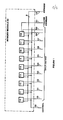
- Figure 1 is seen the electrical block diagram of the invention.
- eight individual memory chips 10-17 each capable of storing a zero or a one binary bit at each memory location, are accessed by a multi-bit address applied to address leads 19 which comprises eight leads.
- address leads 19 which comprises eight leads.
- single input/output leads 20-27 are provided respectively to each of memory chips 10-17 to provide a total of eight input/output leads making up an eight bit binary word.
- Control lead 29 connected to one input of each of memory chips 10-17 on the module 30 indicates whether a read or write operation is be performed at the location identified by the address present on the eight address leads 19 which are interconnected to the addressing inputs of each of chips 10-17.
- an extra memory chip 18 similarly connected in parallel with memory chips 10-17, the read/ write control leads of which are interconnected with the control leads 29 connected to memory chips 10-17 with the exception of the column address select lead 31.
- Memory chip 18 has a data input lead 28 and a separate data output lead 32 as distinguished from memory chips 10-17 which respectively use common input/output data leads 20-27 for both data input and output.
- a total of ten input/output data leads 20-28 and 32 are therefore provided on the edge of the memory module 30 as shown and eight bit binary words plus and extra ninth bit for functions such as parity checking are stored in or read out of the memory module 30.
- a separate column address select lead 31 is provided for memory chip 18 to enable independent operation for the parity function.
- the binary bits are applied to terminals on the edge of memory module 30 which are connected to common input/output leads 20-27 and to input lead 28. Each of the nine binary bits is thereby applied to the input respectively of memory chips 10-18. A signal is then applied to control lead 29 at a terminal on the edge of memory module 30, which control lead 29 is connected to the read/write control input of chips 10-18. Finally, a multibit binary address is applied to the multiple address leads 19 also on the edge of memory module 30, which addressing leads are connected to the addressing inputs of each of memory chips 10-18. In response to all the above signals applied to the appropriate terminals of memory module 30, the binary word on input/output leads 20-27 and the extra binary bit on input lead 28 are stored respectively in memory chips 10-17 and 18 at the address indicated by the binary number on address leads 19.
- a read signal is applied to read/write control lead 29 and a binary address is applied to address leads 19.
- a binary address is applied to address leads 19.
- the binary word stored in memory module 30 at the indicated address is read out of memory chips 10-17 and 18 respectively onto input/output leads 20-27 and output lead 32.
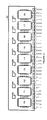
- module 30 there is shown a physical layout of the memory module 30.
- the nine memory chips 10-18 are mounted on a substrate 31 that may be printed circuit board or ceramic.
- the memory chips 10-18 may be dynamic RAMs (D-RAM) advantageously packaged in small plastic leaded chip carriers.
- D-RAM dynamic RAMs
- small ceramic decoupling capacitors 33-40 mounted on the substrate of module 30 , having a value between 0,1 and 0,22 ufd, and connected between each of memory chips 10-18 to suppress transient voltage spikes.
- module 30 may have physical dimensions in the order of three-quarter inch by three inches while providing large memory capacity. Sixty-four thousand words on the module are presently possible and two hundred fifty-six thousand bytes are feasible with the physical dimensions of module 30 only being slightly larger.
- module 30 the input, output and control of the memory elements 10-18 on module 30 may be accomplished via only thirty terminals on the edge of the module.
- Use of module 30 in lieu of memory chips in conventional dual in line terminal packages normally mounted in rows and columns on a printed circuit board enables an eight-fold density increase over previous circuit assembly technology.
- the unpackaged dies may be mounted on a substrate to implement the invention in a hybrid integrated circuit package or in a large scale integrated circuit package.
Landscapes
- Engineering & Computer Science (AREA)
- Theoretical Computer Science (AREA)
- General Physics & Mathematics (AREA)
- Physics & Mathematics (AREA)
- Power Engineering (AREA)
- General Engineering & Computer Science (AREA)
- Quality & Reliability (AREA)
- Microelectronics & Electronic Packaging (AREA)
- Condensed Matter Physics & Semiconductors (AREA)
- Computer Hardware Design (AREA)
- Techniques For Improving Reliability Of Storages (AREA)
- Semiconductor Memories (AREA)
- For Increasing The Reliability Of Semiconductor Memories (AREA)
Abstract
A memory module to and from which multibit binary words are stored and read out. Each multibit binary word comprises a standard word size and another memory bit that may be used for purposes such as parity checking. The modules may be mounted on a printed circuit mother board from which power, control signals and binary words are applied to and taken from the module.
Description
- The present invention is concerned with a memory module with a plurality of memory chips arranged on mounting means. Multibit binary words are stored and read out. Each multibit binary word comprises a standard byte size and one or more other memory bits that may be used for purposes such as parity checking. The modules may be mounted on a printed circuit mother board from which power, control signals and binary words are applied to and taken from the module.
- It is an object of the invention to provide a memory module with memory components having their power, control, input/output and other access leads interconnected so that there is only one set of these leads available at terminals of the module. Especially the number of terminals of the module should be reduced and the information density should be increased over previous circuit assemblies.
- A solution of these problems is characterized in the claims.
- The present invention is a memory module on which a plurality of memory components each storing or reading one binary bit at a time have their power, control, input/output and other access leads interconnected so there is only one set of these leads available at terminals of the module. A first plurality of these memories provide for one binary word being input or output to the memory module at a time. In addition, it is added another individual memory intended for purposes such as parity checking and error correction. This additional memory has its power and control leads interconnected with the other memories within the module, but has separate input/output lead(s) and column address select leads to enable independent accessing or addressing of the parity memory.
- The invention will be understood on reading the following detailed description in conjuction with the drawing in which:
- Fig. 1 is an electrical block diagram of the novel memory module; and
- Fig. 2 is a mechanical layout drawing of the memory module.
- In Figure 1 is seen the electrical block diagram of the invention. In one embodiment of the invention, the embodiment shown in Fig. 1, eight individual memory chips 10-17, each capable of storing a zero or a one binary bit at each memory location, are accessed by a multi-bit address applied to
address leads 19 which comprises eight leads. With this embodiment of the invention, single input/output leads 20-27 are provided respectively to each of memory chips 10-17 to provide a total of eight input/output leads making up an eight bit binary word.Control lead 29 connected to one input of each of memory chips 10-17 on themodule 30 indicates whether a read or write operation is be performed at the location identified by the address present on the eight address leads 19 which are interconnected to the addressing inputs of each of chips 10-17. - In a manner well known in the art the concurrent addressing and control of chips 10-17 which are connected in parallel permits an eight bit byte or binary word to be stored in or read out of memory chips 10-17 for each read or write operation.
- In accordance with the preferred embodiment of the invention it is provided an
extra memory chip 18 similarly connected in parallel with memory chips 10-17, the read/ write control leads of which are interconnected with the control leads 29 connected to memory chips 10-17 with the exception of the column addressselect lead 31.Memory chip 18 has adata input lead 28 and a separatedata output lead 32 as distinguished from memory chips 10-17 which respectively use common input/output data leads 20-27 for both data input and output. A total of ten input/output data leads 20-28 and 32 are therefore provided on the edge of thememory module 30 as shown and eight bit binary words plus and extra ninth bit for functions such as parity checking are stored in or read out of thememory module 30. A separate column addressselect lead 31 is provided formemory chip 18 to enable independent operation for the parity function. - When it is desired to store a binary word made up of an eight bit byte/word with a ninth parity bit in a specific address location in memory chips 10-17 and 18, the binary bits are applied to terminals on the edge of
memory module 30 which are connected to common input/output leads 20-27 and to inputlead 28. Each of the nine binary bits is thereby applied to the input respectively of memory chips 10-18. A signal is then applied tocontrol lead 29 at a terminal on the edge ofmemory module 30, whichcontrol lead 29 is connected to the read/write control input of chips 10-18. Finally, a multibit binary address is applied to the multiple address leads 19 also on the edge ofmemory module 30, which addressing leads are connected to the addressing inputs of each of memory chips 10-18. In response to all the above signals applied to the appropriate terminals ofmemory module 30, the binary word on input/output leads 20-27 and the extra binary bit oninput lead 28 are stored respectively in memory chips 10-17 and 18 at the address indicated by the binary number on address leads 19. - Similarly, when it is desired to read a binary word out of
memory module 30, a read signal is applied to read/writecontrol lead 29 and a binary address is applied toaddress leads 19. In response thereto, the binary word stored inmemory module 30 at the indicated address is read out of memory chips 10-17 and 18 respectively onto input/output leads 20-27 andoutput lead 32. - Referring to Figure 2, there is shown a physical layout of the
memory module 30. The nine memory chips 10-18 are mounted on asubstrate 31 that may be printed circuit board or ceramic. The memory chips 10-18 may be dynamic RAMs (D-RAM) advantageously packaged in small plastic leaded chip carriers. Also mounted on the substrate ofmodule 30 are small ceramic decoupling capacitors 33-40, having a value between 0,1 and 0,22 ufd, and connected between each of memory chips 10-18 to suppress transient voltage spikes. By using the small D-RAMs and small capacitors,module 30 may have physical dimensions in the order of three-quarter inch by three inches while providing large memory capacity. Sixty-four thousand words on the module are presently possible and two hundred fifty-six thousand bytes are feasible with the physical dimensions ofmodule 30 only being slightly larger. - With the invention the input, output and control of the memory elements 10-18 on
module 30 may be accomplished via only thirty terminals on the edge of the module. Use ofmodule 30 in lieu of memory chips in conventional dual in line terminal packages normally mounted in rows and columns on a printed circuit board enables an eight-fold density increase over previous circuit assembly technology. - In addition, by having an extra memory chip parity may be checked. By having separate control of the extra memory chip a system designer has more flexibility in designing parity operation.
- While what has been described hereinabove is the preferred embodiment of the invention, it will be obious to those skilled in the art that numerous changes may be made without departing from the spirit or scope of the invention. More than one bit may be used for parity checking or other purposes. In addition, rather than using discrete memory chips, the unpackaged dies may be mounted on a substrate to implement the invention in a hybrid integrated circuit package or in a large scale integrated circuit package.
Claims (3)
1. A memory module comprising a plurality of memory chips arranged on mounting means
characterized in
that control inputs (19, 29) of a first plurality of memory chips are interconnected by the mounting means so that one word of digital information may be input or output from said memory chips at a time, said mounting means (30) including terminal means (FIG. 2) for providing access to said input, output (20-27) and control inputs (19, 29) of said first plurality of memory chips to thereby enable reading and writing said words of digital information into and out of said first plurality of memory chips, and an auxiliary memory chip (18) for storing error correction and detection information, said auxiliary memory chip (18) being mounted on said mounting means (30) and having its control inputs interconnected with the control inputs of said first plurality of memory chips (10-17).
2. A memory module comprising a plurality of memory chips arranged on mounting means
characterized in
that a first plurality of data memory chips (10-17) each having data input/output (20-27), read/write (29) and. addressing control inputs (19), mounting means (30) for mounting said first plurality of memory chips (10-17) and interconnecting the read/write (29) and addressing (19) control inputs of said first plurality of memory chips (10-17) so that one word of digital information may be written into or read out from said first plurality of memory chips (10-17) at a time, said mounting means (30) including terminal means for providing connection to said (input/output (27), read/write (29) and addressing control (19) inputs of each of said first plurality of memory chips (10-17) to thereby enable reading and writing said words of digital information into and out of said first plurality of memory chips (10-17) and auxiliary memory means (18) for storing information ancilliary to said words of digital information, said auxiliary memory means (18) being mounted on said mounting means (30) and having read/write inputs that are interconnected with the read/write inputs of said first plurality of memory chips (10-17), and said auxiliary memory means (18) having an addressing control input (31) that is accessable via said terminal means to provide flexibility in reading and writing said ancilliary information.
3. The invention in accordance with claim 2 characterized in that
said auxiliary memory means (18) comprises an auxiliary memory chip for storing error correction and detection information which may written into or read out of said auxiliary memory chip (18) at times other than when said words of digital information are written into or read out of said first plurality of memory chips (10-17) to thereby facilitate said error detection and correction operation.
said auxiliary memory means (18) comprises an auxiliary memory chip for storing error correction and detection information which may written into or read out of said auxiliary memory chip (18) at times other than when said words of digital information are written into or read out of said first plurality of memory chips (10-17) to thereby facilitate said error detection and correction operation.
Applications Claiming Priority (2)
| Application Number | Priority Date | Filing Date | Title |
|---|---|---|---|
| US52881783A | 1983-09-02 | 1983-09-02 | |
| US528817 | 1983-09-02 |
Publications (1)
| Publication Number | Publication Date |
|---|---|
| EP0135821A2 true EP0135821A2 (en) | 1985-04-03 |
Family
ID=24107312
Family Applications (1)
| Application Number | Title | Priority Date | Filing Date |
|---|---|---|---|
| EP84110137A Withdrawn EP0135821A2 (en) | 1983-09-02 | 1984-08-24 | Memory module |
Country Status (5)
| Country | Link |
|---|---|
| EP (1) | EP0135821A2 (en) |
| JP (1) | JPS6072049A (en) |
| CA (1) | CA1232355A (en) |
| DE (1) | DE8422792U1 (en) |
| GB (1) | GB2146148A (en) |
Cited By (1)
| Publication number | Priority date | Publication date | Assignee | Title |
|---|---|---|---|---|
| FR2645320A1 (en) * | 1989-03-31 | 1990-10-05 | Gen Electric Cgr | COMPACT MEMORY MODULE FOR DATA MEMORY CARD OF AN IMAGE PROCESSOR |
Families Citing this family (2)
| Publication number | Priority date | Publication date | Assignee | Title |
|---|---|---|---|---|
| KR100335504B1 (en) * | 2000-06-30 | 2002-05-09 | 윤종용 | 2 Channel memory system having shared control and address bus and memory modules used therein |
| JP2012177964A (en) * | 2011-02-25 | 2012-09-13 | Nec Computertechno Ltd | Memory system and memory module control method |
Family Cites Families (9)
| Publication number | Priority date | Publication date | Assignee | Title |
|---|---|---|---|---|
| GB1439333A (en) * | 1972-09-16 | 1976-06-16 | Plessey Co Ltd | Electronic multi-register arrangements |
| DE2549392C3 (en) * | 1975-11-04 | 1978-07-27 | Siemens Ag, 1000 Berlin Und 8000 Muenchen | Method for increasing the reliability of integrated memory modules and for improving the yield of memory modules that appear to be error-free from the outside during their manufacture |
| GB2003302B (en) * | 1977-08-24 | 1982-02-10 | Ncr Co | Random access memory system |
| IT1108375B (en) * | 1978-03-09 | 1985-12-09 | Cselt Centro Studi Lab Telecom | SOLID STATE GROUND MEMORY WITH SELF-CORRECTION AND ORGANIZED IN WORDS FOR A REGISTERED PROGRAM CONTROL SYSTEM |
| IT1109655B (en) * | 1978-06-28 | 1985-12-23 | Cselt Centro Studi Lab Telecom | SOLID STATE GROUND MEMORY ORGANIZED WITH SELF-CORRECTIVE BIT AND RECONFIGURABLE FOR A REGISTERED PROGRAM CONTROL SYSTEM |
| US4319356A (en) * | 1979-12-19 | 1982-03-09 | Ncr Corporation | Self-correcting memory system |
| JPS5737799A (en) * | 1980-08-19 | 1982-03-02 | Nec Corp | Storage device |
| IT1142074B (en) * | 1981-11-24 | 1986-10-08 | Honeywell Inf Systems | DATA PROCESSING SYSTEM WITH AUTOMATIC ALLOCATION OF THE ADDRESS IN A MODULAR MEMORY |
| JPH07117198A (en) * | 1993-10-25 | 1995-05-09 | Mitsubishi Chem Corp | Polyamide laminated biaxial oriented film |
-
1984
- 1984-07-16 CA CA000458952A patent/CA1232355A/en not_active Expired
- 1984-07-17 GB GB08418183A patent/GB2146148A/en not_active Withdrawn
- 1984-07-31 DE DE19848422792U patent/DE8422792U1/en not_active Expired
- 1984-08-24 EP EP84110137A patent/EP0135821A2/en not_active Withdrawn
- 1984-08-30 JP JP59181622A patent/JPS6072049A/en active Pending
Cited By (2)
| Publication number | Priority date | Publication date | Assignee | Title |
|---|---|---|---|---|
| FR2645320A1 (en) * | 1989-03-31 | 1990-10-05 | Gen Electric Cgr | COMPACT MEMORY MODULE FOR DATA MEMORY CARD OF AN IMAGE PROCESSOR |
| EP0392892A1 (en) * | 1989-03-31 | 1990-10-17 | General Electric Cgr S.A. | Compact memory module for data memory card of an image processor |
Also Published As
| Publication number | Publication date |
|---|---|
| CA1232355A (en) | 1988-02-02 |
| AU2909384A (en) | 1985-03-07 |
| GB2146148A (en) | 1985-04-11 |
| DE8422792U1 (en) | 1985-01-17 |
| GB8418183D0 (en) | 1984-08-22 |
| JPS6072049A (en) | 1985-04-24 |
| AU565040B2 (en) | 1987-09-03 |
Similar Documents
| Publication | Publication Date | Title |
|---|---|---|
| US4727513A (en) | Signal in-line memory module | |
| US4656605A (en) | Single in-line memory module | |
| US5164916A (en) | High-density double-sided multi-string memory module with resistor for insertion detection | |
| KR100220000B1 (en) | Memory module arranged for data and parity bits | |
| KR100626223B1 (en) | A memory expansion module with stacked memory packages | |
| US4443864A (en) | Memory system for microprocessor with multiplexed address/data bus | |
| US4545010A (en) | Memory identification apparatus and method | |
| EP0016827B1 (en) | High density memory system | |
| US20040186948A1 (en) | Device and method for controlling solid-state memory system | |
| US4306298A (en) | Memory system for microprocessor with multiplexed address/data bus | |
| EP0264893A3 (en) | Semiconductor memory | |
| EP0374829A2 (en) | Dual port memory unit | |
| US3967251A (en) | User variable computer memory module | |
| EP0808486A2 (en) | Parallel processing redundancy scheme for faster access times and lower die area | |
| US5367526A (en) | Memory module, parity bit emulator, and associated method for parity bit emulation | |
| IT1002271B (en) | IMPROVEMENT TO PARITY CONTROL DEVICES IN SEMICONDUCTOR MEMORIES | |
| US5064378A (en) | Mounting of DRAMs of different sizes and pinouts within limited footprint | |
| EP0135821A2 (en) | Memory module | |
| US6147924A (en) | Arrangement of data input/output circuits for use in a semiconductor memory device | |
| CN104254889A (en) | Packaged memory dies that share a chip select line | |
| USH1915H (en) | Hybrid static RAM circuit | |
| JPS6233625B2 (en) | ||
| US5337286A (en) | Semiconductor memory device | |
| WO1997027593A1 (en) | Stacked memory module substrate and system for accessing the substrate | |
| JPS5882351A (en) | Memory device |
Legal Events
| Date | Code | Title | Description |
|---|---|---|---|
| PUAI | Public reference made under article 153(3) epc to a published international application that has entered the european phase |
Free format text: ORIGINAL CODE: 0009012 |
|
| AK | Designated contracting states |
Designated state(s): BE DE FR |
|
| STAA | Information on the status of an ep patent application or granted ep patent |
Free format text: STATUS: THE APPLICATION IS DEEMED TO BE WITHDRAWN |
|
| 18D | Application deemed to be withdrawn |
Effective date: 19860902 |
|
| RIN1 | Information on inventor provided before grant (corrected) |
Inventor name: CLAYTON, JAMES ELLIOTT |