EP0117719A2 - Méthode pour décoder un signal vidéo codé et dispositif récepteur pour décoder le signal - Google Patents
Méthode pour décoder un signal vidéo codé et dispositif récepteur pour décoder le signal Download PDFInfo
- Publication number
- EP0117719A2 EP0117719A2 EP84301147A EP84301147A EP0117719A2 EP 0117719 A2 EP0117719 A2 EP 0117719A2 EP 84301147 A EP84301147 A EP 84301147A EP 84301147 A EP84301147 A EP 84301147A EP 0117719 A2 EP0117719 A2 EP 0117719A2
- Authority
- EP
- European Patent Office
- Prior art keywords
- signal
- video signal
- identification
- decoding
- level
- Prior art date
- Legal status (The legal status is an assumption and is not a legal conclusion. Google has not performed a legal analysis and makes no representation as to the accuracy of the status listed.)
- Granted
Links
Images


Classifications
-
- H—ELECTRICITY
- H04—ELECTRIC COMMUNICATION TECHNIQUE
- H04N—PICTORIAL COMMUNICATION, e.g. TELEVISION
- H04N5/00—Details of television systems
- H04N5/76—Television signal recording
- H04N5/91—Television signal processing therefor
- H04N5/913—Television signal processing therefor for scrambling ; for copy protection
-
- H—ELECTRICITY
- H04—ELECTRIC COMMUNICATION TECHNIQUE
- H04N—PICTORIAL COMMUNICATION, e.g. TELEVISION
- H04N7/00—Television systems
- H04N7/16—Analogue secrecy systems; Analogue subscription systems
- H04N7/167—Systems rendering the television signal unintelligible and subsequently intelligible
- H04N7/171—Systems operating in the amplitude domain of the television signal
- H04N7/1716—Systems operating in the amplitude domain of the television signal by inverting the polarity of active picture signal portions
-
- H—ELECTRICITY
- H04—ELECTRIC COMMUNICATION TECHNIQUE
- H04N—PICTORIAL COMMUNICATION, e.g. TELEVISION
- H04N5/00—Details of television systems
- H04N5/76—Television signal recording
- H04N5/91—Television signal processing therefor
- H04N5/913—Television signal processing therefor for scrambling ; for copy protection
- H04N2005/91357—Television signal processing therefor for scrambling ; for copy protection by modifying the video signal
- H04N2005/91364—Television signal processing therefor for scrambling ; for copy protection by modifying the video signal the video signal being scrambled
Definitions
- the present invention relates to an encoded video signal and, more particularly, to a method for broadcasting an encoded video signal and to receiving apparatus for decoding the video signal.
- a video signal can be encoded before broadcasting to prevent the use of the video signal unless the coding technique is known.
- Certain "pay-TV" systems are based on the payment of a fee for a device that is programmed for the particular coding technique being used so that the received signal can be used to generate a television picture.
- VTR video tape recorder
- an encoded video signal can be broadcast with a scrambled portion encoded prior to broadcasting using an encoding axis at a predetermined reference level and first and second identification signals in consecutive horizontal periods of the video signal at substantially the same identification level in both of the periods.
- the reference level and the identification level have a predetermined relationship.
- the signal is decoded at a receiving apparatus by detecting the level of the second identification signal and generating in response to that level a decoding axis at the reference level which was used to encode the signal.
- the present invention can best be understood by first having an understanding of video signal encoding techniques and how prior art VTR noise reduction circuits interfere with the proper functioning of those techniques.
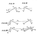
- FIG. 1A shows a portion of an original video signal.
- the portion depicted includes a horizontal synchronizing pulse SYNC and a video information portion S immediately following the SYNC pulse, which together form a horizontal scanning period of the video signal.
- the end of that horizontal period is defined by another horizontal synchronizing pulse, SYNC, which begins the next horizontal scanning period of the signal.
- FIG. 1B illustrates the same video signal encoded prior to being broadcast.
- the signal portion S is scrambled by inverting it about an encoding axis M e at a predetermined reference level V to provide the scrambled portion of the video signal S vs shown in FIG. 1B.
- the reference level V is chosen relative to the pedestal level of the signal immediately proceeding or following the SYNC pulse.
- the SYNC pulses are not inverted because to do so would make the restoration of the signal unnecessarily complicated.
- the entire video signal includes non-inverted portions arranged in a predetermined pattern with inverted portions.
- "Key codes” and other information are also included in the signal for use by the receiver to detect the encoding technique, thus enabling the signal to be unscrambled.
- the scrambled portions will include inverted and non-inverted vertical intervals of the signal arranged in a pattern that is detectable at the receiver by using the coding information.
- the receiver provides a decoding axis M d at the reference level V m and inverts the received signal S vs back to its original form S v , as shown in FIG. 2A.
- errors in setting the reference level at the receiver can occur.
- electronic components in the receiver may have characteristics that cannot be precisely controlled, for example, because of ambient temperature fluctuations.
- the reference level V m can be off by an amount such as ⁇ V m shown in FIG. 2B, resulting in an erroneously unscrambled signal.
- the decoding axis is set at V instead of V m , and inversion about that axis results in the signal S v ' instead of the correct signal S v shown in the dash line in FIG. 2B.
- the vertical blanking interval of the video signal portion depicted in FIG. 3 has an identifi- cation signal ID included in the sixteenth horizontal period.
- the scrambled portion S vs of the signal is also shown in FIG. 3.
- the identification signal ID is broadcast at a predetermined identification level V ' above the pedestal level of the signal.
- the identification level has a known value relative to the reference level V m (in FIG. 3 they are the same). Since the identification level V m ' will change under the same influences as the reference level V m , and the identification level is detectable at the receiver by sampling the identification signal ID, the reference level V m can be accurately set regardless of conditions at the receiver.
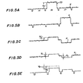
- FIG. 4 shows a prior art noise reduction circuit used in conventional VTR's.
- the noise reduction circuit accepts the video signal Y and provides it to a main circuit path and to a parallel circuit path which includes a delay circuit 1.
- the delay circuit 1 accepts the main signal a and provides it as a delayed signal b delayed by the time of one horizontal scanning period 1H.
- the delayed signal b is subtracted from the main signal a by a subtracting circuit 2 in the parallel circuit path.
- the level of the signal appearing at the output of the subtracting circuit 2 is divided in half by a dividing circuit 3 to produce the divided signal c.
- the divided signal c passes through a limiter 4 in the parallel circuit path to clip the portion of the divided signal c above a certain level and provide a clipped signal d.
- the clipped signal d is subtracted from the main signal a by a subtracting circuit 5 in the main circuit path to provide the output signal e, which is a modified signal Y' having less noise than the main signal a
- FIGS. 5A-5E illustrate how the noise reduction circuit shown in FIG. 4 operates.
- the letter suffixes used to identify FIGS. 5A-5E correspond to the signals a through e discussed in connection with FIG. 4.
- Part of the vertical blanking portion of the received video signal after demodulation is shown in FIG. 5A. It includes the identification signal ID in the sixteenth horizontal period.
- a noise component N is shown superimposed on the signal.
- the delayed signal b shown in FIG. 5B has an orientation relative to the main signal a as shown by comparing FIGS. 5A and SB.
- the divided signal c appears as shown in FIG. SC.
- the limiter 4 clips the signal c at the level V and the clipped signal d has the waveform shown in FIG. 5D.
- the output signal e results.
- the noise component N is significantly reduced in all portions of the signal except in the identification signal ID. But the presence and timing of the identification signal ID remains recoverable even when combined with the noise component, so that for those purposes it is not critical that the identification signal be subject to noise reduction.
- the operation of the noise reduction circuit is best understood mathematically.
- the signal a can be expressed:
- the divided signal c is equation (1) subtracted from equation (2) and divided by two: Other than at the identification portion ID, S - S D , so that At the portions of the signal represented by equation (4), the limiter circuit 4 has no effect if the clipping level V e is greater than the largest noise component.
- Y d Y c for those portions.
- Equation (6) Although it would appear from equation (6) that there has been no reduction in the noise level of the signal, the effect of the noise component changes as the square of the noise level. Thus, if the total noise in equation (6) is expressed: then the effect of each component on the signal Y' can be expressed as ⁇ 1 ⁇ 2N 2 + 1 ⁇ 4N D 2 , or, if N is assumed to be approximately equal to N D , then the effect of the noise component is 1 ⁇ 2N 2 . Thus, the modified, reduced-noise signal Y' effectively has only half as much noise at all portions other than at the identification signal ID. There, the signal still has the same amount of noise since the noise component was removed by the limiter 4.
- V m ' the effect of the noise reduction circuit on the identification level V ' is depicted in FIG. 5E.
- V m ' is now changed by the amount V e .
- V m ' no longer can be used to derive the reference level V m for generating the decoding axis to decode the signal.
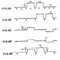
- the video signal of the present invention uses an identification signal ID having substantially the same level in two consecutive horizontal periods, as shown in FIG. 6.
- the broadcast and received signal has a first identification signal ID 1 in the 15th horizontal period and a second identification signal ID 2 in the 16th horizontal period of a vertical blanking interval.
- the letter suffixes in FIGS. 6A-6E correspond with the signals a through e as discussed in connection with FIGS. 4 and 5A-5E.
- the signal After passing through the delay circuit 1, the signal has the waveform shown in FIG. 6B. As shown in FIGS.
- the divided signal c and the clipped signal d have a 16th horizontal period (relative to the main signal a) which is at the same level as that obtained when two periods without identification signals are subtracted in the subtracting circuit 2.
- the portion of the clipped signal d corresponding to the 16th horizontal scanning period of the main signal a is zero.
- the level of the identification signal ID 2 which was V ' when received, is still V ' after the m signal passes through the noise reduction circuit, as seen in FIG. 6E.
- the decoding axis can thus be accurately set at the reference level V even though the signal has been subject to noise reduction.
- key codes were included in other consecutive horizontal periods, they could also be recovered unchanged by the noise reduction circuit.
- FIG. 7 schematically illustrates a video signal receiving apparatus which includes a decoding circuit 10 for unscrambling the signal depicted in FIG. 6E.
- a VTR 11 receives a broadcast signal from an antenna 12.
- the received signal is provided to a tuner 13 and from the tuner 13 to a detector 14.
- the detector 14 provides a signal to a recording circuit 15 which, in the conventional manner, frequency modulates the luminance portion of the composite video signal and converts the chrominance portion to a lower frequency.
- the signal from the recording circuit 15 is supplied to the record terminal REC of a switch 16.
- the switch 16 provides a circuit path through the terminal REC, the received signal is supplied to a magnetic head 17 for recording on the tape 18.
- the switch 16 When the recorded signal is reproduced, the switch 16 provides a circuit path through a playback terminal P B .
- the reproduced signal is supplied to a reproducing circuit 19 that demodulates the luminance portion and converts the chrominance portion to the original higher frequency.
- the reproduced signal is supplied to a VTR output terminal 20.
- the decoding circuit 10 has an input terminal 21 that accepts the composite video signal.
- the composite signal is supplied to a clamping circuit 22, a pulse separating circuit 23 and a key code detector 24.
- the output of the pulse separating circuit 23 is supplied to a sampling pulse generator 25.
- the sampling pulse therefrom is fed to a sampling circuit 26, which also accepts the output of the clamping circuit 22.
- a decoding axis generator 27 accepts the output of the sampling circuit 26 and provides a signal to an inverting circuit 28.
- the inverting circuit 28 accepts the output of the clamping circuit 22 and, using the output of the decoding axis generator 27, inverts the output of the clamping circuit 22 about the decoding axis.
- the output of the key code detector 24 is supplied to a switching circuit 29, the output of which is fed to a switch 30.
- the switching circuit 29 controls the switch 30 in response to the key code supplied by the key code detector 24 and the output of the sampling circuit 26.
- the switch 30 comprises two fixed terminals t a and t b and a movable terminal t.
- the switch 30, as controlled by the switching circuit 29 provides a circuit path between the terminals t a and t
- the composite signal, as reproduced is provided directly to the terminal t c .
- the circuit 29 provides a circuit path between the terminals t b and t c
- the output of the inverting circuit 28 is supplied to the terminal t c .
- a buffer amplifier 31 accepts the signal at the terminal t and provides an output to the output terminal 32 of the decoding circuit 10.
- the signal at the output terminal 32 is used to generate a television picture by conventional means.
- the decoding circuit 10 operates as follows.
- the clamping circuit 22 clamps the pedestal level of the composite signal from the reproducing circuit 19.
- the horizontal and vertical synchronizing pulses in the video signal are extracted by the pulse separating circuit 23.
- the sampling pulse generator 25 uses the horizontal and vertical synchronizing pulses provided by the pulse generating circuit 23 to provide a sampling pulse for each horizontal interval containing the second identification signal ID 2 , the identification level V m ' of which, it will be recalled, was unaffected by the noise reduction circuit.
- the horizontal interval to be sampled is known, and the sampling pulse generator 25 provides a pulse for sampling that interval.
- the sampling circuit 26 uses that sampling pulse to sample the proper portion of the level of the video signal from the clamping circuit 22.
- the level which is sampled is that of the second identification signal ID 2 and the output of the sampling circuit 26 is at the identification level V m '.
- the output of the pulse separating circuit 23 is also supplied to the key code detector 24.
- the key code detector 24 uses the output of the pulse separating circuit 23 to locate the key code in the video signal from the VTR and supply to the switching circuit 29 a code signal in response to the key code.
- the switching circuit 29 also accepts the identification signal ID 2 , which functions as a timing signal for the switching circuit 29.
- the switching circuit 29 uses the identification signal and the key code to provide a switching signal at the proper times depending on the horizontal intervals where the signal was inverted.
- the identification level V m ' is used by the decoding axis generator 27 to generate the reference level V m about which the broadcast signal was inverted.
- the signal from the clamping circuit 22 is inverted about that decoding axis before being supplied to the switch terminal t b .
- the switch 30, as controlled by the switching circuit 29, provides a circuit path for the restored video signal from the inverting circuit 28 at the horizontal periods in which the video signal was inverted. Otherwise, the switch 30 provides a circuit path in which the video signal is supplied directly to the buffer amplifier 31 from the clamping circuit 22.
- the signal supplied to the output terminal 32 of the decoder 10 is identical to the original signal that was scrambled prior to broadcasting.
- the decoding circuit 10 can be by-passed so that the output of the reproducing circuit 19 is used directly to generate a televison picture if the recorded signal was not encoded on broadcasting.
- the decoding circuit 10 can be automatically included and excluded from the receiver by using the existence or absence of the identification signal ID as an indication that the recorded signal was encoded. If an identification signal is present, the video signal is supplied to the terminal 21. If not, it is supplied directly to the means for generating the television picture.
- the video signal and the decoding apparatus of the present invention enable proper decoding of a recorded, video signal when it is played back, even when a noise reduction circuit is used in the recording apparatus.
Applications Claiming Priority (2)
| Application Number | Priority Date | Filing Date | Title |
|---|---|---|---|
| JP28879/83 | 1983-02-23 | ||
| JP58028879A JPS59154887A (ja) | 1983-02-23 | 1983-02-23 | 映像信号受信装置 |
Publications (3)
| Publication Number | Publication Date |
|---|---|
| EP0117719A2 true EP0117719A2 (fr) | 1984-09-05 |
| EP0117719A3 EP0117719A3 (en) | 1987-08-26 |
| EP0117719B1 EP0117719B1 (fr) | 1991-10-16 |
Family
ID=12260672
Family Applications (1)
| Application Number | Title | Priority Date | Filing Date |
|---|---|---|---|
| EP84301147A Expired - Lifetime EP0117719B1 (fr) | 1983-02-23 | 1984-02-22 | Méthode pour décoder un signal vidéo codé et dispositif récepteur pour décoder le signal |
Country Status (7)
| Country | Link |
|---|---|
| US (1) | US4613902A (fr) |
| EP (1) | EP0117719B1 (fr) |
| JP (1) | JPS59154887A (fr) |
| AU (1) | AU559380B2 (fr) |
| BR (1) | BR8400809A (fr) |
| CA (1) | CA1219059A (fr) |
| DE (1) | DE3485157D1 (fr) |
Cited By (1)
| Publication number | Priority date | Publication date | Assignee | Title |
|---|---|---|---|---|
| AU629548B2 (en) * | 1988-05-25 | 1992-10-08 | Sony Corporation | Apparatus for decoding a digital signal |
Families Citing this family (5)
| Publication number | Priority date | Publication date | Assignee | Title |
|---|---|---|---|---|
| JPS6190586A (ja) * | 1984-10-09 | 1986-05-08 | Alps Electric Co Ltd | 映像信号生成回路 |
| US4716588A (en) * | 1985-10-29 | 1987-12-29 | Payview Limited | Addressable subscription television system having multiple scrambling modes |
| US4924498A (en) * | 1988-04-29 | 1990-05-08 | Scientific Atlanta, Inc. | Method and apparatus for improving video scrambling and employing split snyc pulses |
| US5177787A (en) * | 1989-05-01 | 1993-01-05 | Scientific-Atlanta, Inc | Scrambler with self-calibration |
| EP0431875A3 (en) * | 1989-12-04 | 1992-02-26 | Matsushita Electric Industrial Co., Ltd. | Energy dispersal signal adding apparatus and energy dispersal signal removing apparatus |
Citations (6)
| Publication number | Priority date | Publication date | Assignee | Title |
|---|---|---|---|---|
| US3440338A (en) * | 1963-11-15 | 1969-04-22 | Teleglobe Pay Tv System Inc | Subscription television system |
| US3824332A (en) * | 1972-02-18 | 1974-07-16 | I Horowitz | Pay television system |
| US3919462A (en) * | 1973-08-15 | 1975-11-11 | System Dev Corp | Method and apparatus for scrambling and unscrambling communication signals |
| GB2042846A (en) * | 1979-02-20 | 1980-09-24 | Payview Ltd | Secret television |
| US4257065A (en) * | 1979-12-17 | 1981-03-17 | Pay Television Corporation | Video clamp and inverter circuit |
| US4340906A (en) * | 1980-05-14 | 1982-07-20 | Oak Industries Inc. | Video signal coding by video signal polarity reversal on the basis of brightness level comparison |
Family Cites Families (1)
| Publication number | Priority date | Publication date | Assignee | Title |
|---|---|---|---|---|
| US4511919A (en) * | 1981-12-01 | 1985-04-16 | Hamlin International Corp. | Method and apparatus for scrambling and descrambling video signals in a multichannel system |
-
1983
- 1983-02-23 JP JP58028879A patent/JPS59154887A/ja active Granted
-
1984
- 1984-02-17 CA CA000447665A patent/CA1219059A/fr not_active Expired
- 1984-02-22 EP EP84301147A patent/EP0117719B1/fr not_active Expired - Lifetime
- 1984-02-22 AU AU24815/84A patent/AU559380B2/en not_active Ceased
- 1984-02-22 DE DE8484301147T patent/DE3485157D1/de not_active Expired - Lifetime
- 1984-02-22 BR BR8400809A patent/BR8400809A/pt not_active IP Right Cessation
- 1984-02-23 US US06/582,816 patent/US4613902A/en not_active Expired - Lifetime
Patent Citations (6)
| Publication number | Priority date | Publication date | Assignee | Title |
|---|---|---|---|---|
| US3440338A (en) * | 1963-11-15 | 1969-04-22 | Teleglobe Pay Tv System Inc | Subscription television system |
| US3824332A (en) * | 1972-02-18 | 1974-07-16 | I Horowitz | Pay television system |
| US3919462A (en) * | 1973-08-15 | 1975-11-11 | System Dev Corp | Method and apparatus for scrambling and unscrambling communication signals |
| GB2042846A (en) * | 1979-02-20 | 1980-09-24 | Payview Ltd | Secret television |
| US4257065A (en) * | 1979-12-17 | 1981-03-17 | Pay Television Corporation | Video clamp and inverter circuit |
| US4340906A (en) * | 1980-05-14 | 1982-07-20 | Oak Industries Inc. | Video signal coding by video signal polarity reversal on the basis of brightness level comparison |
Cited By (1)
| Publication number | Priority date | Publication date | Assignee | Title |
|---|---|---|---|---|
| AU629548B2 (en) * | 1988-05-25 | 1992-10-08 | Sony Corporation | Apparatus for decoding a digital signal |
Also Published As
| Publication number | Publication date |
|---|---|
| BR8400809A (pt) | 1984-10-02 |
| DE3485157D1 (de) | 1991-11-21 |
| US4613902A (en) | 1986-09-23 |
| JPS59154887A (ja) | 1984-09-03 |
| AU559380B2 (en) | 1987-03-05 |
| CA1219059A (fr) | 1987-03-10 |
| EP0117719B1 (fr) | 1991-10-16 |
| AU2481584A (en) | 1984-08-30 |
| EP0117719A3 (en) | 1987-08-26 |
| JPH0462237B2 (fr) | 1992-10-05 |
Similar Documents
| Publication | Publication Date | Title |
|---|---|---|
| US5455630A (en) | Method and apparatus for inserting digital data in a blanking interval of an RF modulated video signal | |
| CA1219060A (fr) | Methode et dispositif d'enregistrement de signaux de television brouillee | |
| EP0161512B1 (fr) | Système d'identification de programme | |
| EP0074810B1 (fr) | Système de télévision à prépaiement | |
| US4336553A (en) | Method of coding audio and video signals | |
| US4424532A (en) | Coding and decoding system for video and audio signals | |
| CA1175553A (fr) | Systeme de codage et de decodage pour signaux video et audio | |
| US4340906A (en) | Video signal coding by video signal polarity reversal on the basis of brightness level comparison | |
| JPS63164641A (ja) | 符号化された情報を処理するシステム | |
| EP0199553A3 (en) | Method and apparatus for processing a video signal so as to prohibit the making of acceptable video tape recordings thereof | |
| GB2180111A (en) | System for detecting recording data of video tape recorder | |
| EP0195639A2 (fr) | Systèmes de mesure d'audience de télévision | |
| EP0134656B1 (fr) | Appareil de désembrouillage d'images de télévision protégées | |
| EP0117719B1 (fr) | Méthode pour décoder un signal vidéo codé et dispositif récepteur pour décoder le signal | |
| US4628359A (en) | Memory selecting system for scrambled television receiver | |
| US4700388A (en) | Apparatus for scrambling a television signal | |
| EP0119081B1 (fr) | Dispositif pour visualiser des signaux de télévision chiffrés ou déchiffrés | |
| US4613900A (en) | Digital code reading apparatus and method | |
| HUT64666A (en) | Television receiver | |
| JPH057918B2 (fr) |
Legal Events
| Date | Code | Title | Description |
|---|---|---|---|
| PUAI | Public reference made under article 153(3) epc to a published international application that has entered the european phase |
Free format text: ORIGINAL CODE: 0009012 |
|
| AK | Designated contracting states |
Designated state(s): DE FR GB NL |
|
| 17P | Request for examination filed |
Effective date: 19850208 |
|
| PUAL | Search report despatched |
Free format text: ORIGINAL CODE: 0009013 |
|
| AK | Designated contracting states |
Kind code of ref document: A3 Designated state(s): DE FR GB NL |
|
| 17Q | First examination report despatched |
Effective date: 19900411 |
|
| GRAA | (expected) grant |
Free format text: ORIGINAL CODE: 0009210 |
|
| AK | Designated contracting states |
Kind code of ref document: B1 Designated state(s): DE FR GB NL |
|
| REF | Corresponds to: |
Ref document number: 3485157 Country of ref document: DE Date of ref document: 19911121 |
|
| ET | Fr: translation filed | ||
| PLBE | No opposition filed within time limit |
Free format text: ORIGINAL CODE: 0009261 |
|
| STAA | Information on the status of an ep patent application or granted ep patent |
Free format text: STATUS: NO OPPOSITION FILED WITHIN TIME LIMIT |
|
| 26N | No opposition filed | ||
| PGFP | Annual fee paid to national office [announced via postgrant information from national office to epo] |
Ref country code: FR Payment date: 19940210 Year of fee payment: 11 |
|
| PGFP | Annual fee paid to national office [announced via postgrant information from national office to epo] |
Ref country code: GB Payment date: 19940214 Year of fee payment: 11 |
|
| PGFP | Annual fee paid to national office [announced via postgrant information from national office to epo] |
Ref country code: NL Payment date: 19940228 Year of fee payment: 11 |
|
| PGFP | Annual fee paid to national office [announced via postgrant information from national office to epo] |
Ref country code: DE Payment date: 19940429 Year of fee payment: 11 |
|
| PG25 | Lapsed in a contracting state [announced via postgrant information from national office to epo] |
Ref country code: GB Effective date: 19950222 |
|
| PG25 | Lapsed in a contracting state [announced via postgrant information from national office to epo] |
Ref country code: NL Effective date: 19950901 |
|
| GBPC | Gb: european patent ceased through non-payment of renewal fee |
Effective date: 19950222 |
|
| PG25 | Lapsed in a contracting state [announced via postgrant information from national office to epo] |
Ref country code: FR Effective date: 19951031 |
|
| NLV4 | Nl: lapsed or anulled due to non-payment of the annual fee |
Effective date: 19950901 |
|
| PG25 | Lapsed in a contracting state [announced via postgrant information from national office to epo] |
Ref country code: DE Effective date: 19951101 |
|
| REG | Reference to a national code |
Ref country code: FR Ref legal event code: ST |