EP0019280B1 - Identity card with an integrated circuit component - Google Patents
Identity card with an integrated circuit component Download PDFInfo
- Publication number
- EP0019280B1 EP0019280B1 EP80102694A EP80102694A EP0019280B1 EP 0019280 B1 EP0019280 B1 EP 0019280B1 EP 80102694 A EP80102694 A EP 80102694A EP 80102694 A EP80102694 A EP 80102694A EP 0019280 B1 EP0019280 B1 EP 0019280B1
- Authority
- EP
- European Patent Office
- Prior art keywords
- carrier element
- identification card
- window
- card
- module
- Prior art date
- Legal status (The legal status is an assumption and is not a legal conclusion. Google has not performed a legal analysis and makes no representation as to the accuracy of the status listed.)
- Expired
Links
Images
Classifications
-
- G—PHYSICS
- G06—COMPUTING; CALCULATING OR COUNTING
- G06K—GRAPHICAL DATA READING; PRESENTATION OF DATA; RECORD CARRIERS; HANDLING RECORD CARRIERS
- G06K19/00—Record carriers for use with machines and with at least a part designed to carry digital markings
- G06K19/06—Record carriers for use with machines and with at least a part designed to carry digital markings characterised by the kind of the digital marking, e.g. shape, nature, code
- G06K19/067—Record carriers with conductive marks, printed circuits or semiconductor circuit elements, e.g. credit or identity cards also with resonating or responding marks without active components
- G06K19/07—Record carriers with conductive marks, printed circuits or semiconductor circuit elements, e.g. credit or identity cards also with resonating or responding marks without active components with integrated circuit chips
- G06K19/077—Constructional details, e.g. mounting of circuits in the carrier
- G06K19/07745—Mounting details of integrated circuit chips
-
- H—ELECTRICITY
- H01—ELECTRIC ELEMENTS
- H01L—SEMICONDUCTOR DEVICES NOT COVERED BY CLASS H10
- H01L2924/00—Indexing scheme for arrangements or methods for connecting or disconnecting semiconductor or solid-state bodies as covered by H01L24/00
- H01L2924/0001—Technical content checked by a classifier
- H01L2924/0002—Not covered by any one of groups H01L24/00, H01L24/00 and H01L2224/00
-
- Y—GENERAL TAGGING OF NEW TECHNOLOGICAL DEVELOPMENTS; GENERAL TAGGING OF CROSS-SECTIONAL TECHNOLOGIES SPANNING OVER SEVERAL SECTIONS OF THE IPC; TECHNICAL SUBJECTS COVERED BY FORMER USPC CROSS-REFERENCE ART COLLECTIONS [XRACs] AND DIGESTS
- Y10—TECHNICAL SUBJECTS COVERED BY FORMER USPC
- Y10S—TECHNICAL SUBJECTS COVERED BY FORMER USPC CROSS-REFERENCE ART COLLECTIONS [XRACs] AND DIGESTS
- Y10S283/00—Printed matter
- Y10S283/904—Credit card
-
- Y—GENERAL TAGGING OF NEW TECHNOLOGICAL DEVELOPMENTS; GENERAL TAGGING OF CROSS-SECTIONAL TECHNOLOGIES SPANNING OVER SEVERAL SECTIONS OF THE IPC; TECHNICAL SUBJECTS COVERED BY FORMER USPC CROSS-REFERENCE ART COLLECTIONS [XRACs] AND DIGESTS
- Y10—TECHNICAL SUBJECTS COVERED BY FORMER USPC
- Y10T—TECHNICAL SUBJECTS COVERED BY FORMER US CLASSIFICATION
- Y10T29/00—Metal working
- Y10T29/49—Method of mechanical manufacture
- Y10T29/49002—Electrical device making
- Y10T29/49117—Conductor or circuit manufacturing
- Y10T29/49124—On flat or curved insulated base, e.g., printed circuit, etc.
- Y10T29/4913—Assembling to base an electrical component, e.g., capacitor, etc.
- Y10T29/49144—Assembling to base an electrical component, e.g., capacitor, etc. by metal fusion
Definitions
- the invention relates to an identification card with an IC module for processing electrical signals, which is connected to a separate carrier element which is inserted into a window of the card body, the contact surfaces and the interconnects connected to them for operating the module being arranged on the carrier element.
- Such an ID card is already known from DE-A 2 659 573.
- the module is attached to a carrier plate with all leads and contacts, which in turn is inserted into a recess or a window in the ID card.
- the carrier plate is rigidly connected to the ID card by gluing or welding.
- the contact areas are on the same side of the carrier plate as the glued-on IC module. Access to the contacts is therefore only possible via corresponding holes in the ID card.
- the well-known card shows for the first time a way how the difficult IC components can be embedded in ID cards.
- the known card structure still has so many disadvantages that a practical use of these ID cards equipped with IC modules is initially out of the question.
- a particular difficulty is the connection of the IC component or the carrier plate on which the IC component is glued to the card material.
- Identity cards of this type are known to be exposed to strong bending loads due to daily use, which in the known structure are transferred directly to the leads of the IC module. This alternating stress can lead to lead interruptions and defects in the IC module.
- the known card structure has further disadvantages due to its specific design. Since the contact areas are only accessible through holes in the ID card itself, there is a need to fill the holes with conductive material to prevent contamination of the contacts. This requires an additional operation.
- the carrier plate with the IC component has such a height, at least when installed, that it can only be arranged in the area of a standardized card in which embossing protrusions are permitted. According to the applicable standard, these embossing areas are limited to one line width, but the IC module requires a bulge that extends over several lines. It is therefore not possible to design the known cards in such a way that they comply with the applicable standard.
- the multi-stage bulges with different material thicknesses required for the storage of the carrier plates are relatively complex to manufacture, and can only be attached to full plastic ID cards.
- the invention has for its object to provide an identification card of the type mentioned, in which the connection between the carrier element with the IC chip and the card body is designed so that it withstands very strong alternating bending loads.
- the object is achieved by the features specified in the characterizing part of the main claim.
- the carrier element can be manufactured at the specialized electronics company using high-quality materials and corresponding demands on the manufacture.
- the carrier elements can be introduced into the identity cards using the usual know-how at the manufacturer who specializes in producing identity cards.
- a prerequisite for the success of the invention is the configuration of the carrier element as a closed unit, inside which the IC component is mounted, on one side of which the contact surfaces are located.
- an intermediate space remains around the carrier element space, so that even with extreme bending of the identity card no direct physical contact between the inner walls of the window and carrier element, for example by wedging, can take place.
- the position of the carrier element is held in place by elastic connecting elements which bridge the gap between the carrier element and the card body.
- the gap can be bridged by filling the gap with elastic material.
- the elastic connecting elements are formed by cover foils laminated onto the top and / or bottom of the card body.
- the carrier element is only held in the window by the cover foils, which can be self-adhesive, for example.
- One of the cover foils must of course have a corresponding recess in the area of the contact surfaces of the carrier element. The contacts are therefore freely accessible and therefore self-cleaning without having to provide an additional work step. Since the cover foils are applied using the so-called cold lamination process, the IC module is also not thermally stressed.
- the floating mounting of the carrier element which is designed as a closed unit, in a window of the card body gives the card such a durability even under extreme alternating loads that it is possible for its practical use for the first time.
- the window in which the carrier element is inserted is arranged in a corner of the identification card outside the main stress axes.
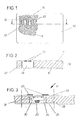
- the ID card 10 consists, as usual, of a card body 12, which is laminated on the top and bottom with a cover film 14, 16 each.
- the film can be applied in the so-called cold lamination process, i. H. without applying heat.
- the card body 12 can be made entirely of plastic, but a multi-layer body made of paper is also possible, which can additionally have all the authenticity features that are common with identity cards.
- a support member 18 is inserted, which is disc-shaped in the embodiment shown. It can have a diameter of 15-20 mm.
- the diameter of the disk-shaped carrier element is essentially determined by the number of contacts. By reducing the number of contacts, the diameter can also be reduced.
- the element is inserted into a corresponding window provided in the card body 12, the diameter of which is somewhat larger than the outside diameter of the carrier element.
- An annular gap 22 thus remains around the support element, the size of which must be such that even when the identification card is bent to a maximum, there is no direct contact of the inner walls of the window with the support element 18.
- the carrier element 18 is held in the window only by the two elastic cover films 14, 16, which are self-adhesive, so that the element 18 remains immovably positioned in the window.
- the cover film 16 has a cutout 24 in the area of the connection surfaces 20 of the carrier element 18, which enables access to the contacts 20. Both cover foils 14, 16 are preferably printed. A covering printed image 9 can be provided in particular in the area of the recess 24 in order to optically cover the connection point between the identity card and the carrier element.
- the film can also have other security or functional features, such as an additional magnetic track.
- the carrier element is described in more detail below with reference to FIG. 3; it consists of a lower cover film 26 which is coated with an adhesive and on which a thickness compensation film 18 is placed.
- the Dikken compensation film has punched-outs 34 which are large enough to be able to freely accommodate an IC module 30.
- the carrier element 18 is covered by a conductor foil 32, on the front of which there are the contact areas 20 and on the rear of which the conductor tracks 31 for the IC module 30 are located.
- the conductor tracks 31 are plated through with the contact surfaces 20 on the front.
- the contact surfaces 20 preferably have the same thickness as the thickness of the cover film 16, so that the surface of the contacts is directly aligned with the surface of the card and the contacts constantly clean themselves by friction.
- the height or thickness of the entire carrier element corresponds to the thickness of the identification card minus the thickness of the lower cover film 14.
- the IC module 30 is fixed in the interior of the carrier element 18 by an elastic adhesive mass 33, for example a drop of silicone adhesive.
- the cover film 26 and the thickness compensation film 28 are relatively stiff, so that the carrier element 18 is overall very rigid and cannot be bent.
- the box construction of the element additionally stabilizes it.
- the inside of the carrier element on the elastic sili The IC module 30, which is attached by drops, is thus optimally protected.
- the conductor foil 32 is first coated on both sides with copper. Thereupon, the contact areas 20 are etched out on the front side of the conductor foil and for the IC component on the back side of the conductor tracks 31. Contact areas and conductor tracks are finally connected to one another using the through-plating process.
- a thickness compensation film 28 which can also be designed as a self-adhesive film, is then laminated onto the conductor film 32 in a correctly positioned position.
- Corresponding cutouts 34 for the IC components must first be punched out in the thickness compensation film. The cutouts must be larger than the IC chips so that they can be stored freely.
- the cover film 26 is laminated over the recess 34 receiving the module.
- the module as shown in FIG. 3, is fixed with the aid of an elastic adhesive mass 33.
- the carrier element 18 is punched out of the film structure (dashed lines in FIG. 3), so that it can be used as an individual element in the window provided on the ID card.
- the identification card consists at this stage of production of the card inlay 12, on which the front-side cover film 16, which has the recess 24 for the contact surfaces of the carrier element, is laminated on.
- the recess 24 associated with the contact surface 20 can be used for positioning.
- the positioning can also take place by means of a corresponding shaping of the carrier element, which is adapted to the window of the card, by means of a tongue and groove catch or the like. After inserting the carrier element, the back cover film is finally laminated on.
- the positioning is carried out automatically, the carrier elements, fastened on a conveyor belt, being fed to a corresponding device together with the ID cards to be fitted in isochronous fashion.
- the positioning aid possibly provided on the carrier element and ID card for manual production can be omitted, i. H. the carrier element can also be circular.
- the two cover foils 14 and 16 are made of highly elastic material compared to the material of the carrier element 18.
- the deformation work is largely absorbed by the elastic foils.
- the support element itself remains largely unaffected by the bend.
- the carrier element is made very rigid in relation to the materials of the identity card, the deformation work must be completely absorbed in front of the cover foils. This completely eliminates damage to the carrier element. In contrast to the first-mentioned case, in which the carrier element absorbs a small part of the deformation work, it must be depleted earlier; Cover sheet material are expected.
Landscapes
- Engineering & Computer Science (AREA)
- Computer Hardware Design (AREA)
- Microelectronics & Electronic Packaging (AREA)
- Physics & Mathematics (AREA)
- General Physics & Mathematics (AREA)
- Theoretical Computer Science (AREA)
- Credit Cards Or The Like (AREA)
- Financial Or Insurance-Related Operations Such As Payment And Settlement (AREA)
- Structures Or Materials For Encapsulating Or Coating Semiconductor Devices Or Solid State Devices (AREA)
- Calculators And Similar Devices (AREA)
Abstract
Description
Die Erfindung betrifft eine Ausweiskarte mit IC-Baustein zur Verarbeitung elektrischer Signale, der mit einem separaten Trägerelement verbunden ist, das in ein Fenster des Kartenkörpers eingesetzt ist, wobei die Kontaktflächen und die mit ihnen verbundenen Leiterbahnen zum Betrieb des Bausteins auf dem Trägerelement angeordnet sind.The invention relates to an identification card with an IC module for processing electrical signals, which is connected to a separate carrier element which is inserted into a window of the card body, the contact surfaces and the interconnects connected to them for operating the module being arranged on the carrier element.
Aus der DE-A 2 659 573 ist bereits eine derartige Ausweiskarte bekannt. Der Baustein ist mit allen Zuleitungen und Kontakten auf einer Trägerplatte befestigt, die wiederum in eine Aussparung oder ein Fenster der Ausweiskarte eingesetzt ist. Die Trägerplatte ist mit der Ausweiskarte durch Verkleben bzw. Verschweißen starr verbunden. Die Kontaktflächen befinden sich auf der gleichen Seite der Trägerplatte wie der aufgeklebte IC-Baustein. Der Zugang zu den Kontakten ist daher nur über entsprechende Löcher in derAusweiskarte möglich.Such an ID card is already known from DE-A 2 659 573. The module is attached to a carrier plate with all leads and contacts, which in turn is inserted into a recess or a window in the ID card. The carrier plate is rigidly connected to the ID card by gluing or welding. The contact areas are on the same side of the carrier plate as the glued-on IC module. Access to the contacts is therefore only possible via corresponding holes in the ID card.
Die bekannte Karte zeigt erstmals einen Weg auf, wie die diffizilen IC-Bausteine in Ausweiskarten eingebettet werden können. Der bekannte Kartenaufbau weist jedoch noch so viele Nachteile auf, daß an eine praktische Verwendung dieser mit IC-Bausteinen ausgerüsteten Ausweiskarten voerst nicht zu denken ist. Eine besondere Schwierigkeit ist die Verbindung des IC-Bauteils bzw. der Trägerplatte, auf der der IC-Bauteil aufgeklebt ist mit dem Kartenmaterial. Derartige Ausweiskarten werden bekanntlich durch den täglichen Gebrauch starken Biegebelastungen ausgesetzt, die sich bei dem bekannten Aufbau direkt auf die Zuleitungen des IC-Bausteins übertragen. Durch diese Wechsel beanspruchung kann es zu Zuleitungsunterbrechungen und Defekten des IC-Bausteins kom men.The well-known card shows for the first time a way how the difficult IC components can be embedded in ID cards. However, the known card structure still has so many disadvantages that a practical use of these ID cards equipped with IC modules is initially out of the question. A particular difficulty is the connection of the IC component or the carrier plate on which the IC component is glued to the card material. Identity cards of this type are known to be exposed to strong bending loads due to daily use, which in the known structure are transferred directly to the leads of the IC module. This alternating stress can lead to lead interruptions and defects in the IC module.
Infolge der unterschiedlichen Biegesteifigkeit der Trägerplatte einerseits und der Ausweiskarte andererseits kommt es an den Verbindungsnähten zu hohen Spannungskonzentrationen, die leicht zu einem Aufreißen und damit Lösen der Trägerplatte von der Ausweiskarte führen.As a result of the different bending stiffness of the carrier plate on the one hand and the identification card on the other hand, high stress concentrations occur at the connecting seams, which easily lead to tearing and thus detachment of the carrier plate from the identification card.
Abgesehen von diesen grundsätzlichen Schwierigkeiten weist der bekannte Kartenaufbau noch weitere, durch seine spezifische Bauart bedingte Nachteile auf. Da die Kontaktflächen nur durch Löcher in der Ausweiskarte selbst zugänglich sind, besteht die Notwendigkeit, die Löcher mit leitendem Material zu füllen, um eine Verschmutzung der Kontakte zu verhindern. Dies erfordert einen zusätzlichen Arbeitsgang. Die Trägerplatte mit dem IC-Baustein hat eine solche Höhe, jedenfalls im eingebauten Zustand, daß sie nur in dem Bereich einer genormten Karte angeordnet werden kann, in dem Prägeausbuchtungen erlaubt sind. Diese Prägebereiche sind nach geltender Norm nur auf eine Zeilenbreite beschränkt, der IC-Baustein benötigt aber eine Ausbuchtung, die sich über mehrere Zeilen erstreckt Es ist daher nicht möglich, die bekannten Karten so auszubilden, daß sie der geltenden Norm entsprechen.Apart from these fundamental difficulties, the known card structure has further disadvantages due to its specific design. Since the contact areas are only accessible through holes in the ID card itself, there is a need to fill the holes with conductive material to prevent contamination of the contacts. This requires an additional operation. The carrier plate with the IC component has such a height, at least when installed, that it can only be arranged in the area of a standardized card in which embossing protrusions are permitted. According to the applicable standard, these embossing areas are limited to one line width, but the IC module requires a bulge that extends over several lines. It is therefore not possible to design the known cards in such a way that they comply with the applicable standard.
Die für die Einlagerung der Trägerplatten erforderlichen mehrstufigen Ausbuchtungen mit unterschiedlichen Materialstärken sind bezüglich ihrer Herstellung relativ aufwendig, sie lassen sich darüber hinaus nur bei Vollplastik-Ausweiskarten anbringen.The multi-stage bulges with different material thicknesses required for the storage of the carrier plates are relatively complex to manufacture, and can only be attached to full plastic ID cards.
Aus der US-A-3 702464 ist eine Ausweiskarte mit einem eingebetteten IC-Baustein bekannt, wobei der IC zum Teil mit einem elastischen Material umgeben ist. An der Unterseite des IC's erfolgt die Kontaktierung mit den Leiterbahnen, die im Kartenmaterial fest verankert, zu einer Stirnseite der Ausweiskarte geführt werden. Diese Anordnung hat eine Reihe von Nachteilen, die sich insbesondere beim täglichen Gebrauch negativ auswirken. Insbesondere wird hier lediglich der IC-Baustein in gewisser Weise durch das ihn umgebende elastische Material geschützt. Bei Verbiegungen konzentrieren sich jedoch die gesamten Kräfte auf die Kontaktstellen, da der Schaltkreis nicht vollständig mit elastischem Material umgeben ist. Ausweichbewegungen desselben sind nur möglich, soweit dies die Kontaktstellen erlauben, die jedoch üblicherweise als starre Verbindungen ausgeführt sind. Eine weitere Schwachstelle der bekannten Ausweiskarte sind die Leiterbahnen. Da diese fest verankert im Kartenmaterial große Flächen überstreichen, ist ein Bruch dieser Bahnen bei starken Druckbelastungen, denen die Karte im täglichen Gebrauch ausgesetzt ist, nahezu unvermeidbar.From US-A-3 702464 an identification card with an embedded IC module is known, the IC being partially surrounded by an elastic material. On the underside of the IC, contact is made with the conductor tracks, which are firmly anchored in the card material, to an end face of the ID card. This arrangement has a number of disadvantages, which have a negative effect, particularly in daily use. In particular, only the IC chip is protected to some extent by the elastic material surrounding it. In the event of bending, however, the entire forces concentrate on the contact points, since the circuit is not completely surrounded by elastic material. Evasive movements of the same are only possible insofar as this is permitted by the contact points, which however are usually designed as rigid connections. Another weak point of the known ID card is the conductor tracks. Since these anchored over large areas firmly anchored in the map material, breaking of these webs is almost inevitable in the event of heavy pressure loads to which the map is exposed in daily use.
Der Erfindung liegt die Aufgabe zugrunde, eine Ausweiskarte der eingangs bezeichneten Art zu schaffen, bei der die Verbindung zwischen dem Trägerelement mit dem IC-Baustein und dem Kartenkörper so gestaltet ist, daß sie auch sehr starken Biegewechselbelastungen standhält.The invention has for its object to provide an identification card of the type mentioned, in which the connection between the carrier element with the IC chip and the card body is designed so that it withstands very strong alternating bending loads.
Erfindungsgemäß wird die Aufgabe durch die im Kennzeichen des Hauptanspruchs angegebenen Merkmale gelöst.According to the invention the object is achieved by the features specified in the characterizing part of the main claim.
Bei der Erfindung wird von der Erkenntnis Gebrauch gemacht, daß nicht der IC-Baustein selbst, sondern bereits ein Zwischenerzeugnis in der Karte eingelagert werden muß, das den IC-Baustein und sämtliche zugehörigen Kontaktelemente aufweist. Die Fertigung dieses Trägerelements kann bei der dafür spezialisierten Elektronikfirma unter Verwendung hochwertiger Materialien und entsprechender Ansprüche an die Fertigung erfolgen. Das Einbringen der Trägerelemente in die Ausweiskarten dagegen kann unter Verwendung des üblichen Know-hows bei dem auf Ausweiskartenherstellung spezialisierten Erzeuger erfolgen. Voraussetzung für den Erfolg der Erfindung ist die Ausgestaltung des Trägerelements als geschlossene Einheit, in dessen Innerem der IC-Baustein gelagert ist auf dessen einer Seite sich die Kontaktflächen befinden. Beim Einsetzen des Trägerelements in ein entsprechend geformtes Fenster des Kartenkörpers bleibt rings um das Trägerelement ein Zwischenraum, so daß auch bei extremer Biegung der Ausweiskarte kein direkter körperlicher Kontakt zwischen den Innenwänden des Fensters und Trägerelement, etwa durch ein Verkeilen, erfolgen kann. Das Trägerelement wird in seiner Lage durch elastische Verbindungselemente, die den Spalt zwischen Trägerelement und Kartenkörper überbrücken, festgehalten. Die Überbrückung des Spaltes kann dabei durch Ausfüllen des Spaltes mit elastischem Material vorgenommen werden.In the invention, use is made of the knowledge that it is not the IC module itself, but rather an intermediate product that has the IC module and all associated contact elements that must already be stored in the card. This carrier element can be manufactured at the specialized electronics company using high-quality materials and corresponding demands on the manufacture. On the other hand, the carrier elements can be introduced into the identity cards using the usual know-how at the manufacturer who specializes in producing identity cards. A prerequisite for the success of the invention is the configuration of the carrier element as a closed unit, inside which the IC component is mounted, on one side of which the contact surfaces are located. When the carrier element is inserted into a correspondingly shaped window of the card body, an intermediate space remains around the carrier element space, so that even with extreme bending of the identity card no direct physical contact between the inner walls of the window and carrier element, for example by wedging, can take place. The position of the carrier element is held in place by elastic connecting elements which bridge the gap between the carrier element and the card body. The gap can be bridged by filling the gap with elastic material.
Gemäß einer vorteilhaften Weiterbildung der Erfindung werden die elastischen Verbindungselemente durch auf Ober- und/oder Unterseite des Kartenkörpers aufkaschierte Deckfolien gebildet. Das Trägerelement wird dabei lediglich von den Deckfolien, die beispielsweise selbstklebend sein können, im Fenster gehalten. Eine der Deckfolien muß selbstverständlich im Bereich der Kontaktflächen des Trägerelements eine entsprechende Aussparung aufweisen. Die Kontakte sind also, ohne einen zusätzlichen Arbeitsgang vorsehen zu müssen, frei zugänglich und somit selbstreinigend. Da die Deckfolien im sogenannten Kaltkaschierverfahren aufgebracht werden, wird der IC-Baustein auch thermisch nicht belastet.According to an advantageous development of the invention, the elastic connecting elements are formed by cover foils laminated onto the top and / or bottom of the card body. The carrier element is only held in the window by the cover foils, which can be self-adhesive, for example. One of the cover foils must of course have a corresponding recess in the area of the contact surfaces of the carrier element. The contacts are therefore freely accessible and therefore self-cleaning without having to provide an additional work step. Since the cover foils are applied using the so-called cold lamination process, the IC module is also not thermally stressed.
Weitere vorteilhafte Ausgestaltungen der Erfindung sind Gegenstand von Unteransprüchen.Further advantageous embodiments of the invention are the subject of dependent claims.
Durch die schwimmende Lagerung des als geschlossene Einheit ausgebildeten Trägerelements in einem Fenster des Kartenkörpers erhält die Karte auch unter extremen Wechselbelastungen eine solche Haltbarkeit, daß damit erstmals ihr praktischer Einsatz ermöglicht wird.The floating mounting of the carrier element, which is designed as a closed unit, in a window of the card body gives the card such a durability even under extreme alternating loads that it is possible for its practical use for the first time.
Nachfolgend ist eine Ausführungsform der Erfindung anhand der Zeichnung beispielsweise beschrieben. Darin zeigt
- Fig. 1 eine Draufsicht auf eine Ausweiskarte mit eingesetztem Trägerelement,
- Fig. einen Querschnitt durch die Ausweiskarte und das Trägerelement und
- Fig. 3 einen Querschnitt durch das Trägerelement allein.
- 1 is a plan view of an identification card with an inserted carrier element,
- Fig. A cross section through the ID card and the carrier element and
- Fig. 3 shows a cross section through the carrier element alone.
Bei dem gezeigten Ausführungsbeispiel ist das Fenster, in das das Trägerelement einsetzt ist, in einer Ecke der Ausweiskarte außerhalb der Hauptspannungsachsen angeordnet. Eine solche Anordnung hat sich als vorteilhaft erwiesen, weil sich die Karte in diesem Bereich nicht so stark verformt. Die Ausweiskarte 10 besteht wie üblich aus einem Kartenkörper 12, der auf Ober- und Unterseite mit je einer Deckfolie 14, 16 kaschiert ist. Das Aufbringen der Folie kann im sogenannten Kaltkaschierverfahren erfolgen, d. h. ohne Anwendung von Wärme. Der Kartenkörper 12 kann Vollplastik sein, möglich ist jedoch auch ein Mehrschichtenkörper aus Papier, der sämtliche, bei Ausweiskarten übliche Echtheitsmerkmale zusätzlich aufweisen kann.In the exemplary embodiment shown, the window in which the carrier element is inserted is arranged in a corner of the identification card outside the main stress axes. Such an arrangement has proven to be advantageous because the card does not deform as much in this area. The
In das kreisrunde Fenster in der oberen linken Ecke der Ausweiskarte (Fig. 1) ist ein Trägerelement 18 eingesetzt, das bei dem gezeigten Ausführungsbeispiel scheibenförmig ist. Es kann einen Durchmesser von 15-20 mm aufweisen. Der Durchmesser des scheibenförmigen Trägerelements ist im wesentlichen durch die Anzahl der Kontakte bestimmt. Mit der Reduzierung der Zahl der Kontakte kann somit auch der Durchmesser verkleinert werden.In the circular window in the upper left corner of the identity card (Fig. 1), a
Das Element ist in ein entsprechendes, im Kartenkörper 12 vorgesehenes Fenster, eingesetzt, dessen Durchmesser etwas größer als der Außendurchmesser des Trägerelements ist. Rings um das Trägerelement bleibt somit ein Ringspalt 22 stehen, dessen Größe so bemessen sein muß, daß auch bei einem maximalen Verbiegen der Ausweiskarte keine direkte Berührung der Innenwände des Fensters mit dem Trägerelement 18 erfolgt.The element is inserted into a corresponding window provided in the
Das Trägerelement 18 wird in dem Fenster lediglich durch die beiden elastischen Deckfolien 14, 16 gehalten, die selbstklebend sind, so daß das Element 18 unverrückbar in dem Fenster positioniert bleibt.The
Die Deckfolie 16 weist im Bereich der Anschlußflächen 20 des Trägerelements 18 eine Aussparung 24 auf, die einen Zugang zu den Kontakten 20 ermöglicht. Vorzugsweise sind beide Deckfolien 14, 16 bedruckt. Besonders im Bereich der Aussparung 24 kann ein deckendes Druckbild 9 vorgesehen sein, um damit die Verbindungsstelle zwischen Ausweiskarte und Trägerelement optisch abzudecken. Die Folie kann außerdem weitere Sicherheits- oder Funktionsmerkmale aufweisen, wie beispielsweise eine zusätzliche Magnetpiste.The cover film 16 has a
Nachfolgend wird unter Bezugnahme auf Fig. 3 das Trägerelement näher beschrieben, es besteht aus einer unteren Deckfolie 26, die mit einem Klebstoff beschichtet ist und auf die eine Dicken-Ausgleichsfolie 18 aufgelegt ist. Die Dikken-Ausgleichsfolie weist Ausstanzungen 34 auf, die groß genug sind, um einen IC-Baustein 30 frei aufnehmen zu können. Auf der Oberseite ist das Trägerelement 18 von einer Leiterfolie 32 abgedeckt, auf deren Vorderseite sich die Kontaktflächen 20 und auf deren Rückseite sich die Leiterbahnen 31 für den IC-Baustein 30 befinden. Die Leiterbahnen 31 sind mit den Kontaktflächen 20 auf der Vorderseite durchkontaktiert.The carrier element is described in more detail below with reference to FIG. 3; it consists of a
Die Kontaktflächen 20 haben vorzugsweise die gleiche Dicke wie die Dicke der Deckfolie 16, so daß die Oberfläche der Kontakte direkt mit der Oberfläche der Karte fluchtet und die Kontakte durch Reibung sich ständig selbst reinigen. Die Höhe bzw. Dicke des gesamten Trägerelements entspricht in diesem Fall der Dicke der Ausweiskarte abzüglich der Dicke der unteren Deckfolie 14.The contact surfaces 20 preferably have the same thickness as the thickness of the cover film 16, so that the surface of the contacts is directly aligned with the surface of the card and the contacts constantly clean themselves by friction. In this case, the height or thickness of the entire carrier element corresponds to the thickness of the identification card minus the thickness of the
Der IC-Baustein 30 wird im Inneren des Trägerelements 18 von einer elastischen Klebstoffmasse 33, beispielsweise einem Tropfen Silikonkleber, fixiert.The
Die Deckfolie 26 und die Dicken-Ausgleichsfolie 28 sind relativ steif, so daß das Trägerelement 18 insgesamt sehr starr ist und nicht verbogen werden kann. Die Kastenbauweise des Elements stabilisiert dieses noch zusätzlich. Der im Inneren des Trägerelements auf dem elastischen Silikontropfen befestigte IC-Baustein 30 ist somit optimal geschützt.The
Zur Herstellung des Trägerelements 18 wird zunächst die Leiterfolie 32 beidseitig mit Kupfer beschichtet. Daraufhin werden auf der Vorderseite der Leiterfolie die Kontaktflächen 20 und auf der Rückseite der Leiterbahnen 31 für den IC-Baustein ausgeätzt. Kontaktflächen und Leiterbahnen werden schließlich im Durchkontaktier-Verfahren miteinander verbunden.To manufacture the
Auf die Leiterfolie 32 wird anschließend eine Dicken-Ausgleichsfolie 28, die auch als Selbst klebefolie ausgebildet sein kann, in richtig positionierter Lage auflaminiert. Zuvor müssen in der Dicken-Ausgleichsfolie entsprechende Aussparungen 34 für die IC-Bausteine ausgestanzt werden. Die Aussparungen müssen größer sein als die IC-Bausteine, damit diese frei gelagert werden können.A
Nachdem der IC-Baustein 30 nach bekannten Herstellverfahren mit den Leiterbahnenden 31 verbunden worden ist, kaschiert man über die den Baustein aufnehmende Aussparung 34 die Deckfolie 26.After the
Dabei wird der Baustein, wie Fig. 3 zeigt, mit Hilfe einer elastischen Klebstoffmasse 33 fixiert.The module, as shown in FIG. 3, is fixed with the aid of an elastic
Für die manuelle Einzelfertigung von Ausweiskarten wird das Trägerelement 18 aus dem Folienverband ausgestanzt (strichlierte Linien in Fig. 3), so daß es als Einzelelement in das vorgesehene Fenster der Ausweiskarte eingesetzt werden kann. Die Ausweiskarte besteht in diesem Fertigungsstadium aus dem Karteninlett 12, auf dem die forderseitige Deckfolie 16, die die Aussparung 24 für die Kontaktflächen des Trä gerelement aufweist, auflaminiert ist.For the manual individual production of ID cards, the
Zur Positionierung kann die den Kontaktflä chen 20 zugeordnete Aussparung 24 benutzt werden. Die Positionierung kann auch durch eine entsprechende, dem Fenster der Karte angepaßte, Formgebung des Trägerelements durch eine Nut-Feder-Verrastung oder ähnliches erfolgen. Nach dem Einsetzen des Trägerelements wird schließlich die rückseitige Deckfolie auflaminiert.The
Für die Serienfertigung von IC-Ausweiskarten erfolgt die Positionierung automatisch, wobei die Trägerelemente, auf einem Transportband befestigt, gemeinsam mit den zu bestückenden Ausweiskarten taktsynchron einer entsprechenden Einrichtung zugeführt werden.For the serial production of IC ID cards, the positioning is carried out automatically, the carrier elements, fastened on a conveyor belt, being fed to a corresponding device together with the ID cards to be fitted in isochronous fashion.
In diesem Fall kann die an Trägerelement und Ausweiskarte für die manuelle Fertigung ggf. vorgesehene Positionierhilfe entfallen, d. h. das Trägerelement kann auch kreisförmig ausgebildet sein.In this case, the positioning aid possibly provided on the carrier element and ID card for manual production can be omitted, i. H. the carrier element can also be circular.
Unabhängig von der Art der Fertigung sind die beiden Deckfolien 14 und 16 aus hochelastischem Material im Vergleich zum Material des Trägerelements 18. Beim Biegen der Karte im Bereich des Fensters wird die Formänderungsarbeit zum größten Teil von den elastischen Folien aufgenommen. Das Trägerelement selbst bleibt von der Biegung weitgehend unbeeinflußt.Regardless of the type of manufacture, the two cover foils 14 and 16 are made of highly elastic material compared to the material of the
Wird das Trägerelement gegenüber den Materialien der Ausweiskarte sehr starr ausgeführt muß die Formänderungsarbeit vollständig vor den Deckfolien aufgenommen werden. Damit is eine Beschädigung des Trägerelements gänzlict ausgeschlossen. Es muß aber im Gegensatz zun erstgenannten Fall, bei dem das Trägerelemen einen geringen Teil der Formänderungsarbei aufnimmt, mit einer früheren Ermüdung de; Deckfolienmaterials gerechnet werden.If the carrier element is made very rigid in relation to the materials of the identity card, the deformation work must be completely absorbed in front of the cover foils. This completely eliminates damage to the carrier element. In contrast to the first-mentioned case, in which the carrier element absorbs a small part of the deformation work, it must be depleted earlier; Cover sheet material are expected.
Abschließend sei erwähnt, daß die optischE Gestaltung der Karte durch das eingebettet: Trägerelement kaum beeinflußt wird. Die KartE kann also sowohl für die automatische als auct für die manuelle Prüfung eingesetzt werden.Finally, please note that the optically e design of the card embedded by the: support element is hardly affected. The KartE can therefore be used both for automatic and auct for manual testing.
Claims (10)
Priority Applications (1)
| Application Number | Priority Date | Filing Date | Title |
|---|---|---|---|
| AT80102694T ATE9516T1 (en) | 1979-05-17 | 1980-05-14 | ID CARD WITH IC COMPONENT. |
Applications Claiming Priority (2)
| Application Number | Priority Date | Filing Date | Title |
|---|---|---|---|
| DE2920012A DE2920012B1 (en) | 1979-05-17 | 1979-05-17 | ID card with IC module and method for producing such an ID card |
| DE2920012 | 1979-05-17 |
Publications (2)
| Publication Number | Publication Date |
|---|---|
| EP0019280A1 EP0019280A1 (en) | 1980-11-26 |
| EP0019280B1 true EP0019280B1 (en) | 1984-09-19 |
Family
ID=6071016
Family Applications (1)
| Application Number | Title | Priority Date | Filing Date |
|---|---|---|---|
| EP80102694A Expired EP0019280B1 (en) | 1979-05-17 | 1980-05-14 | Identity card with an integrated circuit component |
Country Status (5)
| Country | Link |
|---|---|
| US (1) | US4417413A (en) |
| EP (1) | EP0019280B1 (en) |
| JP (2) | JPS5626451A (en) |
| AT (1) | ATE9516T1 (en) |
| DE (1) | DE2920012B1 (en) |
Families Citing this family (117)
| Publication number | Priority date | Publication date | Assignee | Title |
|---|---|---|---|---|
| DE3019207A1 (en) * | 1980-05-20 | 1981-11-26 | GAO Gesellschaft für Automation und Organisation mbH, 8000 München | CARRIER ELEMENT FOR AN IC CHIP |
| DE3029667A1 (en) * | 1980-08-05 | 1982-03-11 | GAO Gesellschaft für Automation und Organisation mbH, 8000 München | CARRIER ELEMENT FOR AN IC COMPONENT |
| DE3029939A1 (en) * | 1980-08-07 | 1982-03-25 | GAO Gesellschaft für Automation und Organisation mbH, 8000 München | ID CARD WITH IC COMPONENT AND METHOD FOR THEIR PRODUCTION |
| DE3131216C3 (en) * | 1981-04-14 | 1994-09-01 | Gao Ges Automation Org | ID card with IC module |
| DE3118298A1 (en) * | 1981-05-08 | 1982-12-02 | Gao Ges Automation Org | ID CARD WITH STORED IC BLOCK |
| DE3122981A1 (en) * | 1981-06-10 | 1983-01-05 | GAO Gesellschaft für Automation und Organisation mbH, 8000 München | METHOD FOR INSTALLING IC COMPONENTS IN ID CARD |
| US4501960A (en) * | 1981-06-22 | 1985-02-26 | Motorola, Inc. | Micropackage for identification card |
| DE3130324A1 (en) * | 1981-07-31 | 1983-02-17 | GAO Gesellschaft für Automation und Organisation mbH, 8000 München | CARRIER ELEMENT FOR AN IC COMPONENT |
| FR2511544A1 (en) * | 1981-08-14 | 1983-02-18 | Dassault Electronique | ELECTRONIC MODULE FOR AUTOMATIC TRANSACTION CARD AND CARD COMPRISING SUCH A MODULE |
| FR2514179A1 (en) * | 1981-10-07 | 1983-04-08 | Rockall France Sa Ste Nle | IDENTIFICATION LABEL OF OBJECTS AND APPARATUS FOR USE THEREOF |
| JPS5892597A (en) * | 1981-11-28 | 1983-06-01 | 大日本印刷株式会社 | Manufacture of identification card |
| DE3151408C1 (en) * | 1981-12-24 | 1983-06-01 | GAO Gesellschaft für Automation und Organisation mbH, 8000 München | ID card with an IC module |
| JPS58118297A (en) * | 1981-12-31 | 1983-07-14 | 共同印刷株式会社 | Manufacture of identification card |
| JPS58110473U (en) * | 1982-01-22 | 1983-07-27 | 凸版印刷株式会社 | card |
| JPS58134456A (en) * | 1982-02-04 | 1983-08-10 | Dainippon Printing Co Ltd | Ic card |
| FR2527036A1 (en) * | 1982-05-14 | 1983-11-18 | Radiotechnique Compelec | METHOD FOR CONNECTING A SEMICONDUCTOR TO ELEMENTS OF A SUPPORT, PARTICULARLY A PORTABLE CARD |
| DE3235650A1 (en) * | 1982-09-27 | 1984-03-29 | Philips Patentverwaltung Gmbh, 2000 Hamburg | INFORMATION CARD AND METHOD FOR THEIR PRODUCTION |
| JPS5983285A (en) * | 1982-11-04 | 1984-05-14 | Toppan Printing Co Ltd | Production of card |
| JPS59103163A (en) * | 1982-12-03 | 1984-06-14 | Casio Comput Co Ltd | Sheet type miniature electronic device |
| US4511796A (en) * | 1982-12-09 | 1985-04-16 | Seiichiro Aigo | Information card |
| DE3248385A1 (en) * | 1982-12-28 | 1984-06-28 | GAO Gesellschaft für Automation und Organisation mbH, 8000 München | ID CARD WITH INTEGRATED CIRCUIT |
| JPS59229686A (en) * | 1983-06-09 | 1984-12-24 | Toshiba Corp | Ic card |
| FR2548409B1 (en) * | 1983-06-29 | 1985-11-15 | Sligos | PROCESS FOR THE MANUFACTURE OF MEMORY CARDS, INSTALLATION AND MEMORY CARDS OBTAINED |
| FR2548857B1 (en) * | 1983-07-04 | 1987-11-27 | Cortaillod Cables Sa | PROCESS FOR THE CONTINUOUS MANUFACTURE OF A PRINTED CARD |
| US4663664A (en) * | 1983-10-31 | 1987-05-05 | R. F. Monolithics, Inc. | Electronic ticket method and apparatus for television signal scrambling and descrambling |
| US4539472A (en) * | 1984-01-06 | 1985-09-03 | Horizon Technology, Inc. | Data processing card system and method of forming same |
| DE3420051A1 (en) * | 1984-05-29 | 1985-12-05 | GAO Gesellschaft für Automation und Organisation mbH, 8000 München | DATA CARRIER WITH IC COMPONENT AND METHOD FOR PRODUCING SUCH A DATA CARRIER |
| US4677528A (en) * | 1984-05-31 | 1987-06-30 | Motorola, Inc. | Flexible printed circuit board having integrated circuit die or the like affixed thereto |
| JPS61131185A (en) * | 1984-11-30 | 1986-06-18 | Casio Comput Co Ltd | Ic card |
| DE3435506A1 (en) * | 1984-09-27 | 1986-04-03 | Siemens AG, 1000 Berlin und 8000 München | Arrangement with an information store, attached to an object for marking purposes |
| JPS61123990A (en) * | 1984-11-05 | 1986-06-11 | Casio Comput Co Ltd | Ic card |
| US4661653A (en) * | 1984-12-27 | 1987-04-28 | Seiichiro Aigo | Package assembly for semiconductor device |
| JPS61157990A (en) * | 1984-12-29 | 1986-07-17 | Kyodo Printing Co Ltd | Ic card |
| JPH0751390B2 (en) * | 1985-07-10 | 1995-06-05 | カシオ計算機株式会社 | IC card |
| US4889980A (en) * | 1985-07-10 | 1989-12-26 | Casio Computer Co., Ltd. | Electronic memory card and method of manufacturing same |
| US5203078A (en) * | 1985-07-17 | 1993-04-20 | Ibiden Co., Ltd. | Printed wiring board for IC cards |
| US4727668A (en) * | 1985-09-03 | 1988-03-01 | Allied Corporation | Coded surveillance marker with improved biasing |
| IT1214634B (en) * | 1985-10-23 | 1990-01-18 | Pentasystem Srl | SUPPORT FOR PAPER OR CARD IN GLOBAL PLASTIC MATERIAL A MEMORY INTEGRATED CIRCUIT. |
| DE3624852A1 (en) * | 1986-01-10 | 1987-07-16 | Orga Druck Gmbh | Electronic data and/or programme carriers and production method therefor |
| JPS62214998A (en) * | 1986-03-17 | 1987-09-21 | 三菱電機株式会社 | Thin-type semiconductor card |
| JPH0696356B2 (en) * | 1986-03-17 | 1994-11-30 | 三菱電機株式会社 | Thin semiconductor card |
| JPS62218196A (en) * | 1986-03-20 | 1987-09-25 | 日立マクセル株式会社 | Integrated circuit card |
| US4766293A (en) * | 1986-06-26 | 1988-08-23 | Visa International Service Association | Portable financial transaction card capable of authorizing a transaction in foreign currencies |
| JPH0524554Y2 (en) * | 1986-07-21 | 1993-06-22 | ||
| US5478995A (en) * | 1986-10-23 | 1995-12-26 | Skidata Computer Gesellschaft M.B.H. | Data carrier with disc shaped carrier structure |
| US5202550A (en) * | 1986-10-23 | 1993-04-13 | Skidata Computer Gesellschaft M.B.H. | Device for machine communication in data transmission |
| DE3639630A1 (en) * | 1986-11-20 | 1988-06-01 | Gao Ges Automation Org | DATA CARRIER WITH INTEGRATED CIRCUIT AND METHOD FOR PRODUCING THE SAME |
| JPS62276660A (en) * | 1987-03-31 | 1987-12-01 | Casio Comput Co Ltd | Production of compact electronic equipment |
| US4980679A (en) * | 1987-07-17 | 1990-12-25 | Klaubert Earl C | Time varying identification badge |
| JPH0753988Y2 (en) * | 1987-09-14 | 1995-12-13 | 凸版印刷株式会社 | IC card |
| JPH01108095A (en) * | 1987-10-20 | 1989-04-25 | Ryoden Kasei Co Ltd | Ic card |
| FR2624999B1 (en) * | 1987-12-22 | 1990-04-06 | Sgs Thomson Microelectronics | METHOD FOR MANUFACTURING CHIP CARDS |
| FR2627879B1 (en) * | 1988-02-26 | 1990-06-15 | Sgs Thomson Microelectronics | INSERTING PROCESS FOR CHIP CARDS |
| US4921160A (en) * | 1988-02-29 | 1990-05-01 | American Telephone And Telegraph Company | Personal data card and method of constructing the same |
| GB8901189D0 (en) * | 1989-01-19 | 1989-03-15 | Avery W & T Limited | Portable electronic token |
| USRE35578E (en) * | 1988-12-12 | 1997-08-12 | Sgs-Thomson Microelectronics, Inc. | Method to install an electronic component and its electrical connections on a support, and product obtained thereby |
| DE3924439A1 (en) * | 1989-07-24 | 1991-04-18 | Edgar Schneider | CARRIER ELEMENT WITH AT LEAST ONE INTEGRATED CIRCUIT, ESPECIALLY FOR INSTALLATION IN CHIP CARDS, AND METHOD FOR THE PRODUCTION OF THESE CARRIER ELEMENTS |
| EP0440158B1 (en) * | 1990-01-30 | 1997-09-10 | Kabushiki Kaisha Toshiba | Mutual authentication system |
| JP2687661B2 (en) * | 1990-03-26 | 1997-12-08 | 三菱電機株式会社 | IC card manufacturing method |
| DE9100665U1 (en) * | 1991-01-21 | 1992-07-16 | Telbus Gesellschaft Fuer Elektronische Kommunikations-Systeme Mbh, 8057 Eching, De | |
| US5272596A (en) * | 1991-06-24 | 1993-12-21 | At&T Bell Laboratories | Personal data card fabricated from a polymer thick-film circuit |
| DE4132720A1 (en) * | 1991-10-01 | 1993-04-08 | Gao Ges Automation Org | CHIP CARD AND METHOD FOR THE PRODUCTION THEREOF |
| FR2685797B1 (en) * | 1991-12-27 | 1997-07-04 | Sagem | DOUBLE CHIP CARD. |
| JPH07164787A (en) * | 1992-03-26 | 1995-06-27 | Dainippon Printing Co Ltd | Manufacture of ic card |
| US5544014A (en) * | 1992-08-12 | 1996-08-06 | Oki Electric Industry Co., Ltd. | IC card having a built-in semiconductor integrated circuit device |
| DE4325458A1 (en) * | 1993-07-29 | 1995-02-09 | Orga Bond Technik Gmbh | Support element for an IC module |
| US5581065A (en) | 1993-08-02 | 1996-12-03 | Dai Nippon Printing Co., Ltd. | Sheet-framed IC carrier, method for producing the same, and IC carrier case |
| DE9422424U1 (en) * | 1994-02-04 | 2002-02-21 | Giesecke & Devrient Gmbh | Chip card with an electronic module |
| US5480842A (en) * | 1994-04-11 | 1996-01-02 | At&T Corp. | Method for fabricating thin, strong, and flexible die for smart cards |
| US5451763A (en) * | 1994-07-05 | 1995-09-19 | Alto Corporation | Personal medical IC card and read/write unit |
| US5599052A (en) * | 1994-12-16 | 1997-02-04 | Van Davelaar; Peter C. | Bag carrier with means for promotional indicia and/or customer identification |
| US5671271A (en) * | 1995-05-25 | 1997-09-23 | Henderson; Daniel A. | Dialer programming system and device with integrated printing process |
| US5817207A (en) | 1995-10-17 | 1998-10-06 | Leighton; Keith R. | Radio frequency identification card and hot lamination process for the manufacture of radio frequency identification cards |
| DE69626747T2 (en) | 1995-11-16 | 2003-09-04 | Matsushita Electric Ind Co Ltd | Printed circuit board and its arrangement |
| JPH09156267A (en) * | 1995-12-06 | 1997-06-17 | Watada Insatsu Kk | Plastic card |
| KR100209259B1 (en) * | 1996-04-25 | 1999-07-15 | 이해규 | Ic card and method for manufacture of the same |
| US5786988A (en) * | 1996-07-02 | 1998-07-28 | Sandisk Corporation | Integrated circuit chips made bendable by forming indentations in their back surfaces flexible packages thereof and methods of manufacture |
| FR2760113B1 (en) * | 1997-02-24 | 1999-06-04 | Gemplus Card Int | METHOD FOR MANUFACTURING A CONTACTLESS CARD WITH A COILED ANTENNA |
| FR2772529B1 (en) * | 1997-12-17 | 2000-02-04 | Smurfit Worldwide Research Eur | SUBSRAT PROVIDED WITH AN ELECTRONIC DEVICE |
| DE19811578A1 (en) * | 1998-03-17 | 1999-10-14 | Siemens Ag | Multiple layer circuit board especially for chip card |
| US6404643B1 (en) | 1998-10-15 | 2002-06-11 | Amerasia International Technology, Inc. | Article having an embedded electronic device, and method of making same |
| US6179210B1 (en) * | 1999-02-09 | 2001-01-30 | Motorola, Inc. | Punch out pattern for hot melt tape used in smartcards |
| US6421013B1 (en) | 1999-10-04 | 2002-07-16 | Amerasia International Technology, Inc. | Tamper-resistant wireless article including an antenna |
| JP4239352B2 (en) * | 2000-03-28 | 2009-03-18 | 株式会社日立製作所 | Manufacturing method of electronic device |
| US6648232B1 (en) * | 2000-10-24 | 2003-11-18 | Moore North America, Inc. | High temperature tag having enclosed transceiver |
| TWI249712B (en) * | 2001-02-28 | 2006-02-21 | Hitachi Ltd | Memory card and its manufacturing method |
| WO2003046828A1 (en) * | 2001-11-29 | 2003-06-05 | Interlock Ag | Transponder label |
| US6851617B2 (en) | 2002-04-19 | 2005-02-08 | Avery Dennison Corporation | Laser imageable RFID label/tag |
| DE10232568A1 (en) | 2002-07-18 | 2004-01-29 | Agfa-Gevaert Ag | identity card |
| US7823777B2 (en) | 2003-01-03 | 2010-11-02 | American Express Travel Related Services Company, Inc. | Metal-containing transaction card and method of making same |
| WO2004063977A2 (en) * | 2003-01-03 | 2004-07-29 | American Express Travel Related Services Company, Inc. | Metal containing transaction card and method of making the same |
| US8033457B2 (en) | 2003-01-03 | 2011-10-11 | American Express Travel Related Services Company, Inc. | Metal-containing transaction card and method of making the same |
| US20080297341A1 (en) * | 2006-09-11 | 2008-12-04 | Mcclanahan James B | Real-time passenger identification, passenger onboard inventory, location and safety monitoring system |
| JP2008246104A (en) * | 2007-03-30 | 2008-10-16 | Angel Shoji Kk | Game card incorporating rfid and its manufacturing method |
| IL184260A0 (en) * | 2007-06-27 | 2008-03-20 | On Track Innovations Ltd | Mobile telecommunications device having sim/antenna coil interface |
| TW200905753A (en) * | 2007-07-18 | 2009-02-01 | Yuen Foong Yu Paper Mfg Co Ltd | Flexible and super-thin smart card and packaging method thereof |
| US20100139138A1 (en) * | 2007-08-03 | 2010-06-10 | Cardware, Llc. | Multi-purpose auxiliary member for use with personal cards |
| US8028923B2 (en) * | 2007-11-14 | 2011-10-04 | Smartrac Ip B.V. | Electronic inlay structure and method of manufacture thereof |
| US20090123743A1 (en) * | 2007-11-14 | 2009-05-14 | Guy Shafran | Method of manufacture of wire imbedded inlay |
| US20100090008A1 (en) * | 2008-10-13 | 2010-04-15 | Oded Bashan | Authentication seal |
| US8579201B2 (en) * | 2010-01-12 | 2013-11-12 | Sustainable Cards, Llc | Hybrid card |
| US8195236B2 (en) | 2010-06-16 | 2012-06-05 | On Track Innovations Ltd. | Retrofit contactless smart SIM functionality in mobile communicators |
| DE102010025774A1 (en) * | 2010-07-01 | 2012-01-05 | Giesecke & Devrient Gmbh | Method of making an inlay for a portable data carrier and inlay |
| US8424757B2 (en) | 2010-12-06 | 2013-04-23 | On Track Innovations Ltd. | Contactless smart SIM functionality retrofit for mobile communication device |
| USD707682S1 (en) * | 2012-12-05 | 2014-06-24 | Logomotion, S.R.O. | Memory card |
| USD729808S1 (en) | 2013-03-13 | 2015-05-19 | Nagrastar Llc | Smart card interface |
| USD759022S1 (en) | 2013-03-13 | 2016-06-14 | Nagrastar Llc | Smart card interface |
| US9888283B2 (en) | 2013-03-13 | 2018-02-06 | Nagrastar Llc | Systems and methods for performing transport I/O |
| USD758372S1 (en) | 2013-03-13 | 2016-06-07 | Nagrastar Llc | Smart card interface |
| US9647997B2 (en) | 2013-03-13 | 2017-05-09 | Nagrastar, Llc | USB interface for performing transport I/O |
| JP6143510B2 (en) * | 2013-03-21 | 2017-06-07 | 株式会社東芝 | IC card manufacturing method |
| USD780763S1 (en) | 2015-03-20 | 2017-03-07 | Nagrastar Llc | Smart card interface |
| USD864968S1 (en) | 2015-04-30 | 2019-10-29 | Echostar Technologies L.L.C. | Smart card interface |
| JP1647727S (en) * | 2018-02-01 | 2019-12-09 | ||
| WO2019173455A1 (en) * | 2018-03-07 | 2019-09-12 | X-Card Holdings, Llc | Metal card |
| USD930000S1 (en) | 2018-10-12 | 2021-09-07 | Huawei Technologies Co., Ltd. | Memory card |
| CN110278886A (en) * | 2019-07-22 | 2019-09-27 | 杭州沃朴物联科技有限公司 | A kind of anti-drop structure and the anti-dropout managing device equipped with the structure |
Family Cites Families (10)
| Publication number | Priority date | Publication date | Assignee | Title |
|---|---|---|---|---|
| US2637994A (en) * | 1950-01-28 | 1953-05-12 | Harrison Jr | Key holder |
| US3637994A (en) * | 1970-10-19 | 1972-01-25 | Trw Inc | Active electrical card device |
| US3702464A (en) * | 1971-05-04 | 1972-11-07 | Ibm | Information card |
| US3934122A (en) * | 1974-08-15 | 1976-01-20 | Riccitelli James A | Electronic security card and system for authenticating card ownership |
| US4004133A (en) * | 1974-12-30 | 1977-01-18 | Rca Corporation | Credit card containing electronic circuit |
| FR2337381A1 (en) * | 1975-12-31 | 1977-07-29 | Honeywell Bull Soc Ind | PORTABLE CARD FOR ELECTRICAL SIGNAL PROCESSING SYSTEM AND PROCESS FOR MANUFACTURING THIS CARD |
| US4222516A (en) * | 1975-12-31 | 1980-09-16 | Compagnie Internationale Pour L'informatique Cii-Honeywell Bull | Standardized information card |
| US4105156A (en) * | 1976-09-06 | 1978-08-08 | Dethloff Juergen | Identification system safeguarded against misuse |
| FR2439438A1 (en) * | 1978-10-19 | 1980-05-16 | Cii Honeywell Bull | RIBBON CARRYING ELECTRIC SIGNAL PROCESSING DEVICES, MANUFACTURING METHOD THEREOF AND APPLICATION THEREOF TO A SIGNAL PROCESSING ELEMENT |
| US4200227A (en) * | 1978-12-26 | 1980-04-29 | Lemelson Jerome H | Key assembly for electronic system |
-
1979
- 1979-05-17 DE DE2920012A patent/DE2920012B1/en active Granted
-
1980
- 1980-05-14 EP EP80102694A patent/EP0019280B1/en not_active Expired
- 1980-05-14 AT AT80102694T patent/ATE9516T1/en not_active IP Right Cessation
- 1980-05-16 JP JP6414880A patent/JPS5626451A/en active Granted
-
1982
- 1982-11-29 US US06/444,964 patent/US4417413A/en not_active Expired - Lifetime
-
1991
- 1991-08-23 JP JP3212138A patent/JPH054483A/en active Granted
Also Published As
| Publication number | Publication date |
|---|---|
| JPH0561116B2 (en) | 1993-09-03 |
| JPH054483A (en) | 1993-01-14 |
| JPH0380638B2 (en) | 1991-12-25 |
| JPS5626451A (en) | 1981-03-14 |
| EP0019280A1 (en) | 1980-11-26 |
| DE2920012B1 (en) | 1980-11-20 |
| ATE9516T1 (en) | 1984-10-15 |
| DE2920012C2 (en) | 1988-09-29 |
| US4417413A (en) | 1983-11-29 |
Similar Documents
| Publication | Publication Date | Title |
|---|---|---|
| EP0019280B1 (en) | Identity card with an integrated circuit component | |
| DE102005058101B4 (en) | Chip card and method for producing a chip card | |
| DE3019207C2 (en) | ||
| EP0268830B1 (en) | Data carrier with integrated circuit and process for making the same | |
| DE19645083C2 (en) | Contactless chip card with transponder coil | |
| EP0140230B1 (en) | Integrated circuit record carrier and process for making the same | |
| EP0689164B1 (en) | Method for producing recording medium | |
| DE3131216C3 (en) | ID card with IC module | |
| EP0919041B1 (en) | Process for manufacturing a chip card module for a combined chip card | |
| DE4243654C2 (en) | Thin IC card | |
| EP1271399B1 (en) | Data carrier with integrated circuit | |
| DE60116540T2 (en) | Security label for storing information | |
| DE3741925C2 (en) | ||
| EP0902973B1 (en) | Substrate for a semiconductor chip | |
| WO1995022121A1 (en) | Combined chip card | |
| WO1996018974A1 (en) | Foil design for mounting smart cards with coils | |
| DE3723547A1 (en) | CARRIER ELEMENT FOR INSTALLATION IN ID CARD | |
| WO2001015074A1 (en) | Method for producing a chip card and chip card produced according to said method | |
| CH663115A5 (en) | CARRIER ELEMENT WITH A SEMICONDUCTOR PLATE HAVING AN INTEGRATED CIRCUIT FOR INSTALLATION IN A DATA CARRIER, ESPECIALLY IN AN ID CARD. | |
| EP0757330A2 (en) | Method of producing a data carrier | |
| EP0996932A1 (en) | Data carrier which can be operated without contact | |
| DE19703057A1 (en) | Carrier element for semiconductor chip esp. for combination chip card | |
| EP0521502A1 (en) | Procedure for setting-in a carrier member | |
| DE3111516A1 (en) | Identity card with IC chip | |
| DE102010046965A1 (en) | Transponder inlay for a personal identification document and a method of making a transponder inlay |
Legal Events
| Date | Code | Title | Description |
|---|---|---|---|
| PUAI | Public reference made under article 153(3) epc to a published international application that has entered the european phase |
Free format text: ORIGINAL CODE: 0009012 |
|
| AK | Designated contracting states |
Designated state(s): AT BE CH FR GB IT LU NL SE |
|
| ITCL | It: translation for ep claims filed |
Representative=s name: STUDIO ING. ALFREDO RAIMONDI |
|
| 17P | Request for examination filed |
Effective date: 19810522 |
|
| ITF | It: translation for a ep patent filed |
Owner name: STUDIO ING. ALFREDO RAIMONDI |
|
| GRAA | (expected) grant |
Free format text: ORIGINAL CODE: 0009210 |
|
| AK | Designated contracting states |
Designated state(s): AT BE CH FR GB IT LI LU NL SE |
|
| REF | Corresponds to: |
Ref document number: 9516 Country of ref document: AT Date of ref document: 19841015 Kind code of ref document: T |
|
| ET | Fr: translation filed | ||
| PLBE | No opposition filed within time limit |
Free format text: ORIGINAL CODE: 0009261 |
|
| STAA | Information on the status of an ep patent application or granted ep patent |
Free format text: STATUS: NO OPPOSITION FILED WITHIN TIME LIMIT |
|
| 26N | No opposition filed | ||
| ITTA | It: last paid annual fee | ||
| REG | Reference to a national code |
Ref country code: GB Ref legal event code: 746 Effective date: 19940512 |
|
| EPTA | Lu: last paid annual fee | ||
| ITPR | It: changes in ownership of a european patent |
Owner name: OFFERTA DI LICENZA AL PUBBLICO |
|
| EAL | Se: european patent in force in sweden |
Ref document number: 80102694.9 |
|
| REG | Reference to a national code |
Ref country code: FR Ref legal event code: D6 |
|
| PGFP | Annual fee paid to national office [announced via postgrant information from national office to epo] |
Ref country code: SE Payment date: 19980427 Year of fee payment: 19 |
|
| PGFP | Annual fee paid to national office [announced via postgrant information from national office to epo] |
Ref country code: GB Payment date: 19980429 Year of fee payment: 19 |
|
| PGFP | Annual fee paid to national office [announced via postgrant information from national office to epo] |
Ref country code: FR Payment date: 19980518 Year of fee payment: 19 |
|
| PGFP | Annual fee paid to national office [announced via postgrant information from national office to epo] |
Ref country code: AT Payment date: 19980522 Year of fee payment: 19 |
|
| PGFP | Annual fee paid to national office [announced via postgrant information from national office to epo] |
Ref country code: CH Payment date: 19980528 Year of fee payment: 19 |
|
| PGFP | Annual fee paid to national office [announced via postgrant information from national office to epo] |
Ref country code: NL Payment date: 19980531 Year of fee payment: 19 |
|
| PGFP | Annual fee paid to national office [announced via postgrant information from national office to epo] |
Ref country code: LU Payment date: 19980604 Year of fee payment: 19 |
|
| PGFP | Annual fee paid to national office [announced via postgrant information from national office to epo] |
Ref country code: BE Payment date: 19980806 Year of fee payment: 19 |
|
| PG25 | Lapsed in a contracting state [announced via postgrant information from national office to epo] |
Ref country code: LU Free format text: LAPSE BECAUSE OF NON-PAYMENT OF DUE FEES Effective date: 19990514 Ref country code: GB Free format text: LAPSE BECAUSE OF NON-PAYMENT OF DUE FEES Effective date: 19990514 Ref country code: AT Free format text: LAPSE BECAUSE OF NON-PAYMENT OF DUE FEES Effective date: 19990514 |
|
| PG25 | Lapsed in a contracting state [announced via postgrant information from national office to epo] |
Ref country code: SE Free format text: LAPSE BECAUSE OF NON-PAYMENT OF DUE FEES Effective date: 19990515 |
|
| PG25 | Lapsed in a contracting state [announced via postgrant information from national office to epo] |
Ref country code: LI Free format text: LAPSE BECAUSE OF NON-PAYMENT OF DUE FEES Effective date: 19990531 Ref country code: CH Free format text: LAPSE BECAUSE OF NON-PAYMENT OF DUE FEES Effective date: 19990531 Ref country code: BE Free format text: LAPSE BECAUSE OF NON-PAYMENT OF DUE FEES Effective date: 19990531 |
|
| BERE | Be: lapsed |
Owner name: GAO-G. FUR AUTOMATION UND ORGANISATION M.B.H. Effective date: 19990531 |
|
| PG25 | Lapsed in a contracting state [announced via postgrant information from national office to epo] |
Ref country code: NL Free format text: LAPSE BECAUSE OF NON-PAYMENT OF DUE FEES Effective date: 19991201 |
|
| REG | Reference to a national code |
Ref country code: CH Ref legal event code: PL |
|
| GBPC | Gb: european patent ceased through non-payment of renewal fee |
Effective date: 19990514 |
|
| EUG | Se: european patent has lapsed |
Ref document number: 80102694.9 |
|
| PG25 | Lapsed in a contracting state [announced via postgrant information from national office to epo] |
Ref country code: FR Free format text: LAPSE BECAUSE OF NON-PAYMENT OF DUE FEES Effective date: 20000131 |
|
| NLV4 | Nl: lapsed or anulled due to non-payment of the annual fee |
Effective date: 19991201 |
|
| REG | Reference to a national code |
Ref country code: FR Ref legal event code: ST |